CN106960651B - Display device and driving method thereof - Google Patents
Display device and driving method thereofDownload PDFInfo
- Publication number
- CN106960651B CN106960651BCN201611030771.0ACN201611030771ACN106960651BCN 106960651 BCN106960651 BCN 106960651BCN 201611030771 ACN201611030771 ACN 201611030771ACN 106960651 BCN106960651 BCN 106960651B
- Authority
- CN
- China
- Prior art keywords
- data driver
- voltage
- display panel
- amplifier
- display
- Prior art date
- Legal status (The legal status is an assumption and is not a legal conclusion. Google has not performed a legal analysis and makes no representation as to the accuracy of the status listed.)
- Active
Links
Images


Classifications
- G—PHYSICS
- G09—EDUCATION; CRYPTOGRAPHY; DISPLAY; ADVERTISING; SEALS
- G09G—ARRANGEMENTS OR CIRCUITS FOR CONTROL OF INDICATING DEVICES USING STATIC MEANS TO PRESENT VARIABLE INFORMATION
- G09G3/00—Control arrangements or circuits, of interest only in connection with visual indicators other than cathode-ray tubes
- G09G3/20—Control arrangements or circuits, of interest only in connection with visual indicators other than cathode-ray tubes for presentation of an assembly of a number of characters, e.g. a page, by composing the assembly by combination of individual elements arranged in a matrix no fixed position being assigned to or needed to be assigned to the individual characters or partial characters
- G—PHYSICS
- G06—COMPUTING OR CALCULATING; COUNTING
- G06F—ELECTRIC DIGITAL DATA PROCESSING
- G06F1/00—Details not covered by groups G06F3/00 - G06F13/00 and G06F21/00
- G06F1/26—Power supply means, e.g. regulation thereof
- G06F1/32—Means for saving power
- G06F1/3203—Power management, i.e. event-based initiation of a power-saving mode
- G06F1/3234—Power saving characterised by the action undertaken
- G06F1/3296—Power saving characterised by the action undertaken by lowering the supply or operating voltage
- G—PHYSICS
- G09—EDUCATION; CRYPTOGRAPHY; DISPLAY; ADVERTISING; SEALS
- G09G—ARRANGEMENTS OR CIRCUITS FOR CONTROL OF INDICATING DEVICES USING STATIC MEANS TO PRESENT VARIABLE INFORMATION
- G09G3/00—Control arrangements or circuits, of interest only in connection with visual indicators other than cathode-ray tubes
- G09G3/20—Control arrangements or circuits, of interest only in connection with visual indicators other than cathode-ray tubes for presentation of an assembly of a number of characters, e.g. a page, by composing the assembly by combination of individual elements arranged in a matrix no fixed position being assigned to or needed to be assigned to the individual characters or partial characters
- G09G3/34—Control arrangements or circuits, of interest only in connection with visual indicators other than cathode-ray tubes for presentation of an assembly of a number of characters, e.g. a page, by composing the assembly by combination of individual elements arranged in a matrix no fixed position being assigned to or needed to be assigned to the individual characters or partial characters by control of light from an independent source
- G09G3/3406—Control of illumination source
- G09G3/342—Control of illumination source using several illumination sources separately controlled corresponding to different display panel areas, e.g. along one dimension such as lines
- G—PHYSICS
- G09—EDUCATION; CRYPTOGRAPHY; DISPLAY; ADVERTISING; SEALS
- G09G—ARRANGEMENTS OR CIRCUITS FOR CONTROL OF INDICATING DEVICES USING STATIC MEANS TO PRESENT VARIABLE INFORMATION
- G09G3/00—Control arrangements or circuits, of interest only in connection with visual indicators other than cathode-ray tubes
- G09G3/20—Control arrangements or circuits, of interest only in connection with visual indicators other than cathode-ray tubes for presentation of an assembly of a number of characters, e.g. a page, by composing the assembly by combination of individual elements arranged in a matrix no fixed position being assigned to or needed to be assigned to the individual characters or partial characters
- G09G3/22—Control arrangements or circuits, of interest only in connection with visual indicators other than cathode-ray tubes for presentation of an assembly of a number of characters, e.g. a page, by composing the assembly by combination of individual elements arranged in a matrix no fixed position being assigned to or needed to be assigned to the individual characters or partial characters using controlled light sources
- G09G3/30—Control arrangements or circuits, of interest only in connection with visual indicators other than cathode-ray tubes for presentation of an assembly of a number of characters, e.g. a page, by composing the assembly by combination of individual elements arranged in a matrix no fixed position being assigned to or needed to be assigned to the individual characters or partial characters using controlled light sources using electroluminescent panels
- G09G3/32—Control arrangements or circuits, of interest only in connection with visual indicators other than cathode-ray tubes for presentation of an assembly of a number of characters, e.g. a page, by composing the assembly by combination of individual elements arranged in a matrix no fixed position being assigned to or needed to be assigned to the individual characters or partial characters using controlled light sources using electroluminescent panels semiconductive, e.g. using light-emitting diodes [LED]
- G09G3/3208—Control arrangements or circuits, of interest only in connection with visual indicators other than cathode-ray tubes for presentation of an assembly of a number of characters, e.g. a page, by composing the assembly by combination of individual elements arranged in a matrix no fixed position being assigned to or needed to be assigned to the individual characters or partial characters using controlled light sources using electroluminescent panels semiconductive, e.g. using light-emitting diodes [LED] organic, e.g. using organic light-emitting diodes [OLED]
- G09G3/3275—Details of drivers for data electrodes
- G09G3/3291—Details of drivers for data electrodes in which the data driver supplies a variable data voltage for setting the current through, or the voltage across, the light-emitting elements
- G—PHYSICS
- G09—EDUCATION; CRYPTOGRAPHY; DISPLAY; ADVERTISING; SEALS
- G09G—ARRANGEMENTS OR CIRCUITS FOR CONTROL OF INDICATING DEVICES USING STATIC MEANS TO PRESENT VARIABLE INFORMATION
- G09G3/00—Control arrangements or circuits, of interest only in connection with visual indicators other than cathode-ray tubes
- G09G3/20—Control arrangements or circuits, of interest only in connection with visual indicators other than cathode-ray tubes for presentation of an assembly of a number of characters, e.g. a page, by composing the assembly by combination of individual elements arranged in a matrix no fixed position being assigned to or needed to be assigned to the individual characters or partial characters
- G09G3/34—Control arrangements or circuits, of interest only in connection with visual indicators other than cathode-ray tubes for presentation of an assembly of a number of characters, e.g. a page, by composing the assembly by combination of individual elements arranged in a matrix no fixed position being assigned to or needed to be assigned to the individual characters or partial characters by control of light from an independent source
- G09G3/36—Control arrangements or circuits, of interest only in connection with visual indicators other than cathode-ray tubes for presentation of an assembly of a number of characters, e.g. a page, by composing the assembly by combination of individual elements arranged in a matrix no fixed position being assigned to or needed to be assigned to the individual characters or partial characters by control of light from an independent source using liquid crystals
- G09G3/3611—Control of matrices with row and column drivers
- G09G3/3685—Details of drivers for data electrodes
- G—PHYSICS
- G09—EDUCATION; CRYPTOGRAPHY; DISPLAY; ADVERTISING; SEALS
- G09G—ARRANGEMENTS OR CIRCUITS FOR CONTROL OF INDICATING DEVICES USING STATIC MEANS TO PRESENT VARIABLE INFORMATION
- G09G3/00—Control arrangements or circuits, of interest only in connection with visual indicators other than cathode-ray tubes
- G09G3/20—Control arrangements or circuits, of interest only in connection with visual indicators other than cathode-ray tubes for presentation of an assembly of a number of characters, e.g. a page, by composing the assembly by combination of individual elements arranged in a matrix no fixed position being assigned to or needed to be assigned to the individual characters or partial characters
- G09G3/34—Control arrangements or circuits, of interest only in connection with visual indicators other than cathode-ray tubes for presentation of an assembly of a number of characters, e.g. a page, by composing the assembly by combination of individual elements arranged in a matrix no fixed position being assigned to or needed to be assigned to the individual characters or partial characters by control of light from an independent source
- G09G3/36—Control arrangements or circuits, of interest only in connection with visual indicators other than cathode-ray tubes for presentation of an assembly of a number of characters, e.g. a page, by composing the assembly by combination of individual elements arranged in a matrix no fixed position being assigned to or needed to be assigned to the individual characters or partial characters by control of light from an independent source using liquid crystals
- G09G3/3611—Control of matrices with row and column drivers
- G09G3/3696—Generation of voltages supplied to electrode drivers
- G—PHYSICS
- G09—EDUCATION; CRYPTOGRAPHY; DISPLAY; ADVERTISING; SEALS
- G09G—ARRANGEMENTS OR CIRCUITS FOR CONTROL OF INDICATING DEVICES USING STATIC MEANS TO PRESENT VARIABLE INFORMATION
- G09G2310/00—Command of the display device
- G09G2310/02—Addressing, scanning or driving the display screen or processing steps related thereto
- G09G2310/0264—Details of driving circuits
- G09G2310/027—Details of drivers for data electrodes, the drivers handling digital grey scale data, e.g. use of D/A converters
- G—PHYSICS
- G09—EDUCATION; CRYPTOGRAPHY; DISPLAY; ADVERTISING; SEALS
- G09G—ARRANGEMENTS OR CIRCUITS FOR CONTROL OF INDICATING DEVICES USING STATIC MEANS TO PRESENT VARIABLE INFORMATION
- G09G2310/00—Command of the display device
- G09G2310/08—Details of timing specific for flat panels, other than clock recovery
- G—PHYSICS
- G09—EDUCATION; CRYPTOGRAPHY; DISPLAY; ADVERTISING; SEALS
- G09G—ARRANGEMENTS OR CIRCUITS FOR CONTROL OF INDICATING DEVICES USING STATIC MEANS TO PRESENT VARIABLE INFORMATION
- G09G2330/00—Aspects of power supply; Aspects of display protection and defect management
- G09G2330/02—Details of power systems and of start or stop of display operation
- G09G2330/021—Power management, e.g. power saving
- G09G2330/023—Power management, e.g. power saving using energy recovery or conservation
- G—PHYSICS
- G09—EDUCATION; CRYPTOGRAPHY; DISPLAY; ADVERTISING; SEALS
- G09G—ARRANGEMENTS OR CIRCUITS FOR CONTROL OF INDICATING DEVICES USING STATIC MEANS TO PRESENT VARIABLE INFORMATION
- G09G2340/00—Aspects of display data processing
- G09G2340/04—Changes in size, position or resolution of an image
- G09G2340/0407—Resolution change, inclusive of the use of different resolutions for different screen areas
- G09G2340/0435—Change or adaptation of the frame rate of the video stream
Landscapes
- Engineering & Computer Science (AREA)
- Theoretical Computer Science (AREA)
- Physics & Mathematics (AREA)
- General Physics & Mathematics (AREA)
- Computer Hardware Design (AREA)
- Chemical & Material Sciences (AREA)
- Crystallography & Structural Chemistry (AREA)
- General Engineering & Computer Science (AREA)
- Control Of Indicators Other Than Cathode Ray Tubes (AREA)
- Liquid Crystal Display Device Control (AREA)
Abstract
Description
Translated fromChinese本申请要求享有于2015年11月24日提交的韩国专利申请第10-2015-0164911号的优先权,在此为了所有目的通过引用将该申请并入本申请,如同在此被完全阐述一样。This application claims priority to Korean Patent Application No. 10-2015-0164911 filed on November 24, 2015, which is hereby incorporated by reference for all purposes as if fully set forth herein.
技术领域technical field
本公开内容涉及一种显示装置及其驱动方法。The present disclosure relates to a display device and a driving method thereof.
背景技术Background technique
随着信息技术的发展,在使用者与信息之间起媒介作用的显示器的市场正在增长。因此,诸如有机发光显示器(OLED)、量子点显示器(QDD)、液晶显示器(LCD)和等离子体显示面板(PDP)之类的显示装置正越来越多地被使用。With the development of information technology, the market for displays that mediate between users and information is growing. Therefore, display devices such as Organic Light Emitting Displays (OLEDs), Quantum Dot Displays (QDDs), Liquid Crystal Displays (LCDs) and Plasma Display Panels (PDPs) are increasingly being used.
上述显示装置均包括:包含多个子像素的显示面板、输出驱动信号以驱动显示面板的驱动部、产生并向驱动部提供电力的电源。The above-mentioned display devices all include: a display panel including a plurality of sub-pixels, a driving unit that outputs a driving signal to drive the display panel, and a power source that generates and supplies power to the driving unit.
显示装置可形成为小尺寸、中尺寸或大尺寸。对于小型显示器来说,即使是以毫瓦计的功耗也对确定电池寿命起重要作用。由于该原因,已常规地提出延长小型或中型显示器的操作时间(运行时间)的各种方法。The display device may be formed in a small size, a medium size, or a large size. For small displays, even power consumption in milliwatts plays an important role in determining battery life. For this reason, various methods of extending the operation time (operation time) of small or medium-sized displays have been conventionally proposed.
常规地,为了延长小型或中型显示器的操作(运行)时间,在显示面板上不显示图像的显示关闭时段期间,应暂时关闭显示面板,或者应降低亮度。此外,在此时段期间应降低显示面板的驱动频率。然而,常规提出的方法仍需改进,因此应继续对其进行研究。Conventionally, in order to prolong the operation (operation) time of a small or medium-sized display, during a display off period in which no image is displayed on the display panel, the display panel should be temporarily turned off, or the brightness should be lowered. In addition, the driving frequency of the display panel should be reduced during this period. However, the conventionally proposed methods still need to be improved, so research on them should be continued.
发明内容SUMMARY OF THE INVENTION
本公开内容提供了一种显示装置,包括显示面板、数据驱动器和节能部。所述显示面板显示图像。所述数据驱动器向所述显示面板提供数据信号。所述节能部根据所述显示面板的显示模式控制用于所述数据驱动器的基准源。The present disclosure provides a display device including a display panel, a data driver, and a power saving part. The display panel displays images. The data driver provides data signals to the display panel. The power saving section controls a reference source for the data driver according to a display mode of the display panel.
在另一方面中,本公开内容提供了一种显示装置的驱动方法。所述显示装置的驱动方法包括:分析输入图像并确定显示面板的显示模式是否是节能模式;如果显示面板的显示模式是节能模式,则选择按帧调光或按水平线调光;以及根据所选择的调光方法控制用于数据驱动器的基准源。In another aspect, the present disclosure provides a driving method of a display device. The driving method of the display device includes: analyzing an input image and determining whether a display mode of the display panel is an energy-saving mode; if the display mode of the display panel is an energy-saving mode, selecting frame-wise dimming or horizontal-line dimming; and according to the selected The dimming method controls the reference source for the data driver.
附图说明Description of drawings
被包括用来给本发明提供进一步理解并结合在本说明书中组成本说明书一部分的附图图解了本发明的实施方式,并与说明书一起用于解释本发明的原理。在附图中:The accompanying drawings, which are included to provide a further understanding of the invention and are incorporated in and constitute a part of this specification, illustrate embodiments of the invention and together with the description serve to explain the principles of the invention. In the attached image:
图1是示意地示出根据本公开内容示例性实施方式的显示装置的框图;FIG. 1 is a block diagram schematically illustrating a display device according to an exemplary embodiment of the present disclosure;
图2是示意地示出图1的子像素的构造的示图;FIG. 2 is a diagram schematically showing the configuration of the sub-pixel of FIG. 1;
图3是示意地示出根据本公开内容示例性实施方式的智能手表的框图;3 is a block diagram schematically illustrating a smart watch according to an exemplary embodiment of the present disclosure;
图4是示意地示出智能手表的显示面板的俯视平面图;4 is a top plan view schematically showing a display panel of a smart watch;
图5是示出显示面板根据节能方法的变化的示图;FIG. 5 is a diagram illustrating a change of a display panel according to a power saving method;
图6是解释根据测试例的节能方法的电压波形图;6 is a voltage waveform diagram explaining a power saving method according to a test example;
图7是解释根据本公开内容示例性实施方式的节能方法的电压波形图;7 is a voltage waveform diagram explaining a power saving method according to an exemplary embodiment of the present disclosure;
图8是示出根据本公开内容示例性实施方式的节能方法的应用例的图;FIG. 8 is a diagram illustrating an application example of a power saving method according to an exemplary embodiment of the present disclosure;
图9是解释根据本公开内容示例性实施方式的节能方法的流程图;FIG. 9 is a flowchart explaining a power saving method according to an exemplary embodiment of the present disclosure;
图10和11是解释根据本公开内容示例性实施方式的显示装置的实质部分的框图;10 and 11 are block diagrams explaining essential parts of a display device according to an exemplary embodiment of the present disclosure;
图12示出了根据本公开内容示例性实施方式的显示装置的一些部分的实施例。FIG. 12 shows an example of some parts of a display device according to an exemplary embodiment of the present disclosure.
具体实施方式Detailed ways
现在将详细参考附图中所示的实施方式,附图中图解了这些实施方式的一些例子。Reference will now be made in detail to the embodiments shown in the accompanying drawings, examples of which are illustrated in the accompanying drawings.
下面将参照附图描述本公开内容的具体实施方式。Specific embodiments of the present disclosure will be described below with reference to the accompanying drawings.
图1是示意地示出根据本公开内容示例性实施方式的显示装置的框图。图2是示意地示出图1的子像素的构造的示图。FIG. 1 is a block diagram schematically illustrating a display device according to an exemplary embodiment of the present disclosure. FIG. 2 is a diagram schematically showing the configuration of the sub-pixel of FIG. 1 .
如图1中所示,显示装置主要包括主机系统1000、时序控制器170、数据驱动器130、电源140、栅极驱动器150和显示面板110。As shown in FIG. 1 , the display device mainly includes a
主机系统1000包括内置有缩放器的系统芯片(system-on-chip,SoC),主机系统1000将输入图像的数字视频数据转换成适于在显示面板110上显示的格式的数据信号。主机系统1000将各种时序信号连同数据信号一起输送到时序控制器170。The
时序控制器170基于从主机系统1000接收的诸如垂直同步信号、水平同步信号、数据使能信号和主时钟之类的时序信号控制数据驱动器130和栅极驱动器150的操作时序。时序控制器170执行对从主机系统1000接收的数据信号的图像处理(诸如数据补偿等)并将其提供到数据驱动器130。The
数据驱动器130响应于从时序控制器170输出的第一驱动信号DDC等进行操作。数据驱动器130将从时序控制器170接收的数字数据信号DATA转换成模拟数据信号并输出该模拟数据信号。数据驱动器130响应于设置在内部或外部的伽马部的伽马电压GMA将数字数据信号DATA转换成模拟数据信号。数据驱动器130将数据信号提供到显示面板110的数据线DL1至DLn。The
栅极驱动器150响应于从时序控制器170输出的第二驱动信号GDC等进行操作。栅极驱动器150以栅极高电压或栅极低电压输出栅极信号(或扫描信号)。栅极驱动器150可沿向前或向后的方向按顺序输出栅极信号。栅极驱动器150将栅极信号提供到显示面板110的栅极线GL1至GLm。The
电源140产生用于驱动数据驱动器130等的第一电压源VCC和GND、以及用于驱动显示面板110的第二电压源EVDD和EVSS。此外,电源140产生驱动显示装置所需的电压,诸如被输送到栅极驱动器150的栅极高电压、栅极低电压等。The
显示面板110包括子像素SP、连接到子像素SP的数据线DL1至DLn、以及连接到子像素SP的栅极线GL1至GLm。显示面板110响应于从栅极驱动器150输出的栅极信号和从数据驱动器130输出的数据信号DATA显示图像。显示面板110包括下基板和上基板,子像素SP形成在下基板与上基板之间。The
如图2中所示,一个子像素包括连接到栅极线GL1和数据线DL1(或形成在栅极线GL1与数据线DL1的交叉部分处)的开关薄膜晶体管SW、以及响应于通过开关薄膜晶体管SW提供的数据信号DATA而操作的像素电路PC。As shown in FIG. 2, one sub-pixel includes a switching thin film transistor SW connected to the gate line GL1 and the data line DL1 (or formed at the intersection of the gate line GL1 and the data line DL1), and a switching thin film SW in response to passing through the gate line GL1 and the data line DL1. The pixel circuit PC operates in response to the data signal DATA supplied by the transistor SW.
根据子像素SP的像素电路PC的构造,显示面板110由液晶显示面板或有机发光显示面板实现。若显示面板110由液晶显示面板实现,则显示面板110以TN(扭曲向列)模式、VA(垂直取向)模式、IPS(共面切换)模式、FFS(边缘场切换)模式、或ECB(电控双折射)模式进行操作。若显示面板110由有机发光显示面板实现,则显示面板110作为顶部发光型、底部发光型或双侧发光型进行操作。According to the configuration of the pixel circuit PC of the sub-pixel SP, the
上述显示装置可实施用于电视系统、机顶盒、导航系统、视频播放器、蓝光播放器、个人电脑(PC)、可穿戴装置、家庭影院系统、移动电话等。The above-described display device may be implemented for television systems, set-top boxes, navigation systems, video players, Blu-ray players, personal computers (PCs), wearable devices, home theater systems, mobile phones, and the like.
显示装置的显示面板可以是液晶显示面板、有机发光显示面板、电泳显示面板、量子点显示面板、等离子体显示面板等。为了便于描述,作为显示面板的示例,以下将描述具有有机发光显示面板的显示装置。The display panel of the display device may be a liquid crystal display panel, an organic light emitting display panel, an electrophoretic display panel, a quantum dot display panel, a plasma display panel, or the like. For convenience of description, as an example of a display panel, a display device having an organic light emitting display panel will be described below.
以下将描述的显示装置可形成为小尺寸、中尺寸或大尺寸。当显示装置实现为要求低功耗的小型或中型显示器时,其可表现更优良的性能。The display device to be described below may be formed in a small size, a medium size, or a large size. When the display device is implemented as a small or medium-sized display requiring low power consumption, it can exhibit better performance.
作为示例,将描述根据本公开内容示例性实施方式的智能手表,智能手表属于一种小型显示器。在以下将要描述的智能手表的情形中,在显示面板上不显示图像的显示关闭时段期间可暂时关闭显示面板或降低亮度,也可在此时段期间降低显示面板的驱动频率,但将省略对它的描述。此外,将在以下描述中给出其中一个像素由红色子像素R、绿色子像素G和蓝色子像素B组成的示例。然而,应注意这只是举例说明,本公开内容并不限于此。As an example, a smart watch according to an exemplary embodiment of the present disclosure, which is a small display, will be described. In the case of a smart watch to be described below, the display panel may be temporarily turned off or the brightness may be lowered during a display-off period in which no image is displayed on the display panel, and the drive frequency of the display panel may also be lowered during this period, but it will be omitted. description of. Furthermore, an example in which one pixel is composed of a red sub-pixel R, a green sub-pixel G, and a blue sub-pixel B will be given in the following description. However, it should be noted that this is for illustration only, and the present disclosure is not limited thereto.
图3是示意地示出根据本公开内容示例性实施方式的智能手表的框图。图4是示意地示出智能手表的显示面板的俯视平面图。FIG. 3 is a block diagram schematically illustrating a smart watch according to an exemplary embodiment of the present disclosure. FIG. 4 is a top plan view schematically showing a display panel of the smart watch.
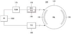
如图3中所示,智能手表100包括主机系统(HS)1000、时序控制器(TCON)170、数据驱动器(DIC)130、电源(PIC)140、栅极驱动器150、显示面板(PNL)110和触摸驱动器190。As shown in FIG. 3 , the
智能手表100对应于小型显示器。在小型显示器中,装置的一些部分被集成,以减小装置的复杂性。例如,电源140可包括在数据驱动器130中。然而,这只是举例说明,小型显示器可以以各种构造实现,包括将时序控制器170和数据驱动器130集成到单个单元中。The
栅极驱动器150与像素阵列一起内嵌于显示面板110中。内嵌于显示面板110中的栅极驱动器150与薄膜晶体管工艺一起通过GIP(面板内栅极)技术形成。The
智能手表100具有触摸驱动器190,触摸驱动器190作为触摸型输入手段帮助使用者输入数据。此外,显示面板110包括触摸传感器和传感器线,触摸传感器使用触摸驱动器190感测触摸位置并输出感测位置的值,传感器线将触摸传感器和触摸驱动器190电连接。The
触摸驱动器190使用自电容触摸传感器或互电容触摸传感器检测关于手指触摸位置的信息。触摸驱动器190将检测的关于手指触摸位置的信息输送到主机系统1000。主机系统1000执行与从触摸驱动器190接收的触摸位置信息相关的应用程序。The
如图4中所示,显示面板例如可形成为圆形。除圆形之外,显示面板110还可形成为包括正方形、矩形、多边形、椭圆形等在内的各种形状。As shown in FIG. 4 , the display panel may be formed in a circular shape, for example. In addition to a circle, the
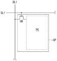
红色子像素R、绿色子像素G和蓝色子像素B以及触摸传感器(未图示)置于显示面板110的显示区域AA中。焊盘部111a可置于显示面板110的非显示区域(或边框区)BZ中界定的焊盘区域PA中。作为示例,焊盘部111a仅置于显示区域AA的顶部上,但也可以置于显示区域AA的下方。The red sub-pixel R, the green sub-pixel G, and the blue sub-pixel B and a touch sensor (not shown) are placed in the display area AA of the
数据驱动器130(代替数据驱动器,其可实现为集成电路)安装在柔性电路基板180上。柔性电路基板180通过各向异性导电膜(ACF)等电连接到焊盘部111a。The data driver 130 (in place of the data driver, which may be implemented as an integrated circuit) is mounted on the
如上所述,对于小型显示器来说,即使是以毫瓦计的功耗也对确定电池寿命起重要作用。由于该原因,已常规地提出延长小型或中型显示器的操作时间(运行时间)的各种方法。As mentioned above, for small displays, even power consumption in milliwatts plays an important role in determining battery life. For this reason, various methods of extending the operation time (operation time) of small or medium-sized displays have been conventionally proposed.
常规地,为了延长小型或中型显示器的操作时间(运行时间),在显示面板上不显示图像的显示关闭时段期间,应暂时关闭显示面板,或者应降低亮度。此外,在此时段期间应降低显示面板的驱动频率。然而,常规提出的方法仍需改进,因此应继续对其进行研究。Conventionally, in order to prolong the operation time (operation time) of a small or medium-sized display, during a display off period in which no image is displayed on the display panel, the display panel should be temporarily turned off, or the brightness should be lowered. In addition, the driving frequency of the display panel should be reduced during this period. However, the conventionally proposed methods still need to be improved, so research on them should be continued.
以下,将考虑根据测试例的节能方法,并且将描述改进此方法的示例性实施方式。Hereinafter, an energy saving method according to a test example will be considered, and an exemplary embodiment to improve this method will be described.
图5是示出显示面板根据节能方法的变化的示图。图6是解释根据测试例的节能方法的电压波形图。FIG. 5 is a diagram illustrating a change of a display panel according to a power saving method. FIG. 6 is a voltage waveform diagram explaining a power saving method according to a test example.
如图5中所示,为了延长小型或中型显示器的操作时间(运行时间),在显示面板上不显示图像的显示关闭时段期间,应暂时关闭显示面板,或者应降低亮度。As shown in FIG. 5, in order to prolong the operation time (operation time) of the small or medium-sized display, the display panel should be temporarily turned off or the brightness should be lowered during the display off period in which no image is displayed on the display panel.
与在显示面板上显示图像的显示开启时段对应的图5的部分(a)和(d)可定义为正常模式,因为显示面板以正常方式操作。相比之下,与在显示面板上不显示图像的显示关闭时段对应的图5的部分(b)和(c)可定义为节能模式,因为显示面板以减小功耗的方式操作。Parts (a) and (d) of FIG. 5 corresponding to the display-on period in which an image is displayed on the display panel may be defined as a normal mode because the display panel operates in a normal manner. In contrast, parts (b) and (c) of FIG. 5 corresponding to the display-off period in which no image is displayed on the display panel can be defined as the power saving mode because the display panel operates in a manner that reduces power consumption.
如图6所示,在根据测试例的节能方法中,当显示面板的显示模式从正常模式NOR变为节能模式PSM时,被提供到伽马转换器Gamma DAC的伽马转换器电压GMAV发生变化。As shown in FIG. 6 , in the power saving method according to the test example, when the display mode of the display panel is changed from the normal mode NOR to the power saving mode PSM, the gamma converter voltage GMAV supplied to the gamma converter Gamma DAC changes .
例如,当显示模式是正常模式NOR时,最大电压Max被提供到数据驱动器的伽马转换器Gamma DAC。相比之下,当显示模式是节能模式PSM时,最小电压Min被提供到数据驱动器的伽马转换器Gamma DAC。改变提供到伽马转换器Gamma DAC的伽马转换器电压GMAV会改变亮度。For example, when the display mode is the normal mode NOR, the maximum voltage Max is supplied to the gamma converter Gamma DAC of the data driver. In contrast, when the display mode is the power saving mode PSM, the minimum voltage Min is supplied to the gamma converter Gamma DAC of the data driver. Changing the gamma converter voltage GMAV supplied to the gamma converter Gamma DAC changes the brightness.
如此,为了改变提供到数据驱动器的伽马转换器Gamma DAC的电压,可调节电源的输出电压,或者可调节数据驱动器的内部电压。As such, in order to change the voltage supplied to the gamma converter Gamma DAC of the data driver, the output voltage of the power supply may be adjusted, or the internal voltage of the data driver may be adjusted.
内部电压是指,为了使用电压驱动数据驱动器中包括的装置,数据驱动器基于从电源输出的电压而自己产生的电压。就是说,由于每个装置以不同的电压操作,因此基于从电源输出的电压产生其他电压。The internal voltage refers to a voltage that the data driver generates by itself based on the voltage output from the power supply in order to drive the devices included in the data driver using the voltage. That is, since each device operates at a different voltage, other voltages are generated based on the voltage output from the power supply.
同时,关于功耗的测试结果显示出,在根据测试例的方法中,即使在开启节能模式PSM的情况下,由于数据驱动器中消耗的静态电流成分和动态电流成分,电流消耗也没有降低(减少),甚至是在基本水平之上。Meanwhile, the test results regarding power consumption show that, in the method according to the test example, even when the power saving mode PSM is turned on, the current consumption is not reduced due to the static current component and dynamic current component consumed in the data driver (reduced ), even above the base level.
数据驱动器中的静态电流是指即使当数据驱动器通过其输出通道不产生输出时仍被默认提供到放大器的电源电压所消耗的电流。数据驱动器的动态电流是指当数据驱动器通过其输出通道输出与特定图像对应的数据信号时提供到输出端处的放大器的电源电压所消耗的电流。Quiescent current in the data driver refers to the current drawn by the supply voltage that is supplied by default to the amplifier even when the data driver is producing no output through its output channel. The dynamic current of the data driver refers to the current consumed by the power supply voltage supplied to the amplifier at the output when the data driver outputs a data signal corresponding to a specific image through its output channel.
此原因的调查揭示出,在根据测试例的方法中,不管显示模式的变化如何,数据驱动器的输出端处的放大器电压AMPV被固定为单一电压值。Investigation of this reason revealed that, in the method according to the test example, the amplifier voltage AMPV at the output terminal of the data driver was fixed to a single voltage value regardless of the change in the display mode.
基于以上测试结果,本公开内容提出如下能够进一步降低功耗的方法。Based on the above test results, the present disclosure proposes the following methods that can further reduce power consumption.
图7是解释根据本公开内容示例性实施方式的节能方法的电压波形图。图8是示出根据本公开内容示例性实施方式的节能方法的应用例的示图。图9是解释根据本公开内容示例性实施方式的节能方法的流程图。FIG. 7 is a voltage waveform diagram explaining a power saving method according to an exemplary embodiment of the present disclosure. FIG. 8 is a diagram illustrating an application example of the energy saving method according to an exemplary embodiment of the present disclosure. FIG. 9 is a flowchart explaining a power saving method according to an exemplary embodiment of the present disclosure.
如图7中所示,在根据本公开内容示例性实施方式的节能方法中,当显示面板的显示模式从正常模式NOR变为节能模式PSM时,提供到数据驱动器的伽马转换器Gamma DAC的伽马转换器电压GMAV发生变化。图7描绘了当显示模式是节能模式PSM时按帧为基础的电流消耗减少的示例。As shown in FIG. 7 , in the power saving method according to the exemplary embodiment of the present disclosure, when the display mode of the display panel is changed from the normal mode NOR to the power saving mode PSM, the gamma converter of the gamma converter Gamma DAC provided to the data driver The gamma converter voltage GMAV changes. FIG. 7 depicts an example of frame-based current consumption reduction when the display mode is the power saving mode PSM.
作为示例,当显示模式是正常模式NOR时,最大电压Max被提供到数据驱动器的伽马转换器Gamma DAC。相比之下,当显示模式是节能模式PSM时,最小电压Min被提供到数据驱动器的伽马转换器Gamma DAC。改变提供到伽马转换器Gamma DAC的伽马转换器电压GMAV会改变亮度。As an example, when the display mode is the normal mode NOR, the maximum voltage Max is supplied to the gamma converter Gamma DAC of the data driver. In contrast, when the display mode is the power saving mode PSM, the minimum voltage Min is supplied to the gamma converter Gamma DAC of the data driver. Changing the gamma converter voltage GMAV supplied to the gamma converter Gamma DAC changes the brightness.
此外,当显示面板的显示模式从正常模式NOR变为节能模式PSM时,提供到数据驱动器的放大器AMP的放大器电压AMPV发生变化。In addition, when the display mode of the display panel is changed from the normal mode NOR to the power saving mode PSM, the amplifier voltage AMPV supplied to the amplifier AMP of the data driver changes.
作为示例,当显示模式是正常模式NOR时,最大电压Max被提供到数据驱动器中的放大器。相比之下,当显示模式是节能模式PSM时,目标电压TV被提供到数据驱动器中的放大器。目标电压TV是基于初级测试(preliminary test)获得的值,其可对应于最小电压或与最小电压相当的电压。As an example, when the display mode is the normal mode NOR, the maximum voltage Max is supplied to the amplifier in the data driver. In contrast, when the display mode is the power saving mode PSM, the target voltage TV is supplied to the amplifier in the data driver. The target voltage TV is a value obtained based on a preliminary test, which may correspond to a minimum voltage or a voltage equivalent to the minimum voltage.
改变提供到数据驱动器中的放大器AMP的放大器电压AMPV的方法可根据是否显示图像而如下变化。以下将描述的图8描绘了当驱动能够以节能模式PSM驱动的、诸如时钟显示区域之类的区域时电压变化的示例。图8的圆形部分表示显示区域。The method of changing the amplifier voltage AMPV supplied to the amplifier AMP in the data driver may vary as follows according to whether or not to display an image. FIG. 8 , which will be described below, depicts an example of voltage changes when driving a region such as a clock display region that can be driven in the power saving mode PSM. The circular portion of FIG. 8 represents the display area.
如图8的(a)中所示,当数据驱动器驱动时钟显示区域DSP时,数据驱动器的输出保持为开启状态,但放大器电压AMPV以特定变化率从最大电压减小到目标电压或降低到0V。相反,如果数据驱动器移动出时钟显示区域DSP而到达非时间显示区域NDSP,则数据驱动器的输出关闭,放大器电压AMPV降到0V。就是说,没有电压被提供到数据驱动器中的放大器。As shown in (a) of FIG. 8 , when the data driver drives the clock display area DSP, the output of the data driver remains in the ON state, but the amplifier voltage AMPV decreases from the maximum voltage to the target voltage or to 0V at a specific rate of change . Conversely, if the data driver moves out of the clock display area DSP to the non-time display area NDSP, the output of the data driver is turned off and the amplifier voltage AMPV drops to 0V. That is, no voltage is supplied to the amplifier in the data driver.
如图8的(b)中所示,当数据驱动器驱动时钟显示区域DSP时,数据驱动器的输出保持为开启状态,但放大器电压AMPV从0V或目标电压上升到最大电压。相反,如果数据驱动器移动出时钟显示区域DSP而到达非时间显示区域NDSP,则数据驱动器的输出关闭,放大器电压AMPV降到0V。就是说,没有电压被提供到数据驱动器中的放大器。As shown in (b) of FIG. 8 , when the data driver drives the clock display area DSP, the output of the data driver remains in the ON state, but the amplifier voltage AMPV rises from 0V or the target voltage to the maximum voltage. Conversely, if the data driver moves out of the clock display area DSP to the non-time display area NDSP, the output of the data driver is turned off and the amplifier voltage AMPV drops to 0V. That is, no voltage is supplied to the amplifier in the data driver.
图8的(a)描绘了对于运行节能模式的区域来说,放大器电压AMPV以渐弱的方式变化的示例,图8的(b)描绘对于运行节能模式的区域来说,放大器电压AMPV以渐强的方式变化的实例。如图8中所示,按水平线调光的构思涉及按垂直时间为单位控制数据驱动器的输出通道。(a) of FIG. 8 depicts an example in which the amplifier voltage AMPV changes in a gradually decreasing manner for the region operating the power saving mode, and (b) of FIG. 8 depicts that the amplifier voltage AMPV is gradually changing for the region operating the power saving mode An example of a strong way of changing. As shown in FIG. 8, the concept of dimming by horizontal line involves controlling the output channel of the data driver in units of vertical time.
根据以上示例,数据驱动器在1帧时段期间仅改变其中运行节能模式的数据线(对应于显示区域)上的放大器电压AMPV。此外,数据驱动器将其中不产生输出的数据线(对应于非显示区域)上的放大器电压AMPV降到0V或目标电压。According to the above example, the data driver changes only the amplifier voltage AMPV on the data line (corresponding to the display area) in which the power saving mode operates during the 1 frame period. In addition, the data driver drops the amplifier voltage AMPV on the data line (corresponding to the non-display area) in which no output is generated to 0V or the target voltage.
如在本公开内容的示例性实施方式中,改变提供到放大器AMP的电压以及提供到数据驱动器的伽马转换器Gamma DAC的电压的结果表明,静态电流被降低为零或接近零,并且消耗了和显示区域所需的动态电流一样多的动态电流。As in the exemplary embodiment of the present disclosure, the result of varying the voltage supplied to the amplifier AMP and the voltage supplied to the gamma converter Gamma DAC of the data driver shows that the quiescent current is reduced to zero or close to zero, and consumes As much dynamic current as is required for the display area.
为了以本公开内容示例性实施方式中进行驱动的方式驱动显示装置,需要根据以下图9的顺序驱动装置。In order to drive the display device in the manner of driving in the exemplary embodiment of the present disclosure, it is necessary to drive the device according to the sequence of FIG. 9 below.
根据本公开内容示例性实施方式的驱动方法包括:分析输入图像并确定显示面板的显示模式是否是节能模式;如果显示面板的显示模式是节能模式,则选择按帧调光或按水平线调光;以及根据所选择的调光方法控制用于数据驱动器的基准源(referencesource)(或基准电力)。The driving method according to an exemplary embodiment of the present disclosure includes: analyzing an input image and determining whether a display mode of a display panel is an energy-saving mode; if the display mode of the display panel is an energy-saving mode, selecting frame-wise dimming or horizontal-line dimming; And the reference source (or reference power) for the data driver is controlled according to the selected dimming method.
首先,分析输入图像(S110)。通过分析输入图像数据信号的格式,可根据特定图像执行节能模式。例如,可按照使用者同意的情况执行节能模式。First, the input image is analyzed (S110). By analyzing the format of the input image data signal, the power saving mode can be executed according to a specific image. For example, the power saving mode may be executed in accordance with the user's consent.
显示面板可在以下情况进入节能模式PSM:(1)重复静止图像,(2)在特定区域(或特定线)中没有图像继续存在,(3)显示面板上显示使用者同意的图像,或(4)显示面板上显示屏保图像,但本公开内容并不限于此。The display panel may enter power saving mode PSM when: (1) a still image is repeated, (2) no image continues in a specific area (or a specific line), (3) an image with user consent is displayed on the display panel, or ( 4) A preserved image is displayed on the display panel, but the present disclosure is not limited thereto.
尽管在进入节能模式PSM之前进行图像分析并不是必须的,但作为示例,以下将基于图像分析进行描述。Although it is not necessary to perform image analysis before entering the power saving mode PSM, as an example, the following description will be based on image analysis.
接着,确定显示模式是否是节能模式PSM(S120)。如果显示模式不是节能模式(“否”),则进行图像分析直到显示面板进入节能模式PSM。Next, it is determined whether the display mode is the power saving mode PSM (S120). If the display mode is not the power saving mode ("No"), image analysis is performed until the display panel enters the power saving mode PSM.
接着,如果显示面板是节能模式(“是”),则选择按帧调光或按水平线调光(S130)。在一示例中,在按帧调光方法中,放大器电压可进行变化,以使放大器在第N帧具有第一放大器电压,在第(N+1)帧具有第二放大器电压,并在第(N+2)帧具有第三放大器电压。在此情形中,放大器电压的电平可按以下顺序变化:第一放大器电压->第二放大器电压->第三放大器电压,或者按相反的顺序变化。Next, if the display panel is in the power saving mode ("Yes"), dimming by frame or dimming by horizontal line is selected (S130). In one example, in the frame-by-frame dimming method, the amplifier voltage may be varied such that the amplifier has the first amplifier voltage at the Nth frame, the second amplifier voltage at the (N+1)th frame, and the (N+1)th frame at the amplifier voltage. The N+2) frame has a third amplifier voltage. In this case, the levels of the amplifier voltages may vary in the following order: first amplifier voltage -> second amplifier voltage -> third amplifier voltage, or in the reverse order.
在另一示例中,在按水平线调光方法中,放大器电压可进行变化,以使对于位于第一扫描线上的数据线而言放大器具有第一放大器电压,对于位于第(N+1)扫描线上的数据线而言放大器具有第二放大器电压,并且对于位于第(N+2)扫描线上的数据线而言放大器具有第三放大器电压。在此情形中,放大器电压的电平可按以下顺序变化:第一放大器电压->第二放大器电压->第三放大器电压,或者按相反的顺序变化。In another example, in the horizontal line dimming method, the amplifier voltage may be varied such that the amplifier has the first amplifier voltage for the data line located on the first scan line, and the amplifier has the first amplifier voltage for the data line located on the (N+1)th scan line. The amplifier has a second amplifier voltage for the data line on the line, and the amplifier has a third amplifier voltage for the data line on the (N+2)th scan line. In this case, the levels of the amplifier voltages may vary in the following order: first amplifier voltage -> second amplifier voltage -> third amplifier voltage, or in the reverse order.
以此方式分析输入图像提供了根据图像的特点(例如,能分割图像的显示区域)选择性地执行节能模式PSM的优点。Analyzing the input image in this way provides the advantage of selectively executing the power saving mode PSM according to the characteristics of the image (eg, the display area capable of segmenting the image).
接着,根据选择的调光方法控制放大器中的电流(S140)。可以以根据节能模式PSM的配置而控制静态电流和动态电流之一或静态电流和动态电流二者的方式控制放大器中的电流。Next, the current in the amplifier is controlled according to the selected dimming method (S140). The current in the amplifier may be controlled in such a way that one or both of the quiescent current and the dynamic current are controlled according to the configuration of the power saving mode PSM.
接着,确定显示面板是否进入正常模式NOR或者确定节能模式是否处于结束阶段(S150)。如果显示面板没有进入正常模式NOR(“否”),则可重复S130中选择按帧调光或按水平线调光的步骤及后续步骤。Next, it is determined whether the display panel enters the normal mode NOR or whether the power saving mode is in the end stage (S150). If the display panel does not enter the normal mode NOR (“No”), the step of selecting dimming by frame or dimming by horizontal line in S130 and subsequent steps may be repeated.
接着,如果显示面板进入正常模式NOR(“是”),则使放大器中的电流控制失效(S160)。一旦放大器中的电流控制失效,放大器电压就返回到最大电压并且显示模式转换到正常模式NOR,因此显示装置达到其正常操作状态。Next, if the display panel enters the normal mode NOR ("Yes"), the current control in the amplifier is disabled (S160). Once the current control in the amplifier fails, the amplifier voltage returns to the maximum voltage and the display mode transitions to the normal mode NOR, thus the display device reaches its normal operating state.
下面,将描述用于实现根据本公开内容示例性实施方式的显示装置的实质部分和基于这些实质部分的实施例。Hereinafter, essential parts for realizing the display device according to the exemplary embodiment of the present disclosure and examples based on the essential parts will be described.
图10和11是解释根据本公开内容示例性实施方式的显示装置的实质部分的框图。图12示出了根据本公开内容示例性实施方式的显示装置的一些部分的实施例。10 and 11 are block diagrams explaining essential parts of a display device according to an exemplary embodiment of the present disclosure. FIG. 12 shows an example of some parts of a display device according to an exemplary embodiment of the present disclosure.
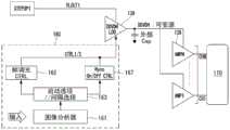
如图10中所示,根据本公开内容示例性实施方式的显示装置包括节能部160,节能部160用于控制提供到数据驱动器130中的放大器AMP的放大器电压AMPV。As shown in FIG. 10 , the display device according to the exemplary embodiment of the present disclosure includes the
节能部160包括图像分析器161、调光方法选择器(启用选项(Enable Option)/间隔选择(Interval Selection))163、帧调光控制器(帧调光CTRL)165和水平调光控制器(Hsync ON/Off CTRL)167。The
图像分析器161分析输入图像数据信号的格式。图像分析器161确定输入图像数据信号是适于节能模式还是正常模式。图像分析器161确定输入图像数据信号是对应于内置的图案还是使用者同意的图案。The
调光方法选择器(启用选项/间隔选择)163用于当显示模式被转换为节能模式时选择适于图像的调光方法。调光方法选择器163决定哪个调光方法更适于输入图像的特点,并根据所决定的调光方法运行帧调光控制器165或水平调光控制器167。The dimming method selector (enable option/interval selection) 163 is used to select a dimming method suitable for the image when the display mode is switched to the power saving mode. The
帧调光控制器(帧调光CTRL)165产生第一控制信号CTRL1,第一控制信号CTRL1用于控制数据驱动器中的放大器以启动按帧调光。在一示例中,在按帧调光方法中,放大器电压可发生变化,以使放大器在第N帧具有第一放大器电压,在第(N+1)帧具有第二放大器电压,并在第(N+2)帧具有第三放大器电压。在此情形中,放大器电压的电平可按以下顺序变化:第一放大器电压->第二放大器电压->第三放大器电压,或者按相反的顺序变化。The frame dimming controller (frame dimming CTRL) 165 generates a first control signal CTRL1, which is used to control the amplifier in the data driver to enable frame-by-frame dimming. In one example, in the frame-by-frame dimming method, the amplifier voltage may be varied such that the amplifier has the first amplifier voltage at the Nth frame, the second amplifier voltage at the (N+1)th frame, and the (N+1)th frame with the second amplifier voltage. The N+2) frame has a third amplifier voltage. In this case, the levels of the amplifier voltages may vary in the following order: first amplifier voltage -> second amplifier voltage -> third amplifier voltage, or in the reverse order.
水平调光控制器(Hsync ON/Off CTRL)167产生第二控制信号CTRL2,第二控制信号CTRL2用于控制数据驱动器中的放大器以启动按水平线调光。在一示例中,在按水平线调光方法中,放大器电压可发生变化,以使对于位于第一扫描线上的数据线而言放大器具有第一放大器电压,对于位于第(N+1)扫描线上的数据线而言放大器具有第二放大器电压,并且对于位于第(N+2)扫描线上的数据线而言放大器具有第三放大器电压。在此情形中,放大器电压的电平可按以下顺序变化:第一放大器电压->第二放大器电压->第三放大器电压,或者按相反的顺序变化。A horizontal dimming controller (Hsync ON/Off CTRL) 167 generates a second control signal CTRL2, which is used to control the amplifier in the data driver to enable dimming by horizontal line. In an example, in the horizontal line dimming method, the amplifier voltage may be varied so that the amplifier has the first amplifier voltage for the data line located on the first scan line, and the amplifier has the first amplifier voltage for the data line located on the (N+1)th scan line. The amplifier has a second amplifier voltage for the data line on the upper side, and the amplifier has a third amplifier voltage for the data line on the (N+2)th scan line. In this case, the levels of the amplifier voltages may vary in the following order: first amplifier voltage -> second amplifier voltage -> third amplifier voltage, or in the reverse order.
如图11中所示,数据驱动器包括锁存电路(LAT)132、伽马部(GMA)133、伽马转换器(DAC)134、内部电压发生器135(图10中的“135”)和放大器(AMP)138。As shown in FIG. 11 , the data driver includes a latch circuit (LAT) 132 , a gamma section (GMA) 133 , a gamma converter (DAC) 134 , an internal voltage generator 135 (“135” in FIG. 10 ), and Amplifier (AMP) 138 .
锁存电路132用于响应于从时序控制器输出的源极输出使能信号SOE而锁存并输出输入的数据信号。锁存电路132由至少一个锁存器构成。The
伽马转换器134响应于从伽马部133提供的伽马电压将从锁存电路132输出的数字数据信号转换成模拟数据信号并将其输出。伽马转换器134由将数字信号转换成模拟信号的数字-模拟转换器DAC构成。The
放大器138用于放大从伽马转换器134输出的模拟数据信号并通过各个通道CH1至CH3将其输出。放大器138响应于从放大器电压发生器139(图12中的“139”)输出的放大器电压AMPV改变放大率。The
如图10和11中所示,从帧调光控制器165和水平调光控制器167输出的第一控制信号CTRL1和第二控制信号CTRL2被提供到数据驱动器130。例如,第一控制信号CTRL1和第二控制信号CTRL2被提供到数据驱动器130中包括的内部电压发生器135。As shown in FIGS. 10 and 11 , the first and second control signals CTRL1 and CTRL2 output from the
内部电压发生器135具有产生伽马转换器电压GMAV的电路和产生放大器电压AMPV的电路。因此,当第一控制信号CTRL1或第二控制信号CTRL2被提供到内部电压发生器135时,伽马转换器电压GMAV和放大器电压AMPV之一或伽马转换器电压GMAV和放大器电压AMPV二者响应于第一控制信号CTRL1或第二控制信号CTRL2而发生变化。The
通过该构造,数据驱动器中的静态电流和动态电流之一或静态电流和动态电流二者响应于从节能部160输出的第一控制信号CTRL1或第二控制信号CTRL2而发生变化。With this configuration, one or both of the static current and the dynamic current in the data driver varies in response to the first control signal CTRL1 or the second control signal CTRL2 output from the
下面将描述根据本公开内容示例性实施方式的显示装置的一些部分,尤其是与数据驱动器中的放大器相关的部分的实施例。An example of some parts of a display device according to an exemplary embodiment of the present disclosure, especially parts related to an amplifier in a data driver will be described below.
如图12中所示,数据驱动器的放大器AMP1至AMPN被内部电源电压DDVDH驱动。从放大器电压发生器139输出的内部电源电压DDVDH定义为放大器电压。As shown in FIG. 12, the amplifiers AMP1 to AMPN of the data driver are driven by the internal power supply voltage DDVDH. The internal power supply voltage DDVDH output from the
放大器电压发生器139基于从设置在数据驱动器内部或外部的电源STEPUP1输出的电压VLOUT1产生内部电源电压DDVDH,以驱动放大器AMP1至AMPN。The
放大器电压发生器139由低压差稳压器LDO实现,低压差稳压器LDO能够响应于从帧调光控制器165和水平调光控制器167输出的第一控制信号CTRL1或第二控制信号CTRL2而改变内部电源电压DDVDH。The
通过该构造,在1帧时段期间运行节能模式时数据驱动器可改变放大器电压。此外,如果存在不产生输出的数据线(对应于非显示区域),则数据驱动器可将放大器电压AMPV降低到0V或目标电压。结果,数据驱动器中的静态电流可降低到接近零,并且可消耗和显示区域所需的动态电流一样多的动态电流。未解释的部分“外部Cap”指存在于放大器电压发生器139的输出端外部的传输线上的外部电容器(或者有时指寄生电容)。With this configuration, the data driver can change the amplifier voltage while operating the power saving mode during the 1-frame period. Also, if there is a data line (corresponding to a non-display area) that does not generate output, the data driver may lower the amplifier voltage AMPV to 0V or a target voltage. As a result, the quiescent current in the data driver can be reduced to near zero and can consume as much dynamic current as the display area requires. The unexplained portion "External Cap" refers to an external capacitor (or sometimes a parasitic capacitance) that exists on the transmission line outside the output of the
尽管在前面的解释内容中节能部160被示为且被描述为单独的区块,但节能部160可被包括在时序控制器中。此外,根据显示装置实现的尺寸或方法,具有节能部160的时序控制器可由与数据驱动器集成的单个IC构成。Although the
由以上内容可知,本公开内容通过在装置进入节能模式时,使用帧计数器等按帧为基础逐渐降低内部电源电压-用于数据驱动器的输出的基准源-,能够降低长期电流消耗。此外,因为基于使用者同意的特定屏幕,在节能模式中的特定时段(例如水平时段)期间通过导通或关闭内部电源电压而关闭甚至黑图案中的静态电流,所以本公开内容能够降低电流消耗。此外,本公开内容能够通过改变数据驱动器中的静态电流和动态电流之一或静态电流和动态电流二者而降低电流消耗。另外,当显示装置实现为小尺寸时,本公开内容能够延长电池寿命和使用时间。From the above, the present disclosure can reduce long-term current consumption by gradually reducing the internal power supply voltage - the reference source for the output of the data driver - on a frame basis using a frame counter or the like when the device enters a power saving mode. In addition, the present disclosure can reduce current consumption because the quiescent current even in the black pattern is turned off by turning on or off the internal power supply voltage during a specific period (eg, horizontal period) in the power saving mode based on the specific screen agreed by the user . In addition, the present disclosure can reduce current consumption by changing one or both of the static current and the dynamic current in the data driver. In addition, when the display device is implemented in a small size, the present disclosure can extend battery life and usage time.
Claims (9)
Applications Claiming Priority (2)
| Application Number | Priority Date | Filing Date | Title |
|---|---|---|---|
| KR1020150164911AKR102439419B1 (en) | 2015-11-24 | 2015-11-24 | Display Device and Method of Driving the same |
| KR10-2015-0164911 | 2015-11-24 |
Publications (2)
| Publication Number | Publication Date |
|---|---|
| CN106960651A CN106960651A (en) | 2017-07-18 |
| CN106960651Btrue CN106960651B (en) | 2020-07-24 |
Family
ID=57391871
Family Applications (1)
| Application Number | Title | Priority Date | Filing Date |
|---|---|---|---|
| CN201611030771.0AActiveCN106960651B (en) | 2015-11-24 | 2016-11-22 | Display device and driving method thereof |
Country Status (4)
| Country | Link |
|---|---|
| US (1) | US10156892B2 (en) |
| EP (1) | EP3174043B1 (en) |
| KR (1) | KR102439419B1 (en) |
| CN (1) | CN106960651B (en) |
Families Citing this family (6)
| Publication number | Priority date | Publication date | Assignee | Title |
|---|---|---|---|---|
| KR102715436B1 (en) | 2019-08-07 | 2024-10-10 | 삼성전자주식회사 | Electronic device controlling luminance and its luminance control method |
| CN110782858A (en)* | 2019-10-15 | 2020-02-11 | 昆山龙腾光电股份有限公司 | Display device and power supply control method |
| KR102781929B1 (en)* | 2020-03-04 | 2025-03-19 | 삼성디스플레이 주식회사 | Display device |
| CN111432520B (en)* | 2020-04-02 | 2022-04-19 | 晟合微电子(肇庆)有限公司 | Equalization method for driving OLED panel with low power consumption |
| CN111933081B (en)* | 2020-08-31 | 2023-02-17 | 京东方科技集团股份有限公司 | Display control method, display control module and display device |
| JP2025016277A (en)* | 2023-07-21 | 2025-01-31 | シャープディスプレイテクノロジー株式会社 | Display unit and display system |
Citations (4)
| Publication number | Priority date | Publication date | Assignee | Title |
|---|---|---|---|---|
| CN1845235A (en)* | 2005-04-07 | 2006-10-11 | 恩益禧电子股份有限公司 | Improvement of Inverted Drive LCD |
| CN101373574A (en)* | 2007-08-21 | 2009-02-25 | 韩国科学技术院 | Display driving device |
| DE102006003406B4 (en)* | 2005-07-22 | 2013-07-18 | Sunplus Technology Co.,Ltd. | Source driver circuit and driving method for an LCD |
| CN103903581A (en)* | 2012-12-24 | 2014-07-02 | 乐金显示有限公司 | Liquid crystal display device and driving method thereof |
Family Cites Families (13)
| Publication number | Priority date | Publication date | Assignee | Title |
|---|---|---|---|---|
| TW200703219A (en)* | 2005-07-08 | 2007-01-16 | Elan Microelectronics Corp | Source driving method for liquid crystal display |
| KR101354272B1 (en)* | 2008-11-28 | 2014-01-24 | 엘지디스플레이 주식회사 | Liquid crystal display device and driving method thereof |
| US8610658B2 (en)* | 2008-12-19 | 2013-12-17 | Texas Instruments Deutschland Gmbh | Circuitry and method for reducing power consumption in gamma correction circuitry |
| KR101076449B1 (en) | 2010-08-06 | 2011-10-25 | 포항공과대학교 산학협력단 | Global backlight dimming method and liquid crystal display using the same |
| US9478186B2 (en)* | 2010-10-28 | 2016-10-25 | Sharp Kabushiki Kaisha | Display device with idle periods for data signals |
| KR101897011B1 (en)* | 2010-11-30 | 2018-09-10 | 엘지디스플레이 주식회사 | Liquid crystal display appratus and method for driving the same |
| JP5891051B2 (en)* | 2012-02-01 | 2016-03-22 | ローム株式会社 | Amplifier, load drive, liquid crystal display, TV |
| US20140009510A1 (en)* | 2012-07-05 | 2014-01-09 | Iwatt Inc. | Display Device with Backlight Dimming Compensation |
| KR102148482B1 (en)* | 2013-12-31 | 2020-08-26 | 엘지디스플레이 주식회사 | Flat panel display and driving method the same |
| CN104916244A (en)* | 2014-03-10 | 2015-09-16 | 硅工厂股份有限公司 | Source driver |
| KR102286751B1 (en)* | 2014-03-10 | 2021-08-06 | 주식회사 실리콘웍스 | Source driver |
| KR102324865B1 (en) | 2014-12-29 | 2021-11-12 | 엘지디스플레이 주식회사 | Organic Light Emitting Display And Luminance Control Method Of The Same |
| US9741305B2 (en)* | 2015-08-04 | 2017-08-22 | Apple Inc. | Devices and methods of adaptive dimming using local tone mapping |
- 2015
- 2015-11-24KRKR1020150164911Apatent/KR102439419B1/enactiveActive
- 2016
- 2016-11-22USUS15/358,856patent/US10156892B2/enactiveActive
- 2016-11-22CNCN201611030771.0Apatent/CN106960651B/enactiveActive
- 2016-11-23EPEP16200226.5Apatent/EP3174043B1/enactiveActive
Patent Citations (4)
| Publication number | Priority date | Publication date | Assignee | Title |
|---|---|---|---|---|
| CN1845235A (en)* | 2005-04-07 | 2006-10-11 | 恩益禧电子股份有限公司 | Improvement of Inverted Drive LCD |
| DE102006003406B4 (en)* | 2005-07-22 | 2013-07-18 | Sunplus Technology Co.,Ltd. | Source driver circuit and driving method for an LCD |
| CN101373574A (en)* | 2007-08-21 | 2009-02-25 | 韩国科学技术院 | Display driving device |
| CN103903581A (en)* | 2012-12-24 | 2014-07-02 | 乐金显示有限公司 | Liquid crystal display device and driving method thereof |
Also Published As
| Publication number | Publication date |
|---|---|
| KR20170060663A (en) | 2017-06-02 |
| EP3174043A1 (en) | 2017-05-31 |
| CN106960651A (en) | 2017-07-18 |
| US20170147063A1 (en) | 2017-05-25 |
| EP3174043B1 (en) | 2023-07-19 |
| KR102439419B1 (en) | 2022-09-05 |
| US10156892B2 (en) | 2018-12-18 |
Similar Documents
| Publication | Publication Date | Title |
|---|---|---|
| CN106847200B (en) | Display device and driving method thereof | |
| CN106960651B (en) | Display device and driving method thereof | |
| KR102607397B1 (en) | Power Control Circuit For Display Device | |
| US9542030B2 (en) | Display device with integrated touch screen having varied touch driving time and method of driving the same | |
| EP3113012B1 (en) | Display device and mobile terminal using the same | |
| US9063595B2 (en) | Devices and methods for reducing power usage of a touch-sensitive display | |
| US9189097B2 (en) | Display device with integrated in-cell touch screen and method of driving the same | |
| US9268433B2 (en) | Devices and methods for reducing power usage of a touch-sensitive display | |
| CN105741797B (en) | Liquid Crystal Display And Method For Driving | |
| US20080165099A1 (en) | Lcds and methods for driving same | |
| KR102063349B1 (en) | Display device and driving method thereof | |
| TWI514218B (en) | Display device with integrated touch screen and method of driving the same | |
| KR20150015735A (en) | Liquid crystal display device integrated touch sensor | |
| KR20150039934A (en) | Liquid crystal display device integrated touch sensor | |
| US11307446B2 (en) | Display device having touch sensor and method of driving same | |
| CN105741730B (en) | Display device and its driving method | |
| KR20170079392A (en) | Display Device Integrated Touch Screen and Method for Driving That Same | |
| KR102674253B1 (en) | Display device | |
| KR102045981B1 (en) | Liquid crystal display device and driving method thereof | |
| US20240211073A1 (en) | Display device having touch sensor and method of driving same | |
| KR20100071500A (en) | Liquid crystal display device |
Legal Events
| Date | Code | Title | Description |
|---|---|---|---|
| PB01 | Publication | ||
| PB01 | Publication | ||
| SE01 | Entry into force of request for substantive examination | ||
| SE01 | Entry into force of request for substantive examination | ||
| GR01 | Patent grant | ||
| GR01 | Patent grant |