CN106898545B - semiconductor device - Google Patents
semiconductor deviceDownload PDFInfo
- Publication number
- CN106898545B CN106898545BCN201710130527.XACN201710130527ACN106898545BCN 106898545 BCN106898545 BCN 106898545BCN 201710130527 ACN201710130527 ACN 201710130527ACN 106898545 BCN106898545 BCN 106898545B
- Authority
- CN
- China
- Prior art keywords
- metal
- metal silicide
- semiconductor device
- silicide
- raised source
- Prior art date
- Legal status (The legal status is an assumption and is not a legal conclusion. Google has not performed a legal analysis and makes no representation as to the accuracy of the status listed.)
- Active
Links
Images


Classifications
- H—ELECTRICITY
- H01—ELECTRIC ELEMENTS
- H01L—SEMICONDUCTOR DEVICES NOT COVERED BY CLASS H10
- H01L21/00—Processes or apparatus adapted for the manufacture or treatment of semiconductor or solid state devices or of parts thereof
- H01L21/02—Manufacture or treatment of semiconductor devices or of parts thereof
- H01L21/04—Manufacture or treatment of semiconductor devices or of parts thereof the devices having potential barriers, e.g. a PN junction, depletion layer or carrier concentration layer
- H01L21/18—Manufacture or treatment of semiconductor devices or of parts thereof the devices having potential barriers, e.g. a PN junction, depletion layer or carrier concentration layer the devices having semiconductor bodies comprising elements of Group IV of the Periodic Table or AIIIBV compounds with or without impurities, e.g. doping materials
- H01L21/26—Bombardment with radiation
- H01L21/263—Bombardment with radiation with high-energy radiation
- H01L21/265—Bombardment with radiation with high-energy radiation producing ion implantation
- H01L21/26506—Bombardment with radiation with high-energy radiation producing ion implantation in group IV semiconductors
- H—ELECTRICITY
- H01—ELECTRIC ELEMENTS
- H01L—SEMICONDUCTOR DEVICES NOT COVERED BY CLASS H10
- H01L21/00—Processes or apparatus adapted for the manufacture or treatment of semiconductor or solid state devices or of parts thereof
- H01L21/02—Manufacture or treatment of semiconductor devices or of parts thereof
- H01L21/04—Manufacture or treatment of semiconductor devices or of parts thereof the devices having potential barriers, e.g. a PN junction, depletion layer or carrier concentration layer
- H01L21/18—Manufacture or treatment of semiconductor devices or of parts thereof the devices having potential barriers, e.g. a PN junction, depletion layer or carrier concentration layer the devices having semiconductor bodies comprising elements of Group IV of the Periodic Table or AIIIBV compounds with or without impurities, e.g. doping materials
- H01L21/28—Manufacture of electrodes on semiconductor bodies using processes or apparatus not provided for in groups H01L21/20 - H01L21/268
- H01L21/283—Deposition of conductive or insulating materials for electrodes conducting electric current
- H01L21/285—Deposition of conductive or insulating materials for electrodes conducting electric current from a gas or vapour, e.g. condensation
- H01L21/28506—Deposition of conductive or insulating materials for electrodes conducting electric current from a gas or vapour, e.g. condensation of conductive layers
- H01L21/28512—Deposition of conductive or insulating materials for electrodes conducting electric current from a gas or vapour, e.g. condensation of conductive layers on semiconductor bodies comprising elements of Group IV of the Periodic Table
- H01L21/28518—Deposition of conductive or insulating materials for electrodes conducting electric current from a gas or vapour, e.g. condensation of conductive layers on semiconductor bodies comprising elements of Group IV of the Periodic Table the conductive layers comprising silicides
- H—ELECTRICITY
- H01—ELECTRIC ELEMENTS
- H01L—SEMICONDUCTOR DEVICES NOT COVERED BY CLASS H10
- H01L21/00—Processes or apparatus adapted for the manufacture or treatment of semiconductor or solid state devices or of parts thereof
- H01L21/02—Manufacture or treatment of semiconductor devices or of parts thereof
- H01L21/04—Manufacture or treatment of semiconductor devices or of parts thereof the devices having potential barriers, e.g. a PN junction, depletion layer or carrier concentration layer
- H01L21/18—Manufacture or treatment of semiconductor devices or of parts thereof the devices having potential barriers, e.g. a PN junction, depletion layer or carrier concentration layer the devices having semiconductor bodies comprising elements of Group IV of the Periodic Table or AIIIBV compounds with or without impurities, e.g. doping materials
- H01L21/28—Manufacture of electrodes on semiconductor bodies using processes or apparatus not provided for in groups H01L21/20 - H01L21/268
- H01L21/283—Deposition of conductive or insulating materials for electrodes conducting electric current
- H01L21/285—Deposition of conductive or insulating materials for electrodes conducting electric current from a gas or vapour, e.g. condensation
- H01L21/28506—Deposition of conductive or insulating materials for electrodes conducting electric current from a gas or vapour, e.g. condensation of conductive layers
- H01L21/28512—Deposition of conductive or insulating materials for electrodes conducting electric current from a gas or vapour, e.g. condensation of conductive layers on semiconductor bodies comprising elements of Group IV of the Periodic Table
- H01L21/28537—Deposition of Schottky electrodes
- H—ELECTRICITY
- H01—ELECTRIC ELEMENTS
- H01L—SEMICONDUCTOR DEVICES NOT COVERED BY CLASS H10
- H01L21/00—Processes or apparatus adapted for the manufacture or treatment of semiconductor or solid state devices or of parts thereof
- H01L21/70—Manufacture or treatment of devices consisting of a plurality of solid state components formed in or on a common substrate or of parts thereof; Manufacture of integrated circuit devices or of parts thereof
- H01L21/71—Manufacture of specific parts of devices defined in group H01L21/70
- H01L21/768—Applying interconnections to be used for carrying current between separate components within a device comprising conductors and dielectrics
- H01L21/76801—Applying interconnections to be used for carrying current between separate components within a device comprising conductors and dielectrics characterised by the formation and the after-treatment of the dielectrics, e.g. smoothing
- H01L21/76802—Applying interconnections to be used for carrying current between separate components within a device comprising conductors and dielectrics characterised by the formation and the after-treatment of the dielectrics, e.g. smoothing by forming openings in dielectrics
- H01L21/76814—Applying interconnections to be used for carrying current between separate components within a device comprising conductors and dielectrics characterised by the formation and the after-treatment of the dielectrics, e.g. smoothing by forming openings in dielectrics post-treatment or after-treatment, e.g. cleaning or removal of oxides on underlying conductors
- H—ELECTRICITY
- H01—ELECTRIC ELEMENTS
- H01L—SEMICONDUCTOR DEVICES NOT COVERED BY CLASS H10
- H01L23/00—Details of semiconductor or other solid state devices
- H01L23/48—Arrangements for conducting electric current to or from the solid state body in operation, e.g. leads, terminal arrangements ; Selection of materials therefor
- H01L23/482—Arrangements for conducting electric current to or from the solid state body in operation, e.g. leads, terminal arrangements ; Selection of materials therefor consisting of lead-in layers inseparably applied to the semiconductor body (electrodes)
- H01L23/485—Arrangements for conducting electric current to or from the solid state body in operation, e.g. leads, terminal arrangements ; Selection of materials therefor consisting of lead-in layers inseparably applied to the semiconductor body (electrodes) consisting of layered constructions comprising conductive layers and insulating layers, e.g. planar contacts
- H—ELECTRICITY
- H10—SEMICONDUCTOR DEVICES; ELECTRIC SOLID-STATE DEVICES NOT OTHERWISE PROVIDED FOR
- H10D—INORGANIC ELECTRIC SEMICONDUCTOR DEVICES
- H10D30/00—Field-effect transistors [FET]
- H10D30/01—Manufacture or treatment
- H10D30/021—Manufacture or treatment of FETs having insulated gates [IGFET]
- H10D30/0212—Manufacture or treatment of FETs having insulated gates [IGFET] using self-aligned silicidation
- H—ELECTRICITY
- H10—SEMICONDUCTOR DEVICES; ELECTRIC SOLID-STATE DEVICES NOT OTHERWISE PROVIDED FOR
- H10D—INORGANIC ELECTRIC SEMICONDUCTOR DEVICES
- H10D30/00—Field-effect transistors [FET]
- H10D30/01—Manufacture or treatment
- H10D30/021—Manufacture or treatment of FETs having insulated gates [IGFET]
- H10D30/027—Manufacture or treatment of FETs having insulated gates [IGFET] of lateral single-gate IGFETs
- H10D30/0277—Manufacture or treatment of FETs having insulated gates [IGFET] of lateral single-gate IGFETs forming conductor-insulator-semiconductor or Schottky barrier source or drain regions
- H—ELECTRICITY
- H10—SEMICONDUCTOR DEVICES; ELECTRIC SOLID-STATE DEVICES NOT OTHERWISE PROVIDED FOR
- H10D—INORGANIC ELECTRIC SEMICONDUCTOR DEVICES
- H10D30/00—Field-effect transistors [FET]
- H10D30/60—Insulated-gate field-effect transistors [IGFET]
- H—ELECTRICITY
- H10—SEMICONDUCTOR DEVICES; ELECTRIC SOLID-STATE DEVICES NOT OTHERWISE PROVIDED FOR
- H10D—INORGANIC ELECTRIC SEMICONDUCTOR DEVICES
- H10D30/00—Field-effect transistors [FET]
- H10D30/60—Insulated-gate field-effect transistors [IGFET]
- H10D30/791—Arrangements for exerting mechanical stress on the crystal lattice of the channel regions
- H10D30/797—Arrangements for exerting mechanical stress on the crystal lattice of the channel regions being in source or drain regions, e.g. SiGe source or drain
- H—ELECTRICITY
- H10—SEMICONDUCTOR DEVICES; ELECTRIC SOLID-STATE DEVICES NOT OTHERWISE PROVIDED FOR
- H10D—INORGANIC ELECTRIC SEMICONDUCTOR DEVICES
- H10D62/00—Semiconductor bodies, or regions thereof, of devices having potential barriers
- H10D62/01—Manufacture or treatment
- H10D62/021—Forming source or drain recesses by etching e.g. recessing by etching and then refilling
- H—ELECTRICITY
- H10—SEMICONDUCTOR DEVICES; ELECTRIC SOLID-STATE DEVICES NOT OTHERWISE PROVIDED FOR
- H10D—INORGANIC ELECTRIC SEMICONDUCTOR DEVICES
- H10D62/00—Semiconductor bodies, or regions thereof, of devices having potential barriers
- H10D62/10—Shapes, relative sizes or dispositions of the regions of the semiconductor bodies; Shapes of the semiconductor bodies
- H10D62/13—Semiconductor regions connected to electrodes carrying current to be rectified, amplified or switched, e.g. source or drain regions
- H10D62/149—Source or drain regions of field-effect devices
- H10D62/151—Source or drain regions of field-effect devices of IGFETs
- H—ELECTRICITY
- H10—SEMICONDUCTOR DEVICES; ELECTRIC SOLID-STATE DEVICES NOT OTHERWISE PROVIDED FOR
- H10D—INORGANIC ELECTRIC SEMICONDUCTOR DEVICES
- H10D62/00—Semiconductor bodies, or regions thereof, of devices having potential barriers
- H10D62/80—Semiconductor bodies, or regions thereof, of devices having potential barriers characterised by the materials
- H10D62/82—Heterojunctions
- H10D62/822—Heterojunctions comprising only Group IV materials heterojunctions, e.g. Si/Ge heterojunctions
- H—ELECTRICITY
- H10—SEMICONDUCTOR DEVICES; ELECTRIC SOLID-STATE DEVICES NOT OTHERWISE PROVIDED FOR
- H10D—INORGANIC ELECTRIC SEMICONDUCTOR DEVICES
- H10D62/00—Semiconductor bodies, or regions thereof, of devices having potential barriers
- H10D62/80—Semiconductor bodies, or regions thereof, of devices having potential barriers characterised by the materials
- H10D62/83—Semiconductor bodies, or regions thereof, of devices having potential barriers characterised by the materials being Group IV materials, e.g. B-doped Si or undoped Ge
- H10D62/832—Semiconductor bodies, or regions thereof, of devices having potential barriers characterised by the materials being Group IV materials, e.g. B-doped Si or undoped Ge being Group IV materials comprising two or more elements, e.g. SiGe
- H10D62/8325—Silicon carbide
- H—ELECTRICITY
- H10—SEMICONDUCTOR DEVICES; ELECTRIC SOLID-STATE DEVICES NOT OTHERWISE PROVIDED FOR
- H10D—INORGANIC ELECTRIC SEMICONDUCTOR DEVICES
- H10D64/00—Electrodes of devices having potential barriers
- H10D64/01—Manufacture or treatment
- H—ELECTRICITY
- H10—SEMICONDUCTOR DEVICES; ELECTRIC SOLID-STATE DEVICES NOT OTHERWISE PROVIDED FOR
- H10D—INORGANIC ELECTRIC SEMICONDUCTOR DEVICES
- H10D64/00—Electrodes of devices having potential barriers
- H10D64/60—Electrodes characterised by their materials
- H10D64/64—Electrodes comprising a Schottky barrier to a semiconductor
- H10D64/647—Schottky drain or source electrodes for IGFETs
- H—ELECTRICITY
- H01—ELECTRIC ELEMENTS
- H01L—SEMICONDUCTOR DEVICES NOT COVERED BY CLASS H10
- H01L2924/00—Indexing scheme for arrangements or methods for connecting or disconnecting semiconductor or solid-state bodies as covered by H01L24/00
- H—ELECTRICITY
- H01—ELECTRIC ELEMENTS
- H01L—SEMICONDUCTOR DEVICES NOT COVERED BY CLASS H10
- H01L2924/00—Indexing scheme for arrangements or methods for connecting or disconnecting semiconductor or solid-state bodies as covered by H01L24/00
- H01L2924/0001—Technical content checked by a classifier
- H01L2924/0002—Not covered by any one of groups H01L24/00, H01L24/00 and H01L2224/00
- H—ELECTRICITY
- H10—SEMICONDUCTOR DEVICES; ELECTRIC SOLID-STATE DEVICES NOT OTHERWISE PROVIDED FOR
- H10D—INORGANIC ELECTRIC SEMICONDUCTOR DEVICES
- H10D84/00—Integrated devices formed in or on semiconductor substrates that comprise only semiconducting layers, e.g. on Si wafers or on GaAs-on-Si wafers
- H10D84/80—Integrated devices formed in or on semiconductor substrates that comprise only semiconducting layers, e.g. on Si wafers or on GaAs-on-Si wafers characterised by the integration of at least one component covered by groups H10D12/00 or H10D30/00, e.g. integration of IGFETs
- H10D84/82—Integrated devices formed in or on semiconductor substrates that comprise only semiconducting layers, e.g. on Si wafers or on GaAs-on-Si wafers characterised by the integration of at least one component covered by groups H10D12/00 or H10D30/00, e.g. integration of IGFETs of only field-effect components
- H10D84/83—Integrated devices formed in or on semiconductor substrates that comprise only semiconducting layers, e.g. on Si wafers or on GaAs-on-Si wafers characterised by the integration of at least one component covered by groups H10D12/00 or H10D30/00, e.g. integration of IGFETs of only field-effect components of only insulated-gate FETs [IGFET]
- H10D84/85—Complementary IGFETs, e.g. CMOS
Landscapes
- Engineering & Computer Science (AREA)
- Physics & Mathematics (AREA)
- Microelectronics & Electronic Packaging (AREA)
- General Physics & Mathematics (AREA)
- Computer Hardware Design (AREA)
- Condensed Matter Physics & Semiconductors (AREA)
- Power Engineering (AREA)
- Manufacturing & Machinery (AREA)
- High Energy & Nuclear Physics (AREA)
- Health & Medical Sciences (AREA)
- Toxicology (AREA)
- Electrodes Of Semiconductors (AREA)
- Insulated Gate Type Field-Effect Transistor (AREA)
- Thin Film Transistor (AREA)
Abstract
Translated fromChinese
Description
Translated fromChinese本申请是申请日为2013年5月23日、申请号为201310195386.1、题为“使用预非晶化注入形成半导体装置的方法以及形成的装置”的专利申请的分案申请。This application is a divisional application of a patent application with an application date of May 23, 2013 and an application number of 201310195386.1, entitled "Method of Forming a Semiconductor Device Using Pre-amorphization Implantation, and the Formed Device".
技术领域technical field
本发明涉及半导体装置,具体地讲,涉及利用金属硅化物的装置以及制造该装置的方法。The present invention relates to semiconductor devices, and in particular, to devices utilizing metal silicides and methods of making the same.
背景技术Background technique
随着半导体装置的集成密度达到20nm或更小的级别,金属硅化物与硅之间的界面电阻会减小。这是由于金属硅化物与硅之间的界面电阻可以作为半导体装置的寄生电阻的主要分量(dominant component)。As the integration density of semiconductor devices reaches the order of 20 nm or less, the interface resistance between metal silicide and silicon decreases. This is because the interface resistance between the metal silicide and the silicon can serve as a dominant component of the parasitic resistance of the semiconductor device.
例如,可通过增加源极/漏极的掺杂浓度或者减小肖特基势垒高度来减小界面电阻。此外,可通过增大金属硅化物与硅之间的界面面积来减小界面电阻。For example, the interface resistance can be reduced by increasing the source/drain doping concentration or reducing the Schottky barrier height. In addition, the interface resistance can be reduced by increasing the interface area between the metal silicide and the silicon.
发明内容SUMMARY OF THE INVENTION
根据本发明的实施例可以提供使用预非晶化注入形成具有金属硅化物的半导体装置的方法以及如此形成的装置。根据这些实施例,可以通过形成暴露抬升源极/漏极区域的表面的开口来提供形成半导体装置的方法。可以减小开口的尺寸,并可以通过开口对抬升源极/漏极区域执行预非晶化注入(PAI),以形成抬升源极/漏极区域的非晶化部分。可以由金属和非晶化部分形成金属硅化物。Embodiments in accordance with the present invention may provide methods of forming semiconductor devices having metal silicides using pre-amorphization implants, and devices so formed. According to these embodiments, methods of forming semiconductor devices may be provided by forming openings exposing surfaces of raised source/drain regions. The size of the openings can be reduced, and a pre-amorphization implant (PAI) can be performed on the raised source/drain regions through the openings to form amorphized portions of the raised source/drain regions. Metal silicides can be formed from the metal and the amorphized portion.
在根据本发明的一些实施例中,执行PAI可以包括:将非晶化部分形成为包括远离所述表面的PAI下轮廓,PAI下轮廓具有弯曲的剖面。在根据本发明的一些实施例中,弯曲的剖面的中心部分是弯曲的。In some embodiments in accordance with the present invention, performing the PAI may include forming the amorphized portion to include a PAI lower profile remote from the surface, the PAI lower profile having a curved cross-section. In some embodiments according to the invention, the central portion of the curved profile is curved.
在根据本发明的一些实施例中,可以通过将金属硅化物形成为包括远离所述表面的硅化物下轮廓来提供形成金属硅化物的步骤,硅化物下轮廓具有弯曲的剖面。在根据本发明的一些实施例中,弯曲的剖面的中心部分是弯曲的。In some embodiments in accordance with the present invention, the step of forming the metal silicide may be provided by forming the metal silicide to include a silicide under-profile remote from the surface, the silicide under-profile having a curved profile. In some embodiments according to the invention, the central portion of the curved profile is curved.
在根据本发明的一些实施例中,可以通过在等于或高于与抬升源极/漏极区域直接相邻的栅极结构中包括的栅极氧化物层的水平形成硅化物下轮廓来提供形成金属硅化物的步骤。在根据本发明的一些实施例中,所述水平在栅极氧化物层上方大约15nm或更低。In some embodiments in accordance with the present invention, formation may be provided by forming a silicide under-profile at a level equal to or higher than a gate oxide layer included in the gate structure directly adjacent to the raised source/drain regions Metal silicide step. In some embodiments according to the invention, the level is about 15 nm or less above the gate oxide layer.
在根据本发明的一些实施例中,可以通过在与至少一个直接相邻的栅极结构相关的沟道区域的水平上方抬升的水平形成硅化物下轮廓来提供形成金属硅化物的步骤。在根据本发明的一些实施例中,硅化物下轮廓在抬升源极/漏极区域中的深度大于抬升源极/漏极区域的总厚度的一半。In some embodiments in accordance with the invention, the step of forming the metal silicide may be provided by forming a silicide under-profile at a raised level above the level of the channel region associated with at least one immediately adjacent gate structure. In some embodiments according to the invention, the depth of the silicide under-profile in the raised source/drain regions is greater than half the total thickness of the raised source/drain regions.
在根据本发明的一些实施例中,可以通过减小开口的在开口的底部处的尺寸来提供减小开口的尺寸的步骤。在根据本发明的一些实施例中,可以通过改变开口的底部处的形状以提供在开口的底部处向抬升源极/漏极区域的表面弯曲的弯曲侧壁,来提供减小开口的尺寸的步骤。In some embodiments according to the invention, the step of reducing the size of the opening may be provided by reducing the size of the opening at the bottom of the opening. In some embodiments in accordance with the present invention, a reduction in the size of the opening may be provided by changing the shape at the bottom of the opening to provide curved sidewalls at the bottom of the opening that are curved toward the surface of the raised source/drain regions. step.
在根据本发明的一些实施例中,可以通过蚀刻抬升源极/漏极区域的表面以使所述表面的水平凹进,来提供减小开口的尺寸的步骤。在根据本发明的一些实施例中,可以通过RF蚀刻开口的侧壁和抬升源极/漏极区域来提供减小开口的尺寸的步骤。In some embodiments in accordance with the invention, the step of reducing the size of the opening may be provided by etching the surface of the raised source/drain regions to recess the level of the surface. In some embodiments according to the invention, the step of reducing the size of the opening may be provided by RF etching the sidewalls of the opening and raising the source/drain regions.
在根据本发明的一些实施例中,可以通过将非晶化部分形成为包括远离所述表面的PAI下轮廓来提供执行PAI的步骤,PAI下轮廓具有弯曲的剖面。在根据本发明的一些实施例中,金属硅化物可以包括上凹进,上凹进具有底部和侧壁,其中,上凹进的底部与硅化物下轮廓的底部分开的距离大于上凹进的侧壁与硅化物下轮廓的侧壁分开的距离。In some embodiments according to the invention, the step of performing the PAI may be provided by forming the amorphized portion to include a PAI lower profile remote from the surface, the PAI lower profile having a curved profile. In some embodiments according to the present invention, the metal silicide may include an upper recess having a bottom and sidewalls, wherein the bottom of the upper recess is separated from the bottom of the lower silicide by a distance greater than that of the upper recess. The distance separating the sidewalls from the sidewalls of the silicide lower profile.
在根据本发明的一些实施例中,金属硅化物还包括与硅化物下轮廓相对的凸状顶部。在根据本发明的一些实施例中,可以通过将Xe注入抬升源极/漏极区域中以形成包括PAI下轮廓的非晶化部分来提供执行PAI的步骤,非晶化部分具有至少大约100埃的总厚度。In some embodiments according to the present invention, the metal silicide further includes a convex top portion opposite the lower profile of the silicide. In some embodiments in accordance with the present invention, the step of performing the PAI may be provided by implanting Xe into the raised source/drain regions to form an amorphized portion comprising a PAI lower profile, the amorphized portion having at least about 100 angstroms total thickness.
在根据本发明的一些实施例中,可以通过将Si注入抬升源极/漏极区域中以形成包括PAI下轮廓的非晶化部分来提供执行PAI的步骤,非晶化部分具有至少大约100埃的总厚度。In some embodiments in accordance with the present invention, the step of performing the PAI may be provided by implanting Si into the raised source/drain regions to form an amorphized portion comprising a PAI lower profile, the amorphized portion having at least about 100 angstroms total thickness.
在根据本发明的一些实施例中,可以通过形成暴露抬升源极/漏极区域的表面的开口来提供形成半导体装置的方法。可以通过开口对抬升源极/漏极区域执行预非晶化注入(PAI),以形成抬升源极/漏极区域的非晶化部分,并可以由金属和非晶化部分形成金属硅化物。In some embodiments in accordance with the present invention, a method of forming a semiconductor device may be provided by forming openings exposing surfaces of raised source/drain regions. A pre-amorphization implant (PAI) may be performed on the raised source/drain regions through the openings to form amorphized portions of the raised source/drain regions, and a metal silicide may be formed from the metal and the amorphized portions.
在根据本发明的一些实施例中,半导体装置可以包括基底,基底包括PMOS区域和NMOS区域。第一接触孔可以在绝缘层中暴露位于PMOS区域中的第一抬升源极/漏极区域。第一金属接触可以在第一接触孔中位于第一抬升源极/漏极区域上。第一金属硅化物可以在第一抬升源极/漏极区域中接触第一金属接触,第一金属硅化物包括远离第一抬升源极/漏极区域的表面的第一硅化物下轮廓,第一硅化物下轮廓具有弯曲的剖面,第一金属硅化物包括与第一硅化物下轮廓相对的平坦顶部。第二接触孔可以在绝缘层中暴露位于NMOS区域中的第二抬升源极/漏极区域,第二金属接触可以在第二接触孔中位于第二抬升源极/漏极区域上。第二金属硅化物可以在第二抬升源极/漏极区域中接触第二金属接触,第二金属硅化物包括远离第二抬升源极/漏极区域的表面的第二硅化物下轮廓,第二硅化物下轮廓具有弯曲的剖面,第二金属硅化物包括与第二硅化物下轮廓相对的凸起顶部。In some embodiments according to the present invention, a semiconductor device may include a substrate including a PMOS region and an NMOS region. The first contact hole may expose the first raised source/drain region in the PMOS region in the insulating layer. The first metal contact may be on the first raised source/drain region in the first contact hole. The first metal silicide may contact the first metal contact in the first raised source/drain region, the first metal silicide includes a first silicide underprofile remote from the surface of the first raised source/drain region, the first A silicide lower profile has a curved profile, and the first metal silicide includes a flat top opposite the first silicide lower profile. The second contact hole may expose the second raised source/drain region in the NMOS region in the insulating layer, and the second metal contact may be positioned on the second raised source/drain region in the second contact hole. The second metal silicide may contact the second metal contact in the second raised source/drain region, the second metal silicide includes a second silicide underprofile remote from the surface of the second raised source/drain region, the first The disilicide lower profile has a curved profile, and the second metal silicide includes a raised top portion opposite the second silicide lower profile.
在根据本发明的一些实施例中,可以通过形成暴露抬升源极/漏极区域的表面的开口来提供形成半导体装置的方法。可以处理抬升源极/漏极区域来在抬升源极/漏极区域内提供各向异性的金属扩散率,并可以由金属和非晶化部分形成金属硅化物,从而根据各向异性的金属扩散率,使金属硅化物包括远离所述表面的硅化物下轮廓,硅化物下轮廓具有弯曲的剖面。In some embodiments in accordance with the present invention, a method of forming a semiconductor device may be provided by forming openings exposing surfaces of raised source/drain regions. The raised source/drain regions can be treated to provide anisotropic metal diffusivity within the raised source/drain regions, and a metal silicide can be formed from the metal and the amorphized portion, allowing for anisotropic metal diffusion The rate is such that the metal silicide includes a silicide under-profile away from the surface, the silicide under-profile having a curved profile.
在根据本发明的一些实施例中,半导体装置可以包括:第一层间绝缘膜,包括孔,位于基底上;栅极,形成在孔中;抬升源极/漏极区域,形成在栅极的两侧上;开口,位于第一层间绝缘膜中并暴露抬升源极/漏极区域的表面;金属硅化物,形成在开口中;其中,金属硅化物包括远离抬升源极/漏极区域的表面的硅化物下轮廓,硅化物下轮廓具有弯曲的剖面,其中,金属硅化物包括具有底部和侧壁的上凹进,其中,上凹进的底部与硅化物下轮廓的底部分开的距离大于上凹进的侧壁与硅化物下轮廓的侧壁分开的距离,其中,上凹进的侧壁与开口的侧壁共面,其中,半导体装置的集成密度是20nm或更小。In some embodiments according to the present invention, a semiconductor device may include: a first interlayer insulating film including a hole on the substrate; a gate electrode formed in the hole; and a raised source/drain region formed on the gate electrode on both sides; an opening located in the first interlayer insulating film and exposing the surface of the raised source/drain region; a metal silicide formed in the opening; wherein the metal silicide includes a distance away from the raised source/drain region A silicide lower profile of the surface, the silicide lower profile having a curved profile, wherein the metal silicide includes an upper recess having a bottom and sidewalls, wherein the bottom of the upper recess is separated from the bottom of the silicide lower profile by a distance greater than The distance separating the sidewalls of the upper recess from the sidewalls of the silicide lower profile, wherein the sidewalls of the upper recess are coplanar with the sidewalls of the opening, wherein the integration density of the semiconductor device is 20 nm or less.
附图说明Description of drawings
图1是根据本发明的一些实施例中的半导体装置的剖视图。1 is a cross-sectional view of a semiconductor device in some embodiments according to the present invention.
图2A是图1中示出的金属硅化物的透视图。FIG. 2A is a perspective view of the metal silicide shown in FIG. 1 .
图2B是图2A中示出的金属硅化物的剖视图。2B is a cross-sectional view of the metal silicide shown in FIG. 2A.
图3是根据本发明的一些实施例中的半导体装置的剖视图。3 is a cross-sectional view of a semiconductor device in some embodiments according to the present invention.
图4A是图3中示出的金属硅化物的透视图。FIG. 4A is a perspective view of the metal silicide shown in FIG. 3 .
图4B是图4A中示出的金属硅化物的剖视图。4B is a cross-sectional view of the metal silicide shown in FIG. 4A.
图5是根据本发明的一些实施例中的半导体装置的剖视图。5 is a cross-sectional view of a semiconductor device in accordance with some embodiments of the present invention.
图6A是图5中示出的金属硅化物的透视图。FIG. 6A is a perspective view of the metal silicide shown in FIG. 5 .
图6B是图6A中示出的金属硅化物的剖视图。6B is a cross-sectional view of the metal silicide shown in FIG. 6A.
图7是根据本发明的一些实施例中的半导体装置的剖视图。7 is a cross-sectional view of a semiconductor device in some embodiments according to the present invention.
图8是根据本发明的一些实施例中的半导体装置的剖视图。8 is a cross-sectional view of a semiconductor device in some embodiments according to the present invention.
图9和图10分别是根据本发明的一些实施例中的半导体装置的电路图和布局图。9 and 10 are a circuit diagram and a layout diagram, respectively, of a semiconductor device in some embodiments according to the present invention.
图11至图16B是示出根据本发明的一些实施例中的半导体装置的制造方法的剖视图。11 to 16B are cross-sectional views illustrating a method of fabricating a semiconductor device in some embodiments according to the present invention.
图17是示出对于不同注入物的A-Si厚度相对于金属硅化物厚度的图。17 is a graph showing A-Si thickness versus metal silicide thickness for different implants.
具体实施方式Detailed ways
现在将在下文中参照附图更充分地描述本发明,在附图中示出了本发明的优选实施例。然而,本发明可以以不同的形式实施,并且不应该被解释为局限于这里阐述的实施例。相反,提供这些实施例使得本公开将是彻底的和完全的,并且这些实施例将把本发明的范围充分地传达给本领域技术人员。在整个说明书中,相同的附图标记表示相同的组件。在附图中,为了清楚起见,夸大了层和区域的厚度。The present invention will now be described more fully hereinafter with reference to the accompanying drawings, in which preferred embodiments of the invention are shown. However, the present invention may be embodied in different forms and should not be construed as limited to the embodiments set forth herein. Rather, these embodiments are provided so that this disclosure will be thorough and complete, and will fully convey the scope of the invention to those skilled in the art. Throughout the specification, the same reference numerals refer to the same components. In the drawings, the thickness of layers and regions are exaggerated for clarity.
还将理解的是,当层被称作“在”另一层或基底“上”时,该层可以直接在所述另一层或基底上,或者也可以存在中间层。相反,当元件被称作“直接在”另一元件“上”时,不存在中间元件。It will also be understood that when a layer is referred to as being "on" another layer or substrate, it can be directly on the other layer or substrate, or intervening layers may also be present. In contrast, when an element is referred to as being "directly on" another element, there are no intervening elements present.
为了便于描述,在这里可以使用诸如“在…之下”、“在…下面”、“下面的”、“在…上方”、“上面的”等空间相对术语,来描述如在附图中所示的一个元件或特征与其他元件或特征的关系。将理解的是,空间相对术语意在包含除了在附图中描述的方位之外的装置在使用或操作中的不同方位。例如,如果附图中的装置被翻转,则描述为“在”其他元件或特征“下面”或“之下”的元件随后将被定位为“在”其他元件或特征“上方”。因此,示例性术语“在…下面”可以包括在…上方和在…下面两种方位。所述装置可以被另外定位(旋转90度或在其他方位),并对在这里使用的空间相对描述语做出相应的解释。For ease of description, spatially relative terms such as "below", "below", "beneath", "above", "above" and the like may be used herein to describe what is shown in the drawings. relationship of one element or feature to other elements or features shown. It will be understood that the spatially relative terms are intended to encompass different orientations of the device in use or operation other than the orientation depicted in the figures. For example, if the device in the figures is turned over, elements described as "below" or "beneath" other elements or features would then be oriented "above" the other elements or features. Thus, the exemplary term "below" can encompass both an orientation of above and below. The device may be otherwise oriented (rotated 90 degrees or at other orientations) and the spatially relative descriptors used herein interpreted accordingly.
除非这里另外指出或与上下文明显矛盾,否则在描述本发明的上下文中(特别在权利要求书的上下文中)使用的术语“一”、“一种”、“一个”、“所述”、“该”及相似指示物将被解释为覆盖单数和复数二者。除非另外表明,否则术语“包含”、“具有”、“包括”和“含有”将被解释为开放式术语(即,表示“包括,但不限于此”)。The terms "a", "an", "an", "the", "the" are used in the context of describing the invention (particularly in the context of the claims) unless otherwise indicated herein or clearly contradicted by context. The" and similar referents are to be construed to cover both the singular and the plural. The terms "comprising," "having," "including," and "containing" are to be construed as open-ended terms (ie, meaning "including, but not limited to,") unless stated otherwise.
除非另有定义,否则这里使用的所有技术术语和科学术语具有与本发明所属领域的普通技术人员所通常理解的意思相同的意思。注意的是,除非另外明确说明,否则对这里提供的任何和所有示例或示例性术语的使用仅意图更好地说明本发明而不是限制本发明的范围。此外,除非另外定义,否则将不能过分地解释通用字典中定义的所有术语。Unless otherwise defined, all technical and scientific terms used herein have the same meaning as commonly understood by one of ordinary skill in the art to which this invention belongs. It is noted that use of any and all examples or exemplary terms provided herein are intended only to better illustrate the invention and not to limit the scope of the invention, unless expressly stated otherwise. Also, unless otherwise defined, all terms defined in the general dictionary should not be overly construed.
将参照透视图、剖视图和/或平面图来描述本发明,在透视图、剖视图和/或平面图中示出了本发明的优选实施例。因此,可以根据制造技术和/或公差修改示例性视图的轮廓。即,本发明的实施例不意图限制本发明的范围,而是覆盖因制造工艺的改变会导致的所有改变和修改。因此,附图中示出的区域以示意性的形式示出,并且仅通过举例说明的方式呈现区域的形状,而不是作为限制。The invention will be described with reference to perspective, sectional and/or plan views in which preferred embodiments of the invention are shown. Accordingly, the outlines of the exemplary views may be modified according to manufacturing techniques and/or tolerances. That is, the embodiments of the present invention are not intended to limit the scope of the present invention, but cover all changes and modifications that may be caused by changes in manufacturing processes. Thus, the regions illustrated in the figures are shown in schematic form, and the shapes of the regions are presented by way of example only, and not limitation.
此外,这里使用术语“锥形”(cone)或“倒锥形”(reverse cone)来描述关于例如非晶化(amorphized)区域和从非晶化区域形成的金属硅化物区域的大体形状。然而,将理解的是,术语“锥形”不限于锥形的明确的数学或几何定义,而是以一般(大体)含义使用来描述预非晶化注入区域和金属硅化物区域的整体形状,因此形成的实际结构和区域可能未必与锥形的精确的数学或几何定义一致。此外,将理解的是,这样的被描述为“锥形”成形的区域,诸如抬升源极/漏极区域的非晶化部分或从其形成的金属硅化物,可以具有与其中形成有所述区域的区域的表面远离的下轮廓,使得下轮廓具有弯曲的剖面。Furthermore, the terms "cone" or "reverse cone" are used herein to describe the general shape with respect to, eg, amorphized regions and metal silicide regions formed from the amorphized regions. It will be understood, however, that the term "tapered" is not limited to an explicit mathematical or geometrical definition of a tapered shape, but is used in a generic (generally) sense to describe the overall shape of the pre-amorphization implant region and the metal silicide region, The actual structures and regions thus formed may not necessarily conform to the exact mathematical or geometric definition of the cone. Furthermore, it will be appreciated that such regions described as "tapered" shaped regions, such as amorphized portions of raised source/drain regions or metal silicides formed therefrom, may have the same The surface of the region of the region is away from the lower profile such that the lower profile has a curved cross-section.
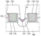
图1是根据本发明实施例的半导体装置1的剖视图。图2A和图2B是图1中示出的金属硅化物151的透视图和剖视图。参照图1,半导体装置1可以包括基底100、栅极116、抬升源极/漏极117、第一层间绝缘膜121、第二层间绝缘膜122、金属硅化物151和金属接触160。1 is a cross-sectional view of a
基底100可以是用于显示器的硅基底、砷化镓基底、硅锗基底、陶瓷基底、石英基底或玻璃基底,或者可以是绝缘体上半导体(semiconductor on insulator,SOI)基底。在下面的描述中,使用硅基底作为示例。The
栅极116形成在基底100上。栅极116可以包括在n沟道金属氧化物半导体(NMOS)晶体管或p沟道金属氧化物半导体(PMOS)晶体管中。栅极116可以具有后栅极结构(gate laststructure)或取代栅极结构(replacement gate structure)。具体地讲,第一层间绝缘膜121包括孔126,栅极116设置在孔126中。The
栅极116可以包括例如第一金属层115和第二金属层110的堆叠。第一金属层115可以沿孔126的侧壁和底表面共形地形成,第二金属层110可以形成在第一金属层115上以填充孔126。第一金属层115可以包含例如TiN,第二金属层110可以包含例如Al。此外,如果栅极116具有后栅极结构,则第一层间绝缘膜121可以低于栅极116。The
抬升源极/漏极117可以形成在栅极116之间。抬升源极/漏极117可以包括形成在基底100中的掺杂区域101和接触掺杂区域101的外延层141。外延层141可以是使用基底100作为基体通过外延方法生长的层。Raised source/
金属硅化物151可以形成在抬升源极/漏极117上。即,抬升源极/漏极117的部分(具体地讲,外延层141)可以包括金属硅化物151。金属硅化物151中使用的金属可以包括Ni、Co、Pt、Ti、W、Hf、Yb、Tb、Dy、Er、Pd和它们的合金中的至少一种。接触孔161穿过第一层间绝缘膜121和第二层间绝缘膜122并暴露金属硅化物151的至少一部分。阻挡层165可以沿接触孔161的侧表面和底表面共形地形成,金属接触160可以形成在阻挡层165上以填充接触孔161。
参照图1和图2,抬升源极/漏极117可以包括突出部分141a,突出部分141a相对于基底100的表面进一步突出并覆盖金属硅化物151的两侧。如附图中所示,随着距基底100的表面的距离增加,突出部分141a可以变得更窄。此外,突出部分141a可以覆盖金属硅化物151的竖直长度(即,高度)的一半以上。在图1中,突出部分141a覆盖金属硅化物151的整个侧表面158。然而,本发明不限于此。Referring to FIGS. 1 and 2 , the raised source/
金属硅化物151可以不形成在抬升源极/漏极117的表面141b的至少一部分中。即,参照图1,抬升源极/漏极117在金属硅化物151与栅极116之间的区域中可以具有未硅化物化的表面。The
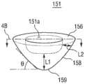
如图2A中所示,金属硅化物151可以包括尖端区域159、侧表面158和上表面156(例如,平坦的上表面156)。金属硅化物151可以具有倒锥形形状,如附图中所示。因此,尖端区域159可以朝下(朝向基底100),上表面156可以朝上(背离基底100)。此外,由于金属硅化物151从底部到顶部变得更宽,所以侧表面158可以以预定角度θ倾斜。预定角度θ可以是但不限于大约30度至大约70度。更具体地讲,预定角度θ可以是但不限于大约40度至大约60度。此外,金属硅化物151的尖端区域159的位置可以比基底100的表面更高。在一些实施例中,尖端区域159比栅极氧化物120更高。在一些实施例中,尖端区域159在栅极氧化物120上方大约15nm或更低的位置。As shown in FIG. 2A, the
如图2A和图2B中进一步所示,金属硅化物151的剖面可以限定远离上表面156的下轮廓152。此外,如图2B中所示,图2A中的金属硅化物151的显著之处在于金属硅化物151的下轮廓152具有弯曲的剖面,并且图2A中的金属硅化物151进一步示出了弯曲剖面的中心部分159可以弯曲。As further shown in FIGS. 2A and 2B , the cross-section of the
如图1中进一步所示,金属硅化物的下轮廓在抬升源极/漏极117中所处水平为:在与直接相邻的栅极116相关的沟道区域的水平上方抬升。在根据本发明的一些实施例中,金属硅化物的下轮廓152所处水平为:在直接相邻的栅极116中可包括的栅极氧化物层120的水平上方抬升。在根据本发明的其他实施例中,金属硅化物的下轮廓152在抬升源极/漏极区域117中的深度大于抬升源极/漏极区域117的总厚度的一半。在根据本发明的其他实施例中,金属硅化物的下轮廓152比直接相邻的栅极116中包括的栅极氧化物层高大约15nm或者更少。As further shown in FIG. 1 , the lower profile of the metal silicide is at a level in the raised source/
可以使用参照图11至图16B描述的工艺来形成金属硅化物151和抬升源极/漏极117。将理解的是,可以将抬升源极/漏极117的至少一部分非晶化(amorphized),非晶化的抬升源极/漏极117可以转变为金属硅化物151。通过这些工艺,金属硅化物151可以呈现倒锥形的大体形状(以提供具有弯曲剖面的下轮廓),金属硅化物151的侧表面158可以以预定角度θ倾斜。
可以通过预非晶化注入(PAI)提供非晶化工艺。具体地讲,非晶化工艺可以是注入Si、Ge、Xe和C中的至少一种的工艺,如图17中所示。因此,金属硅化物151可以包含Si、Ge、Xe和C中的至少一种。例如,半导体装置1可以是NMOS晶体管,外延层141可以是Si,Xe可以用在非晶化工艺中。在这种情况下,金属硅化物151可以包含Si和Xe。在另一示例中,半导体装置1可以是PMOS晶体管,外延层141可以是SiGe,C可以用在非晶化工艺中。在这种情况下,金属硅化物151可以包含Si、Ge和C。The amorphization process can be provided by pre-amorphization implantation (PAI). Specifically, the amorphization process may be a process of implanting at least one of Si, Ge, Xe, and C, as shown in FIG. 17 . Therefore, the
在根据本发明的一些实施例中,半导体装置1可以减小抬升源极/漏极117与金属硅化物151之间的界面电阻。这是由于金属硅化物151的倒锥形形状可以提供金属硅化物151与抬升源极/漏极117之间的宽的接触面积。例如,如果将倒锥形形状的金属硅化物151与传统的平坦(条形形状)的金属硅化物相比,则可以看到,由于金属硅化物151的下轮廓具有弯曲的剖面,所以倒锥形形状的金属硅化物151与抬升源极/漏极117之间的接触面积比平坦的金属硅化物与抬升源极/漏极之间的接触面积宽。此外,金属硅化物151的倒锥形形状可以促进电流的流动。In some embodiments according to the present invention, the
图3是根据本发明的一些实施例中的半导体装置的剖视图。图4A是图3中示出的金属硅化物151的透视图,图4B是图4A中示出的金属硅化物151的剖视图。参照图3以及图4A和图4B,在根据本发明的一些实施例中,金属硅化物151可以具有倒锥形形状,其包括从倒锥形形状的上表面156向尖端区域159凹进的上凹进151a。如在剖视图中所看到的,金属硅化物151的下轮廓的形状可以是弯曲的。3 is a cross-sectional view of a semiconductor device in some embodiments according to the present invention. 4A is a perspective view of the
从上凹进151a的底部到尖端区域159的竖直长度L1可以大于从上凹进151a的侧壁到侧表面158的水平长度L2。这里,竖直长度L1和水平长度L2中的每个是距上凹进151a的边界的长度。由于金属硅化物151沿竖直方向延伸,所以从上凹进151a的底部到尖端区域159的竖直长度L1可以比水平长度L2长。如图4B中所示,金属硅化物151的中心部分159可以具有弯曲的轮廓。The vertical length L1 from the bottom of the
半导体装置2可以是PMOS晶体管。抬升源极/漏极102可以包含SiGe。SiGe层142可形成在基底100中形成的沟槽中。SiGe层142可以是西格玛(Σ)形状。SiGe层142可以将压应力施加到PMOS晶体管,从而提高PMOS晶体管的载流子(空穴)的迁移率。可以通过外延方法形成SiGe层142,以提供包含SiGe的外延层142。The
当Xe和C中的至少一种被用在非晶化工艺中时,金属硅化物151不仅可以包含Si和Ge,还可以包含Xe和C中的至少一种。阻挡层165形成在金属硅化物151上,金属接触160形成在阻挡层165上。金属硅化物151可以围绕阻挡层165的一部分。由于金属硅化物151包括上凹进151a,所以阻挡层165可以形成在上凹进151a中。When at least one of Xe and C is used in the amorphization process, the
如图4A和图4B中所示,金属硅化物151可以具有倒锥形形状,其包括从倒锥形形状的上表面156向尖端区域159凹进的上凹进151a。如在剖视图中所看到的,金属硅化物151的下轮廓的形状可以是弯曲的。As shown in FIGS. 4A and 4B , the
图5是根据本发明的一些实施例中的半导体装置3的剖视图。图6A和图6B分别是图5中示出的金属硅化物151的透视图和剖视图。FIG. 5 is a cross-sectional view of semiconductor device 3 in some embodiments according to the present invention. 6A and 6B are a perspective view and a cross-sectional view, respectively, of the
参照图5以及图6A和图6B,金属硅化物151可以具有倒锥形形状。具体地讲,金属硅化物151可以包括凸状顶部151b,该凸状顶部151b从倒锥形形状的水平平面156向上突出。如附图中所示,凸状顶部151b可以比水平平面156处的宽度窄。凸状顶部151b可以从底部到顶部变得更窄。Referring to FIG. 5 and FIGS. 6A and 6B , the
抬升源极/漏极103可以包含SiC层143,SiC层143形成在基底100中的沟槽中。SiC层143可以将张应力施加到NMOS晶体管,从而提高NMOS晶体管的载流子(电子)的迁移率。可以通过外延方法来形成SiC层143。当Ge和Xe中的至少一种被用在非晶化工艺中时,金属硅化物151不仅可以包含Si和C,还可以包含Ge和Xe中的至少一种。The raised source/
如图6A和图6B中所示,金属硅化物151可以具有倒锥形形状,其包括从倒锥形形状的水平平面156向上突出的凸状顶部151b。如在剖视图中所看到的,金属硅化物151的下轮廓的形状可以是弯曲的。As shown in FIGS. 6A and 6B , the
图7是根据本发明的一些实施例中的半导体装置4的剖视图。在图7中,示出了NMOS晶体管和PMOS晶体管一起形成的情况。参照图7,在基底100中定义了第一区域I和第二区域II。FIG. 7 is a cross-sectional view of
PMOS晶体管可以形成在第一区域I中。PMOS晶体管可以包括第一栅极111、形成在第一栅极111的两侧上的第一抬升源极/漏极102以及形成在第一抬升源极/漏极102上并具有倒锥形形状的第一金属硅化物151。PMOS transistors may be formed in the first region I. The PMOS transistor may include a
NMOS晶体管可以形成在第二区域II中。NMOS晶体管包括第二栅极211、形成在第二栅极211的两侧上的第二抬升源极/漏极201以及形成在第二抬升源极/漏极201上并具有倒锥形形状的第二金属硅化物251。第一金属硅化物151和第二金属硅化物251可以包含相同的材料。这里,所述相同的材料可以包括Ge、Xe和C中的至少一种。NMOS transistors may be formed in the second region II. The NMOS transistor includes a
例如,第一抬升源极/漏极102可以包含SiGe,第二抬升源极/漏极201可以包含Si。在这种情况下,如果Ge用在非晶化工艺中,则Ge不仅可以在第一金属硅化物151中检测到,还可以在第二金属硅化物251中检测到。可选择地,如果Xe用在非晶化工艺中,则第一金属硅化物151和第二金属硅化物251可以包含Xe。For example, the first raised source/
第一金属硅化物151可包括平坦的顶部。如上所述,第一金属硅化物151还可以包括在倒锥形形状的上表面中的向尖端区域凹进的上凹进。此外,第二金属硅化物251还可以包括从倒锥形形状的水平平面向上突出的凸状顶部,该凸状顶部可以比倒锥形形状的水平平面窄。凸状顶部可以从底部向顶部变窄。The
第一金属硅化物151的侧表面可以处于角θ1,角θ1比第二金属硅化物251的侧表面的角θ2大。即,PMOS晶体管的第一金属硅化物151的侧表面可以比NMOS晶体管的第二金属硅化物251的侧表面陡峭。The side surface of the
如上所述,第一抬升源极/漏极102可以包括突出部分,该突出部分相对于基底100的表面进一步突出并覆盖第一金属硅化物151的两侧。随着距基底100的表面的距离增加,突出部分可以变得更窄。第一金属硅化物151可以不形成在第一抬升源极/漏极102的表面的至少一部分中。第一金属硅化物151的倒锥形形状的尖端区域比第一栅极111的沟道区域高。As described above, the first raised source/
第二金属硅化物251的倒锥形形状的尖端区域也可以比第二栅极211的沟道区域高,但不限于此。根据制造工艺,第二金属硅化物251的尖端区域可以与所述沟道区域处于大约相同的水平或者可以比所述沟道区域低。The tip region of the inverted tapered shape of the
基底100上还设置有包括第一孔126和第二孔226的第一层间绝缘膜121。第一栅极111形成在第一孔126中,第二栅极211形成在第二孔226中。此外,第一栅极111包括第一金属层115和第二金属层110,第一金属层115沿第一孔126的侧壁和底表面共形地形成,第二金属层110在第一孔126中形成在第一金属层115上以填充第一孔126。第二栅极211包括第三金属层215和第四金属层210,第三金属层215沿第二孔226的侧壁和底表面共形地形成,第四金属层210在第二孔226中形成在第三金属层215上以填充第二孔226。如附图中所示,第一层间绝缘膜121可以比第一栅极111和第二栅极211低。图5以及图6A和图6B中示出的NMOS晶体管可以形成在第二区域II中。即,可以形成具有包括SiC外延层143的抬升源极/漏极103的NMOS晶体管。A first
图8是根据本发明的一些实施例中的半导体装置5的剖视图。参照图8,基底100包括第一区域I、第二区域II和第三区域III。第一区域I和第二区域II可以分别是存储区域(例如,单元区域(cell region))和逻辑区域(例如,LSI(大规模集成)区域),第三区域III可以是外围区域。例如,外围区域可以包括输入/输出(I/O)区域。与第一区域I和第二区域II相比,第三区域III可以具有更低的密度以及元件之间更宽的间隙。8 is a cross-sectional view of a
PMOS晶体管和NMOS晶体管分别形成在第一区域I和第二区域II中。图5以及图6A和图6B中示出的NMOS晶体管可以形成在第二区域II中。即,可以形成具有包括SiC外延层143的抬升源极/漏极103的NMOS晶体管。PMOS transistors and NMOS transistors are formed in the first region I and the second region II, respectively. The NMOS transistors shown in FIG. 5 and FIGS. 6A and 6B may be formed in the second region II. That is, an NMOS transistor having the raised source/
外延层341可以形成在第三区域III的基底100上,具有倒锥形形状的第三金属硅化物351可以形成在外延层341上。第三金属硅化物351可以设置在相邻的第三栅极311之间。第三抬升源极/漏极301可以比第一抬升源极/漏极102和第二抬升源极/漏极201相对宽。此外,第三金属硅化物351可以比第一金属硅化物151和第二金属硅化物251相对宽。此外,第三金属硅化物351可以包括平坦的顶部。An
图9和图10分别是根据本发明的一些实施例中的半导体装置6的电路图和布局图。根据本发明实施例的半导体装置1至5可应用到使用金属硅化物的所有装置。然而,作为示例,在图9和图10中示出了静态随机存取存储器(SRAM)。9 and 10 are a circuit diagram and a layout diagram, respectively, of a
参照图9,半导体装置6可以包括在电源节点Vcc与接地节点Vss之间并联连接的一对反相器(inverter)INV1和INV2以及分别连接到反相器INV1和INV2的输出节点的第一传输晶体管(transmission transistor)T1和第二传输晶体管T2。第一传输晶体管T1和第二传输晶体管T2可以分别连接到位线BL和互补位线/BL。第一传输晶体管T1和第二传输晶体管T2的栅极可以分别连接到字线WL1和WL2。9 , the
第一反相器INV1包括串联连接的第一负载晶体管(load transistor)T5和第一驱动晶体管T3,第二反相器INV2包括串联连接的第二负载晶体管T6和第二驱动晶体管T4。第一负载晶体管T5和第二负载晶体管T6可以是PMOS晶体管,第一驱动晶体管T3和第二驱动晶体管T4可以是NMOS晶体管。The first inverter INV1 includes a first load transistor T5 and a first drive transistor T3 connected in series, and the second inverter INV2 includes a second load transistor T6 and a second drive transistor T4 connected in series. The first load transistor T5 and the second load transistor T6 may be PMOS transistors, and the first driving transistor T3 and the second driving transistor T4 may be NMOS transistors.
此外,第一反相器INV1的输入节点连接到第二反相器INV2的输出节点(见节点NC2),第二反相器INV2的输入节点连接到第一反相器INV1的输出节点(见节点NC1),从而第一反相器INV1和第二反相器INV2可以形成一个闩锁电路。Further, the input node of the first inverter INV1 is connected to the output node of the second inverter INV2 (see node NC2), and the input node of the second inverter INV2 is connected to the output node of the first inverter INV1 (see the node NC2). node NC1), so that the first inverter INV1 and the second inverter INV2 can form a latch circuit.
参照图9和图10,附图标记410和412表示PMOS晶体管的有源区域,附图标记414和416表示NMOS晶体管的有源区域。附图标记420和422表示第一驱动晶体管T3和第二驱动晶体管T4的栅电极,附图标记430表示第一传输晶体管T1和第二传输晶体管T2的栅电极。附图标记440表示电源线(Vcc线),附图标记450表示接地线(Vss线),附图标记460表示位线BL和互补位线/BL。这里,附图标记490表示金属接触。可以使用上面参照图1至图8描述的根据实施例的半导体装置1至5的金属硅化物和金属接触。9 and 10,
图11至图16B是示出根据本发明的一些实施例中的半导体装置2的制造方法的剖视图。图13B、图14B和图15B是图13A、图14A、图15A的放大剖视图。参照图11,一对晶体管位于基底100上。晶体管分别包括栅极111a/111b以及位于一对栅极111a/111b之间的抬升源极/漏极102。第一层间绝缘膜121覆盖抬升源极/漏极102。形成第二层间绝缘膜122以覆盖抬升源极/漏极102和第一层间绝缘膜121。11 to 16B are cross-sectional views illustrating a method of manufacturing the
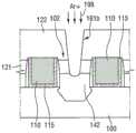
参照图12,通过蚀刻第一层间绝缘膜121和第二层间绝缘膜122来形成接触孔(或开口)161a,以暴露抬升源极/漏极102的表面。在根据本发明的一些实施例中,在第二层间绝缘膜122上形成掩模图案,然后干蚀刻,从而形成接触孔161a。12 , contact holes (or openings) 161 a are formed by etching the first
参照图13A和图13B,执行射频(RF)蚀刻工艺198以减小接触孔161b的尺寸。RF蚀刻工艺198可以使用例如Ar+。RF蚀刻工艺198可以除去形成在抬升源极/漏极102上的天然氧化物膜。此外,RF蚀刻工艺198可以减小接触孔161b的底表面的临界尺寸(CD)。这是由于RF蚀刻工艺198可以使由抬升源极/漏极102、第一层间绝缘膜121和第二层间绝缘膜122产生的蚀刻副产物再次沉积在第一层间绝缘膜121和第二层间绝缘膜122的侧壁上。因此,接触孔161b中的RF蚀刻可以改变接触孔161b的底部处的形状,从而提供在接触孔161b的底部处向暴露的抬升源极/漏极区域102的表面弯曲的弯曲侧壁,以促成例如图13B中示出的形状。在一个实施例中,还可以蚀刻抬升源极/漏极102的表面,以使所述表面的水平凹进。13A and 13B, a radio frequency (RF)
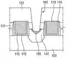
参照图14A和图14B,通过非晶化工艺199对抬升源极/漏极102的至少一部分195非晶化。具体地讲,可以通过预非晶化注入PAI提供抬升源极/漏极102的至少一部分195的非晶化工艺199。非晶化工艺199可以包括注入Si、Ge、Xe和C中的至少一种的工艺。如例如图14B中所示,预非晶化注入可以促成非晶化部分195形成为具有弯曲的下轮廓。此外,非晶化部分195可以具有至少大约100埃的总厚度。将理解的是,预非晶化注入的下轮廓远离直接相邻的抬升源极/漏极区域的表面。Referring to FIGS. 14A and 14B , at least a
图17是示出在抬升源极/漏极区域中形成的非晶硅层的示例性厚度相对于形成在其中的金属硅化物区域的厚度的图。根据图17,与使用诸如C的其他杂质相比,使用Si或Xe可以促成更厚的金属硅化物的形成。17 is a graph showing exemplary thicknesses of amorphous silicon layers formed in raised source/drain regions relative to the thickness of metal silicide regions formed therein. According to FIG. 17, the use of Si or Xe can facilitate the formation of thicker metal silicides compared to the use of other impurities such as C.
参照图15A和图15B,可以执行清洁工艺。具体地讲,可以原位地执行清洁工艺。清洁工艺可以除去形成在抬升源极/漏极102上的天然氧化物膜并调整接触孔161的形状。可以省略清洁工艺。Referring to FIGS. 15A and 15B , a cleaning process may be performed. Specifically, the cleaning process can be performed in situ. The cleaning process may remove the native oxide film formed on the raised source/
参照图16A和图16B,用金属对非晶化抬升源极/漏极102进行硅化物化以形成金属硅化物151。非晶化部分诱使金属硅化物151在硅化物化工艺过程中更多地沿竖直方向生长(参见图16A和图16B)。即,非晶化部分可以促成金属硅化物151形成为遵循与非晶化部分相同的大体倒锥形形状,使得倒锥形形状的下轮廓可以具有弯曲的剖面。金属硅化物151从底部到顶部变得更宽。即,非晶化抬升源极/漏极102的部分195诱使金属硅化物151与沿水平方向相比更多地沿竖直方向生成。Referring to FIGS. 16A and 16B , the amorphized raised source/
可以在非晶化抬升源极/漏极102上形成金属层。例如,金属层可以包含Ni、Co、Pt、Ti、W、Hf、Yb、Tb、Dy、Er、Pd和它们的合金中的至少一种。通过第一热处理使金属层和非晶化抬升源极/漏极102反应。例如,可以在大约200℃至大约540℃的温度下执行第一热处理。此外,第一热处理可以使用快速热退火(RTA)。除去金属层的未反应部分。然后,在比用于第一热处理的温度高的温度下执行第二热处理。例如,可以在大约540℃至大约800℃的温度下执行第二热处理。第二热处理也可以使用RTA。A metal layer may be formed on the amorphized raised source/
如图16A和图16B中所示,非晶化层的硅化物化可以促成金属硅化物生长成为具有下轮廓(远离抬升源极/漏极的表面),所述下轮廓在其中心部分弯曲。因此,在根据本发明的一些实施例中,改变接触孔的底部处的形状可以促成具有弯曲的下轮廓的非晶化层的形成(响应于预非晶化注入),继而可以促成金属硅化物也形成为具有弯曲的剖面轮廓,具体地,在其中心部分的弯曲的剖面轮廓。As shown in FIGS. 16A and 16B , silicidation of the amorphized layer can promote the growth of the metal silicide to have a lower profile (away from the surface of the raised source/drain) that is curved at its central portion. Thus, in some embodiments in accordance with the present invention, changing the shape at the bottom of the contact hole may contribute to the formation of an amorphization layer with a curved lower profile (in response to a pre-amorphization implant), which in turn may contribute to metal silicide It is also formed to have a curved cross-sectional profile, specifically, a curved cross-sectional profile at its central portion.
往回参照图3,沿接触孔161的侧表面和底表面共形地形成阻挡层165。此外,在阻挡层165上形成金属接触160以填充接触孔161。Referring back to FIG. 3 , the
虽然已参照示例实施例描述了本发明构思,但对本领域技术人员将明显的是,在不脱离本发明构思的精神和范围的情况下,可以做出各种改变和修改。因此,应该理解的是,以上实施例不是限制,而是说明性的。因此,本发明构思的范围将由权利要求书及其等同物的最宽泛的允许的解释来确定,而不应该受前面的描述的约束或限制。Although the inventive concept has been described with reference to example embodiments, it will be apparent to those skilled in the art that various changes and modifications can be made without departing from the spirit and scope of the inventive concept. Therefore, it should be understood that the above embodiments are not limiting, but illustrative. Therefore, the scope of the inventive concept is to be determined by the broadest permissible interpretation of the claims and their equivalents, and shall not be restricted or limited by the foregoing description.
Claims (8)
Translated fromChineseApplications Claiming Priority (3)
| Application Number | Priority Date | Filing Date | Title |
|---|---|---|---|
| KR1020120055543AKR101952119B1 (en) | 2012-05-24 | 2012-05-24 | Semiconductor device using metal silicide and fabricating method thereof |
| KR10-2012-0055543 | 2012-05-24 | ||
| CN201310195386.1ACN103426739B (en) | 2012-05-24 | 2013-05-23 | Method of forming semiconductor device using pre-amorphization implantation and formed device |
Related Parent Applications (1)
| Application Number | Title | Priority Date | Filing Date |
|---|---|---|---|
| CN201310195386.1ADivisionCN103426739B (en) | 2012-05-24 | 2013-05-23 | Method of forming semiconductor device using pre-amorphization implantation and formed device |
Publications (2)
| Publication Number | Publication Date |
|---|---|
| CN106898545A CN106898545A (en) | 2017-06-27 |
| CN106898545Btrue CN106898545B (en) | 2020-02-18 |
Family
ID=49621927
Family Applications (2)
| Application Number | Title | Priority Date | Filing Date |
|---|---|---|---|
| CN201310195386.1AActiveCN103426739B (en) | 2012-05-24 | 2013-05-23 | Method of forming semiconductor device using pre-amorphization implantation and formed device |
| CN201710130527.XAActiveCN106898545B (en) | 2012-05-24 | 2013-05-23 | semiconductor device |
Family Applications Before (1)
| Application Number | Title | Priority Date | Filing Date |
|---|---|---|---|
| CN201310195386.1AActiveCN103426739B (en) | 2012-05-24 | 2013-05-23 | Method of forming semiconductor device using pre-amorphization implantation and formed device |
Country Status (4)
| Country | Link |
|---|---|
| US (3) | US9240323B2 (en) |
| KR (1) | KR101952119B1 (en) |
| CN (2) | CN103426739B (en) |
| TW (1) | TWI591690B (en) |
Families Citing this family (37)
| Publication number | Priority date | Publication date | Assignee | Title |
|---|---|---|---|---|
| US9601619B2 (en) | 2013-07-16 | 2017-03-21 | Taiwan Semiconductor Manufacturing Company, Ltd. | MOS devices with non-uniform P-type impurity profile |
| US9583483B2 (en)* | 2013-09-03 | 2017-02-28 | Taiwan Semiconductor Manufacturing Company, Ltd. | Source and drain stressors with recessed top surfaces |
| US9231098B2 (en)* | 2013-10-30 | 2016-01-05 | Taiwan Semiconductor Manufacturing Co., Ltd. | Mechanism for forming metal gate structure |
| US9508601B2 (en) | 2013-12-12 | 2016-11-29 | Texas Instruments Incorporated | Method to form silicide and contact at embedded epitaxial facet |
| US10032876B2 (en)* | 2014-03-13 | 2018-07-24 | Taiwan Semiconductor Manufacturing Company, Ltd. | Contact silicide having a non-angular profile |
| US10084063B2 (en)* | 2014-06-23 | 2018-09-25 | Taiwan Semiconductor Manufacturing Company Ltd. | Semiconductor device and manufacturing method thereof |
| KR102230198B1 (en)* | 2014-09-23 | 2021-03-19 | 삼성전자주식회사 | Semiconductor device and method for manufacturing the same |
| KR102246880B1 (en)* | 2015-02-10 | 2021-04-30 | 삼성전자 주식회사 | Integrated circuit device and method of manufacturing the same |
| US9691804B2 (en)* | 2015-04-17 | 2017-06-27 | Taiwan Semiconductor Manufacturing Company Ltd. | Image sensing device and manufacturing method thereof |
| US9947753B2 (en) | 2015-05-15 | 2018-04-17 | Taiwan Semiconductor Manufacturing Co., Ltd. | Semiconductor structure and manufacturing method thereof |
| US9484431B1 (en)* | 2015-07-29 | 2016-11-01 | International Business Machines Corporation | Pure boron for silicide contact |
| TWI682547B (en) | 2015-10-06 | 2020-01-11 | 聯華電子股份有限公司 | Semiconductor structure and manufacturing method thereof |
| US9871042B2 (en) | 2015-12-03 | 2018-01-16 | Samsung Electronics Co., Ltd. | Semiconductor device having fin-type patterns |
| US9722081B1 (en)* | 2016-01-29 | 2017-08-01 | Taiwan Semiconductor Manufacturing Co., Ltd. | FinFET device and method of forming the same |
| US10153351B2 (en) | 2016-01-29 | 2018-12-11 | Taiwan Semiconductor Manufacturing Co., Ltd. | Semiconductor device and a method for fabricating the same |
| CN107104051B (en)* | 2016-02-22 | 2021-06-29 | 联华电子股份有限公司 | Semiconductor device and method of making the same |
| US10304743B2 (en)* | 2016-06-02 | 2019-05-28 | Toshiba Memory Corporation | Semiconductor device and manufacturing method thereof |
| CN108122824B (en)* | 2016-11-30 | 2020-12-22 | 中芯国际集成电路制造(上海)有限公司 | Semiconductor structure and forming method thereof |
| US10163643B2 (en)* | 2016-12-14 | 2018-12-25 | Taiwan Semiconductor Manufacturing Company, Ltd. | Method of forming semiconductor device using titanium-containing layer and device formed |
| US10468300B2 (en)* | 2017-07-05 | 2019-11-05 | Globalfoundries Inc. | Contacting source and drain of a transistor device |
| CN109599337A (en)* | 2017-09-30 | 2019-04-09 | 中芯国际集成电路制造(上海)有限公司 | Semiconductor devices and forming method thereof |
| CN109817713B (en)* | 2017-11-22 | 2022-04-15 | 中芯国际集成电路制造(上海)有限公司 | Semiconductor device and method of forming the same |
| US10535748B2 (en)* | 2018-03-01 | 2020-01-14 | Taiwan Semiconductor Manufacturing Co., Ltd. | Method of forming a contact with a silicide region |
| US11145751B2 (en)* | 2018-03-29 | 2021-10-12 | Taiwan Semiconductor Manufacturing Co., Ltd. | Semiconductor structure with doped contact plug and method for forming the same |
| KR102481414B1 (en)* | 2018-07-05 | 2022-12-23 | 어플라이드 머티어리얼스, 인코포레이티드 | Silicide film nucleation |
| US10573725B1 (en)* | 2018-09-20 | 2020-02-25 | Nanya Technology Corporation | Semiconductor structure and manufacturing method thereof |
| FR3086796A1 (en)* | 2018-09-28 | 2020-04-03 | Stmicroelectronics (Crolles 2) Sas | SILICIURATION PROCESS |
| US11626505B2 (en)* | 2019-06-27 | 2023-04-11 | Taiwan Semiconductor Manufacturing Co., Ltd. | Dielectric inner spacers in multi-gate field-effect transistors |
| CN112151613A (en) | 2019-06-27 | 2020-12-29 | 台湾积体电路制造股份有限公司 | semiconductor structure |
| CN112151607B (en)* | 2019-06-28 | 2023-08-08 | 中芯国际集成电路制造(上海)有限公司 | Semiconductor structure and forming method thereof |
| CN113130516A (en)* | 2020-01-15 | 2021-07-16 | 联华电子股份有限公司 | Semiconductor image sensing element and manufacturing method thereof |
| US11189565B2 (en) | 2020-02-19 | 2021-11-30 | Nanya Technology Corporation | Semiconductor device with programmable anti-fuse feature and method for fabricating the same |
| TWI730769B (en) | 2020-05-19 | 2021-06-11 | 力晶積成電子製造股份有限公司 | Manufacturing method of semiconductor device |
| US12266572B2 (en)* | 2020-08-13 | 2025-04-01 | Taiwan Semiconductor Manufacturing Co., Ltd. | Embedded stressors in epitaxy source/drain regions |
| KR20220108613A (en) | 2021-01-27 | 2022-08-03 | 삼성전자주식회사 | Integrated circuit device |
| JP2023076275A (en)* | 2021-11-22 | 2023-06-01 | シャープディスプレイテクノロジー株式会社 | Active matrix substrate and liquid crystal display device |
| US20230402278A1 (en)* | 2022-06-12 | 2023-12-14 | Taiwan Semiconductor Manufacturing Company, Ltd. | Semiconductor devices and methods of forming the same |
Citations (2)
| Publication number | Priority date | Publication date | Assignee | Title |
|---|---|---|---|---|
| CN102110689A (en)* | 2009-12-29 | 2011-06-29 | 中国科学院微电子研究所 | Semiconductor device and manufacturing method thereof |
| CN102437088A (en)* | 2010-09-29 | 2012-05-02 | 中国科学院微电子研究所 | Semiconductor structure and manufacturing method thereof |
Family Cites Families (31)
| Publication number | Priority date | Publication date | Assignee | Title |
|---|---|---|---|---|
| JPH10242081A (en)* | 1996-12-26 | 1998-09-11 | Sony Corp | Manufacture of semiconductor device |
| US6569746B2 (en)* | 1997-10-30 | 2003-05-27 | Samsung Electronics Co., Ltd. | Methods of forming integrated circuit capacitors having electrodes therein that comprise conductive plugs |
| US6518626B1 (en)* | 2000-02-22 | 2003-02-11 | Micron Technology, Inc. | Method of forming low dielectric silicon oxynitride spacer films highly selective of etchants |
| KR100350811B1 (en)* | 2000-08-19 | 2002-09-05 | 삼성전자 주식회사 | Metal Via Contact of Semiconductor Devices and Method of Forming it |
| US7646544B2 (en)* | 2005-05-14 | 2010-01-12 | Batchko Robert G | Fluidic optical devices |
| US7256112B2 (en) | 2005-01-20 | 2007-08-14 | Chartered Semiconductor Manufacturing, Ltd | Laser activation of implanted contact plug for memory bitline fabrication |
| JP5118300B2 (en)* | 2005-12-20 | 2013-01-16 | 富士通セミコンダクター株式会社 | Semiconductor device and manufacturing method thereof |
| WO2007139781A2 (en)* | 2006-05-23 | 2007-12-06 | Cree Led Lighting Solutions, Inc. | Lighting device |
| KR100809330B1 (en)* | 2006-09-04 | 2008-03-05 | 삼성전자주식회사 | Semiconductor Device Eliminating Stress Due to Gate Spacer and Manufacturing Method Thereof |
| US7625801B2 (en)* | 2006-09-19 | 2009-12-01 | Taiwan Semiconductor Manufacturing Company, Ltd. | Silicide formation with a pre-amorphous implant |
| US7968952B2 (en)* | 2006-12-29 | 2011-06-28 | Intel Corporation | Stressed barrier plug slot contact structure for transistor performance enhancement |
| US20080206973A1 (en)* | 2007-02-26 | 2008-08-28 | Texas Instrument Inc. | Process method to optimize fully silicided gate (FUSI) thru PAI implant |
| US20090050972A1 (en) | 2007-08-20 | 2009-02-26 | Richard Lindsay | Strained Semiconductor Device and Method of Making Same |
| KR20090068468A (en)* | 2007-12-24 | 2009-06-29 | 주식회사 동부하이텍 | Method of fabricating semiconductor cevice |
| DE102008011814B4 (en) | 2008-02-29 | 2012-04-26 | Advanced Micro Devices, Inc. | CMOS device with buried insulating layer and deformed channel regions and method for producing the same |
| DE102008030854B4 (en)* | 2008-06-30 | 2014-03-20 | Advanced Micro Devices, Inc. | MOS transistors having depressed drain and source regions and non-conforming metal silicide regions, and methods of fabricating the transistors |
| US20100109046A1 (en)* | 2008-11-03 | 2010-05-06 | Rishabh Mehandru | Methods of forming low interface resistance contacts and structures formed thereby |
| US8778708B2 (en)* | 2009-03-06 | 2014-07-15 | E I Du Pont De Nemours And Company | Process for forming an electroactive layer |
| JP2011009645A (en) | 2009-06-29 | 2011-01-13 | Toshiba Corp | Semiconductor device and method of manufacturing the same |
| US8900674B2 (en)* | 2009-10-06 | 2014-12-02 | Tel Solar Ag | Method of coating a substrate |
| JP5734688B2 (en)* | 2010-02-10 | 2015-06-17 | キヤノン株式会社 | Method for producing oriented oxide ceramics, oriented oxide ceramics, piezoelectric element, liquid discharge head, ultrasonic motor, and dust removing device |
| US20120080070A1 (en)* | 2010-09-30 | 2012-04-05 | General Electric Company | Photovoltaic devices |
| KR101716113B1 (en)* | 2010-11-03 | 2017-03-15 | 삼성전자 주식회사 | Semiconductor device and method of manufacturing thereof |
| CN102487014B (en)* | 2010-12-03 | 2014-03-05 | 中国科学院微电子研究所 | Semiconductor structure and manufacturing method thereof |
| US8598646B2 (en)* | 2011-01-13 | 2013-12-03 | Spansion Llc | Non-volatile FINFET memory array and manufacturing method thereof |
| US8652914B2 (en)* | 2011-03-03 | 2014-02-18 | International Business Machines Corporation | Two-step silicide formation |
| US8445347B2 (en)* | 2011-04-11 | 2013-05-21 | Sandisk Technologies Inc. | 3D vertical NAND and method of making thereof by front and back side processing |
| US8415250B2 (en)* | 2011-04-29 | 2013-04-09 | International Business Machines Corporation | Method of forming silicide contacts of different shapes selectively on regions of a semiconductor device |
| US20120313149A1 (en)* | 2011-06-09 | 2012-12-13 | Beijing Nmc Co., Ltd. | Semiconductor structure and method for manufacturing the same |
| US8377769B2 (en)* | 2011-06-30 | 2013-02-19 | Institute of Microelectronics, Chinese Academy of Sciences | Method for integrating replacement gate in semiconductor device |
| US8975672B2 (en)* | 2011-11-09 | 2015-03-10 | United Microelectronics Corp. | Metal oxide semiconductor transistor and manufacturing method thereof |
- 2012
- 2012-05-24KRKR1020120055543Apatent/KR101952119B1/enactiveActive
- 2013
- 2013-03-07USUS13/788,599patent/US9240323B2/enactiveActive
- 2013-05-22TWTW102117973Apatent/TWI591690B/enactive
- 2013-05-23CNCN201310195386.1Apatent/CN103426739B/enactiveActive
- 2013-05-23CNCN201710130527.XApatent/CN106898545B/enactiveActive
- 2015
- 2015-12-09USUS14/963,731patent/US10043902B2/enactiveActive
- 2018
- 2018-07-03USUS16/026,614patent/US10840374B2/enactiveActive
Patent Citations (2)
| Publication number | Priority date | Publication date | Assignee | Title |
|---|---|---|---|---|
| CN102110689A (en)* | 2009-12-29 | 2011-06-29 | 中国科学院微电子研究所 | Semiconductor device and manufacturing method thereof |
| CN102437088A (en)* | 2010-09-29 | 2012-05-02 | 中国科学院微电子研究所 | Semiconductor structure and manufacturing method thereof |
Also Published As
| Publication number | Publication date |
|---|---|
| US10043902B2 (en) | 2018-08-07 |
| US10840374B2 (en) | 2020-11-17 |
| CN103426739B (en) | 2017-12-22 |
| US20130316535A1 (en) | 2013-11-28 |
| CN106898545A (en) | 2017-06-27 |
| TWI591690B (en) | 2017-07-11 |
| KR101952119B1 (en) | 2019-02-28 |
| US20180331218A1 (en) | 2018-11-15 |
| TW201403677A (en) | 2014-01-16 |
| US9240323B2 (en) | 2016-01-19 |
| CN103426739A (en) | 2013-12-04 |
| KR20130131755A (en) | 2013-12-04 |
| US20160233334A1 (en) | 2016-08-11 |
Similar Documents
| Publication | Publication Date | Title |
|---|---|---|
| CN106898545B (en) | semiconductor device | |
| CN111092112B (en) | MOS field effect transistor and method of making the same | |
| JP4889901B2 (en) | Method for forming source / drain regions having deep junctions | |
| JP5172083B2 (en) | Semiconductor device, manufacturing method thereof, and memory circuit | |
| US9472466B2 (en) | Semiconductor device having reduced-damage active region and method of manufacturing the same | |
| CN107799422B (en) | Method of forming semiconductor device | |
| CN103137685B (en) | Semiconductor device and manufacture method thereof | |
| CN101361178B (en) | Semiconductor transistors with expanded top portions of gates | |
| US8853008B1 (en) | Counter-doped low-power FinFET | |
| TW200536122A (en) | Finfet transistor device on soi and method of fabrication | |
| US7964921B2 (en) | MOSFET and production method of semiconductor device | |
| TWI782101B (en) | Semiconductor structure and fabrication method thereof | |
| US8878301B2 (en) | Semiconductor device with transistors having different source/drain region depths | |
| CN102693916A (en) | Method for improving thermal stability of metal-oxide-semiconductor field effect transistors (MOSFETs) nickel-based silicide | |
| CN1830073B (en) | FET with doped gate electrode to reduce gate depletion and method of forming same | |
| US7049218B2 (en) | Method of fabricating local interconnection using selective epitaxial growth | |
| JP5503833B2 (en) | MOS transistor, semiconductor device and manufacturing method thereof | |
| TWI790476B (en) | Integrated circuit die and method of manufacturing the same | |
| KR20090056429A (en) | Semiconductor device and manufacturing method thereof | |
| JP5657601B2 (en) | Semiconductor device and manufacturing method thereof | |
| CN119698048A (en) | Transistor structure with multiple vertical thin bodies | |
| CN106935490B (en) | Semiconductor device, preparation method thereof and electronic device | |
| TW402745B (en) | Manufacture of salicide | |
| TW518677B (en) | Manufacturing method of metal gate transistor | |
| CN117766395A (en) | Method for manufacturing semiconductor device |
Legal Events
| Date | Code | Title | Description |
|---|---|---|---|
| PB01 | Publication | ||
| PB01 | Publication | ||
| SE01 | Entry into force of request for substantive examination | ||
| GR01 | Patent grant | ||
| GR01 | Patent grant |