CN106887453B - Group III-N Nanowire Transistors - Google Patents
Group III-N Nanowire TransistorsDownload PDFInfo
- Publication number
- CN106887453B CN106887453BCN201710025642.0ACN201710025642ACN106887453BCN 106887453 BCN106887453 BCN 106887453BCN 201710025642 ACN201710025642 ACN 201710025642ACN 106887453 BCN106887453 BCN 106887453B
- Authority
- CN
- China
- Prior art keywords
- group iii
- nanowire
- vertically stacked
- nanowires
- channel region
- Prior art date
- Legal status (The legal status is an assumption and is not a legal conclusion. Google has not performed a legal analysis and makes no representation as to the accuracy of the status listed.)
- Active
Links
- 239000002070nanowireSubstances0.000titleclaimsabstractdescription194
- 239000000463materialSubstances0.000claimsabstractdescription114
- 239000000758substrateSubstances0.000claimsabstractdescription37
- 239000004020conductorSubstances0.000claimsabstractdescription17
- 239000012212insulatorSubstances0.000claimsabstract3
- 239000004065semiconductorSubstances0.000claimsdescription129
- 238000000034methodMethods0.000claimsdescription28
- 239000013078crystalSubstances0.000claimsdescription19
- 229910052984zinc sulfideInorganic materials0.000claimsdescription7
- 229910045601alloyInorganic materials0.000claimsdescription6
- 239000000956alloySubstances0.000claimsdescription6
- 238000004519manufacturing processMethods0.000claimsdescription6
- 230000008878couplingEffects0.000claimsdescription3
- 238000010168coupling processMethods0.000claimsdescription3
- 238000005859coupling reactionMethods0.000claimsdescription3
- 239000002131composite materialSubstances0.000claimsdescription2
- 229910016920AlzGa1−zInorganic materials0.000claims3
- 238000004347surface barrierMethods0.000claims2
- 230000010355oscillationEffects0.000claims1
- 230000001939inductive effectEffects0.000abstractdescription9
- 230000004888barrier functionEffects0.000abstractdescription8
- 239000010410layerSubstances0.000description133
- 229910002601GaNInorganic materials0.000description15
- 230000010287polarizationEffects0.000description15
- 150000004767nitridesChemical class0.000description10
- 230000006870functionEffects0.000description9
- 229910052710siliconInorganic materials0.000description8
- 239000010703siliconSubstances0.000description8
- XUIMIQQOPSSXEZ-UHFFFAOYSA-NSiliconChemical compound[Si]XUIMIQQOPSSXEZ-UHFFFAOYSA-N0.000description7
- 238000004891communicationMethods0.000description7
- 238000010586diagramMethods0.000description7
- 239000011229interlayerSubstances0.000description7
- IJGRMHOSHXDMSA-UHFFFAOYSA-NAtomic nitrogenChemical compoundN#NIJGRMHOSHXDMSA-UHFFFAOYSA-N0.000description6
- NWAIGJYBQQYSPW-UHFFFAOYSA-NazanylidyneindiganeChemical compound[In]#NNWAIGJYBQQYSPW-UHFFFAOYSA-N0.000description6
- 238000005516engineering processMethods0.000description6
- 230000008569processEffects0.000description6
- 230000005540biological transmissionEffects0.000description5
- 239000003989dielectric materialSubstances0.000description5
- 230000000694effectsEffects0.000description5
- 230000002269spontaneous effectEffects0.000description5
- 238000000137annealingMethods0.000description4
- 239000002800charge carrierSubstances0.000description4
- 239000000203mixtureSubstances0.000description4
- PXHVJJICTQNCMI-UHFFFAOYSA-NNickelChemical compound[Ni]PXHVJJICTQNCMI-UHFFFAOYSA-N0.000description3
- KDLHZDBZIXYQEI-UHFFFAOYSA-NPalladiumChemical compound[Pd]KDLHZDBZIXYQEI-UHFFFAOYSA-N0.000description3
- 229910052782aluminiumInorganic materials0.000description3
- 230000003321amplificationEffects0.000description3
- 238000006243chemical reactionMethods0.000description3
- 238000005229chemical vapour depositionMethods0.000description3
- 239000012535impuritySubstances0.000description3
- 230000010354integrationEffects0.000description3
- 229910052751metalInorganic materials0.000description3
- 239000002184metalSubstances0.000description3
- 238000001465metallisationMethods0.000description3
- 229910052757nitrogenInorganic materials0.000description3
- 238000003199nucleic acid amplification methodMethods0.000description3
- BASFCYQUMIYNBI-UHFFFAOYSA-NplatinumChemical compound[Pt]BASFCYQUMIYNBI-UHFFFAOYSA-N0.000description3
- 238000012545processingMethods0.000description3
- 125000006850spacer groupChemical group0.000description3
- JBRZTFJDHDCESZ-UHFFFAOYSA-NAsGaChemical compound[As]#[Ga]JBRZTFJDHDCESZ-UHFFFAOYSA-N0.000description2
- 229910001218Gallium arsenideInorganic materials0.000description2
- 238000000231atomic layer depositionMethods0.000description2
- 230000033228biological regulationEffects0.000description2
- 230000015572biosynthetic processEffects0.000description2
- 230000015556catabolic processEffects0.000description2
- 238000000151depositionMethods0.000description2
- 230000008021depositionEffects0.000description2
- 238000011982device technologyMethods0.000description2
- 238000005530etchingMethods0.000description2
- 230000005669field effectEffects0.000description2
- 229910052733galliumInorganic materials0.000description2
- 229910052732germaniumInorganic materials0.000description2
- GNPVGFCGXDBREM-UHFFFAOYSA-Ngermanium atomChemical compound[Ge]GNPVGFCGXDBREM-UHFFFAOYSA-N0.000description2
- 239000010931goldSubstances0.000description2
- 238000002248hydride vapour-phase epitaxyMethods0.000description2
- 238000000206photolithographyMethods0.000description2
- 238000001020plasma etchingMethods0.000description2
- 229910002059quaternary alloyInorganic materials0.000description2
- 229910002058ternary alloyInorganic materials0.000description2
- 239000010936titaniumSubstances0.000description2
- 229910017121AlSiOInorganic materials0.000description1
- OKTJSMMVPCPJKN-UHFFFAOYSA-NCarbonChemical compound[C]OKTJSMMVPCPJKN-UHFFFAOYSA-N0.000description1
- 229910004143HfONInorganic materials0.000description1
- -1HfSiOChemical class0.000description1
- 229910004129HfSiOInorganic materials0.000description1
- 229910000673Indium arsenideInorganic materials0.000description1
- GPXJNWSHGFTCBW-UHFFFAOYSA-NIndium phosphideChemical compound[In]#PGPXJNWSHGFTCBW-UHFFFAOYSA-N0.000description1
- ZOKXTWBITQBERF-UHFFFAOYSA-NMolybdenumChemical compound[Mo]ZOKXTWBITQBERF-UHFFFAOYSA-N0.000description1
- KJTLSVCANCCWHF-UHFFFAOYSA-NRutheniumChemical compound[Ru]KJTLSVCANCCWHF-UHFFFAOYSA-N0.000description1
- 229910052581Si3N4Inorganic materials0.000description1
- RTAQQCXQSZGOHL-UHFFFAOYSA-NTitaniumChemical compound[Ti]RTAQQCXQSZGOHL-UHFFFAOYSA-N0.000description1
- XAGFODPZIPBFFR-UHFFFAOYSA-NaluminiumChemical compound[Al]XAGFODPZIPBFFR-UHFFFAOYSA-N0.000description1
- RNQKDQAVIXDKAG-UHFFFAOYSA-Naluminum galliumChemical compound[Al].[Ga]RNQKDQAVIXDKAG-UHFFFAOYSA-N0.000description1
- AJGDITRVXRPLBY-UHFFFAOYSA-Naluminum indiumChemical compound[Al].[In]AJGDITRVXRPLBY-UHFFFAOYSA-N0.000description1
- 229910052799carbonInorganic materials0.000description1
- 230000010267cellular communicationEffects0.000description1
- 150000001875compoundsChemical class0.000description1
- 238000002425crystallisationMethods0.000description1
- 230000008025crystallizationEffects0.000description1
- 230000007547defectEffects0.000description1
- 238000009826distributionMethods0.000description1
- 230000005684electric fieldEffects0.000description1
- 238000011049fillingMethods0.000description1
- CMIHHWBVHJVIGI-UHFFFAOYSA-Ngadolinium(iii) oxideChemical compound[O-2].[O-2].[O-2].[Gd+3].[Gd+3]CMIHHWBVHJVIGI-UHFFFAOYSA-N0.000description1
- VTGARNNDLOTBET-UHFFFAOYSA-Ngallium antimonideChemical compound[Sb]#[Ga]VTGARNNDLOTBET-UHFFFAOYSA-N0.000description1
- PCHJSUWPFVWCPO-UHFFFAOYSA-NgoldChemical compound[Au]PCHJSUWPFVWCPO-UHFFFAOYSA-N0.000description1
- 229910052737goldInorganic materials0.000description1
- CJNBYAVZURUTKZ-UHFFFAOYSA-Nhafnium(iv) oxideChemical compoundO=[Hf]=OCJNBYAVZURUTKZ-UHFFFAOYSA-N0.000description1
- WPYVAWXEWQSOGY-UHFFFAOYSA-Nindium antimonideChemical compound[Sb]#[In]WPYVAWXEWQSOGY-UHFFFAOYSA-N0.000description1
- RPQDHPTXJYYUPQ-UHFFFAOYSA-Nindium arsenideChemical compound[In]#[As]RPQDHPTXJYYUPQ-UHFFFAOYSA-N0.000description1
- 229910052741iridiumInorganic materials0.000description1
- GKOZUEZYRPOHIO-UHFFFAOYSA-Niridium atomChemical compound[Ir]GKOZUEZYRPOHIO-UHFFFAOYSA-N0.000description1
- 238000002955isolationMethods0.000description1
- 230000007774longtermEffects0.000description1
- 150000001247metal acetylidesChemical class0.000description1
- 238000004377microelectronicMethods0.000description1
- 238000012986modificationMethods0.000description1
- 230000004048modificationEffects0.000description1
- 238000001451molecular beam epitaxyMethods0.000description1
- 229910052750molybdenumInorganic materials0.000description1
- 239000011733molybdenumSubstances0.000description1
- 229910052759nickelInorganic materials0.000description1
- 229910052763palladiumInorganic materials0.000description1
- 238000002161passivationMethods0.000description1
- 229910052697platinumInorganic materials0.000description1
- 229910021420polycrystalline siliconInorganic materials0.000description1
- 229920005591polysiliconPolymers0.000description1
- 239000002243precursorSubstances0.000description1
- 229910052707rutheniumInorganic materials0.000description1
- 229910052594sapphireInorganic materials0.000description1
- 239000010980sapphireSubstances0.000description1
- 150000004760silicatesChemical class0.000description1
- 229910021332silicideInorganic materials0.000description1
- HQVNEWCFYHHQES-UHFFFAOYSA-Nsilicon nitrideChemical compoundN12[Si]34N5[Si]62N3[Si]51N64HQVNEWCFYHHQES-UHFFFAOYSA-N0.000description1
- 239000007787solidSubstances0.000description1
- 238000003860storageMethods0.000description1
- 238000006467substitution reactionMethods0.000description1
- 229910052715tantalumInorganic materials0.000description1
- GUVRBAGPIYLISA-UHFFFAOYSA-Ntantalum atomChemical compound[Ta]GUVRBAGPIYLISA-UHFFFAOYSA-N0.000description1
- OCGWQDWYSQAFTO-UHFFFAOYSA-NtellanylideneleadChemical compound[Pb]=[Te]OCGWQDWYSQAFTO-UHFFFAOYSA-N0.000description1
- 229910052719titaniumInorganic materials0.000description1
- WFKWXMTUELFFGS-UHFFFAOYSA-NtungstenChemical compound[W]WFKWXMTUELFFGS-UHFFFAOYSA-N0.000description1
- 229910052721tungstenInorganic materials0.000description1
- 239000010937tungstenSubstances0.000description1
- 230000005533two-dimensional electron gasEffects0.000description1
- 238000003631wet chemical etchingMethods0.000description1
- 238000004804windingMethods0.000description1
Images


Classifications
- H—ELECTRICITY
- H10—SEMICONDUCTOR DEVICES; ELECTRIC SOLID-STATE DEVICES NOT OTHERWISE PROVIDED FOR
- H10D—INORGANIC ELECTRIC SEMICONDUCTOR DEVICES
- H10D62/00—Semiconductor bodies, or regions thereof, of devices having potential barriers
- H10D62/80—Semiconductor bodies, or regions thereof, of devices having potential barriers characterised by the materials
- H10D62/81—Semiconductor bodies, or regions thereof, of devices having potential barriers characterised by the materials of structures exhibiting quantum-confinement effects, e.g. single quantum wells; of structures having periodic or quasi-periodic potential variation
- H10D62/815—Semiconductor bodies, or regions thereof, of devices having potential barriers characterised by the materials of structures exhibiting quantum-confinement effects, e.g. single quantum wells; of structures having periodic or quasi-periodic potential variation of structures having periodic or quasi-periodic potential variation, e.g. superlattices or multiple quantum wells [MQW]
- H10D62/8181—Structures having no potential periodicity in the vertical direction, e.g. lateral superlattices or lateral surface superlattices [LSS]
- B—PERFORMING OPERATIONS; TRANSPORTING
- B82—NANOTECHNOLOGY
- B82Y—SPECIFIC USES OR APPLICATIONS OF NANOSTRUCTURES; MEASUREMENT OR ANALYSIS OF NANOSTRUCTURES; MANUFACTURE OR TREATMENT OF NANOSTRUCTURES
- B82Y10/00—Nanotechnology for information processing, storage or transmission, e.g. quantum computing or single electron logic
- H—ELECTRICITY
- H01—ELECTRIC ELEMENTS
- H01L—SEMICONDUCTOR DEVICES NOT COVERED BY CLASS H10
- H01L23/00—Details of semiconductor or other solid state devices
- H01L23/58—Structural electrical arrangements for semiconductor devices not otherwise provided for, e.g. in combination with batteries
- H01L23/64—Impedance arrangements
- H01L23/66—High-frequency adaptations
- H—ELECTRICITY
- H10—SEMICONDUCTOR DEVICES; ELECTRIC SOLID-STATE DEVICES NOT OTHERWISE PROVIDED FOR
- H10D—INORGANIC ELECTRIC SEMICONDUCTOR DEVICES
- H10D30/00—Field-effect transistors [FET]
- H10D30/01—Manufacture or treatment
- H10D30/014—Manufacture or treatment of FETs having zero-dimensional [0D] or one-dimensional [1D] channels, e.g. quantum wire FETs, single-electron transistors [SET] or Coulomb blockade transistors
- H—ELECTRICITY
- H10—SEMICONDUCTOR DEVICES; ELECTRIC SOLID-STATE DEVICES NOT OTHERWISE PROVIDED FOR
- H10D—INORGANIC ELECTRIC SEMICONDUCTOR DEVICES
- H10D30/00—Field-effect transistors [FET]
- H10D30/01—Manufacture or treatment
- H10D30/015—Manufacture or treatment of FETs having heterojunction interface channels or heterojunction gate electrodes, e.g. HEMT
- H—ELECTRICITY
- H10—SEMICONDUCTOR DEVICES; ELECTRIC SOLID-STATE DEVICES NOT OTHERWISE PROVIDED FOR
- H10D—INORGANIC ELECTRIC SEMICONDUCTOR DEVICES
- H10D30/00—Field-effect transistors [FET]
- H10D30/01—Manufacture or treatment
- H10D30/021—Manufacture or treatment of FETs having insulated gates [IGFET]
- H10D30/031—Manufacture or treatment of FETs having insulated gates [IGFET] of thin-film transistors [TFT]
- H—ELECTRICITY
- H10—SEMICONDUCTOR DEVICES; ELECTRIC SOLID-STATE DEVICES NOT OTHERWISE PROVIDED FOR
- H10D—INORGANIC ELECTRIC SEMICONDUCTOR DEVICES
- H10D30/00—Field-effect transistors [FET]
- H10D30/40—FETs having zero-dimensional [0D], one-dimensional [1D] or two-dimensional [2D] charge carrier gas channels
- H10D30/43—FETs having zero-dimensional [0D], one-dimensional [1D] or two-dimensional [2D] charge carrier gas channels having 1D charge carrier gas channels, e.g. quantum wire FETs or transistors having 1D quantum-confined channels
- H—ELECTRICITY
- H10—SEMICONDUCTOR DEVICES; ELECTRIC SOLID-STATE DEVICES NOT OTHERWISE PROVIDED FOR
- H10D—INORGANIC ELECTRIC SEMICONDUCTOR DEVICES
- H10D30/00—Field-effect transistors [FET]
- H10D30/40—FETs having zero-dimensional [0D], one-dimensional [1D] or two-dimensional [2D] charge carrier gas channels
- H10D30/47—FETs having zero-dimensional [0D], one-dimensional [1D] or two-dimensional [2D] charge carrier gas channels having 2D charge carrier gas channels, e.g. nanoribbon FETs or high electron mobility transistors [HEMT]
- H10D30/471—High electron mobility transistors [HEMT] or high hole mobility transistors [HHMT]
- H10D30/475—High electron mobility transistors [HEMT] or high hole mobility transistors [HHMT] having wider bandgap layer formed on top of lower bandgap active layer, e.g. undoped barrier HEMTs such as i-AlGaN/GaN HEMTs
- H—ELECTRICITY
- H10—SEMICONDUCTOR DEVICES; ELECTRIC SOLID-STATE DEVICES NOT OTHERWISE PROVIDED FOR
- H10D—INORGANIC ELECTRIC SEMICONDUCTOR DEVICES
- H10D30/00—Field-effect transistors [FET]
- H10D30/60—Insulated-gate field-effect transistors [IGFET]
- H10D30/62—Fin field-effect transistors [FinFET]
- H—ELECTRICITY
- H10—SEMICONDUCTOR DEVICES; ELECTRIC SOLID-STATE DEVICES NOT OTHERWISE PROVIDED FOR
- H10D—INORGANIC ELECTRIC SEMICONDUCTOR DEVICES
- H10D30/00—Field-effect transistors [FET]
- H10D30/60—Insulated-gate field-effect transistors [IGFET]
- H10D30/67—Thin-film transistors [TFT]
- H10D30/6704—Thin-film transistors [TFT] having supplementary regions or layers in the thin films or in the insulated bulk substrates for controlling properties of the device
- H10D30/6713—Thin-film transistors [TFT] having supplementary regions or layers in the thin films or in the insulated bulk substrates for controlling properties of the device characterised by the properties of the source or drain regions, e.g. compositions or sectional shapes
- H—ELECTRICITY
- H10—SEMICONDUCTOR DEVICES; ELECTRIC SOLID-STATE DEVICES NOT OTHERWISE PROVIDED FOR
- H10D—INORGANIC ELECTRIC SEMICONDUCTOR DEVICES
- H10D30/00—Field-effect transistors [FET]
- H10D30/60—Insulated-gate field-effect transistors [IGFET]
- H10D30/67—Thin-film transistors [TFT]
- H10D30/6729—Thin-film transistors [TFT] characterised by the electrodes
- H10D30/673—Thin-film transistors [TFT] characterised by the electrodes characterised by the shapes, relative sizes or dispositions of the gate electrodes
- H10D30/6735—Thin-film transistors [TFT] characterised by the electrodes characterised by the shapes, relative sizes or dispositions of the gate electrodes having gates fully surrounding the channels, e.g. gate-all-around
- H—ELECTRICITY
- H10—SEMICONDUCTOR DEVICES; ELECTRIC SOLID-STATE DEVICES NOT OTHERWISE PROVIDED FOR
- H10D—INORGANIC ELECTRIC SEMICONDUCTOR DEVICES
- H10D30/00—Field-effect transistors [FET]
- H10D30/60—Insulated-gate field-effect transistors [IGFET]
- H10D30/67—Thin-film transistors [TFT]
- H10D30/674—Thin-film transistors [TFT] characterised by the active materials
- H10D30/675—Group III-V materials, Group II-VI materials, Group IV-VI materials, selenium or tellurium
- H—ELECTRICITY
- H10—SEMICONDUCTOR DEVICES; ELECTRIC SOLID-STATE DEVICES NOT OTHERWISE PROVIDED FOR
- H10D—INORGANIC ELECTRIC SEMICONDUCTOR DEVICES
- H10D30/00—Field-effect transistors [FET]
- H10D30/60—Insulated-gate field-effect transistors [IGFET]
- H10D30/67—Thin-film transistors [TFT]
- H10D30/6757—Thin-film transistors [TFT] characterised by the structure of the channel, e.g. transverse or longitudinal shape or doping profile
- H—ELECTRICITY
- H10—SEMICONDUCTOR DEVICES; ELECTRIC SOLID-STATE DEVICES NOT OTHERWISE PROVIDED FOR
- H10D—INORGANIC ELECTRIC SEMICONDUCTOR DEVICES
- H10D62/00—Semiconductor bodies, or regions thereof, of devices having potential barriers
- H10D62/10—Shapes, relative sizes or dispositions of the regions of the semiconductor bodies; Shapes of the semiconductor bodies
- H10D62/117—Shapes of semiconductor bodies
- H10D62/118—Nanostructure semiconductor bodies
- H10D62/119—Nanowire, nanosheet or nanotube semiconductor bodies
- H10D62/121—Nanowire, nanosheet or nanotube semiconductor bodies oriented parallel to substrates
- H—ELECTRICITY
- H10—SEMICONDUCTOR DEVICES; ELECTRIC SOLID-STATE DEVICES NOT OTHERWISE PROVIDED FOR
- H10D—INORGANIC ELECTRIC SEMICONDUCTOR DEVICES
- H10D62/00—Semiconductor bodies, or regions thereof, of devices having potential barriers
- H10D62/10—Shapes, relative sizes or dispositions of the regions of the semiconductor bodies; Shapes of the semiconductor bodies
- H10D62/117—Shapes of semiconductor bodies
- H10D62/118—Nanostructure semiconductor bodies
- H10D62/119—Nanowire, nanosheet or nanotube semiconductor bodies
- H10D62/122—Nanowire, nanosheet or nanotube semiconductor bodies oriented at angles to substrates, e.g. perpendicular to substrates
- H—ELECTRICITY
- H10—SEMICONDUCTOR DEVICES; ELECTRIC SOLID-STATE DEVICES NOT OTHERWISE PROVIDED FOR
- H10D—INORGANIC ELECTRIC SEMICONDUCTOR DEVICES
- H10D62/00—Semiconductor bodies, or regions thereof, of devices having potential barriers
- H10D62/40—Crystalline structures
- H10D62/405—Orientations of crystalline planes
- H—ELECTRICITY
- H10—SEMICONDUCTOR DEVICES; ELECTRIC SOLID-STATE DEVICES NOT OTHERWISE PROVIDED FOR
- H10D—INORGANIC ELECTRIC SEMICONDUCTOR DEVICES
- H10D62/00—Semiconductor bodies, or regions thereof, of devices having potential barriers
- H10D62/80—Semiconductor bodies, or regions thereof, of devices having potential barriers characterised by the materials
- H10D62/82—Heterojunctions
- H10D62/824—Heterojunctions comprising only Group III-V materials heterojunctions, e.g. GaN/AlGaN heterojunctions
- H—ELECTRICITY
- H10—SEMICONDUCTOR DEVICES; ELECTRIC SOLID-STATE DEVICES NOT OTHERWISE PROVIDED FOR
- H10D—INORGANIC ELECTRIC SEMICONDUCTOR DEVICES
- H10D62/00—Semiconductor bodies, or regions thereof, of devices having potential barriers
- H10D62/80—Semiconductor bodies, or regions thereof, of devices having potential barriers characterised by the materials
- H10D62/85—Semiconductor bodies, or regions thereof, of devices having potential barriers characterised by the materials being Group III-V materials, e.g. GaAs
- H10D62/8503—Nitride Group III-V materials, e.g. AlN or GaN
- H—ELECTRICITY
- H10—SEMICONDUCTOR DEVICES; ELECTRIC SOLID-STATE DEVICES NOT OTHERWISE PROVIDED FOR
- H10D—INORGANIC ELECTRIC SEMICONDUCTOR DEVICES
- H10D84/00—Integrated devices formed in or on semiconductor substrates that comprise only semiconducting layers, e.g. on Si wafers or on GaAs-on-Si wafers
- H10D84/01—Manufacture or treatment
- H—ELECTRICITY
- H10—SEMICONDUCTOR DEVICES; ELECTRIC SOLID-STATE DEVICES NOT OTHERWISE PROVIDED FOR
- H10D—INORGANIC ELECTRIC SEMICONDUCTOR DEVICES
- H10D84/00—Integrated devices formed in or on semiconductor substrates that comprise only semiconducting layers, e.g. on Si wafers or on GaAs-on-Si wafers
- H10D84/80—Integrated devices formed in or on semiconductor substrates that comprise only semiconducting layers, e.g. on Si wafers or on GaAs-on-Si wafers characterised by the integration of at least one component covered by groups H10D12/00 or H10D30/00, e.g. integration of IGFETs
- H10D84/82—Integrated devices formed in or on semiconductor substrates that comprise only semiconducting layers, e.g. on Si wafers or on GaAs-on-Si wafers characterised by the integration of at least one component covered by groups H10D12/00 or H10D30/00, e.g. integration of IGFETs of only field-effect components
- H10D84/83—Integrated devices formed in or on semiconductor substrates that comprise only semiconducting layers, e.g. on Si wafers or on GaAs-on-Si wafers characterised by the integration of at least one component covered by groups H10D12/00 or H10D30/00, e.g. integration of IGFETs of only field-effect components of only insulated-gate FETs [IGFET]
- H10D84/834—Integrated devices formed in or on semiconductor substrates that comprise only semiconducting layers, e.g. on Si wafers or on GaAs-on-Si wafers characterised by the integration of at least one component covered by groups H10D12/00 or H10D30/00, e.g. integration of IGFETs of only field-effect components of only insulated-gate FETs [IGFET] comprising FinFETs
- H—ELECTRICITY
- H01—ELECTRIC ELEMENTS
- H01L—SEMICONDUCTOR DEVICES NOT COVERED BY CLASS H10
- H01L21/00—Processes or apparatus adapted for the manufacture or treatment of semiconductor or solid state devices or of parts thereof
- H01L21/02—Manufacture or treatment of semiconductor devices or of parts thereof
- H01L21/02104—Forming layers
- H01L21/02365—Forming inorganic semiconducting materials on a substrate
- H01L21/02518—Deposited layers
- H01L21/02587—Structure
- H01L21/0259—Microstructure
- H01L21/02603—Nanowires
- H—ELECTRICITY
- H01—ELECTRIC ELEMENTS
- H01L—SEMICONDUCTOR DEVICES NOT COVERED BY CLASS H10
- H01L2223/00—Details relating to semiconductor or other solid state devices covered by the group H01L23/00
- H01L2223/58—Structural electrical arrangements for semiconductor devices not otherwise provided for
- H01L2223/64—Impedance arrangements
- H01L2223/66—High-frequency adaptations
- H01L2223/6661—High-frequency adaptations for passive devices
- H01L2223/6677—High-frequency adaptations for passive devices for antenna, e.g. antenna included within housing of semiconductor device
- H—ELECTRICITY
- H10—SEMICONDUCTOR DEVICES; ELECTRIC SOLID-STATE DEVICES NOT OTHERWISE PROVIDED FOR
- H10D—INORGANIC ELECTRIC SEMICONDUCTOR DEVICES
- H10D62/00—Semiconductor bodies, or regions thereof, of devices having potential barriers
- H10D62/10—Shapes, relative sizes or dispositions of the regions of the semiconductor bodies; Shapes of the semiconductor bodies
- H10D62/117—Shapes of semiconductor bodies
- H10D62/118—Nanostructure semiconductor bodies
- H10D62/119—Nanowire, nanosheet or nanotube semiconductor bodies
- H10D62/123—Nanowire, nanosheet or nanotube semiconductor bodies comprising junctions
- Y—GENERAL TAGGING OF NEW TECHNOLOGICAL DEVELOPMENTS; GENERAL TAGGING OF CROSS-SECTIONAL TECHNOLOGIES SPANNING OVER SEVERAL SECTIONS OF THE IPC; TECHNICAL SUBJECTS COVERED BY FORMER USPC CROSS-REFERENCE ART COLLECTIONS [XRACs] AND DIGESTS
- Y10—TECHNICAL SUBJECTS COVERED BY FORMER USPC
- Y10S—TECHNICAL SUBJECTS COVERED BY FORMER USPC CROSS-REFERENCE ART COLLECTIONS [XRACs] AND DIGESTS
- Y10S977/00—Nanotechnology
- Y10S977/902—Specified use of nanostructure
- Y10S977/932—Specified use of nanostructure for electronic or optoelectronic application
- Y10S977/936—Specified use of nanostructure for electronic or optoelectronic application in a transistor or 3-terminal device
- Y10S977/938—Field effect transistors, FETS, with nanowire- or nanotube-channel region
Landscapes
- Engineering & Computer Science (AREA)
- Chemical & Material Sciences (AREA)
- Nanotechnology (AREA)
- Physics & Mathematics (AREA)
- Mathematical Physics (AREA)
- Theoretical Computer Science (AREA)
- Crystallography & Structural Chemistry (AREA)
- General Physics & Mathematics (AREA)
- Condensed Matter Physics & Semiconductors (AREA)
- Computer Hardware Design (AREA)
- Microelectronics & Electronic Packaging (AREA)
- Power Engineering (AREA)
- Insulated Gate Type Field-Effect Transistor (AREA)
- Thin Film Transistor (AREA)
- Materials Engineering (AREA)
- Junction Field-Effect Transistors (AREA)
Abstract
Description
Translated fromChinese本申请为分案申请,其原申请是于2014年6月18日(国际申请日为2011年12月19日)向中国专利局提交的专利申请,申请号为201180075624.4,发明名称为“Ⅲ族-N纳米线晶体管”。This application is a divisional application. The original application is a patent application submitted to the China Patent Office on June 18, 2014 (the international filing date is December 19, 2011). -N Nanowire Transistors".
技术领域technical field
本发明的实施例总体涉及微电子器件和制造,并且更具体地涉及Ⅲ族-N晶体管。Embodiments of the present invention relate generally to microelectronic devices and fabrication, and more particularly to Group III-N transistors.
背景技术Background technique
在过去几十年中已经以大容量的方式实施了片上系统(SoC)。SoC解决方案提供了板级部件集成所比不上的缩放优势。尽管长时间以来将模拟电路和数字电路集成到同一衬底上来提供SoC(其提供混合的信号能力)的形式,但是用于移动计算平台(例如智能电话和平板电脑)的SoC解决方案仍然难以得到,因为这些设备通常包括利用两个或多个具有高电压、高功率和高频率的信号来操作的部件。同样,常规的移动计算平台通常利用Ⅲ-Ⅴ族化合物半导体(例如GaAs异质结双极晶体管(HBT))来在GHz载频处产生足够的功率放大,并且利用横向扩散硅MOS(LDMOS)技术来管理电压转换和功率分配(包括升压和/或降压转换的电池电压调节,等等)。随后,实现CMOS工艺的常规的硅场效应晶体管是第三种器件技术,其用于移动计算平台内的逻辑和控制功能。System-on-chips (SoCs) have been implemented in high-volume fashion over the past few decades. SoC solutions offer scaling advantages over board-level component integration. Although analog and digital circuits have long been integrated on the same substrate to provide a form of SoC (which provides mixed-signal capabilities), SoC solutions for mobile computing platforms such as smartphones and tablets have remained elusive , because these devices typically include components that operate with two or more signals having high voltage, high power, and high frequency. Likewise, conventional mobile computing platforms typically utilize III-V compound semiconductors such as GaAs heterojunction bipolar transistors (HBTs) to generate sufficient power amplification at GHz carrier frequencies, and utilize laterally diffused silicon MOS (LDMOS) technology to manage voltage conversion and power distribution (including battery voltage regulation for boost and/or buck conversion, etc.). Subsequently, conventional silicon field effect transistors implemented in CMOS processes are a third device technology for logic and control functions within mobile computing platforms.
在移动计算平台内使用的多个晶体管技术限制了器件作为整体的可扩展性,并且因此是更强功能、更高集成水平、更低成本和更小形状因数等的障碍。因此,尽管用于将这三种器件技术中的两种或多种器件技术集成的移动计算空间的SoC解决方案是有吸引力的,但是SoC解决方案的一个障碍是缺乏具有足够的速度(即,足够高的增益截止频率,Ft)以及足够高的击穿电压(BV)的可扩展的晶体管技术。The multiple transistor technologies used within mobile computing platforms limit the scalability of the device as a whole, and are thus barriers to greater functionality, higher levels of integration, lower cost, and smaller form factors, among others. Therefore, while SoC solutions for the mobile computing space integrating two or more of these three device technologies are attractive, one obstacle to SoC solutions is the lack of sufficient speed (i.e. , a sufficiently high gain cutoff frequency, Ft ), and a sufficiently high breakdown voltage (BV) for scalable transistor technology.
一种有希望的晶体管技术是基于Ⅲ族氮化物(Ⅲ-N)。然而,在缩放到小于100nm的特征尺寸(例如,栅极长度)方面该晶体管技术面临根本性困难,在小于100nm的情况下,短沟道效应变得难以控制。因此具有良好控制的短沟道效应的缩放的Ⅲ-N晶体管对实现具有足够高的击穿电压(BV)的高Ft非常重要。对于用于传送移动计算平台的产品特定电流和功率要求的SoC解决方案,需要能够处理高输入电压摆动、以及在RF频率处提供高的功率附加效率的快速切换高电压晶体管。因此经得起缩放和具有这样的性能的改进的Ⅲ-N晶体管是有优势的。One promising transistor technology is based on group III nitrides (III-N). However, this transistor technology faces fundamental difficulties in scaling to feature sizes (eg, gate lengths) below 100 nm, where short channel effects become difficult to control. Scaled III-N transistors with well-controlled short-channel effects are therefore very important to achieve highFt with sufficiently high breakdown voltage (BV). For SoC solutions to deliver the product-specific current and power requirements of mobile computing platforms, fast-switching high-voltage transistors that can handle high input voltage swings and provide high power-added efficiency at RF frequencies are required. An improved III-N transistor that is scalable and has such performance would therefore be advantageous.
附图说明Description of drawings
通过示例的方式而不是限制的方式对本发明的实施例进行说明,并且结合附图参考下文的具体实施方式可以更充分地理解本发明的实施例,其中:Embodiments of the present invention are described by way of example, not limitation, and may be more fully understood by reference to the following detailed description in conjunction with the accompanying drawings, wherein:
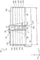
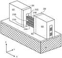
图1A是根据实施例的Ⅲ族-N晶体管的等距图;1A is an isometric view of a Group III-N transistor according to an embodiment;
图1B是图1A中所示的Ⅲ族-N晶体管的沟道区的截面图;1B is a cross-sectional view of a channel region of the III-N transistor shown in FIG. 1A;
图1C是根据实施例的Ⅲ族-N晶体管的等距图;1C is an isometric view of a Group III-N transistor according to an embodiment;
图2A是根据实施例的用于Ⅲ族-N晶体管的GaN晶体取向的等距图;2A is an isometric view of a GaN crystal orientation for a Group III-N transistor, according to an embodiment;
图2B是采用非平面GaN体的Ⅲ族-N晶体管的沟道区的截面图,其中非平面GaN主体具有图2A中所示的晶体取向;2B is a cross-sectional view of a channel region of a Group III-N transistor employing a non-planar GaN body having the crystallographic orientation shown in FIG. 2A;
图2C是图2B中所示的沟道区的能带图;Figure 2C is an energy band diagram of the channel region shown in Figure 2B;
图2D是根据实施例的用于Ⅲ族-N晶体管的GaN晶体取向的等距图;2D is an isometric view of a GaN crystal orientation for a Group III-N transistor, according to an embodiment;
图2E是采用非平面GaN主体的Ⅲ族-N晶体管的沟道区的截面图,其中非平面GaN主体具有图2D中所示的晶体取向;2E is a cross-sectional view of a channel region of a III-N transistor employing a non-planar GaN body having the crystallographic orientation shown in FIG. 2D;
图3是示出根据实施例的制造非平面高电压晶体管的方法的流程图;3 is a flowchart illustrating a method of fabricating a non-planar high voltage transistor according to an embodiment;
图4A、4B、4C、4D和4E是根据图3中所示的方法的实施例所制造的非平面高电压晶体管的等距图;以及Figures 4A, 4B, 4C, 4D and 4E are isometric views of non-planar high voltage transistors fabricated according to embodiments of the method shown in Figure 3; and
图5是根据本发明实施例的移动计算平台的SoC实施方式的功能框图。5 is a functional block diagram of an SoC implementation of a mobile computing platform according to an embodiment of the present invention.
具体实施方式Detailed ways
在下文的说明中,阐释了大量的细节,然而对于本领域技术人员来说显而易见的是,本发明可以在没有这些具体细节的情况下实现。在一些实例中,以框图的形式、而不是以细节的方式示出公知的方法和器件,以避免使本发明难以理解。整个说明书中提及的“实施例”表示结合实施例描述的特定特征、结构、功能或特性包含在本发明的至少一个实施例中。因此,在整个说明书中术语“在实施例中”在各种地方的出现不必指代本发明的相同实施例。此外,特定特征、结构、功能或特性可以以任何适合的方式组合在一个或多个实施例中。例如,第一实施例可以与第二实施例结合,只要这两个实施例不互相排斥。In the following description, numerous details are set forth, however, it will be apparent to those skilled in the art that the present invention may be practiced without these specific details. In some instances, well-known methods and devices are shown in block diagram form, rather than in detail, in order to avoid obscuring the present invention. Reference throughout this specification to an "embodiment" means that a particular feature, structure, function, or characteristic described in connection with the embodiment is included in at least one embodiment of the present invention. Thus, the appearances of the term "in an embodiment" in various places throughout the specification are not necessarily referring to the same embodiment of the invention. Furthermore, the particular features, structures, functions, or characteristics may be combined in any suitable manner in one or more embodiments. For example, the first embodiment may be combined with the second embodiment as long as the two embodiments are not mutually exclusive.
在本文中,术语“耦合”和“连接”以及它们的衍生物可以用于描述部件之间的结构关系。应该理解的是,这些术语不是要作为彼此的同义词。相反,在特定实施例中,“连接”可以用于表示两个或多个元件彼此直接物理或电接触。“耦合”可以用于表示两个或多个元件彼此直接或非直接(在它们之间具有其它中间元件)的物理或电接触,和/或两个或多个元件彼此合作或互动(例如,作为造成影响的关系)。As used herein, the terms "coupled" and "connected" and their derivatives may be used to describe structural relationships between components. It should be understood that these terms are not intended as synonyms for each other. Rather, in certain embodiments, "connected" may be used to mean that two or more elements are in direct physical or electrical contact with each other. "Coupled" may be used to mean that two or more elements are in direct or indirect physical or electrical contact with each other (with other intervening elements therebetween), and/or two or more elements cooperate or interact with each other (eg, as an influencing relationship).
在本文中使用的术语“在……之上”、“在……之下”、“在……之间”和“在……上”指的是一个材料层相对于另一层的相对位置。同样,例如,设置在另一层之上或之下的一层可以直接与另一层接触,或可以具有一个或多个中间层。此外,设置在两层之间的一层可以直接与这两层接触,或可以具有一个或多个中间层。相比之下,在第二层“上”的第一层与第二层直接接触。The terms "on", "under", "between" and "on" as used herein refer to the relative position of one layer of material with respect to another layer . Also, for example, a layer disposed above or below another layer may be in direct contact with another layer, or may have one or more intervening layers. Furthermore, a layer disposed between the two layers may be in direct contact with the two layers, or may have one or more intervening layers. In contrast, the first layer "on" the second layer is in direct contact with the second layer.
在本文中描述的是Ⅲ族氮化物(Ⅲ-N)半导体纳米线、以及用于制造高电压、高带宽场效应晶体管的制造技术的实施例。在特定实施例中,在集成高功率无线数据传输和/或具有低功率CMOS逻辑数据处理的高电压功率管理功能的SoC架构中采用这种晶体管。纳米线结构需要用于短沟道效应极好的静电控制的“环绕式栅极”,并且因此,容许将Ⅲ族-N晶体管超缩放至低于100nm的尺度。适合于宽带无线数据传输应用的高频操作是可能的,而大带隙Ⅲ-N材料的使用还提供高BV,从而可以产生用于无线数据传输应用的足够的RF输出功率。高Ft和高电压容量的这种组合还使本文中所描述的晶体管的使用成为可能,这是因为DC到DC转换器中的高速切换应用使用减小尺寸的电感元件。由于功率放大和DC到DC切换应用均是智能手机、平板电脑和其它移动平台中的关键功能块,所以针对这样的设备,本文描述的结构可以用于SoC解决方案中。Described herein are examples of Group III nitride (III-N) semiconductor nanowires, and fabrication techniques for fabricating high voltage, high bandwidth field effect transistors. In certain embodiments, such transistors are employed in SoC architectures that integrate high power wireless data transmission and/or high voltage power management functions with low power CMOS logic data processing. The nanowire structure requires a "wrap-around gate" for excellent electrostatic control of short-channel effects, and thus, allows for the over-scaling of III-N transistors to scales below 100 nm. High frequency operation suitable for broadband wireless data transmission applications is possible, while the use of large bandgap III-N materials also provides high BV, which can result in sufficient RF output power for wireless data transmission applications. This combination of highFt and high voltage capacity also enables the use of the transistors described herein because high speed switching applications in DC to DC converters use reduced size inductive components. Since both power amplification and DC-to-DC switching applications are key functional blocks in smartphones, tablets, and other mobile platforms, the architecture described herein can be used in SoC solutions for such devices.
在实施例中,利用可以包括多种Ⅲ族-N材料的多层半导体结构来形成纳米线、多个垂直叠置的纳米线,并且可以进一步用于将具有不同带隙的半导体材料合并到晶体管的各个区中(例如,可以将更宽带隙的材料合并在器件沟道与漏极触点之间的非本征漏极区中)。在示例性实施例中,栅极结构环绕沟道区的所有边,以提供用于缩放栅极长度(Lg)的沟道电荷的全选通限制。根据实施例,纳米线的一个或多个表面覆盖有宽带隙Ⅲ族-N材料,以提供以下中的一个或多个:增强的沟道迁移率、自发和压电极化的表层电荷[二维电子气(2DEG)]、界面状态的钝化、以及用于沟道电荷载流子限制的能量势垒。In an embodiment, nanowires, a plurality of vertically stacked nanowires are formed using multilayer semiconductor structures that may include multiple III-N materials, and may further be used to incorporate semiconductor materials with different band gaps into transistors (eg, higher bandgap material may be incorporated in the extrinsic drain region between the device channel and the drain contact). In an exemplary embodiment, the gate structure surrounds all sides of the channel region to provide full gate confinement of channel charge for scaling the gate length (Lg). According to an embodiment, one or more surfaces of the nanowire are covered with a wide bandgap Group III-N material to provide one or more of the following: enhanced channel mobility, spontaneous and piezoelectrically polarized surface charge [two dimensional electron gas (2DEG)], passivation of interface states, and energy barriers for channel charge carrier confinement.
图1A是根据实施例的Ⅲ族-N晶体管100的等距图。通常,Ⅲ族-N晶体管100是通常被称为高电子迁移率晶体管(HEMT)的栅极电压控制的器件(即,FET)。Ⅲ族-N晶体管100包括至少一个非平面结晶半导体主体,其位于与衬底层205的顶表面平行的平面上,晶体管100设置于衬底层205的顶表面上。在实施例中,衬底层205是绝缘的、或半绝缘的、和/或具有设置于其上的绝缘或半绝缘层,其上设置纳米线210A。在一个这样的实施例中,衬底层205是生长在支撑衬底上或转移到施主衬底上(未示出支撑衬底和施主衬底)的Ⅲ族-N半导体的顶层(图1A中所示)。在特定实施例中,衬底层205包括硅支撑衬底,Ⅲ族-N层外延生长在所述硅支撑衬底上,然而,所述支撑衬底还可以具有可选的材料(其可以或可以不与硅组合),包括但不限于锗、锑化铟、碲化铅、砷化铟、磷化铟、砷化镓、或锑化镓、碳(SiC)和蓝宝石。在另一个实施例中,其上设置晶体管100的衬底层205是介电层,从而衬底层205是掩埋氧化层(BoX),其可以例如通过将形成纳米线210A的一个或多个半导体层转移到衬底层205上来形成。FIG. 1A is an isometric view of a Group III-
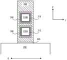
如图1A进一步示出的,Ⅲ族-N晶体管100的纵向长度L划分为源极区220、沟道区145、漏极区230和设置于它们之间的非本征漏极区235A。必须特别强调非本征漏极区235A,因为其对器件的BV具有显著影响。至少在沟道区245内,非平面结晶半导体主体通过除了形成主体的结晶半导体或形成衬底层205的材料以外的中间材料与衬底层205物理分隔开,以形成横向取向的纳米线210A。对于本文描述的实施例,纳米线210A的横截面几何结构可以从圆形到矩形有相当大的变化,从而纳米线210A的厚度(即,在z维度上)可以近似等于纳米线210A的宽度(即,在y维度上),或纳米线210A的厚度和宽度彼此可以有很大的不同(即,物理上类似于带状物,等等),以形成圆柱形和平行六面体的半导体主体。对于示例性实施例,纳米线210A的宽度在5和50纳米(nm)之间,但是这可以取决于实施方式而变化。As further shown in FIG. 1A, the longitudinal length L of the III-
在沟道区245内,纳米线210A具有比多晶材料大得多的长程有序(long rangeorder)。在示例性实施例中,沟道区245基本上是单晶,并且尽管此处被称为“单晶”,普通技术人员将意识到,低水平的晶体缺陷仍然可能作为不完美外延生长过程的工件而出现。在沟道区245内,纳米线210A是包括一种或多种Ⅲ族元素和氮(即,Ⅲ族-N半导体)的第一半导体材料的晶体排列。通常,沟道区245中的该第一Ⅲ族氮化物材料应该具有相对高的载流子迁移率,并且因此在实施例中,为了最小的杂质散射,沟道区245是基本上未掺杂的Ⅲ族氮化物材料(即,杂质浓度最小化)。在第一示例性实施例中,沟道区245是GaN。在第二示例性实施例中,沟道区245是氮化铟(InN)。因为InN具有比GaN大的载流子迁移率(与1900cm2/Vs相比的2700cm2/Vs),晶体管的度量(例如比导通电阻(Ron))可能对于InN实施例来说相对较好。在第三示例性实施例中,沟道区245是GaN的三元合金,例如铝镓氮化物(AlxGa1-xN),其中x小于1。在第四示例性实施例中,沟道区245是InN的三元合金,例如铝铟氮化物(AlxIn1-xN),其中x小于1。在其它实施例中,沟道区245是四元合金,其包括至少一种Ⅲ族元素和氮,例如InxAlyGa1-x-yN。Within the
至少在沟道区245内,纳米线210A被覆盖有第二半导体层215,其设置于纳米线210A的侧壁、顶部、和/或底表面中的一个或多个之上。在示例性实施例中,半导体层215直接设置于纳米线210A的至少两个相对的表面处。图1B是沿着穿过Ⅲ族-N晶体管200的沟道区245的B平面的截面图,其示出设置于纳米线210A(和纳米线210B)的全周长表面上的半导体215。如图2A中进一步示出的,半导体层215在非本征漏极区235A内也覆盖纳米线210A,其中层215用作电荷诱导层。At least within
半导体层215具有第二半导体成分,其带隙宽于沟道区245内的纳米线210A中使用的Ⅲ族-N材料的带隙。优选地,结晶半导体层215基本上是单晶(即,具有小于临界厚度的厚度),晶格与沟道区245内的纳米线210A中使用的Ⅲ族-N材料匹配。在示例性实施例中,半导体层215具有结晶度与纳米线210的结晶度相同的第二Ⅲ族-N材料,以在沟道区245内形成量子阱异质界面。The
通常,用于纳米线210A的所描述的任何Ⅲ族-N材料均可以用于半导体层215,这取决于纳米线210A所选择的材料,以便提供带隙比纳米线210A的带隙大的半导体层215。在纳米线210A是GaN的第一示例性实施例中,半导体层215是AlN。在纳米线210A是InN的第二示例性实施例中,半导体层215是GaN。在纳米线210A是AlxIn1-xN的第三示例性实施例中,半导体层215是AlyIn1-yN,其中y大于x。在纳米线210A是AlxGa1-xN的第四示例性实施例中,半导体层215是AlyGa1-yN,其中y大于x。包括至少一种Ⅲ族元素和氮的四元合金,例如Al1-x-yInxGayN(x、y<1)也是可能的。半导体层215还可以包括这些Ⅲ族氮化物的任何多层叠置,例如,AlxIn1-xN/AIN叠置有邻近(例如,GaN)纳米线210A的叠置的AIN层。In general, any of the Group III-N materials described for
即使在纳米线210A的所有表面上(顶部、底部和侧壁)出现半导体层215的情况下,如图1B中所描述的,厚度仍可以变化。半导体层215在沟道区245内用于至少两种功能。这两种功能是由于半导体结晶体210A内的极性键所引起的不对称和源于相对于半导体层215的这些键的极化方向。根据纳米线210A的晶体取向,纳米线210A的各种相对的表面与不同晶体平面对齐,从而使由半导体层215在这些相对的表面上导致的电场的影响发生变化。Even where the
在图2A所示的一个实施例中,纳米线210A的Ⅲ族氮化物所具有的晶体结构被称为纤锌矿结构。可以利用纤锌矿结构来形成本文所描述的GaN和其它Ⅲ族氮化物,所述纤锌矿结构因为其是非中心对称而著名,非中心对称意味着晶体缺少反对称性,并且更具体地,{0001}平面不相等。对于示例性GaN实施例,{0001}平面中的一个通常称为Ga-面(+c极性),并且另一个被称为N-面(-c极性)。通常对于平面Ⅲ族-N器件,{0001}平面中的一个或另一个更紧邻衬底表面,并且因此如果Ga(或其它Ⅲ族元素)的三个键指向衬底则可以被称为Ga极性(+c),或者如果Ga(或其它Ⅲ族元素)的三个键指向远离衬底的方向则可以被称为N极性(-c)。然而对于Ⅲ族-N晶体管200的第一实施例,纤锌矿晶体取向是使得具有晶格常数c的(1010)平面形成晶体的顶表面并且连接衬底层205。In one embodiment shown in FIG. 2A , the crystal structure of the group III nitride of the
如图2B中所进一步示出的,其中纳米线210A具有如图2A中取向的Ⅲ族氮化物材料,半导体层215包括在一个侧壁(例如,215B)上用作电荷诱导层的侧壁部分215A和215B,从而可以在邻近半导体层215的纳米线210A中形成2DEG 211A。如此取向,半导体层侧壁部分215A还可以用作背面势垒,以在沟道区245内限制电荷载流子。如图所示,第一侧壁部分215A基本上沿着

如图2B所进一步示出的,由于半导体层215的结晶,自发极化场PSP也出现在半导体层215内,并且与纳米线210A的自发极化场对齐。此外,当半导体层215处于与侧壁部分215A和215B的高度维度平行的方向(沿着如图2B所示的z维度)上的拉伸应变下时,压电极化场PPE在从第二侧壁部分215B到第一侧壁部分215A的方向上也与PSP对齐。因此,纳米线210A和半导体层215的极化在沿着紧邻第二侧壁部分215B的(0001)平面的异质界面处形成极化场。如麦克斯韦方程所描述的,极化场引起2DEG211A。As further shown in Figure 2B, due to the crystallization of the
对于Ⅲ族-N晶体管200的第二个实施例,纤锌矿晶体取向使得具有晶格常数a的(0001)平面形成晶体的顶表面并且连接衬底层205,如图2D所示。对于该实施例,如图4E所进一步示出的,出现在纳米线210A的顶部和底部上(215D和215C)的半导体层215分别用作电荷诱导层和背面势垒。于是纳米线210A内的半导体层215自发极化场PSP从顶表面部分215D被导向底表面部分215C。同样,非平面Ⅲ族-N晶体管200的极化穿过纳米线210A的厚度方向(沿着z维度的垂直方向)。因此,如图2E所示,纳米线210A以及半导体层部分215D和215C的极化分别在沿着(0001)平面和
在任一个晶体取向(图2A或图2D)中,背面势垒和电荷诱导层均由栅极叠置体250选通。图2C是根据纳米线210A(和纳米线210B)是GaN并且半导体层215是AlN的示例性实施例的非平面Ⅲ族氮化物晶体管的能带图,该非平面Ⅲ族氮化物晶体管由图2B所示的非平面结晶半导体主体形成,其中环绕的栅极结构如图1A中所示。如图2C所示,在零栅极偏压处,能带在纳米线210A的整个截面宽度上并且在半导体层部分215A和半导体层部分215B之间是非对称的。在纳米线210A内的能带由于极化场而弯曲在费米(Fermi)能级EF以下的位置处,出现电荷载流子。如能带图所示,图1B中所示的对称的栅极结构具有由纳米线210A的极化引起的非对称功能。因此,紧邻半导体层部分215B的栅极导体250调制沟道区内的2DEG111的电荷载流子密度,而紧邻半导体层部分215A的栅极导体250调制背面势垒。对于图2D中的取向,在栅极导体填充在纳米线210A与衬底层205之间以完全同轴地环绕纳米线210A的地方,提供相同的选通的背面势垒,如图1A中由沟道区245内的虚线所示。因此图2C的能带图还可以用于图2D的晶体取向。In either crystal orientation ( FIG. 2A or FIG. 2D ), both the backside barrier and the charge-inducing layer are gated by
如图1B中所进一步示出的,栅极叠置体包括栅极导体250,其通过设置于栅极导体下的栅极介电材料240与纳米线210A电隔离,以减少栅极导体与纳米线210A之间的泄露电流。由于栅极叠置体250A设置于半导体层215之上,所以可以将半导体层215和栅极叠置体215的栅极介电材料看作是复合介电叠置体。在图1B中示出的实施例中,还将栅极介电材料240设置于衬底层205与栅极导体250之间。如图1A中所示,同轴缠绕需要设置在纳米线210A与衬底层205之间的区域250A内的栅极导体。As further shown in FIG. 1B , the gate stack includes a
通常,栅极介电材料240可以包括本领域公知的适合于FET栅极电介质的任何材料中的一种或多种,并且优选为高K电介质(即,介电常数比大于氮化硅(Si3N4)的介电常数),例如,但不限于诸如氧化钆(Gd2O3)、氧化铪(HfO2)的高K氧化物;诸如HfSiO、TaSiO、AlSiO的高K硅酸盐;以及诸如HfON的高K氮化物。类似地,栅极导体250可以是本领域中公知的适合于晶体管栅极电极的任何材料。在实施例中,栅极导体250包括功函数金属,可以选择该功函数金属来获取期望的阈值电压(Vt)(例如,大于0V,等等)。示例性导电栅极材料包括钨(W)、铝(Al)、钛(Ti)、钽(Ta)、镍(Ni)、钼(Mo)、锗(Ge)、铂(Pt)、金(Au)、钌(Ru)、钯(Pd)、铱(Ir)、它们的合金和硅化物、碳化物、氮化物、磷化物、及其碳氮化物。In general,
回到图1A,纳米线210A还包括源极区220和漏极区230。在示例性实施例中,在源极区220和漏极区230内,纳米线210A是在沟道区245中出现的相同的Ⅲ族氮化物半导体材料,但是还包括更高的掺杂浓度,例如n型杂质(即,N+)。在特定实施例中,源极区220和漏极区230内的纳米线210A与沟道区245内的纳米线210A保持相同的单晶。在第一实施例中,半导体材料层212A与源极区220和/或漏极区230内的纳米线210接触。对于Ⅲ族氮化物晶体管200,纳米线210A夹在半导体材料层212A与212B之间。在示例性实施例中,在半导体材料层212A有助于纳米线210A在沟道区245内的底切的地方,半导体材料层212A与纳米线210A具有不同的材料。Returning to FIG. 1A , the
在实施例中,半导体材料层212A是针对纳米线210A的实施例所描述的不同于纳米线210A所使用的任何Ⅲ族氮化物。例如,半导体材料层212A可以是AlN、GaN、InN、AlzIn1-zN或AlzGa1-zN,其中z不同于x。在一个实施例中,半导体材料层212A的带隙低于纳米线210A的带隙(例如,z小于x,其中纳米线210A和半导体材料层212A均是三元的),以帮助减小源极/漏极接触电阻。在可选的实施例中,半导体材料层212A的带隙高于纳米线210A的带隙(例如,z大于x,其中纳米线210A和半导体材料层212A均是三元的)。在纳米线210A的Ⅲ族氮化物和半导体材料层212A的Ⅲ族氮化物是合金或混合的情况下,可以将非本征漏极区235A内的带隙有利地增加到沟道区245中的带隙与半导体材料层212A中的带隙的中间,从而实现甚至更高的BV。同样,根据实施例,晶体管100可以将牺牲性的半导体并入沟道区245内,以选择性地减少或增加沟道区245中采用的半导体材料的带隙。In an embodiment, the layer of
图1C是根据实施例的Ⅲ族-N晶体管200的等距图。尽管Ⅲ族-N晶体管100具有非本征漏极区235A,其近似等于源极触点222A与沟道区245之间的间距(即,由电介质垫片255确定),但是Ⅲ族-N晶体管200具有非本征漏极区235B,其大于源极触点222B与沟道区245之间的间距。非本征漏极区235A、235B可以是轻掺杂的并且还包括半导体层215,如图1A和1C中所示。在非本征漏极区235A、B内,半导体层215用作电荷诱导层并且由于非本征漏极区的纵向长度是BV所期望的函数,因此Ⅲ族-N晶体管200具有比Ⅲ族-N晶体管100大的BV。FIG. 1C is an isometric view of a Group III-
在一个示例性实施例中,非本征漏极区235B是第一和第二半导体材料的合金,以提供介于第一和第二半导体材料的带隙之间的带隙。如图1C中的空心箭头所示出的,在非本征漏极区235B内,第一和第二半导体材料的合金是无序的多层结构的形式。该多层结构包括夹在半导体材料层212A与212B之间的纳米线210A的Ⅲ族氮化物材料,其通过非本征漏极区235B延伸并且将沟道区245耦合到漏极区230。利用与半导体材料层212A和212B相邻的纳米线210A的相对的边,可以在非本征漏极区235B的部分内实现好的合金均匀性。In one exemplary embodiment, the
在实施例中,Ⅲ族氮化物晶体管包括嵌有源极和/或漏极触点的纳米线的源极区和/或漏极区。图1C示出源极触点222B,其完全同轴地环绕纳米线210A以填充在纳米线210A与衬底层205之间的间隙中。如图1A所示,源极触点222A并未完全环绕纳米线210A,这是因为半导体层212A和212B的存在。源极触点222A、222B可以包括欧姆性金属化层,并且还可以包括与纳米线210A不同成分的外延生长半导体。例如,源极触点222A、222B可以包括隧道结(例如,在源极区220内环绕纳米线210A的p+层)。可以利用这种隧道结来提供超陡峭的导通和截止(即,改进的亚阈值性能),以减少断开状态泄露电流。In an embodiment, the III-nitride transistor includes source and/or drain regions of nanowires embedded with source and/or drain contacts. FIG. 1C shows a
纳米线210A还包括漏极区230。类似于源极区,漏极区可以或多或少地嵌有漏极触点232。在图1C中,在漏极区230内漏极触点232B完全同轴地环绕纳米线210A,以填充在纳米线210A与衬底层205之间的间隙中。如图1A所示,漏极触点232A并未完全环绕纳米线210A,这是由于半导体层212A和212B的存在。类似于源极触点222A、222B,漏极触点232A、232B可以包括欧姆性金属化层,并且还可以包括与纳米线210A不同成分的外延生长半导体。
在实施例中,如图1A和1C中所示,Ⅲ族-N晶体管包括纳米线的垂直叠置体,以针对衬底层上的给定的占用空间来实现较大的电流携载能力(例如,较大的驱动电流)。可以将任何数量的纳米线垂直叠置,这取决于制造限制,并且每个纳米线的纵轴基本上平行于衬底层205的顶表面。在图1A或1C中所示出的示例性实施例中,纳米线210A、210B的每一个在沟道区245内具有相同的第一半导体材料。在其它实施例中,纳米线210A、210B的每一个由栅极叠置体250A(例如,如图1B、2B和2E中所进一步示出的)同轴环绕。至少栅极介电层240将被设置于纳米线210A与210B之间,但是在图1B所示的示例性实施例中,栅极导体也出现在纳米线210A、210B的每一个的沟道区之间。In embodiments, as shown in FIGS. 1A and 1C, III-N transistors include vertical stacks of nanowires to achieve greater current-carrying capabilities for a given footprint on the substrate layer (eg, , larger drive current). Any number of nanowires can be stacked vertically, depending on manufacturing constraints, and the longitudinal axis of each nanowire is substantially parallel to the top surface of
在图1C所示的实施例中,多个纳米线210B中的每一个通过非本征漏极区235B中的半导体材料物理耦合在一起。对于包括多个纳米线210A、210B的实施例,Ⅲ族-N晶体管100、200具有多个漏极区,在纳米线的垂直叠置体内的每个纳米线对应一个漏极区。可以利用漏极触点(例如,232B)同轴地环绕每个漏极区,该漏极触点完全同轴地环绕漏极区中的每一个,从而填充在纳米线210A、210B之间的间隙中。类似地,源极触点222B可以完全同轴地环绕多个源极区。In the embodiment shown in FIG. 1C, each of the plurality of
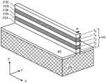
现在提供针对晶体管200和201中的每一个的制造过程的显著部分的简要描述。图3是示出根据实施例的制造非平面高电压晶体管200和201的方法300的流程图。尽管方法300突出了主要操作,但是每个操作可能需要更多的过程顺序,并且图3中的操作的标号或操作的相对位置并不暗示任何顺序。图4A、4B、4C、4D和4E是根据方法300的实施例制造的非平面Ⅲ族-N晶体管100、200的等距图。A brief description of salient portions of the fabrication process for each of
在操作301处,利用任何标准化学气相沉积(CVD)、分子束外延(MBE)、氢化物气相外延(HVPE)生长技术等(利用标准前驱体、温度,等)来生长单晶半导体材料的叠置体。生长至少两种不同的半导体层来作为外延叠置体的一部分。在实施例中,层212A、212B和212C是第一Ⅲ族氮化物材料,其中第二Ⅲ族氮化物设置在它们之间。At
在操作305处,通过针对作为外延叠置体的部分而生长的特定材料,利用本领域公知的任何等离子或湿式化学蚀刻技术,对外延叠置体进行蚀刻来界定纳米线(例如,长和宽)。如图4A中所示,在操作303处,将鳍结构410蚀刻到外延叠置体中以形成纳米线210A、210B,其可以与半导体层212A、212B和212C交替。如图所示,纳米线210A和210B中的每一个均设置于半导体层212A、212B之上和之下。层的厚度T1—T4取决于所期望的纳米线尺寸,并且还取决于在纳米线210A和210B上形成半导体层215之后,利用栅极叠置体回填厚度T1、T3的能力。图4A中还示出,在衬底层205之上的鳍结构401的任一侧上,例如通过浅沟槽隔离技术来形成绝缘层407。At
回到图3,在操作305处,形成漏极触点以部分地(如图1A中)或完全地(如图1C中)环绕纳米线210A和210B。在操作310处,以类似的方法形成源极触点。在操作315处,栅极导体完全同轴地环绕纳米线210A和210B的纵向沟道长度。于是在操作320处例如使用常规的互连技术完成器件。Returning to Figure 3, at
图4B示出需要形成设置于鳍结构410上的牺牲栅极412的操作305、310和315的一个实施例。在一个这样的实施例中,牺牲栅极412由牺牲栅极氧化层和牺牲多晶硅栅极层组成,将所述牺牲栅极氧化层和牺牲多晶硅栅极层均厚沉积并利用常规的光刻和等离子蚀刻技术来图案化。在牺牲栅极412的侧壁上形成垫片,并且可形成夹层介电层来覆盖牺牲栅极412。可对夹层介电层进行抛光来暴露用于替换栅极、或后栅极、过程的牺牲栅极412。参考图4C,已经去除牺牲栅极412,留下垫片255和夹层介电层(ILD)420、421的部分。如图4C中所进一步示出的,在最初由牺牲栅极412覆盖的沟道区中去除半导体层212A、212B和212C。于是留下第一半导体材料的分立的纳米线210A和210B。FIG. 4B illustrates one embodiment of
如图4D中所示,然后在沟道区245内形成同轴环绕纳米线210A、210B的栅极叠置体250A。图4D示出在半导体层215的外延生长、栅极电介质240的沉积以及栅极导体250的沉积以回填由选择性蚀刻半导体层212A、212B和212C所形成的间隙的栅极叠置体。也就是说,将外延叠置体蚀刻成分立的Ⅲ族-N纳米线之后,在夹层介电层420、421之间的沟槽中形成栅极叠置体。此外,图4D示出了在栅极叠置体250A形成之后,去除夹层介电层420后的结果。对于包括非本征漏极区235B(例如,Ⅲ族氮化物晶体管200)的实施例,在非本征漏极区235A内保留一部分夹层介电层421(例如,利用夹层电介质的光刻界定的掩蔽蚀刻)。对于可选的实施例(例如,对于晶体管Ⅲ族氮化物晶体管100),不保留ILD 421的部分。As shown in FIG. 4D , a
对于包括完全同轴地环绕纳米线210A、210B的源极触点和漏极触点的实施例,一旦去除ILD层420、421,那么没有被栅极叠置体保护的半导体层212A和212B的部分则相对于第一半导体材料的纳米线210A、210B被选择性地去除,以在纳米线210A、210B与衬底层205之间形成间隙。于是第一半导体的分立部分保留在源极区220和漏极区230中,如图4D中所示的。然后可以通过回填形成在源极区220和漏极区230内的间隙来形成源极触点222和漏极触点232(如图2A中所示)。在一个这样的实施例中,通过CVD、原子层沉积(ALD)或金属回流来统一沉积触点金属。在可选的实施例中,在半导体层212A和212B以及源极区和漏极区内的纳米线210A和210B的侧壁上形成源极触点222A和漏极触点232A。然后在操作320处例如利用常规的互连金属化等来准备完成器件。For embodiments that include source and drain contacts that completely
在图4E所示的其它实施例中,可以将ILD421的任何保留的部分选择性地迁移到垫片255、栅极导体250和源极触点222B、漏极触点232B。然后可以在纳米线210A、210B和半导体层212A、212B、212C中的一个之上选择性地去除纳米线210A、210B和半导体层212A、212B、212C中的另一个。在示例性实施例中,然后在(多个)底切间隙中重新外延生长具有比纳米线210A、210B大的带隙的结晶半导体材料。然后半导体层212A、212B、212C可以用作非本征漏极区235B内的电荷诱导层。可以在纳米线210A、210B的侧壁上(例如,在晶体取向是如图2B中所示的情况下)另外生长半导体层215。可替换地,或此外,在去除ILD 421的剩余部分之后,可以将诸如Al、Ga或Zn之类的扩散元素并入到非本征漏极区235B内的第一半导体上。In other embodiments shown in FIG. 4E, any remaining portion of
在实施例中,在非本征漏极区235B内出现的半导体材料通过热退火熔合。例如,可以混合第一半导体材料210A、210B和半导体层212A、212B和212C(即,无序的多层结构)。可替换地,热退火可以将半导体材料与扩散元素(例如,Al、Ga或Zn)混合。在一个这样的实施例中,热退火与源极触点和漏极触点的形成(例如,操作305和310)同时进行。值得注意的是,可以在源极触点222和漏极触点232形成之后、和/或在非本征漏极区235B退火之后进行牺牲栅极412的替换。同样,可以在非本征漏极区235B的热退火之后生长半导体层215,以保持沟道区245和/或非本征漏极区235B内的半导体层215与纳米线210A、210B之间的不连贯的异质界面。In an embodiment, the semiconductor material present within the
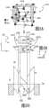
图5是根据本发明的实施例的移动计算平台的SoC实施方式的功能性框图。移动计算平台700可以是被配置为电子数据显示、电子数据处理、以及无线电子数据传输中的每一个的任何便携式设备。例如,移动计算平台700可以是平板电脑、智能手机、膝上型计算机等中的任何一个,并且包括在示例性实施例中是允许接收用户输入的触摸屏(例如,电容性、电感性、电阻性,等)的显示屏705、SoC 710、以及电池713。如所示,SoC710的集成水平越高,在移动计算平台700内的形状因素就可以越多地被电池713占据以用于在充电之间最长的运转寿命,或越多地被诸如固态硬盘的存储器(未描述)占据以用于最大的功能。5 is a functional block diagram of an SoC implementation of a mobile computing platform in accordance with an embodiment of the present invention.
根据其应用,移动计算平台700可以包括其它部件,其包括但不限于易失性存储器(例如,DRAM)、非易失性存储器(例如,ROM)、闪存存储器、图形处理器、数字信号处理器、密码处理器、芯片组、天线、显示器、触摸屏显示器、触摸屏控制器、电池、音频编解码器、视频编解码器、功率放大器、全球定位系统(GPS)设备、罗盘、加速计、陀螺仪、扬声器、相机、以及大容量存储设备(例如硬盘驱动器、光盘(CD)、数字通用光盘(DVD),等等)。Depending on its application,
在扩展视图720中进一步示出了SoC 710。根据实施例,SoC 710包括硅衬底500(即,芯片)的一部分,其上制造以下部件中的两个或多个:功率管理集成电路(PMIC)715、包括RF发送器和/或接收器的RF集成电路(RFIC)725、其控制器711,以及一个或多个中央处理器核730、731。如本领域技术人员将领会的,关于这些功能不同的电路模块,除了在PMIC715和RFIC 725中,通常采用专用的CMOS晶体管,该PMIC 715和RFIC 725通常分别使用LDMOS和Ⅲ-ⅤHBT技术。然而在本发明的实施例中,PMIC715和RFIC 725采用本文描述的Ⅲ族氮化物晶体管(例如,Ⅲ族氮化物晶体管100或200)。在其它实施例中,采用本文描述的Ⅲ族氮化物晶体管的PMIC 715和RFIC 725与一个或多个控制器711集成,并且在硅CMOS工艺中提供的处理器核720、730与PMIC 715和RFIC 725单片地集成到硅衬底500上。应该领会的是,在PMIC 715和/或RFIC 725内,本文描述的高电压、高频能力Ⅲ族氮化物晶体管不需要被用于将CMOS排除在外,而是相反还可以将硅CMOS包括在PMIC 715和RFIC 725中的每一个中。SoC 710 is further shown in expanded
RFIC 725可以实现多种无线标准或协议中的任何一种,包括但不限于Wi-Fi(IEEE802.11系列)、WiMAX(IEEE 802.16系列)、IEEE 802.20、长期演进(LTE)、Ev-DO、HSPA+、HSDPA+、HSUPA+、EDGE、GSM、GPRS、CDMA、TDMA、DECT、蓝牙、它们的衍生物、以及任何其它定名为3G、4G、5G及其以后的无线协议。平台725可以包括多个通信芯片。例如,第一个通信芯片可以专用于较短范围无线通信,例如Wi-Fi和蓝牙;并且第二个通信芯片可以专用于较长范围的无线通信,例如GPS、EDGE、GPRS、CDMA、WiMAX、LTE、Ev-DO、等等。The
本文描述的Ⅲ族氮化物晶体管可以特别用于出现高电压摆动的情况(例如,在PMIC 715内的7-10V电池功率调节、DC到DC转换,等等)。如所示出的,在示例性实施例中,PMIC 715具有耦合到电池713的输入端,并且具有向SoC 710中的所有其它功能模块提供电流源的输出端。在其它实施例中,在移动计算平台700内但在SoC 710外提供附加的IC的情况下,PMIC 715的输出端还向SoC 710外部的所有这些附加的IC提供电流源。如进一步示出的,在示例性实施例中,RFIC 715具有耦合到天线的输出端,并且还可以具有耦合到SoC710上的诸如RF模拟和数字基带模块(未示出)的通信模块的输入端。可替换地,可以从SoC710在片下IC上提供这种通信模块,并且将其耦合到SoC 710中用于传输。根据使用的Ⅲ族氮化物材料,本文描述的Ⅲ族氮化物晶体管(例如,200或201)还可以提供功率放大晶体管所需要的大的功率附加效率(PAE),该功率放大晶体管具有至少是载频的十倍大小的Ft(例如,在为3G或GSM蜂窝通信而设计的RFIC 725中是1.9GHz)。The III-nitride transistors described herein may be particularly useful in situations where high voltage swings occur (eg, 7-10V battery power regulation within the
应该理解的是,上述描述是示例性而非限制性的。例如,尽管附图中的流程图示出了由本发明的特定实施例所执行的操作的特定顺序,但是应该理解的是,可以不需要这种顺序(例如,可选的实施例可以采用不同的顺序来执行操作、组合特定操作、重叠特定操作,等等)。此外,对于本领域技术人员来说,一经阅读并理解了上述描述后,许多其它实施例将是显而易见的。尽管已经参考特定的示例性实施例描述了本发明,但是应该认识到,本发明并不限于所描述的实施例,而是可以在所附权利要求的精神和范围内,在做出修改和替换的情况下实现。因此,应该参考所附权利要求、以及为这些权利要求赋予权利的等价物的完整范围来确定本发明的范围。It should be understood that the foregoing description is exemplary and not restrictive. For example, although the flowcharts in the figures illustrate a particular order of operations performed by particular embodiments of the invention, it is to be understood that such order may not be required (eg, alternative embodiments may employ different perform operations sequentially, combine certain operations, overlap certain operations, etc.). Furthermore, many other embodiments will be apparent to those skilled in the art upon reading and understanding the foregoing description. Although the present invention has been described with reference to specific exemplary embodiments, it should be recognized that the invention is not limited to the described embodiments, but may be subject to modifications and substitutions within the spirit and scope of the appended claims realized under the circumstances. Therefore, the scope of the invention should be determined with reference to the appended claims, along with the full scope of equivalents to which such claims are entitled.
Claims (27)
Priority Applications (1)
| Application Number | Priority Date | Filing Date | Title |
|---|---|---|---|
| CN201710025642.0ACN106887453B (en) | 2011-12-19 | 2011-12-19 | Group III-N Nanowire Transistors |
Applications Claiming Priority (3)
| Application Number | Priority Date | Filing Date | Title |
|---|---|---|---|
| CN201180075624.4ACN104011868B (en) | 2011-12-19 | 2011-12-19 | group III-N nanowire transistors |
| PCT/US2011/065919WO2013095343A1 (en) | 2011-12-19 | 2011-12-19 | Group iii-n nanowire transistors |
| CN201710025642.0ACN106887453B (en) | 2011-12-19 | 2011-12-19 | Group III-N Nanowire Transistors |
Related Parent Applications (1)
| Application Number | Title | Priority Date | Filing Date |
|---|---|---|---|
| CN201180075624.4ADivisionCN104011868B (en) | 2011-12-19 | 2011-12-19 | group III-N nanowire transistors |
Publications (2)
| Publication Number | Publication Date |
|---|---|
| CN106887453A CN106887453A (en) | 2017-06-23 |
| CN106887453Btrue CN106887453B (en) | 2020-08-21 |
Family
ID=48669010
Family Applications (2)
| Application Number | Title | Priority Date | Filing Date |
|---|---|---|---|
| CN201710025642.0AActiveCN106887453B (en) | 2011-12-19 | 2011-12-19 | Group III-N Nanowire Transistors |
| CN201180075624.4AActiveCN104011868B (en) | 2011-12-19 | 2011-12-19 | group III-N nanowire transistors |
Family Applications After (1)
| Application Number | Title | Priority Date | Filing Date |
|---|---|---|---|
| CN201180075624.4AActiveCN104011868B (en) | 2011-12-19 | 2011-12-19 | group III-N nanowire transistors |
Country Status (5)
| Country | Link |
|---|---|
| US (5) | US9240410B2 (en) |
| CN (2) | CN106887453B (en) |
| DE (1) | DE112011105945B4 (en) |
| TW (3) | TWI592992B (en) |
| WO (1) | WO2013095343A1 (en) |
Families Citing this family (68)
| Publication number | Priority date | Publication date | Assignee | Title |
|---|---|---|---|---|
| CN106887453B (en)* | 2011-12-19 | 2020-08-21 | 英特尔公司 | Group III-N Nanowire Transistors |
| US9245989B2 (en)* | 2011-12-19 | 2016-01-26 | Intel Corporation | High voltage field effect transistors |
| WO2013101004A1 (en)* | 2011-12-28 | 2013-07-04 | Intel Corporation | Contact techniques and configurations for reducing parasitic resistance in nanowire transistors |
| US8896101B2 (en)* | 2012-12-21 | 2014-11-25 | Intel Corporation | Nonplanar III-N transistors with compositionally graded semiconductor channels |
| WO2015047316A1 (en) | 2013-09-27 | 2015-04-02 | Intel Corporation | Composite high-k metal gate stack for enhancement mode gan semiconductor devices |
| EP3050111A4 (en)* | 2013-09-27 | 2017-06-07 | Intel Corporation | Improved cladding layer epitaxy via template engineering for heterogeneous integration on silicon |
| KR102138871B1 (en)* | 2013-09-27 | 2020-07-28 | 인텔 코포레이션 | Semiconductor device having group iii-v material active region and graded gate dielectric |
| US9455150B2 (en) | 2013-12-24 | 2016-09-27 | Intel Corporation | Conformal thin film deposition of electropositive metal alloy films |
| US9893167B2 (en) | 2014-03-24 | 2018-02-13 | Intel Corporation | Integration methods to fabricate internal spacers for nanowire devices |
| JP2015207651A (en)* | 2014-04-21 | 2015-11-19 | 日本電信電話株式会社 | Semiconductor device |
| US9543440B2 (en)* | 2014-06-20 | 2017-01-10 | International Business Machines Corporation | High density vertical nanowire stack for field effect transistor |
| US9269777B2 (en)* | 2014-07-23 | 2016-02-23 | Taiwan Semiconductor Manufacturing Company, Ltd. | Source/drain structures and methods of forming same |
| US9306019B2 (en)* | 2014-08-12 | 2016-04-05 | GlobalFoundries, Inc. | Integrated circuits with nanowires and methods of manufacturing the same |
| WO2016043748A1 (en) | 2014-09-18 | 2016-03-24 | Intel Corporation | Wurtzite heteroepitaxial structures with inclined sidewall facets for defect propagation control in silicon cmos-compatible semiconductor devices |
| US10229991B2 (en) | 2014-09-25 | 2019-03-12 | Intel Corporation | III-N epitaxial device structures on free standing silicon mesas |
| US10573647B2 (en) | 2014-11-18 | 2020-02-25 | Intel Corporation | CMOS circuits using n-channel and p-channel gallium nitride transistors |
| US10056456B2 (en) | 2014-12-18 | 2018-08-21 | Intel Corporation | N-channel gallium nitride transistors |
| EP3235009A4 (en)* | 2014-12-19 | 2018-07-25 | INTEL Corporation | Selective deposition utilizing sacrificial blocking layers for semiconductor devices |
| CN105990414A (en)* | 2015-02-06 | 2016-10-05 | 联华电子股份有限公司 | Semiconductor structure and manufacturing method thereof |
| CN104934479A (en)* | 2015-05-11 | 2015-09-23 | 中国科学院半导体研究所 | III-V clan nano wire planar transistor based on SOI substrate and preparation method thereof |
| WO2016186654A1 (en) | 2015-05-19 | 2016-11-24 | Intel Corporation | Semiconductor devices with raised doped crystalline structures |
| US10388777B2 (en) | 2015-06-26 | 2019-08-20 | Intel Corporation | Heteroepitaxial structures with high temperature stable substrate interface material |
| US9818872B2 (en) | 2015-06-30 | 2017-11-14 | Taiwan Semiconductor Manufacturing Company, Ltd. | Multi-gate device and method of fabrication thereof |
| US9853101B2 (en) | 2015-10-07 | 2017-12-26 | Taiwan Semiconductor Manufacturing Company, Ltd. | Strained nanowire CMOS device and method of forming |
| US9899387B2 (en)* | 2015-11-16 | 2018-02-20 | Taiwan Semiconductor Manufacturing Company, Ltd. | Multi-gate device and method of fabrication thereof |
| US10204985B2 (en)* | 2015-11-16 | 2019-02-12 | Taiwan Semiconductor Manufacturing Co., Ltd. | Structure and formation method of semiconductor device structure |
| WO2017096781A1 (en) | 2015-12-07 | 2017-06-15 | 中国科学院微电子研究所 | Nanowire semiconductor device provided with high quality epitaxial layer, and manufacturing method for nanowire semiconductor device |
| CN105633166B (en) | 2015-12-07 | 2019-06-18 | 中国科学院微电子研究所 | Nanowire semiconductor device with high-quality epitaxial layer and manufacturing method thereof |
| KR102434993B1 (en)* | 2015-12-09 | 2022-08-24 | 삼성전자주식회사 | Semiconductor device |
| US9425291B1 (en) | 2015-12-09 | 2016-08-23 | International Business Machines Corporation | Stacked nanosheets by aspect ratio trapping |
| US9548381B1 (en)* | 2015-12-14 | 2017-01-17 | Globalfoundries Inc. | Method and structure for III-V nanowire tunnel FETs |
| WO2017111869A1 (en) | 2015-12-24 | 2017-06-29 | Intel Corporation | Transition metal dichalcogenides (tmdcs) over iii-nitride heteroepitaxial layers |
| KR102413782B1 (en) | 2016-03-02 | 2022-06-28 | 삼성전자주식회사 | Semiconductor devices |
| US9570552B1 (en)* | 2016-03-22 | 2017-02-14 | Globalfoundries Inc. | Forming symmetrical stress liners for strained CMOS vertical nanowire field-effect transistors |
| US9882000B2 (en)* | 2016-05-24 | 2018-01-30 | Northrop Grumman Systems Corporation | Wrap around gate field effect transistor (WAGFET) |
| FR3051970B1 (en)* | 2016-05-25 | 2020-06-12 | Commissariat A L'energie Atomique Et Aux Energies Alternatives | REALIZATION OF A CHANNEL STRUCTURE FORMED OF A PLURALITY OF CONSTRAINED SEMICONDUCTOR BARS |
| CN105870062B (en)* | 2016-06-17 | 2019-05-31 | 中国科学院微电子研究所 | High quality nanowire CMOS device, method of manufacturing the same, and electronic apparatus including the same |
| US9620611B1 (en) | 2016-06-17 | 2017-04-11 | Acorn Technology, Inc. | MIS contact structure with metal oxide conductor |
| CN107546125B (en)* | 2016-06-24 | 2020-05-15 | 上海新昇半导体科技有限公司 | Nanowire-based high electron mobility transistor and manufacturing method thereof |
| US10134905B2 (en)* | 2016-06-30 | 2018-11-20 | International Business Machines Corporation | Semiconductor device including wrap around contact, and method of forming the semiconductor device |
| CN106549047B (en)* | 2016-11-03 | 2020-10-02 | 武汉华星光电技术有限公司 | Nanowire junction-free transistor and preparation method thereof |
| CN108063143B (en)* | 2016-11-09 | 2020-06-05 | 上海新昇半导体科技有限公司 | A kind of complementary transistor device structure and fabrication method thereof |
| WO2018094205A1 (en) | 2016-11-18 | 2018-05-24 | Acorn Technologies, Inc. | Nanowire transistor with source and drain induced by electrical contacts with negative schottky barrier height |
| US10170378B2 (en)* | 2016-11-29 | 2019-01-01 | Taiwan Semiconductor Manufacturing Co., Ltd. | Gate all-around semiconductor device and manufacturing method thereof |
| US10290546B2 (en) | 2016-11-29 | 2019-05-14 | Taiwan Semiconductor Manufacturing Co., Ltd. | Threshold voltage adjustment for a gate-all-around semiconductor structure |
| CN106847910B (en)* | 2017-03-09 | 2020-07-07 | 复旦大学 | A kind of GaN-based semiconductor device and preparation method thereof |
| US10535780B2 (en)* | 2017-05-08 | 2020-01-14 | Taiwan Semiconductor Manufacturing Co., Ltd. | Semiconductor device including an epitaxial layer wrapping around the nanowires |
| US11101270B2 (en)* | 2017-06-29 | 2021-08-24 | Intel Corporation | Techniques and mechanisms for operation of stacked transistors |
| WO2019066953A1 (en) | 2017-09-29 | 2019-04-04 | Intel Corporation | Group iii-nitride (iii-n) devices with reduced contact resistance and their methods of fabrication |
| US12125888B2 (en) | 2017-09-29 | 2024-10-22 | Intel Corporation | Group III-nitride (III-N) devices with reduced contact resistance and their methods of fabrication |
| US11335801B2 (en) | 2017-09-29 | 2022-05-17 | Intel Corporation | Group III-nitride (III-N) devices with reduced contact resistance and their methods of fabrication |
| US11557667B2 (en) | 2017-09-30 | 2023-01-17 | Intel Corporation | Group III-nitride devices with improved RF performance and their methods of fabrication |
| WO2019139619A1 (en)* | 2018-01-12 | 2019-07-18 | Intel Corporation | Source contact and channel interface to reduce body charging from band-to-band tunneling |
| CN108519174B (en)* | 2018-03-27 | 2020-09-08 | 中国电子科技集团公司第十三研究所 | GaN bridge type absolute pressure sensor and manufacturing method |
| US11257818B2 (en) | 2018-09-27 | 2022-02-22 | Taiwan Semiconductor Manufacturing Co., Ltd. | Fin-based field effect transistors |
| KR102254858B1 (en)* | 2018-09-27 | 2021-05-26 | 타이완 세미콘덕터 매뉴팩쳐링 컴퍼니 리미티드 | Fin-based field effect transistors |
| US11387329B2 (en)* | 2018-09-28 | 2022-07-12 | Intel Corporation | Tri-gate architecture multi-nanowire confined transistor |
| US11101360B2 (en)* | 2018-11-29 | 2021-08-24 | Taiwan Semiconductor Manufacturing Co., Ltd. | Method of manufacturing a semiconductor device and a semiconductor device |
| CN109616519A (en)* | 2018-12-06 | 2019-04-12 | 贵阳学院 | A zero subthreshold swing zero impact ionization transistor device and manufacturing method |
| US11355363B2 (en) | 2019-08-30 | 2022-06-07 | Taiwan Semiconductor Manufacturing Company, Ltd. | Semiconductor devices and methods of manufacturing |
| US11165032B2 (en)* | 2019-09-05 | 2021-11-02 | Taiwan Semiconductor Manufacturing Co., Ltd. | Field effect transistor using carbon nanotubes |
| EP4029139A4 (en) | 2019-09-13 | 2023-09-27 | Milwaukee Electric Tool Corporation | WIDE BAND GAP SEMICONDUCTOR POWER CONVERTERS |
| CN111243960A (en)* | 2020-01-20 | 2020-06-05 | 中国科学院上海微系统与信息技术研究所 | Preparation method of semiconductor nanowire and field effect transistor |
| US11855225B2 (en)* | 2020-02-27 | 2023-12-26 | Taiwan Semiconductor Manufacturing Co., Ltd. | Semiconductor device with epitaxial bridge feature and methods of forming the same |
| US11257917B2 (en)* | 2020-06-05 | 2022-02-22 | Qualcomm Incorporated | Gate-all-around (GAA) transistors with additional bottom channel for reduced parasitic capacitance and methods of fabrication |
| KR102858022B1 (en) | 2020-10-19 | 2025-09-12 | 삼성전자주식회사 | Semiconductor device |
| US20230095007A1 (en)* | 2021-09-24 | 2023-03-30 | Intel Corporation | Integrated circuit structures having metal-containing source or drain structures |
| US12362172B2 (en)* | 2022-01-10 | 2025-07-15 | Globalfoundries U.S. Inc. | Integration of compound-semiconductor-based devices and silicon-based devices |
Citations (1)
| Publication number | Priority date | Publication date | Assignee | Title |
|---|---|---|---|---|
| CN101273459A (en)* | 2005-06-16 | 2008-09-24 | 昆南诺股份有限公司 | semiconductor nanowire transistor |
Family Cites Families (55)
| Publication number | Priority date | Publication date | Assignee | Title |
|---|---|---|---|---|
| US6664575B2 (en) | 2000-12-05 | 2003-12-16 | Showa Denko Kabushiki Kaisha | GaInP stacked layer structure and field-effect transistor manufactured using the same |
| US7030428B2 (en) | 2001-12-03 | 2006-04-18 | Cree, Inc. | Strain balanced nitride heterojunction transistors |
| US7135728B2 (en) | 2002-09-30 | 2006-11-14 | Nanosys, Inc. | Large-area nanoenabled macroelectronic substrates and uses therefor |
| US6921700B2 (en)* | 2003-07-31 | 2005-07-26 | Freescale Semiconductor, Inc. | Method of forming a transistor having multiple channels |
| US7101761B2 (en)* | 2003-12-23 | 2006-09-05 | Intel Corporation | Method of fabricating semiconductor devices with replacement, coaxial gate structure |
| FR2875338B1 (en) | 2004-09-13 | 2007-01-05 | Picogiga Internat Soc Par Acti | METHOD FOR PRODUCING PIEZOELECTRIC HEMT STRUCTURES WITH NO ZERO ALLOYS |
| US20060086977A1 (en)* | 2004-10-25 | 2006-04-27 | Uday Shah | Nonplanar device with thinned lower body portion and method of fabrication |
| KR100594327B1 (en)* | 2005-03-24 | 2006-06-30 | 삼성전자주식회사 | A semiconductor device having nanowires having a round cross section and a method of manufacturing the same |
| KR100618900B1 (en)* | 2005-06-13 | 2006-09-01 | 삼성전자주식회사 | Method for manufacturing a MOS field effect transistor having a multi-channel and a MOS field effect transistor having a multi-channel manufactured according to the |
| US7354831B2 (en)* | 2005-08-08 | 2008-04-08 | Freescale Semiconductor, Inc. | Multi-channel transistor structure and method of making thereof |
| EP1978550A4 (en) | 2005-12-28 | 2009-07-22 | Nec Corp | FIELD EFFECT TRANSISTOR, AND MULTILAYER EPITAXIAL FILM FOR USE IN FIELD EFFECT TRANSISTOR PREPARATION |
| FR2897204B1 (en)* | 2006-02-07 | 2008-05-30 | Ecole Polytechnique Etablissem | VERTICAL TRANSISTOR STRUCTURE AND METHOD OF MANUFACTURE |
| US7388236B2 (en) | 2006-03-29 | 2008-06-17 | Cree, Inc. | High efficiency and/or high power density wide bandgap transistors |
| US7945208B2 (en) | 2006-08-14 | 2011-05-17 | Gct Semiconductor, Inc. | Radio frequency integrated circuit |
| JP4296195B2 (en) | 2006-11-15 | 2009-07-15 | シャープ株式会社 | Field effect transistor |
| JP4436843B2 (en) | 2007-02-07 | 2010-03-24 | 株式会社日立製作所 | Power converter |
| KR100850905B1 (en)* | 2007-02-23 | 2008-08-07 | 고려대학교 산학협력단 | Non-volatile memory electronic device of nano-wire nanoparticle heterojunction and manufacturing method thereof |
| GB0801494D0 (en)* | 2007-02-23 | 2008-03-05 | Univ Ind & Acad Collaboration | Nonvolatile memory electronic device using nanowire used as charge channel and nanoparticles used as charge trap and method for manufacturing the same |
| US20080258150A1 (en) | 2007-03-09 | 2008-10-23 | The Regents Of The University Of California | Method to fabricate iii-n field effect transistors using ion implantation with reduced dopant activation and damage recovery temperature |
| JP4584293B2 (en) | 2007-08-31 | 2010-11-17 | 富士通株式会社 | Nitride semiconductor device, Doherty amplifier, drain voltage control amplifier |
| US8188513B2 (en) | 2007-10-04 | 2012-05-29 | Stc.Unm | Nanowire and larger GaN based HEMTS |
| JP4966153B2 (en)* | 2007-10-05 | 2012-07-04 | 株式会社東芝 | Field effect transistor and manufacturing method thereof |
| CN101971308B (en) | 2008-03-12 | 2012-12-12 | 日本电气株式会社 | Semiconductor device |
| US8106459B2 (en) | 2008-05-06 | 2012-01-31 | Taiwan Semiconductor Manufacturing Company, Ltd. | FinFETs having dielectric punch-through stoppers |
| US8017933B2 (en) | 2008-06-30 | 2011-09-13 | Intel Corporation | Compositionally-graded quantum-well channels for semiconductor devices |
| US8120063B2 (en)* | 2008-12-29 | 2012-02-21 | Intel Corporation | Modulation-doped multi-gate devices |
| US7893492B2 (en)* | 2009-02-17 | 2011-02-22 | International Business Machines Corporation | Nanowire mesh device and method of fabricating same |
| US7902541B2 (en)* | 2009-04-03 | 2011-03-08 | International Business Machines Corporation | Semiconductor nanowire with built-in stress |
| US7816275B1 (en)* | 2009-04-03 | 2010-10-19 | International Business Machines Corporation | Gate patterning of nano-channel devices |
| US20100270591A1 (en) | 2009-04-27 | 2010-10-28 | University Of Seoul Industry Cooperation Foundation | High-electron mobility transistor |
| US8963118B2 (en)* | 2009-07-31 | 2015-02-24 | Agency For Science, Technology And Research | Transistor arrangement and a method of forming a transistor arrangement |
| US8216902B2 (en)* | 2009-08-06 | 2012-07-10 | International Business Machines Corporation | Nanomesh SRAM cell |
| WO2011038228A1 (en)* | 2009-09-24 | 2011-03-31 | President And Fellows Of Harvard College | Bent nanowires and related probing of species |
| US8623451B2 (en)* | 2009-11-10 | 2014-01-07 | Georgia Tech Research Corporation | Large-scale lateral nanowire arrays nanogenerators |
| US8563395B2 (en)* | 2009-11-30 | 2013-10-22 | The Royal Institute For The Advancement Of Learning/Mcgill University | Method of growing uniform semiconductor nanowires without foreign metal catalyst and devices thereof |
| US8598003B2 (en)* | 2009-12-21 | 2013-12-03 | Intel Corporation | Semiconductor device having doped epitaxial region and its methods of fabrication |
| US20110147840A1 (en)* | 2009-12-23 | 2011-06-23 | Cea Stephen M | Wrap-around contacts for finfet and tri-gate devices |
| US8344425B2 (en)* | 2009-12-30 | 2013-01-01 | Intel Corporation | Multi-gate III-V quantum well structures |
| US8193523B2 (en) | 2009-12-30 | 2012-06-05 | Intel Corporation | Germanium-based quantum well devices |
| US8921894B2 (en) | 2010-03-26 | 2014-12-30 | Nec Corporation | Field effect transistor, method for producing the same, and electronic device |
| CN102280375B (en) | 2010-06-08 | 2013-10-16 | 中国科学院微电子研究所 | Preparation method of laminated metal gate structure in gate-first process |
| US8298881B2 (en)* | 2010-06-28 | 2012-10-30 | International Business Machines Corporation | Nanowire FET with trapezoid gate structure |
| US8536563B2 (en)* | 2010-09-17 | 2013-09-17 | International Business Machines Corporation | Nanowire field effect transistors |
| US8952355B2 (en)* | 2011-09-29 | 2015-02-10 | Intel Corporation | Electropositive metal containing layers for semiconductor applications |
| US8580624B2 (en)* | 2011-11-01 | 2013-11-12 | International Business Machines Corporation | Nanowire FET and finFET hybrid technology |
| US9245989B2 (en)* | 2011-12-19 | 2016-01-26 | Intel Corporation | High voltage field effect transistors |
| CN106887453B (en)* | 2011-12-19 | 2020-08-21 | 英特尔公司 | Group III-N Nanowire Transistors |
| US9337301B2 (en) | 2011-12-21 | 2016-05-10 | Massachusetts Institute Of Technology | Aluminum nitride based semiconductor devices |
| US8890119B2 (en)* | 2012-12-18 | 2014-11-18 | Intel Corporation | Vertical nanowire transistor with axially engineered semiconductor and gate metallization |
| US8896101B2 (en)* | 2012-12-21 | 2014-11-25 | Intel Corporation | Nonplanar III-N transistors with compositionally graded semiconductor channels |
| US9184269B2 (en)* | 2013-08-20 | 2015-11-10 | Taiwan Semiconductor Manufacturing Company Limited | Silicon and silicon germanium nanowire formation |
| US8872161B1 (en)* | 2013-08-26 | 2014-10-28 | Taiwan Semiconductor Manufacturing Company, Ltd. | Integrate circuit with nanowires |
| US9450046B2 (en)* | 2015-01-08 | 2016-09-20 | Taiwan Semiconductor Manufacturing Co., Ltd | Semiconductor structure with fin structure and wire structure and method for forming the same |
| US20170170268A1 (en)* | 2015-12-15 | 2017-06-15 | Qualcomm Incorporated | NANOWIRE METAL-OXIDE SEMICONDUCTOR (MOS) FIELD-EFFECT TRANSISTORS (FETs) (MOSFETs) EMPLOYING A NANOWIRE CHANNEL STRUCTURE HAVING ROUNDED NANOWIRE STRUCTURES |
| US10157992B2 (en)* | 2015-12-28 | 2018-12-18 | Qualcomm Incorporated | Nanowire device with reduced parasitics |
- 2011
- 2011-12-19CNCN201710025642.0Apatent/CN106887453B/enactiveActive
- 2011-12-19CNCN201180075624.4Apatent/CN104011868B/enactiveActive
- 2011-12-19WOPCT/US2011/065919patent/WO2013095343A1/enactiveApplication Filing
- 2011-12-19USUS13/976,413patent/US9240410B2/enactiveActive
- 2011-12-19DEDE112011105945.0Tpatent/DE112011105945B4/enactiveActive
- 2012
- 2012-12-04TWTW105125775Apatent/TWI592992B/enactive
- 2012-12-04TWTW101145434Apatent/TWI483398B/enactive
- 2012-12-04TWTW104104569Apatent/TWI556448B/enactive
- 2015
- 2015-11-09USUS14/936,609patent/US9397188B2/ennot_activeExpired - Fee Related
- 2016
- 2016-06-29USUS15/197,615patent/US9691857B2/enactiveActive
- 2017
- 2017-06-14USUS15/623,165patent/US10186581B2/enactiveActive
- 2019
- 2019-01-11USUS16/246,356patent/US10541305B2/enactiveActive
Patent Citations (1)
| Publication number | Priority date | Publication date | Assignee | Title |
|---|---|---|---|---|
| CN101273459A (en)* | 2005-06-16 | 2008-09-24 | 昆南诺股份有限公司 | semiconductor nanowire transistor |
Also Published As
| Publication number | Publication date |
|---|---|
| DE112011105945T5 (en) | 2014-09-25 |
| US9397188B2 (en) | 2016-07-19 |
| CN106887453A (en) | 2017-06-23 |
| TW201342601A (en) | 2013-10-16 |
| US10186581B2 (en) | 2019-01-22 |
| TWI592992B (en) | 2017-07-21 |
| US20170288022A1 (en) | 2017-10-05 |
| US20160064512A1 (en) | 2016-03-03 |
| US20190165106A1 (en) | 2019-05-30 |
| DE112011105945B4 (en) | 2021-10-28 |
| US20160315153A1 (en) | 2016-10-27 |
| US10541305B2 (en) | 2020-01-21 |
| US9691857B2 (en) | 2017-06-27 |
| US20130279145A1 (en) | 2013-10-24 |
| CN104011868A (en) | 2014-08-27 |
| TW201539761A (en) | 2015-10-16 |
| WO2013095343A1 (en) | 2013-06-27 |
| US9240410B2 (en) | 2016-01-19 |
| TW201707062A (en) | 2017-02-16 |
| TWI556448B (en) | 2016-11-01 |
| TWI483398B (en) | 2015-05-01 |
| CN104011868B (en) | 2017-02-15 |
Similar Documents
| Publication | Publication Date | Title |
|---|---|---|
| CN106887453B (en) | Group III-N Nanowire Transistors | |
| US10263074B2 (en) | High voltage field effect transistors | |
| KR101608494B1 (en) | Group iii-n transistors for system on chip(soc) architecture integrating power management and radio frequency circuits |
Legal Events
| Date | Code | Title | Description |
|---|---|---|---|
| PB01 | Publication | ||
| PB01 | Publication | ||
| SE01 | Entry into force of request for substantive examination | ||
| SE01 | Entry into force of request for substantive examination | ||
| GR01 | Patent grant | ||
| GR01 | Patent grant | ||
| TR01 | Transfer of patent right | Effective date of registration:20210721 Address after:California, USA Patentee after:GOOGLE Inc. Address before:California, USA Patentee before:INTEL Corp. | |
| TR01 | Transfer of patent right |