CN106887447B - flexible display device - Google Patents
flexible display deviceDownload PDFInfo
- Publication number
- CN106887447B CN106887447BCN201610380459.8ACN201610380459ACN106887447BCN 106887447 BCN106887447 BCN 106887447BCN 201610380459 ACN201610380459 ACN 201610380459ACN 106887447 BCN106887447 BCN 106887447B
- Authority
- CN
- China
- Prior art keywords
- layer
- display device
- flexible display
- buffer layer
- curved
- Prior art date
- Legal status (The legal status is an assumption and is not a legal conclusion. Google has not performed a legal analysis and makes no representation as to the accuracy of the status listed.)
- Active
Links
Images


Classifications
- H—ELECTRICITY
- H10—SEMICONDUCTOR DEVICES; ELECTRIC SOLID-STATE DEVICES NOT OTHERWISE PROVIDED FOR
- H10K—ORGANIC ELECTRIC SOLID-STATE DEVICES
- H10K59/00—Integrated devices, or assemblies of multiple devices, comprising at least one organic light-emitting element covered by group H10K50/00
- H10K59/10—OLED displays
- H10K59/12—Active-matrix OLED [AMOLED] displays
- H10K59/131—Interconnections, e.g. wiring lines or terminals
- H—ELECTRICITY
- H10—SEMICONDUCTOR DEVICES; ELECTRIC SOLID-STATE DEVICES NOT OTHERWISE PROVIDED FOR
- H10D—INORGANIC ELECTRIC SEMICONDUCTOR DEVICES
- H10D86/00—Integrated devices formed in or on insulating or conducting substrates, e.g. formed in silicon-on-insulator [SOI] substrates or on stainless steel or glass substrates
- H10D86/40—Integrated devices formed in or on insulating or conducting substrates, e.g. formed in silicon-on-insulator [SOI] substrates or on stainless steel or glass substrates characterised by multiple TFTs
- G—PHYSICS
- G09—EDUCATION; CRYPTOGRAPHY; DISPLAY; ADVERTISING; SEALS
- G09F—DISPLAYING; ADVERTISING; SIGNS; LABELS OR NAME-PLATES; SEALS
- G09F9/00—Indicating arrangements for variable information in which the information is built-up on a support by selection or combination of individual elements
- G09F9/30—Indicating arrangements for variable information in which the information is built-up on a support by selection or combination of individual elements in which the desired character or characters are formed by combining individual elements
- G09F9/301—Indicating arrangements for variable information in which the information is built-up on a support by selection or combination of individual elements in which the desired character or characters are formed by combining individual elements flexible foldable or roll-able electronic displays, e.g. thin LCD, OLED
- H—ELECTRICITY
- H10—SEMICONDUCTOR DEVICES; ELECTRIC SOLID-STATE DEVICES NOT OTHERWISE PROVIDED FOR
- H10D—INORGANIC ELECTRIC SEMICONDUCTOR DEVICES
- H10D30/00—Field-effect transistors [FET]
- H10D30/60—Insulated-gate field-effect transistors [IGFET]
- H10D30/67—Thin-film transistors [TFT]
- H10D30/6704—Thin-film transistors [TFT] having supplementary regions or layers in the thin films or in the insulated bulk substrates for controlling properties of the device
- H10D30/6723—Thin-film transistors [TFT] having supplementary regions or layers in the thin films or in the insulated bulk substrates for controlling properties of the device having light shields
- H—ELECTRICITY
- H10—SEMICONDUCTOR DEVICES; ELECTRIC SOLID-STATE DEVICES NOT OTHERWISE PROVIDED FOR
- H10D—INORGANIC ELECTRIC SEMICONDUCTOR DEVICES
- H10D30/00—Field-effect transistors [FET]
- H10D30/60—Insulated-gate field-effect transistors [IGFET]
- H10D30/67—Thin-film transistors [TFT]
- H10D30/6758—Thin-film transistors [TFT] characterised by the insulating substrates
- H—ELECTRICITY
- H10—SEMICONDUCTOR DEVICES; ELECTRIC SOLID-STATE DEVICES NOT OTHERWISE PROVIDED FOR
- H10D—INORGANIC ELECTRIC SEMICONDUCTOR DEVICES
- H10D86/00—Integrated devices formed in or on insulating or conducting substrates, e.g. formed in silicon-on-insulator [SOI] substrates or on stainless steel or glass substrates
- H10D86/01—Manufacture or treatment
- H10D86/021—Manufacture or treatment of multiple TFTs
- H—ELECTRICITY
- H10—SEMICONDUCTOR DEVICES; ELECTRIC SOLID-STATE DEVICES NOT OTHERWISE PROVIDED FOR
- H10D—INORGANIC ELECTRIC SEMICONDUCTOR DEVICES
- H10D86/00—Integrated devices formed in or on insulating or conducting substrates, e.g. formed in silicon-on-insulator [SOI] substrates or on stainless steel or glass substrates
- H10D86/40—Integrated devices formed in or on insulating or conducting substrates, e.g. formed in silicon-on-insulator [SOI] substrates or on stainless steel or glass substrates characterised by multiple TFTs
- H10D86/411—Integrated devices formed in or on insulating or conducting substrates, e.g. formed in silicon-on-insulator [SOI] substrates or on stainless steel or glass substrates characterised by multiple TFTs characterised by materials, geometry or structure of the substrates
- H—ELECTRICITY
- H10—SEMICONDUCTOR DEVICES; ELECTRIC SOLID-STATE DEVICES NOT OTHERWISE PROVIDED FOR
- H10D—INORGANIC ELECTRIC SEMICONDUCTOR DEVICES
- H10D86/00—Integrated devices formed in or on insulating or conducting substrates, e.g. formed in silicon-on-insulator [SOI] substrates or on stainless steel or glass substrates
- H10D86/40—Integrated devices formed in or on insulating or conducting substrates, e.g. formed in silicon-on-insulator [SOI] substrates or on stainless steel or glass substrates characterised by multiple TFTs
- H10D86/441—Interconnections, e.g. scanning lines
- H—ELECTRICITY
- H10—SEMICONDUCTOR DEVICES; ELECTRIC SOLID-STATE DEVICES NOT OTHERWISE PROVIDED FOR
- H10D—INORGANIC ELECTRIC SEMICONDUCTOR DEVICES
- H10D86/00—Integrated devices formed in or on insulating or conducting substrates, e.g. formed in silicon-on-insulator [SOI] substrates or on stainless steel or glass substrates
- H10D86/40—Integrated devices formed in or on insulating or conducting substrates, e.g. formed in silicon-on-insulator [SOI] substrates or on stainless steel or glass substrates characterised by multiple TFTs
- H10D86/60—Integrated devices formed in or on insulating or conducting substrates, e.g. formed in silicon-on-insulator [SOI] substrates or on stainless steel or glass substrates characterised by multiple TFTs wherein the TFTs are in active matrices
- H—ELECTRICITY
- H10—SEMICONDUCTOR DEVICES; ELECTRIC SOLID-STATE DEVICES NOT OTHERWISE PROVIDED FOR
- H10K—ORGANIC ELECTRIC SOLID-STATE DEVICES
- H10K50/00—Organic light-emitting devices
- H10K50/80—Constructional details
- H—ELECTRICITY
- H10—SEMICONDUCTOR DEVICES; ELECTRIC SOLID-STATE DEVICES NOT OTHERWISE PROVIDED FOR
- H10K—ORGANIC ELECTRIC SOLID-STATE DEVICES
- H10K59/00—Integrated devices, or assemblies of multiple devices, comprising at least one organic light-emitting element covered by group H10K50/00
- H10K59/80—Constructional details
- H10K59/87—Passivation; Containers; Encapsulations
- H10K59/873—Encapsulations
- H—ELECTRICITY
- H10—SEMICONDUCTOR DEVICES; ELECTRIC SOLID-STATE DEVICES NOT OTHERWISE PROVIDED FOR
- H10K—ORGANIC ELECTRIC SOLID-STATE DEVICES
- H10K77/00—Constructional details of devices covered by this subclass and not covered by groups H10K10/80, H10K30/80, H10K50/80 or H10K59/80
- H10K77/10—Substrates, e.g. flexible substrates
- H10K77/111—Flexible substrates
- H—ELECTRICITY
- H10—SEMICONDUCTOR DEVICES; ELECTRIC SOLID-STATE DEVICES NOT OTHERWISE PROVIDED FOR
- H10K—ORGANIC ELECTRIC SOLID-STATE DEVICES
- H10K2102/00—Constructional details relating to the organic devices covered by this subclass
- H10K2102/301—Details of OLEDs
- H10K2102/311—Flexible OLED
- H—ELECTRICITY
- H10—SEMICONDUCTOR DEVICES; ELECTRIC SOLID-STATE DEVICES NOT OTHERWISE PROVIDED FOR
- H10K—ORGANIC ELECTRIC SOLID-STATE DEVICES
- H10K59/00—Integrated devices, or assemblies of multiple devices, comprising at least one organic light-emitting element covered by group H10K50/00
- H10K59/10—OLED displays
- H10K59/12—Active-matrix OLED [AMOLED] displays
- H10K59/121—Active-matrix OLED [AMOLED] displays characterised by the geometry or disposition of pixel elements
- H10K59/1213—Active-matrix OLED [AMOLED] displays characterised by the geometry or disposition of pixel elements the pixel elements being TFTs
- H—ELECTRICITY
- H10—SEMICONDUCTOR DEVICES; ELECTRIC SOLID-STATE DEVICES NOT OTHERWISE PROVIDED FOR
- H10K—ORGANIC ELECTRIC SOLID-STATE DEVICES
- H10K59/00—Integrated devices, or assemblies of multiple devices, comprising at least one organic light-emitting element covered by group H10K50/00
- H10K59/10—OLED displays
- H10K59/12—Active-matrix OLED [AMOLED] displays
- H10K59/126—Shielding, e.g. light-blocking means over the TFTs
- Y—GENERAL TAGGING OF NEW TECHNOLOGICAL DEVELOPMENTS; GENERAL TAGGING OF CROSS-SECTIONAL TECHNOLOGIES SPANNING OVER SEVERAL SECTIONS OF THE IPC; TECHNICAL SUBJECTS COVERED BY FORMER USPC CROSS-REFERENCE ART COLLECTIONS [XRACs] AND DIGESTS
- Y02—TECHNOLOGIES OR APPLICATIONS FOR MITIGATION OR ADAPTATION AGAINST CLIMATE CHANGE
- Y02E—REDUCTION OF GREENHOUSE GAS [GHG] EMISSIONS, RELATED TO ENERGY GENERATION, TRANSMISSION OR DISTRIBUTION
- Y02E10/00—Energy generation through renewable energy sources
- Y02E10/50—Photovoltaic [PV] energy
- Y02E10/549—Organic PV cells
Landscapes
- Engineering & Computer Science (AREA)
- Microelectronics & Electronic Packaging (AREA)
- Physics & Mathematics (AREA)
- General Physics & Mathematics (AREA)
- Theoretical Computer Science (AREA)
- Optics & Photonics (AREA)
- Geometry (AREA)
- Devices For Indicating Variable Information By Combining Individual Elements (AREA)
- Electroluminescent Light Sources (AREA)
- Manufacturing & Machinery (AREA)
- Chemical & Material Sciences (AREA)
- Crystallography & Structural Chemistry (AREA)
- Inorganic Chemistry (AREA)
- Nanotechnology (AREA)
Abstract
Description
Translated fromChinese技术领域technical field
本公开涉及柔性显示装置。The present disclosure relates to flexible display devices.
背景技术Background technique
近来,随着信息时代的进步,用于处理并显示大量信息的显示装置已经得到快速发展。响应于这种趋势,各种显示装置已经被介绍并且备受瞩目。这些显示装置的详细示例包括液晶显示(LCD)装置、等离子体显示板(PDP)装置、场发射显示(FED)装置、电致发光显示(ELD)装置以及有机发光显示(OLED)装置。Recently, with the progress of the information age, display devices for processing and displaying a large amount of information have been rapidly developed. In response to this trend, various display devices have been introduced and attracted attention. Detailed examples of these display devices include liquid crystal display (LCD) devices, plasma display panel (PDP) devices, field emission display (FED) devices, electroluminescence display (ELD) devices, and organic light emitting display (OLED) devices.
在这些显示装置当中,基于有机发光二极管的有机发光显示装置的优点在于:设置在显示面板中的有机发光二极管具有高亮度和低工作电压特性。另外,由于有机发光显示装置是具有良好对比率的自发光装置,因此其优点在于:有机发光显示装置实现超薄显示器。另外,有机发光显示装置具有几微秒的响应时间以容易地显示移动图像,在视角方面没有限制,并且即使在低温度下也是稳定的。Among these display devices, the organic light emitting diode-based organic light emitting display device has advantages in that the organic light emitting diodes provided in the display panel have high brightness and low operating voltage characteristics. In addition, since the organic light emitting display device is a self-luminous device with a good contrast ratio, it has the advantage that the organic light emitting display device realizes an ultra-thin display. In addition, the organic light emitting display device has a response time of several microseconds to easily display moving images, has no limitation in viewing angle, and is stable even at low temperature.
近来,已经做出了为了实现平板显示装置作为柔性显示装置以实现诸如便于携带、类型多样和避免损坏这样的各种目的的努力。例如,液晶显示装置和有机发光显示装置被布置在诸如塑料这样的柔性基板上,据此能够制造柔性液晶显示装置和柔性有机发光显示装置。Recently, efforts have been made to realize a flat panel display device as a flexible display device for various purposes such as portability, variety, and avoidance of damage. For example, the liquid crystal display device and the organic light emitting display device are arranged on a flexible substrate such as plastic, whereby the flexible liquid crystal display device and the flexible organic light emitting display device can be manufactured.
然而,为了具备柔性显示装置的弯曲特性,已经要求开发显示装置的除了柔性基板以外的内部元件的弯曲特性。However, in order to possess the bending characteristics of the flexible display device, it has been required to develop the bending characteristics of the internal elements of the display device other than the flexible substrate.
另外,根据柔性特性对显示装置的应用,已经引入了边框弯曲技术,该边框弯曲技术通过使与不显示图像的边框部分对应的区域弯曲来使边框宽度最小化。In addition, according to the application of the flexible characteristic to the display device, a bezel bending technique has been introduced which minimizes the width of the bezel by bending a region corresponding to a portion of the bezel where no image is displayed.
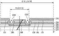
图1是例示了基于边框弯曲的常规柔性显示装置的平面视图,图2是例示了图1中的区域A的放大视图,图3是沿着图1中所示的线I-I’截取的截面视图,图4是例示了图3中的弯曲区域弯曲的截面视图。1 is a plan view illustrating a conventional flexible display device based on bezel bending, FIG. 2 is an enlarged view illustrating an area A in FIG. 1 , and FIG. 3 is taken along line II' shown in FIG. 1 . Cross-sectional view, FIG. 4 is a cross-sectional view illustrating the bending of the bending region in FIG. 3 .
参照图1至图4,基于边框弯曲的常规柔性显示装置包括显示区域1、非显示区域2、弯曲区域3、面内栅极(GIP)区域4和驱动部5。1 to 4 , a conventional flexible display device based on bezel bending includes a
显示区域1是显示图像的区域,非显示区域2是不显示图像的区域。非显示区域2的一部分包括弯曲类型的弯曲区域3。GIP区域4是选通驱动电路被布置在形成有薄膜晶体管(TFT)基板的显示面板的内部的区域。The
显示区域1和非显示区域2包括基板25、聚酰亚胺层24、多阻挡层23、无机层22、栅绝缘层12、介电中间层21以及钝化层20。The
在这种情况下,薄膜晶体管T、平整层30、阳极40和辅助电极50形成在显示区域1上。薄膜晶体管T包括有源层11、栅绝缘膜12、栅极13、介电中间层14、源极15以及漏极16。In this case, the thin film transistor T, the
岸60形成在阳极40和辅助电极50上以限定像素区域,有机发光层70形成在由岸60限定的像素区域中,并且阴极80形成在有机发光层70上。The
在上述的常规柔性显示装置中,如图4中所示,弯曲区域4被弯曲以使与非显示区域2的一部分对应的边框最小化。此时,在从薄膜晶体管T连接的源极15中可能出现裂缝。因此,常规柔性显示装置使用具有与图2中的图案相同的形状的线来减少这种裂缝。In the above-described conventional flexible display device, as shown in FIG. 4 , the
然而,在这种情况下,源极15不被设置在中性平面上,凭此不能完全避免源极15中出现的裂缝。In this case, however, the
另外,在这种情况下,出现以下问题:由于如图2中所示的线之间的距离P以及这些线的宽度L,因此无法将图2中的线应用于高分辨率显示装置。这是因为,由于通过在高分辨率显示装置中相对地增加的线的距离P和宽度L而预留的区域,因此在线的设计方面存在局限性。In addition, in this case, there arises a problem that the lines in FIG. 2 cannot be applied to a high-resolution display device due to the distance P between the lines and the width L of the lines as shown in FIG. 2 . This is because, due to the area reserved by the relatively increased distance P and width L of the line in the high-resolution display device, there is a limitation in the design of the line.
发明内容SUMMARY OF THE INVENTION
因此,本公开涉及一种柔性显示装置,该柔性显示装置基本上避免了由于现有技术的局限性和缺点而导致的一个或更多个问题。Accordingly, the present disclosure is directed to a flexible display device that substantially obviates one or more of the problems due to limitations and disadvantages of the related art.
本公开的一个优点在于提供了一种能够防止在弯曲区域的线中出现裂缝的柔性显示装置。An advantage of the present disclosure is to provide a flexible display device capable of preventing cracks from appearing in lines of a bending region.
本公开的另一优点在于提供了一种通过使用直线而具有高分辨率的柔性显示装置。Another advantage of the present disclosure is to provide a flexible display device having high resolution by using straight lines.
本公开的另外的优点在于提供了一种通过使非显示区域的边框最小化而使其美观外形得到改进的柔性显示装置。An additional advantage of the present disclosure is to provide a flexible display device with an improved aesthetic appearance by minimizing bezels in non-display areas.
本发明另外的优点、目的和特征将在下面的描述中部分地进行阐述,并且对于阅读下面内容的本领域普通技术人员部分地将变得显而易见,或者可以通过本发明的实践来得到了解。可以通过书面的说明书及其权利要以及附图中具体指出的结构来实现和获得本发明的目的和其它优点。Additional advantages, objects and features of the present invention will be set forth, in part, in the description that follows, and in part will become apparent to those of ordinary skill in the art from reading the following, or may be learned by practice of the present invention. The objectives and other advantages of the invention may be realized and attained by the structure particularly pointed out in the written description and claims hereof as well as the appended drawings.
为了实现这些目的及其它优点并且根据本发明的目的,如本文中所具体实现并广义描述的,在一种实施方式中,一种柔性显示装置包括:基板,该基板包括显示图像的显示区域和不显示图像的非显示区域,所述非显示区域包括所述柔性显示装置能够进行弯曲的弯曲区域;链接线(link line),该链接线在所述基板上位于所述非显示区域中;第一缓冲层,该第一缓冲层在所述基板上位于所述弯曲区域中;弯曲连接线,该弯曲连接线在所述基板上位于所述弯曲区域中的所述第一缓冲层上,所述弯曲连接线在所述弯曲区域中与所述链接线连接;以及第二缓冲层,该第二缓冲层在所述基板的所述弯曲区域中位于所述弯曲连接线上。To achieve these objects and other advantages and in accordance with the objects of the present invention, as embodied and broadly described herein, in one embodiment, a flexible display device includes a substrate including a display area displaying an image and a non-display area where no image is displayed, the non-display area including a bending area where the flexible display device can be bent; a link line, the link line being located in the non-display area on the substrate; a buffer layer, the first buffer layer is located on the substrate in the bending region; a curved connecting line is located on the substrate on the first buffer layer in the bending region, so the curved connecting line is connected with the linking line in the curved region; and a second buffer layer located on the curved connecting line in the curved region of the substrate.
在另一实施方式中,一种柔性显示装置包括:基板,该基板包括显示图像的显示区域和不显示图像的非显示区域,所述非显示区域包括所述柔性显示装置能够进行弯曲的弯曲区域;薄膜晶体管(TFT),该TFT位于所述显示区域中,所述TFT包括位于所述柔性显示装置的第一层中的电极;弯曲连接线,该弯曲连接线位于所述非显示区域的所述弯曲区域中,所述弯曲连接线位于所述柔性显示装置的第二层中,所述柔性显示装置的所述第二层位于包括所述TFT的所述电极的所述第一层下方;链接线,该链接线位于所述非显示区域中,所述链接线经由至少一个接触孔使所述TFT的在所述第一层中的所述电极和位于所述第二层中的所述弯曲连接线电连接在一起;以及第一缓冲层和第二缓冲层,所述弯曲连接线在所述弯曲区域中位于所述第一缓冲层和所述第二缓冲层之间。In another embodiment, a flexible display device includes: a substrate including a display area displaying an image and a non-display area not displaying an image, the non-display area including a bending area where the flexible display device can bend ; thin film transistors (TFTs) located in the display area, the TFTs comprising electrodes located in the first layer of the flexible display device; curved connecting lines located in all parts of the non-display area In the bending region, the bending connecting line is located in a second layer of the flexible display device, and the second layer of the flexible display device is located under the first layer including the electrodes of the TFT; a link line located in the non-display area, the link line connecting the electrode in the first layer and the electrode in the second layer of the TFT via at least one contact hole Bending connection lines are electrically connected together; and first and second buffer layers, the bending connection lines being located between the first buffer layer and the second buffer layer in the bending region.
应该理解的是,对本发明的以上一般描述和以下详细描述都是示例性和解释性的,并且旨在对所要求保护的本发明提供进一步的解释。It is to be understood that both the foregoing general description and the following detailed description of the present invention are exemplary and explanatory and are intended to provide further explanation of the invention as claimed.
附图说明Description of drawings
附图被包括以提供对本发明的进一步理解,被并入到本申请中并构成本申请的一部分,附图例示了本发明的实施方式,并且与本说明书一起用于解释本发明的原理。在附图中:The accompanying drawings, which are included to provide a further understanding of the invention, are incorporated in and constitute a part of this application, illustrate embodiments of the invention, and together with the description serve to explain the principles of the invention. In the attached image:
图1是例示常规柔性显示装置的正面视图;FIG. 1 is a front view illustrating a conventional flexible display device;
图2是例示图1中的区域A的放大视图;FIG. 2 is an enlarged view illustrating a region A in FIG. 1;
图3是沿着图1中所示的线I-I’截取的截面视图;Figure 3 is a cross-sectional view taken along the line II' shown in Figure 1;
图4是例示常规柔性显示装置弯曲的截面视图;4 is a cross-sectional view illustrating bending of a conventional flexible display device;
图5是例示根据本公开的柔性显示装置的正面视图;FIG. 5 is a front view illustrating a flexible display device according to the present disclosure;
图6是根据本公开的一个实施方式的沿着图5中所示的线II-II’截取的截面视图;Figure 6 is a cross-sectional view taken along line II-II' shown in Figure 5 according to one embodiment of the present disclosure;
图7是根据本公开的另一实施方式的沿着图5中所示的线II-II’截取的截面视图;Figure 7 is a cross-sectional view taken along line II-II' shown in Figure 5 according to another embodiment of the present disclosure;
图8是例示根据本公开的柔性显示装置的中性平面的视图;FIG. 8 is a view illustrating a neutral plane of a flexible display device according to the present disclosure;
图9A、图9B和图9C是例示根据本公开的用于确定柔性显示装置的厚度的实验的视图;以及9A, 9B, and 9C are views illustrating an experiment for determining the thickness of a flexible display device according to the present disclosure; and
图10是例示根据本公开的柔性显示装置弯曲的截面视图。FIG. 10 is a cross-sectional view illustrating bending of the flexible display device according to the present disclosure.
具体实施方式Detailed ways
通过参照附图描述的如下实施方式,将阐明本公开的优点和特征及其实现方法。然而,本公开可以按照不同的形式来实施,并且不应当被理解为局限于本文中阐述的实施方式。相反,提供这些实施方式以使得本公开将彻底并完整,并且将本发明的范围充分地传达给本领域的技术人员。另外,本公开仅由权利要求的范围来限定。The advantages and features of the present disclosure and a method for realizing the same will be clarified by the following embodiments described with reference to the accompanying drawings. However, the present disclosure may be embodied in different forms and should not be construed as limited to the embodiments set forth herein. Rather, these embodiments are provided so that this disclosure will be thorough and complete, and will fully convey the scope of the invention to those skilled in the art. Additionally, the present disclosure is to be limited only by the scope of the claims.
为了描述本发明的实施方式而在附图中公开的形状、尺寸、比率、角度和数字仅仅是示例,并因此本发明不限于所例示的细节。相同的附图标记在整个说明书中表示相同的元件。在下面的描述中,当确定相关已知功能或配置的详细描述会不必要地使本发明的要点模糊不清时,将省略所述详细描述。在使用本说明书中描述的“包括”、“具有”和“包含”的情况下,除非使用“仅~”,否则还可添加其它部件。除非相反地指出,单数形式的术语可以包括复数形式。The shapes, dimensions, ratios, angles and numbers disclosed in the drawings for the purpose of describing embodiments of the present invention are merely examples, and thus the present invention is not limited to the illustrated details. The same reference numbers refer to the same elements throughout the specification. In the following description, when it is determined that the detailed description of related known functions or configurations would unnecessarily obscure the gist of the present invention, the detailed description will be omitted. In the case of using "including", "having" and "comprising" described in this specification, unless "only -" is used, other components may also be added. Unless indicated to the contrary, terms in the singular may include the plural.
在对元件进行解释时,虽然没有明确的说明,但是元件也被解释为包括误差范围。When an element is explained, although not explicitly stated, the element is also explained to include a range of error.
在本公开的实施方式的描述中,当一个结构(例如,电极、线、接线、层或者触点)被描述为形成在另一结构的上部/下部或者在另一结构上面/下面时,该描述应当被理解为包括这些结构彼此接触的情况、以及在其中设置有第三结构的情况。In the description of embodiments of the present disclosure, when a structure (eg, electrode, wire, wire, layer, or contact) is described as being formed on/under or above/under another structure, the The description should be understood to include the case where these structures are in contact with each other, as well as the case where a third structure is provided therein.
当描述时间关系时,例如当时间顺序被描述为“在~之后”、“继~之后”、“靠近~”和“在~之前”时,除非使用“正好”或“恰好”,否则还可以包括不连续的情况。When describing a temporal relationship, such as when chronological order is described as "after ~", "following ~", "near ~" and "before ~", unless "just" or "just" is used, it is also possible to Including discontinuities.
将要理解的是,尽管术语第一、第二等可以在本文中被用来描述各个元件,但是这些元件不应当受到这些术语的限制。这些术语仅被用来将一个元件与另一元件区分开。例如,在不背离本发明的范围的情况下,第一元件可以被称为第二元件,并且类似地,第二元件可以被称为第一元件。It will be understood that, although the terms first, second, etc. may be used herein to describe various elements, these elements should not be limited by these terms. These terms are only used to distinguish one element from another. For example, a first element could be termed a second element, and, similarly, a second element could be termed a first element, without departing from the scope of the present invention.
本公开的各种实施方式的特征可以部分地或全部地彼此进行结合或组合,并且可以与彼此进行各种互相操作并在技术上如本领域技术人员能够充分理解的那样进行驱动。本公开的实施方式可以彼此独立地执行,或者可以在相互依赖的关系中一起执行。The features of the various embodiments of the present disclosure may be combined or combined with each other in part or in whole, and may be variously interoperable with each other and driven as technically well understood by those skilled in the art. The embodiments of the present disclosure may be performed independently of each other or may be performed together in an interdependent relationship.
在下文中,将参照附图详细地描述本公开的优选实施方式。Hereinafter, preferred embodiments of the present disclosure will be described in detail with reference to the accompanying drawings.
图5是例示根据本发明的柔性显示装置的正面视图,图6是沿着图5中所示的线II-II’截取的截面视图。5 is a front view illustrating a flexible display device according to the present invention, and FIG. 6 is a cross-sectional view taken along line II-II' shown in FIG. 5 .
参照图5、图6和图7,根据本公开的柔性显示装置包括显示区域1、非显示区域2、驱动膜5和GIP区域4。非显示区域2包括弯曲区域3。首先,将描述显示区域1,接下来将描述非显示区域2和弯曲区域3。5 , 6 and 7 , the flexible display device according to the present disclosure includes a
显示区域1包括位于基板210上的第一缓冲层220、无机层230、第二缓冲层240、多缓冲层250、薄膜晶体管T、钝化层270、平整层180、阳极185、辅助电极190、岸层(banklayer)200、有机发光层203和阴极207。The
基板210可以是塑料膜。例如,基板210可以是非限制性地包括下面的项在内的片材或膜:诸如TAC(三醋酸纤维素)或DAC(二醋酸纤维素)这样的纤维素树脂,诸如降冰片烯衍生物这样的COP(环烯烃聚合物),COC(环烯烃共聚物),诸如PMMA(聚甲基丙烯酸甲酯)这样的丙烯酸树脂,诸如PC(聚碳酸酯)、PE(聚乙烯)或PP(聚丙烯)、PVA(聚乙烯醇)这样的聚烯烃,诸如PES(聚醚砜)、PEEK(聚醚醚酮)、PEI(聚醚酰亚胺)、PEN(聚萘二甲酸乙二醇酯)和PET(聚对苯二甲酸乙二醇酯)、PI(聚酰亚胺)、PSF(聚砜)这样的聚酯纤维,或者氟树脂。The
第一缓冲层220被布置在基板210上,并且可以非限制性地由PI(聚酰亚胺)制成。在本公开中,由于第一缓冲层220是用于构成中性平面的元件,第一缓冲层220将在弯曲区域3中更详细地进行描述。The
无机层230可以由包含氧化物和氮化物的材料制成,并且可以由诸如硅氮化物(SiNx)、硅氧化物(SiOx)、钛氧化物(TiOx)、铝氧化物(AlOx)、铟镓氧化物(IGO)、铟锌氧化物(IZO)和铟镓锌氧化物(IGZO)这样的无机材料制成。无机层230可以用来防止水渗透到其中。无机层230可以直接位于第一缓冲层220上,使得第一缓冲层220直接位于无机层230下面。The
第二缓冲层240被布置在基板210上方,并且可以非限制性地由PI(聚酰亚胺)制成。在本公开中,由于第二缓冲层240是用于构成中性平面的元件,第二缓冲层240将在弯曲区域3中更详细地进行描述。The
多缓冲层250可以由包含诸如硅Si、铝Al、钡Ba、钼Mo、铜Cu、钛Ti和锌Zn这样的金属材料的氧化物和氮化物在内的无机材料制成。多缓冲层250用来防止基板210中包含的材料在薄膜晶体管T的制造过程的高温处理期间扩散到薄膜晶体管T中。另外,多缓冲层250可以用来防止外部的水或湿气渗透到透明的柔性显示装置中。因此,除了透明柔性显示装置的诸如第二缓冲层240的其它特征以外,多缓冲层250还具有更高的耐水性。The
薄膜晶体管T包括有源层110、栅绝缘膜120、栅极130、介电中间层140、源极150以及漏极160。The thin film transistor T includes an
有源层110形成在基板210上,以与栅极130交叠。有源层110可以由基于硅的半导体材料或基于氧化物的半导体材料制成。如图7中所示,遮光层284和有源缓冲层290可以附加地形成在基板210和有源层110之间。在这种情况下,通过基板210的下表面入射的外部光可以被遮光层284遮挡,据此可以防止有源层110受到外部光的损害。The
栅绝缘膜120形成在有源层110上。栅绝缘膜120用来使有源层110与栅极130隔离。栅绝缘膜120可以由无机绝缘材料制成,例如可以非限制性地由硅氧化物(SiOX)膜、硅氮化物(SiNX)膜或者多层SiOX和SiNX形成。栅绝缘膜120可以延伸到非显示区域2。The
栅极130形成在栅绝缘膜120上。栅极130形成为通过插入在该栅极130与有源层110之间的栅绝缘膜120来与该有源层110交叠。栅极130可以是但不限于由Mo、Al、Cr、Au、Ti、Ni、Nd和Cu中的任何一个或者它们的合金组成的单层或多层。The
介电中间层140形成在栅极130上。介电中间层140可以由与栅绝缘膜120的无机绝缘材料相同的无机绝缘材料制成,例如可以非限制性地由硅氧化物(SiOX)膜、硅氮化物(SiNX)膜或者多层SiOX和SiNX形成。A
源极150和漏极160彼此面对地形成在介电中间层140上。上述的栅绝缘膜120和上述的介电中间层140设置有第一接触孔CH1和第二接触孔CH2,其中,第一接触孔CH1使有源层110的一端区域露出,第二接触孔CH2使有源层110的另一端区域露出。源极150穿过第二接触孔CH2与有源层110的另一端区域连接,漏极160穿过第一接触孔CH1与有源层110的一端区域连接。另外,源极150可以延伸到非显示区域2,然后与第一链接线151连接。The
上述薄膜晶体管T可以被修改为本领域技术人员所知的各种结构,而不限制于如所示的上述结构。例如,虽然薄膜晶体管T形成在附图中的栅极130形成在有源层110上方的顶栅结构中,但是薄膜晶体管T也可以形成在栅极130形成在有源层110下方的底栅结构中。The above-mentioned thin film transistor T may be modified into various structures known to those skilled in the art, and is not limited to the above-mentioned structure as shown. For example, although the thin film transistor T is formed in the top gate structure in which the
钝化层270形成在薄膜晶体管T上,更具体地形成在源极150和漏极160上。钝化层270用来保护薄膜晶体管T,并且可以非限制性地由例如SiOX或SiNX的无机绝缘材料制成。The
平整层180形成在钝化层270上。平整层180用来使基板210的设置有薄膜晶体管T的上部平整。平整层180可以非限制性地由诸如丙烯酸树脂、环氧树脂、酚醛树脂、聚酰胺树脂和聚酰胺树脂这样的有机绝缘材料制成。The
阳极185形成在平整层180上。上述的钝化层270和上述的平整层180设置有使源极150露出的第三接触孔CH3,并且源极150和阳极185经由第三接触孔CH3彼此连接。The
辅助电极190形成在与阳极185相同的层上。辅助电极190用来减小稍后将描述的阴极207的电阻。The
岸层200形成在平整层180的一个表面处,并且形成在阳极185的两个边缘和辅助电极190的两个边缘上面。平整层180包括第三接触孔CH3,第三接触孔CH3使源极150从钝化层270和平整层180露出。岸层200可以防止水渗透到透明的柔性显示装置中。岸层200可以非限制性地由诸如聚酰亚胺树脂、丙烯酸树脂和BCB这样的有机绝缘材料制成。The
虽然未示出,有机发光层203可以形成在空穴注入层、空穴传输层、有机发光层、电子传输层和电子注入层依次进行沉积的结构中。在这种情况下,可以省略空穴注入层、空穴传输层、电子传输层和电子注入层中的一个或两个或更多个。有机发光层可以形成为针对每个像素发出相同颜色的光(例如,白色光),或者可以形成为针对每个像素发出不同颜色的光(例如,红色光、绿色光和蓝色光)。Although not shown, the organic
阴极207形成在有机发光层203上。由于阴极207形成在发出光的表面上,因此阴极207是由透明的导电材料制成的。由于阴极207由透明导电材料制成,因此阴极207具有高的电阻。因此,为了减小阴极207的电阻,阴极207与辅助电极190连接。阴极207可以通过诸如溅射这样的沉积处理来形成,沉积处理不具有沉积材料的良好的线性度。The
虽然未示出,包封层可以附加地形成在阴极207上,以防止发生水渗透。本领域中已知的各种材料都可以用作包封层。另外,虽然未示出,但是可以在阴极207上附加地形成针对每个像素的滤色器。在这种情况下,有机发光层203可以发出白色光。Although not shown, an encapsulation layer may be additionally formed on the
接下来,在GIP区域4中,相应的层被形成为与显示区域1对应,并且多个驱动装置和电力线形成在栅绝缘膜120上。另外,GIP区域4中的无机层230可以设置有遮光层282,该遮光层282通过与稍后将要描述的弯曲连接线280的处理相同的处理来形成在与弯曲连接线280相同的层上。然而,不限制于该示例,遮光层282可以形成在显示区域1、非显示区域2和GIP区域4中的任何一个区域中。Next, in the
接下来,驱动膜5被布置为与非显示区域2平行,并且将用于显示图像的电信号传送到显示区域。驱动膜5与稍后将要描述的第二链接线153连接。也就是说,电路板(未示出)可以形成在驱动膜5的与外部系统(未示出)连接的一端,据此显示区域1与外部系统电连接。Next, the driving
接下来,将更详细地描述根据本公开的柔性显示装置的非显示区域2和弯曲区域3。将省略显示区域1的重复描述。Next, the
根据本公开的柔性显示装置的非显示区域2和弯曲区域3还包括第四接触孔CH4、第五接触孔CH5、弯曲连接线280、第一链接线151和第二链接线153。另外,非显示区域2中的无机层230可以设置有遮光层,该遮光层通过与弯曲连接线280的处理相同的处理来形成在与弯曲连接线280相同的层上。The
显示区域的源极150延伸到第一链接线151,据此第一链接线151穿过第四接触孔CH4与弯曲区域的弯曲连接线280的一端(例如,第一端)电连接。弯曲连接线280的另一端(例如,第二端)穿过第五接触孔CH5与第二链接线153连接,该第二链接线153与焊盘部连接。另外,第一链接线151和第二链接线153可以被布置为在柔性显示装置如图10中所示地在弯曲区域中弯曲的同时彼此平行。The source electrode 150 of the display region extends to the
无机层230可以包括第一无机层和第二无机层。弯曲连接线280可以在弯曲区域处形成在第一无机层上。然后,第二无机层可以形成在第一无机层和弯曲连接线280上。因此,弯曲连接线280被布置为由无机层230包围。The
另外,无机层230设置在第一缓冲层220和第二缓冲层240之间,使得第一缓冲层220直接在无机层230下面并且第二缓冲层240直接在无机层230上。In addition, the
第一缓冲层220和第二缓冲层240可以通过在它们之间插入无机层230以相同的厚度由相同的材料(诸如聚酰亚胺)形成。然而,第一缓冲层220和第二缓冲层240可以由诸如TAC(三醋酸纤维素)或DAC(二醋酸纤维素)这样的纤维素树脂、诸如降冰片烯衍生物这样的COP(环烯烃聚合物)、COC(环烯烃共聚物)、诸如PMMA(聚甲基丙烯酸甲酯)这样的丙烯酸树脂、诸如PC(聚碳酸酯)、PE(聚乙烯)或PP(聚丙烯)、PVA(聚乙烯醇)这样的聚烯烃、PES(聚醚砜)、PEEK(聚醚醚酮)、PEI(聚醚酰亚胺)、PEN(聚萘二甲酸乙二醇酯)和PET(聚对苯二甲酸乙二醇酯)等制成,而不限制于聚酰亚胺。The
如上所述,与常规的柔性显示装置不同,与第一链接线151和第二链接线153连接的弯曲连接线280被布置在第一缓冲层220和第二缓冲层240之间,由此能够获得具有线性线结构的高分辨率柔性显示装置。As described above, unlike the conventional flexible display device, the
由于弯曲连接线280布置在第一缓冲层220和第二缓冲层240之间,因此在弯曲连接线280上形成有中性平面。中性平面是指当向其施加弯曲力矩时,在保持其原始长度不增大或减小的情况下仅弯曲的平面。也就是说,中性平面是指通过使在弯曲期间施加给弯曲连接线的拉伸应力和压缩应力抵消来使最小力施加到弯曲表面的平面。Since the
另外,当向对象施加弯曲力矩时出现的中性平面NP形成在该对象的中部。因此,可能的话,如果通过在其之间插入线而布置的上部和下部具有彼此相同的厚度和相同的特性,则形成要由在向柔性显示装置施加弯曲力矩时出现的中性平面NP进行保护的线。In addition, a neutral plane NP that appears when a bending moment is applied to an object is formed in the middle of the object. Therefore, if possible, if the upper and lower parts arranged by inserting wires therebetween have the same thickness and the same characteristics as each other, it is formed to be protected by the neutral plane NP that occurs when a bending moment is applied to the flexible display device line.
在下文中,将参照图8来描述在根据本公开的柔性显示装置的第一缓冲层220和第二缓冲层240以及弯曲连接线280中形成的中性平面。Hereinafter, the neutral plane formed in the
图8是例示在根据本公开的柔性显示装置的弯曲区域中形成的中性平面的视图。中性平面NP形成在图8中所示的弯曲连接线280的中心处。此时,箭头方向上的力从垂直方向上所示的虚线被传送到与对角线方向上的虚线相切的直线。在这种情况下,基于中性平面NP的上部箭头代表拉伸应力,而基于中性平面NP的下部箭头代表压缩应力。如果反复地或者以断裂强度或更强的强度来施加该拉伸应力和压缩应力,则柔性显示装置中形成的线可能受到损害或缩短。FIG. 8 is a view illustrating a neutral plane formed in a bending region of the flexible display device according to the present disclosure. The neutral plane NP is formed at the center of the curved connecting
在这方面,在根据本公开的柔性显示装置中,为了使边框最小化并且防止弯曲区域3中设置的弯曲连接线280受到损害,在弯曲区域3上的每一层的厚度可以被确定为使得中性平面可以设置在弯曲连接线280上。In this regard, in the flexible display device according to the present disclosure, in order to minimize the bezel and prevent the
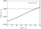
图9A和图9B例示了用于确定根据本公开的柔性显示装置的基板和缓冲层的厚度的实验。图9C例示了根据本发明的柔性显示装置的每一层的厚度是基于上述实验来设置的。9A and 9B illustrate experiments for determining the thicknesses of substrates and buffer layers of a flexible display device according to the present disclosure. 9C illustrates that the thickness of each layer of the flexible display device according to the present invention is set based on the above experiments.
图9A和图9B中的曲线图中的轴线X是指出现中性平面的距离,轴线Y分别代表应力和应变。通过图9A和图9B中所示的这种仿真的分析方法基于关于杨氏模量(E)、泊松比(v)、厚度(d)、应变(ε)和层总厚度(h)的中性平面理论。Axis X in the graphs of Figures 9A and 9B refers to the distance at which the neutral plane occurs, and axis Y represents stress and strain, respectively. The analytical method by this simulation shown in Figures 9A and 9B is based on the Young's modulus (E), Poisson's ratio (v), thickness (d), strain (ε) and total layer thickness (h) Neutral plane theory.
参照图9A和图9B,当包括基板的厚度在内的要到达弯曲连接线280的总厚度为60.1μm或60.2μm时,中性平面可以形成在弯曲连接线280上。也就是说,如果线被布置在包括基板的厚度在内的要到达弯曲连接线280的总厚度为60.1μm或60.2μm的点处,则为了保护该点,最小应变作用在该点上。因此,使用该点作为目标点来布置弯曲连接线280。9A and 9B , when the total thickness to reach the
参照图9C,当基板210的厚度被设计为50μm,第一缓冲层220的厚度被设计为10μm,无机层230的厚度被设计为0.1μm,第二缓冲层240的厚度被设计为10μm并且多缓冲层250的厚度被设计为1.2μm,并且弯曲连接线280布置在无机层230上时,中性平面可以形成在弯曲连接线280上。也就是说,当根据本公开的柔性显示装置的每一层的厚度如图9C中所示时,中性平面形成在弯曲连接线280上,由此弯曲连接线280即使在弯曲的情况下也既不会受到损害,又不会缩短。然而,上述厚度仅仅是示例性的,并且中性平面的位置可以取决于基板的厚度或特性以及第一缓冲层220和第二缓冲层240的厚度或特性而改变。因此,可以使用可以由本领域普通技术人员容易地设计的厚度值来设计期望的中性平面。例如,第一缓冲层220和第二缓冲层240可以被设计为具有彼此相同的厚度和相同的特性。9C , when the thickness of the
另外,如图8中所示通过蚀刻在弯曲区域3中形成岛图案(island pattern)。与无机单层结构相比,该岛图案结构可以减小应力的集中水平,由此可以降低裂缝的发生率。虽然示出了一个岛图案结构,但是岛图案结构不限于所示的结构。例如,可以通过蚀刻来形成多个岛图案。In addition, an island pattern is formed in the
图10是例示根据本公开的柔性显示装置的弯曲区域弯曲的截面视图。FIG. 10 is a cross-sectional view illustrating bending of a bending region of a flexible display device according to the present disclosure.
如将要从图10中知道的,压缩应力和拉伸应力被抵消的中性平面形成在弯曲区域3中的弯曲连接线280上,由此弯曲连接线280既不会受到损害又不会缩短。另外,根据本公开的柔性显示装置的弯曲连接线280可以被用于通过形成直线结构而使线之间的间距减小的高分辨率柔性显示装置。另外,由于柔性显示装置的与非显示区域2对应的边框可以由于弯曲区域3的弯曲而变薄,因此可以获得美观外形得到改进的柔性显示装置。As will be known from FIG. 10 , a neutral plane in which compressive and tensile stresses are canceled is formed on the curved connecting
如上所述,根据本公开,能够获得以下优点。As described above, according to the present disclosure, the following advantages can be obtained.
首先,能够获得能够防止在弯曲区域的线中出现裂缝的柔性显示装置。First, it is possible to obtain a flexible display device capable of preventing cracks from occurring in the lines of the bending regions.
其次,能够通过使用直线来获得高分辨率的柔性显示装置。Second, a high-resolution flexible display device can be obtained by using straight lines.
最后,能够通过使非显示区域的边框最小化来获得美观外形得到改进的柔性显示装置。Finally, a flexible display device with an improved aesthetic appearance can be obtained by minimizing the bezel of the non-display area.
对于本领域技术人员将显而易见的是,能够在不背离本发明的精神或范围的情况下对本发明做出各种修改和改变。因此,本发明旨在本发明的涵盖落入所附的权利要求及其等同物的范围内的修改和变型。It will be apparent to those skilled in the art that various modifications and variations can be made in the present invention without departing from the spirit or scope of the inventions. Therefore, it is intended that the present invention covers the modifications and variations that come within the scope of the appended claims and their equivalents.
相关申请的交叉引用CROSS-REFERENCE TO RELATED APPLICATIONS
本申请要求于2015年12月15日提交的韩国专利申请No.10-2015-0178916的权益,该韩国专利申请通过引用方式完整地被并入到本文中。This application claims the benefit of Korean Patent Application No. 10-2015-0178916, filed on December 15, 2015, which is incorporated herein by reference in its entirety.
Claims (20)
Translated fromChinesePriority Applications (1)
| Application Number | Priority Date | Filing Date | Title |
|---|---|---|---|
| CN202010380482.3ACN111540772B (en) | 2015-12-15 | 2016-06-01 | Flexible display device |
Applications Claiming Priority (2)
| Application Number | Priority Date | Filing Date | Title |
|---|---|---|---|
| KR10-2015-0178916 | 2015-12-15 | ||
| KR1020150178916AKR102611499B1 (en) | 2015-12-15 | 2015-12-15 | Flexible display device |
Related Child Applications (1)
| Application Number | Title | Priority Date | Filing Date |
|---|---|---|---|
| CN202010380482.3ADivisionCN111540772B (en) | 2015-12-15 | 2016-06-01 | Flexible display device |
Publications (2)
| Publication Number | Publication Date |
|---|---|
| CN106887447A CN106887447A (en) | 2017-06-23 |
| CN106887447Btrue CN106887447B (en) | 2020-06-16 |
Family
ID=57460443
Family Applications (2)
| Application Number | Title | Priority Date | Filing Date |
|---|---|---|---|
| CN201610380459.8AActiveCN106887447B (en) | 2015-12-15 | 2016-06-01 | flexible display device |
| CN202010380482.3AActiveCN111540772B (en) | 2015-12-15 | 2016-06-01 | Flexible display device |
Family Applications After (1)
| Application Number | Title | Priority Date | Filing Date |
|---|---|---|---|
| CN202010380482.3AActiveCN111540772B (en) | 2015-12-15 | 2016-06-01 | Flexible display device |
Country Status (5)
| Country | Link |
|---|---|
| US (5) | US10224344B2 (en) |
| EP (1) | EP3182473B1 (en) |
| JP (1) | JP6616273B2 (en) |
| KR (3) | KR102611499B1 (en) |
| CN (2) | CN106887447B (en) |
Families Citing this family (129)
| Publication number | Priority date | Publication date | Assignee | Title |
|---|---|---|---|---|
| US9515099B2 (en)* | 2014-07-31 | 2016-12-06 | Lg Display Co., Ltd. | Flexible display device with wire having reinforced portion and manufacturing method for the same |
| KR102611499B1 (en)* | 2015-12-15 | 2023-12-06 | 엘지디스플레이 주식회사 | Flexible display device |
| KR102627284B1 (en)* | 2016-05-12 | 2024-01-22 | 엘지디스플레이 주식회사 | Method of manufacturing a connection structure connecting cathode electrode to auxiliary cathode electrode, and organic light emitting diode display device using the same |
| KR102589214B1 (en)* | 2016-06-03 | 2023-10-13 | 삼성디스플레이 주식회사 | Display device |
| KR102604018B1 (en)* | 2016-07-07 | 2023-11-22 | 삼성디스플레이 주식회사 | Display device |
| KR102535363B1 (en)* | 2016-07-11 | 2023-05-24 | 삼성디스플레이 주식회사 | Display panel and display apparatus including thereof |
| KR102651930B1 (en)* | 2016-07-29 | 2024-03-27 | 엘지디스플레이 주식회사 | Organic light emitting display device and method of manufacturing the same |
| KR102597681B1 (en) | 2016-09-19 | 2023-11-06 | 삼성디스플레이 주식회사 | Display device |
| KR102729661B1 (en)* | 2016-09-22 | 2024-11-13 | 삼성디스플레이 주식회사 | Display device and manufacturing method thereof |
| KR102659422B1 (en)* | 2016-10-17 | 2024-04-22 | 삼성디스플레이 주식회사 | Organic light emitting diode display and method for manufacturing the same |
| KR102743728B1 (en) | 2016-11-08 | 2024-12-19 | 삼성디스플레이 주식회사 | Display device |
| KR102787595B1 (en)* | 2017-01-10 | 2025-04-01 | 삼성디스플레이 주식회사 | Display device |
| KR102772195B1 (en)* | 2017-02-28 | 2025-02-26 | 삼성디스플레이 주식회사 | Display apparatus and method for manufacturing the same |
| KR102373441B1 (en) | 2017-03-31 | 2022-03-14 | 삼성디스플레이 주식회사 | Display apparatus |
| JP2018180413A (en)* | 2017-04-19 | 2018-11-15 | 株式会社ジャパンディスプレイ | Display device and method of manufacturing display device |
| CN107293553B (en)* | 2017-06-19 | 2020-11-24 | 京东方科技集团股份有限公司 | Array substrate and preparation method thereof, display panel and display device |
| KR102370450B1 (en) | 2017-07-07 | 2022-03-04 | 삼성디스플레이 주식회사 | Display device |
| KR102370406B1 (en) | 2017-07-10 | 2022-03-07 | 삼성디스플레이 주식회사 | Organic light emitting display device and a method of manufacturing organic light emitting display device |
| KR102432386B1 (en)* | 2017-07-12 | 2022-08-12 | 삼성디스플레이 주식회사 | Display device |
| JP2019020463A (en)* | 2017-07-12 | 2019-02-07 | 株式会社ジャパンディスプレイ | Display device and method of manufacturing display device |
| WO2019026237A1 (en)* | 2017-08-03 | 2019-02-07 | シャープ株式会社 | Display device |
| WO2019026285A1 (en)* | 2017-08-04 | 2019-02-07 | シャープ株式会社 | Display device |
| KR102393377B1 (en) | 2017-08-07 | 2022-05-03 | 삼성디스플레이 주식회사 | Display device |
| US10644096B2 (en) | 2017-08-22 | 2020-05-05 | Sharp Kabushiki Kaisha | Display device |
| CN107565049B (en)* | 2017-08-25 | 2019-11-01 | 京东方科技集团股份有限公司 | AMOLED display panel and preparation method thereof |
| CN107331694B (en)* | 2017-09-04 | 2020-03-17 | 京东方科技集团股份有限公司 | OLED display panel, preparation method thereof and OLED display device |
| JP2019050136A (en)* | 2017-09-11 | 2019-03-28 | 株式会社ジャパンディスプレイ | Display device and method of manufacturing display device |
| WO2019053784A1 (en)* | 2017-09-12 | 2019-03-21 | シャープ株式会社 | Display device |
| KR102449218B1 (en)* | 2017-09-19 | 2022-09-30 | 삼성디스플레이 주식회사 | display device |
| US10811488B2 (en)* | 2017-09-22 | 2020-10-20 | Sharp Kabushiki Kaisha | Display device |
| CN107845643B (en)* | 2017-09-25 | 2020-09-08 | 上海天马微电子有限公司 | A display panel and display device |
| KR102481385B1 (en)* | 2017-09-27 | 2022-12-27 | 삼성디스플레이 주식회사 | Foldable display apparatus and the manufacturing method thereof |
| CN111149429B (en)* | 2017-09-28 | 2022-10-04 | 夏普株式会社 | display device |
| WO2019064414A1 (en)* | 2017-09-28 | 2019-04-04 | シャープ株式会社 | Display device and production method for same |
| KR102417112B1 (en)* | 2017-09-28 | 2022-07-06 | 삼성디스플레이 주식회사 | Display apparatus |
| WO2019064534A1 (en)* | 2017-09-29 | 2019-04-04 | シャープ株式会社 | Flexible display device and production method for flexible display device |
| US11239453B2 (en)* | 2017-10-12 | 2022-02-01 | Sharp Kabushiki Kaisha | Non-flexible substrate having base layer including inorganic film between resin layers, flexible display device and method for producing same |
| JP7064846B2 (en)* | 2017-10-23 | 2022-05-11 | 株式会社ジャパンディスプレイ | Display device and manufacturing method of display device |
| CN107958920B (en)* | 2017-11-23 | 2020-10-09 | 合肥鑫晟光电科技有限公司 | Flexible display panel, flexible display device and preparation method thereof |
| JP6917873B2 (en)* | 2017-11-24 | 2021-08-11 | 株式会社ジャパンディスプレイ | Display device |
| JP2019095646A (en)* | 2017-11-24 | 2019-06-20 | 株式会社ジャパンディスプレイ | Display device and display device manufacturing method |
| US10269830B1 (en)* | 2017-11-27 | 2019-04-23 | Wuhan China Star Optoelectronics Semiconductor Display Technology Co., Ltd. | Flexible array substrate and manufacturing method thereof |
| KR102018754B1 (en)* | 2017-11-29 | 2019-09-05 | 엘지디스플레이 주식회사 | Flexible display device |
| KR102465788B1 (en) | 2017-11-30 | 2022-11-09 | 엘지디스플레이 주식회사 | Organic light emitting display device |
| KR102416038B1 (en) | 2017-11-30 | 2022-07-04 | 삼성디스플레이 주식회사 | Display device and manufacturing method thereof |
| CN109860203B (en)* | 2017-11-30 | 2020-11-17 | 昆山国显光电有限公司 | Array substrate, manufacturing method thereof and display screen |
| JP7086582B2 (en)* | 2017-12-11 | 2022-06-20 | 株式会社ジャパンディスプレイ | Display device |
| KR102452529B1 (en)* | 2017-12-12 | 2022-10-11 | 삼성디스플레이 주식회사 | Flexible substrate and display device including the same |
| KR102559510B1 (en)* | 2017-12-15 | 2023-07-24 | 엘지디스플레이 주식회사 | Display device |
| JP7077001B2 (en)* | 2017-12-15 | 2022-05-30 | 株式会社ジャパンディスプレイ | Display device |
| KR102104981B1 (en) | 2017-12-19 | 2020-05-29 | 엘지디스플레이 주식회사 | Display device |
| KR102126553B1 (en)* | 2017-12-19 | 2020-06-24 | 엘지디스플레이 주식회사 | Display device |
| KR102185116B1 (en)* | 2017-12-19 | 2020-12-01 | 엘지디스플레이 주식회사 | Display device |
| KR102126552B1 (en) | 2017-12-19 | 2020-06-24 | 엘지디스플레이 주식회사 | Display device |
| CN111201485A (en)* | 2017-12-22 | 2020-05-26 | 深圳市柔宇科技有限公司 | Flexible screen module and electronic device |
| KR102506258B1 (en)* | 2017-12-29 | 2023-03-03 | 엘지디스플레이 주식회사 | Display apparatus |
| JP2019124792A (en) | 2018-01-15 | 2019-07-25 | 株式会社ジャパンディスプレイ | Display device |
| WO2019150438A1 (en)* | 2018-01-30 | 2019-08-08 | シャープ株式会社 | Display device |
| US10566555B2 (en)* | 2018-01-30 | 2020-02-18 | Wuhan China Star Optoelectronics Semiconductor Display Technology Co., Ltd. | Organic light emitting diode (OLED) display panel and the manufacturing method thereof |
| TWI795523B (en) | 2018-02-05 | 2023-03-11 | 日商Jsr股份有限公司 | Wiring components |
| CN108267900B (en)* | 2018-02-08 | 2021-03-02 | 京东方科技集团股份有限公司 | Light valve structure and its manufacturing method, operating method, array substrate, electronic device |
| WO2019163030A1 (en)* | 2018-02-21 | 2019-08-29 | シャープ株式会社 | Display device and method of manufacture therefor |
| US20210005701A1 (en)* | 2018-03-02 | 2021-01-07 | Sharp Kabushiki Kaisha | Display device |
| KR102652448B1 (en) | 2018-03-13 | 2024-03-29 | 삼성디스플레이 주식회사 | Display apparatus |
| KR102491107B1 (en)* | 2018-03-16 | 2023-01-20 | 삼성전자주식회사 | Film packages, Chip on film packages and Package modules |
| US11380222B2 (en)* | 2018-03-27 | 2022-07-05 | Sharp Kabushiki Kaisha | Display device |
| CN111919512B (en)* | 2018-03-30 | 2023-08-15 | 夏普株式会社 | Display device |
| CN208077535U (en)* | 2018-04-28 | 2018-11-09 | 京东方科技集团股份有限公司 | A kind of flexible display panels and flexible display apparatus |
| US20210233438A1 (en)* | 2018-05-08 | 2021-07-29 | Huawei Technologies Co., Ltd. | Flexible display panel and mobile terminal |
| KR102601293B1 (en)* | 2018-05-08 | 2023-11-13 | 삼성디스플레이 주식회사 | Display device, test apparatus for display device and test method for display device |
| WO2019215863A1 (en)* | 2018-05-10 | 2019-11-14 | シャープ株式会社 | Display device |
| JP7098425B2 (en)* | 2018-06-06 | 2022-07-11 | 株式会社ジャパンディスプレイ | Display device |
| JP7062528B2 (en)* | 2018-06-14 | 2022-05-06 | 株式会社ジャパンディスプレイ | Semiconductor device |
| WO2020017014A1 (en)* | 2018-07-20 | 2020-01-23 | シャープ株式会社 | Display device |
| US10770667B2 (en)* | 2018-08-21 | 2020-09-08 | Wuhan China Star Optoelectronics Semiconductor Display Technology Co., Ltd. | Flexible display device and manufacturing method thereof |
| KR102531312B1 (en)* | 2018-08-24 | 2023-05-11 | 엘지디스플레이 주식회사 | Display Device |
| KR102687808B1 (en) | 2018-09-21 | 2024-07-25 | 삼성디스플레이 주식회사 | Display apparatus |
| KR102617925B1 (en) | 2018-09-27 | 2023-12-26 | 삼성디스플레이 주식회사 | Display device |
| CN109545796A (en)* | 2018-09-30 | 2019-03-29 | 武汉华星光电技术有限公司 | A kind of curved array substrate and preparation method thereof |
| KR102633093B1 (en)* | 2018-10-01 | 2024-02-05 | 삼성디스플레이 주식회사 | Display appratus and method of manufacturing the same |
| US10833135B2 (en)* | 2018-10-16 | 2020-11-10 | Wuhan China Star Optoelectronics Semiconductor Display Technology Co., Ltd. | Flexible organic light emitting diode display device and method of fabricating same |
| CN109360845A (en)* | 2018-10-24 | 2019-02-19 | 京东方科技集团股份有限公司 | Display substrate and preparation method thereof, display device and preparation method thereof, and display device |
| CN109192078B (en) | 2018-11-12 | 2021-01-26 | 京东方科技集团股份有限公司 | A flexible panel and its preparation method and display device |
| CN208938550U (en)* | 2018-11-26 | 2019-06-04 | 北京京东方技术开发有限公司 | Display panel and display device |
| KR102748388B1 (en)* | 2018-11-28 | 2025-01-02 | 삼성디스플레이 주식회사 | Display apparatus and method of manufacturing the same |
| CN109671718B (en)* | 2018-12-04 | 2021-02-23 | 武汉华星光电半导体显示技术有限公司 | Flexible display panel and manufacturing method thereof |
| CN109659345B (en)* | 2018-12-19 | 2021-02-26 | 武汉华星光电半导体显示技术有限公司 | Flexible OLED panel |
| KR102657036B1 (en)* | 2018-12-21 | 2024-04-11 | 엘지디스플레이 주식회사 | Display device |
| KR102664312B1 (en)* | 2018-12-24 | 2024-05-09 | 엘지디스플레이 주식회사 | Flexible display apparatus |
| KR102758895B1 (en)* | 2019-01-07 | 2025-01-24 | 삼성디스플레이 주식회사 | Display device and method of manufacturing the same |
| CN109887956B (en) | 2019-01-25 | 2021-04-27 | 武汉华星光电半导体显示技术有限公司 | Flexible array substrate of organic light emitting diode |
| KR20200094874A (en)* | 2019-01-30 | 2020-08-10 | 삼성디스플레이 주식회사 | Display device |
| CN109962177B (en)* | 2019-03-28 | 2020-08-11 | 京东方科技集团股份有限公司 | OLED substrate, preparation method thereof and OLED display device |
| CN110197845B (en)* | 2019-06-20 | 2021-06-25 | 武汉华星光电半导体显示技术有限公司 | Display panel and method of making the same |
| CN110571247B (en)* | 2019-08-15 | 2021-09-03 | 武汉华星光电半导体显示技术有限公司 | Display panel and display device |
| CN110610961B (en)* | 2019-08-20 | 2021-02-26 | 武汉华星光电半导体显示技术有限公司 | Array substrate and display panel |
| KR102617295B1 (en)* | 2019-08-20 | 2023-12-21 | 엘지디스플레이 주식회사 | Display DEVICE Having Edge Bending Structure |
| US11094770B2 (en) | 2019-08-20 | 2021-08-17 | Wuhan China Star Optoelectronics Semiconductor Display Technology Co., Ltd. | Array substrate and display panel |
| CN110634402A (en)* | 2019-08-28 | 2019-12-31 | 武汉华星光电半导体显示技术有限公司 | Display panel, bending method thereof and display device |
| CN110729328B (en)* | 2019-09-17 | 2022-03-08 | 武汉华星光电半导体显示技术有限公司 | Organic light emitting diode display panel and organic light emitting diode display device |
| CN110556411B (en)* | 2019-09-25 | 2021-11-30 | 云谷(固安)科技有限公司 | Display panel capable of being wound and preparation method thereof |
| CN110854131A (en)* | 2019-10-25 | 2020-02-28 | 深圳市华星光电技术有限公司 | Array substrate and preparation method thereof |
| CN110911455B (en)* | 2019-10-28 | 2024-04-05 | 合肥维信诺科技有限公司 | Display panel and display device |
| CN110943108B (en)* | 2019-11-06 | 2021-01-15 | 武汉华星光电半导体显示技术有限公司 | Folding display panel, manufacturing method thereof and display device |
| CN113614816B (en)* | 2019-11-08 | 2023-12-08 | 京东方科技集团股份有限公司 | Array substrate, manufacturing method thereof, display panel and display device |
| CN110911581B (en)* | 2019-11-14 | 2021-05-07 | 深圳市华星光电半导体显示技术有限公司 | A display panel and its manufacturing method and electronic device |
| CN112817471B (en)* | 2019-11-18 | 2024-09-06 | 北京小米移动软件有限公司 | Flexible screen, terminal equipment and manufacturing method of flexible screen |
| JP7680372B2 (en)* | 2019-12-20 | 2025-05-20 | 京東方科技集團股▲ふん▼有限公司 | Flexible display panel, its manufacturing method, and flexible display device |
| KR20210086230A (en)* | 2019-12-31 | 2021-07-08 | 엘지디스플레이 주식회사 | Display panel |
| CN111312773B (en)* | 2020-02-25 | 2023-04-14 | 京东方科技集团股份有限公司 | Display panel, manufacturing method thereof, and display device |
| US20230194947A1 (en)* | 2020-05-18 | 2023-06-22 | Lg Innotek Co., Ltd. | Light path control member and display device including same |
| KR20210150649A (en)* | 2020-06-03 | 2021-12-13 | 삼성디스플레이 주식회사 | Display device |
| KR20200077477A (en)* | 2020-06-18 | 2020-06-30 | 엘지디스플레이 주식회사 | Display device |
| CN111768706A (en)* | 2020-06-24 | 2020-10-13 | 武汉华星光电半导体显示技术有限公司 | A display panel, its manufacturing method and display device |
| CN111799280A (en)* | 2020-07-20 | 2020-10-20 | 京东方科技集团股份有限公司 | Display substrate and preparation method thereof, and display device |
| US12426422B2 (en) | 2020-08-06 | 2025-09-23 | Lg Electronics Inc. | Display device having support module on side surface of substrate |
| KR20220031839A (en)* | 2020-09-04 | 2022-03-14 | 삼성디스플레이 주식회사 | Display device |
| KR20220034294A (en)* | 2020-09-10 | 2022-03-18 | 삼성디스플레이 주식회사 | Display device and method for fabricating the same |
| KR20220039918A (en)* | 2020-09-21 | 2022-03-30 | 삼성디스플레이 주식회사 | Display device and Method of manufacturing of the display device |
| CN213240763U (en)* | 2020-09-25 | 2021-05-18 | 合肥京东方光电科技有限公司 | Array substrate, display panel and display device |
| CN112366225B (en)* | 2020-11-25 | 2025-01-17 | 厦门天马微电子有限公司 | Display panel and display device |
| KR20220083911A (en) | 2020-12-11 | 2022-06-21 | 삼성디스플레이 주식회사 | Display device |
| CN113471240B (en)* | 2021-06-30 | 2024-09-20 | 上海天马微电子有限公司 | Light-emitting module and preparation method thereof, and display device |
| WO2023282455A1 (en)* | 2021-07-05 | 2023-01-12 | 삼성전자주식회사 | Connection assembly and electronic device including same |
| KR20230090610A (en)* | 2021-12-15 | 2023-06-22 | 엘지디스플레이 주식회사 | Display device |
| CN115275037B (en)* | 2022-04-06 | 2025-07-25 | 武汉华星光电半导体显示技术有限公司 | Display panel and display device |
| CN115274799B (en)* | 2022-07-26 | 2025-02-14 | 武汉华星光电半导体显示技术有限公司 | Display panel and display device |
| CN120457777A (en)* | 2023-01-04 | 2025-08-08 | 康宁股份有限公司 | Foldable substrate |
| CN117012786A (en)* | 2023-07-20 | 2023-11-07 | 武汉天马微电子有限公司 | Display panel and display device |
Citations (6)
| Publication number | Priority date | Publication date | Assignee | Title |
|---|---|---|---|---|
| CN104103669A (en)* | 2013-04-11 | 2014-10-15 | 乐金显示有限公司 | Flexible display panel |
| CN104183600A (en)* | 2013-05-28 | 2014-12-03 | 乐金显示有限公司 | Flexible display device and manufacturing method thereof |
| CN104241544A (en)* | 2013-06-17 | 2014-12-24 | 三星显示有限公司 | Array substrate |
| CN105074802A (en)* | 2013-02-15 | 2015-11-18 | 乐金显示有限公司 | Electronic device with flexible display |
| CN105144418A (en)* | 2013-02-01 | 2015-12-09 | 乐金显示有限公司 | Flexible display substrate, flexible organic light emitting display device and method of manufacturing the same |
| CN105144270A (en)* | 2013-02-01 | 2015-12-09 | 乐金显示有限公司 | Flexible display substrate, flexible organic light emitting display device and manufacturing method thereof |
Family Cites Families (14)
| Publication number | Priority date | Publication date | Assignee | Title |
|---|---|---|---|---|
| TW478014B (en) | 1999-08-31 | 2002-03-01 | Semiconductor Energy Lab | Semiconductor device and method of manufacturing thereof |
| TW546857B (en) | 2001-07-03 | 2003-08-11 | Semiconductor Energy Lab | Light-emitting device, method of manufacturing a light-emitting device, and electronic equipment |
| US7368307B2 (en) | 2005-06-07 | 2008-05-06 | Eastman Kodak Company | Method of manufacturing an OLED device with a curved light emitting surface |
| US7816856B2 (en) | 2009-02-25 | 2010-10-19 | Global Oled Technology Llc | Flexible oled display with chiplets |
| KR101935552B1 (en)* | 2012-06-27 | 2019-04-08 | 삼성디스플레이 주식회사 | flexible display panel and the display apparatus comprising the flexible display panel |
| US9419065B2 (en) | 2012-08-07 | 2016-08-16 | Apple Inc. | Flexible displays |
| US9740035B2 (en)* | 2013-02-15 | 2017-08-22 | Lg Display Co., Ltd. | Flexible organic light emitting display device and method for manufacturing the same |
| US9209207B2 (en) | 2013-04-09 | 2015-12-08 | Apple Inc. | Flexible display with bent edge regions |
| KR102047729B1 (en)* | 2013-04-30 | 2019-11-22 | 엘지디스플레이 주식회사 | Organic Light Emitting Diode Display Device and Method for Manufacturing The Same |
| KR101473312B1 (en)* | 2013-05-31 | 2014-12-16 | 삼성디스플레이 주식회사 | A touch screen panel and a flexible display apparatus including the same |
| US9450038B2 (en)* | 2014-07-31 | 2016-09-20 | Lg Display Co., Ltd. | Flexible display |
| KR102405257B1 (en)* | 2015-01-28 | 2022-06-03 | 삼성디스플레이 주식회사 | Display device |
| KR102417143B1 (en)* | 2015-04-29 | 2022-07-05 | 삼성디스플레이 주식회사 | Display device |
| KR102611499B1 (en)* | 2015-12-15 | 2023-12-06 | 엘지디스플레이 주식회사 | Flexible display device |
- 2015
- 2015-12-15KRKR1020150178916Apatent/KR102611499B1/enactiveActive
- 2016
- 2016-05-05USUS15/147,498patent/US10224344B2/enactiveActive
- 2016-06-01CNCN201610380459.8Apatent/CN106887447B/enactiveActive
- 2016-06-01CNCN202010380482.3Apatent/CN111540772B/enactiveActive
- 2016-11-24JPJP2016227525Apatent/JP6616273B2/enactiveActive
- 2016-12-01EPEP16201802.2Apatent/EP3182473B1/enactiveActive
- 2019
- 2019-01-22USUS16/254,275patent/US10847545B2/enactiveActive
- 2020
- 2020-07-30USUS16/943,505patent/US11362292B2/enactiveActive
- 2022
- 2022-05-11USUS17/741,923patent/US11991918B2/enactiveActive
- 2023
- 2023-12-04KRKR1020230173629Apatent/KR102861170B1/enactiveActive
- 2024
- 2024-04-18USUS18/639,455patent/US20240268213A1/enactivePending
- 2025
- 2025-09-12KRKR1020250131067Apatent/KR20250137560A/enactivePending
Patent Citations (6)
| Publication number | Priority date | Publication date | Assignee | Title |
|---|---|---|---|---|
| CN105144418A (en)* | 2013-02-01 | 2015-12-09 | 乐金显示有限公司 | Flexible display substrate, flexible organic light emitting display device and method of manufacturing the same |
| CN105144270A (en)* | 2013-02-01 | 2015-12-09 | 乐金显示有限公司 | Flexible display substrate, flexible organic light emitting display device and manufacturing method thereof |
| CN105074802A (en)* | 2013-02-15 | 2015-11-18 | 乐金显示有限公司 | Electronic device with flexible display |
| CN104103669A (en)* | 2013-04-11 | 2014-10-15 | 乐金显示有限公司 | Flexible display panel |
| CN104183600A (en)* | 2013-05-28 | 2014-12-03 | 乐金显示有限公司 | Flexible display device and manufacturing method thereof |
| CN104241544A (en)* | 2013-06-17 | 2014-12-24 | 三星显示有限公司 | Array substrate |
Also Published As
| Publication number | Publication date |
|---|---|
| EP3182473B1 (en) | 2022-03-23 |
| US11991918B2 (en) | 2024-05-21 |
| US20240268213A1 (en) | 2024-08-08 |
| KR102611499B1 (en) | 2023-12-06 |
| US10224344B2 (en) | 2019-03-05 |
| US10847545B2 (en) | 2020-11-24 |
| US20200403009A1 (en) | 2020-12-24 |
| KR20170071047A (en) | 2017-06-23 |
| CN111540772B (en) | 2024-05-03 |
| JP2017111435A (en) | 2017-06-22 |
| US20220271243A1 (en) | 2022-08-25 |
| US20170170206A1 (en) | 2017-06-15 |
| JP6616273B2 (en) | 2019-12-04 |
| CN111540772A (en) | 2020-08-14 |
| EP3182473A1 (en) | 2017-06-21 |
| KR102861170B1 (en) | 2025-09-16 |
| KR20230169048A (en) | 2023-12-15 |
| CN106887447A (en) | 2017-06-23 |
| KR20250137560A (en) | 2025-09-18 |
| US11362292B2 (en) | 2022-06-14 |
| US20190157312A1 (en) | 2019-05-23 |
Similar Documents
| Publication | Publication Date | Title |
|---|---|---|
| CN106887447B (en) | flexible display device | |
| US11825713B2 (en) | Display device | |
| TWI674525B (en) | Anti-reflective integrated touch display panel | |
| CN106935594B (en) | Organic Light Emitting Display Device | |
| KR102356841B1 (en) | Organic light emitting display device and method of manufacturing the same | |
| US9252268B2 (en) | Array substrate for display device | |
| CN108258014B (en) | Organic light-emitting display device and method of forming a light-emitting display device | |
| TWI533055B (en) | Display panel | |
| US20190088906A1 (en) | Display device | |
| US20210327995A1 (en) | Display substrate and manufacturing method therefor, display panel, and display device | |
| CN106887448B (en) | Reflective Display Device | |
| CN105390526A (en) | In-cell type touch panel integrated flexible organic light emitting display device | |
| KR20160059003A (en) | Organic light emitting display device and method of manufacturing the same | |
| US20250204184A1 (en) | Light emitting display device and manufacturing method thereof | |
| CN106816547B (en) | Organic light-emitting display device and its manufacturing method | |
| KR102853446B1 (en) | Display device and method for manufacturing the same | |
| KR20150137186A (en) | Bendable organic light emitting diode display device | |
| KR20240164641A (en) | Display device and method of manufacturing the same | |
| CN116056515A (en) | Display panel and display device | |
| KR20240124493A (en) | Display device and manufacturing method for display device |
Legal Events
| Date | Code | Title | Description |
|---|---|---|---|
| PB01 | Publication | ||
| PB01 | Publication | ||
| SE01 | Entry into force of request for substantive examination | ||
| SE01 | Entry into force of request for substantive examination | ||
| GR01 | Patent grant | ||
| GR01 | Patent grant |