CN106861781B - Micro-channel preparation method for reducing fluid resistance based on surface nano-bubbles - Google Patents
Micro-channel preparation method for reducing fluid resistance based on surface nano-bubblesDownload PDFInfo
- Publication number
- CN106861781B CN106861781BCN201710229403.7ACN201710229403ACN106861781BCN 106861781 BCN106861781 BCN 106861781BCN 201710229403 ACN201710229403 ACN 201710229403ACN 106861781 BCN106861781 BCN 106861781B
- Authority
- CN
- China
- Prior art keywords
- microchannel
- micro
- channel
- silicon
- bubbles
- Prior art date
- Legal status (The legal status is an assumption and is not a legal conclusion. Google has not performed a legal analysis and makes no representation as to the accuracy of the status listed.)
- Expired - Fee Related
Links
- 239000002101nanobubbleSubstances0.000titleclaimsabstractdescription22
- 239000012530fluidSubstances0.000titleclaimsabstractdescription13
- 238000002360preparation methodMethods0.000titleabstractdescription6
- XUIMIQQOPSSXEZ-UHFFFAOYSA-NSiliconChemical compound[Si]XUIMIQQOPSSXEZ-UHFFFAOYSA-N0.000claimsabstractdescription12
- 229910052710siliconInorganic materials0.000claimsabstractdescription12
- 239000010703siliconSubstances0.000claimsabstractdescription12
- 238000005516engineering processMethods0.000claimsabstractdescription11
- 238000005530etchingMethods0.000claimsabstractdescription11
- 239000011521glassSubstances0.000claimsabstractdescription6
- YXFVVABEGXRONW-UHFFFAOYSA-NTolueneChemical compoundCC1=CC=CC=C1YXFVVABEGXRONW-UHFFFAOYSA-N0.000claimsdescription27
- 238000000034methodMethods0.000claimsdescription17
- 238000004140cleaningMethods0.000claimsdescription8
- 238000002444silanisationMethods0.000claimsdescription8
- PYJJCSYBSYXGQQ-UHFFFAOYSA-Ntrichloro(octadecyl)silaneChemical compoundCCCCCCCCCCCCCCCCCC[Si](Cl)(Cl)ClPYJJCSYBSYXGQQ-UHFFFAOYSA-N0.000claimsdescription8
- IJGRMHOSHXDMSA-UHFFFAOYSA-NAtomic nitrogenChemical compoundN#NIJGRMHOSHXDMSA-UHFFFAOYSA-N0.000claimsdescription6
- 239000007788liquidSubstances0.000claimsdescription6
- 229910052757nitrogenInorganic materials0.000claimsdescription3
- 239000008367deionised waterSubstances0.000claimsdescription2
- 229910021641deionized waterInorganic materials0.000claimsdescription2
- 238000001035dryingMethods0.000claimsdescription2
- 229910021421monocrystalline siliconInorganic materials0.000claimsdescription2
- XLYOFNOQVPJJNP-UHFFFAOYSA-NwaterChemical compoundOXLYOFNOQVPJJNP-UHFFFAOYSA-N0.000claimsdescription2
- KRHYYFGTRYWZRS-UHFFFAOYSA-NFluoraneChemical compoundFKRHYYFGTRYWZRS-UHFFFAOYSA-N0.000claims2
- 239000011148porous materialSubstances0.000claims2
- 230000001678irradiating effectEffects0.000claims1
- 238000001259photo etchingMethods0.000claims1
- 230000000694effectsEffects0.000abstractdescription4
- 238000000206photolithographyMethods0.000abstractdescription4
- 238000003466weldingMethods0.000abstractdescription3
- 230000005540biological transmissionEffects0.000abstract1
- 239000007789gasSubstances0.000description5
- 238000010586diagramMethods0.000description3
- YCKRFDGAMUMZLT-UHFFFAOYSA-NFluorine atomChemical compound[F]YCKRFDGAMUMZLT-UHFFFAOYSA-N0.000description1
- 101100460147Sarcophaga bullata NEMS geneProteins0.000description1
- 239000002253acidSubstances0.000description1
- 230000009286beneficial effectEffects0.000description1
- 229910052731fluorineInorganic materials0.000description1
- 239000011737fluorineSubstances0.000description1
- 239000001257hydrogenSubstances0.000description1
- 229910052739hydrogenInorganic materials0.000description1
- 125000004435hydrogen atomChemical class[H]*0.000description1
- 239000000463materialSubstances0.000description1
- 239000002090nanochannelSubstances0.000description1
- 238000006902nitrogenation reactionMethods0.000description1
- 238000007789sealingMethods0.000description1
- 239000000758substrateSubstances0.000description1
Images

Classifications
- B—PERFORMING OPERATIONS; TRANSPORTING
- B01—PHYSICAL OR CHEMICAL PROCESSES OR APPARATUS IN GENERAL
- B01L—CHEMICAL OR PHYSICAL LABORATORY APPARATUS FOR GENERAL USE
- B01L3/00—Containers or dishes for laboratory use, e.g. laboratory glassware; Droppers
- B01L3/50—Containers for the purpose of retaining a material to be analysed, e.g. test tubes
- B01L3/502—Containers for the purpose of retaining a material to be analysed, e.g. test tubes with fluid transport, e.g. in multi-compartment structures
- B01L3/5027—Containers for the purpose of retaining a material to be analysed, e.g. test tubes with fluid transport, e.g. in multi-compartment structures by integrated microfluidic structures, i.e. dimensions of channels and chambers are such that surface tension forces are important, e.g. lab-on-a-chip
- B01L3/502707—Containers for the purpose of retaining a material to be analysed, e.g. test tubes with fluid transport, e.g. in multi-compartment structures by integrated microfluidic structures, i.e. dimensions of channels and chambers are such that surface tension forces are important, e.g. lab-on-a-chip characterised by the manufacture of the container or its components
- Y—GENERAL TAGGING OF NEW TECHNOLOGICAL DEVELOPMENTS; GENERAL TAGGING OF CROSS-SECTIONAL TECHNOLOGIES SPANNING OVER SEVERAL SECTIONS OF THE IPC; TECHNICAL SUBJECTS COVERED BY FORMER USPC CROSS-REFERENCE ART COLLECTIONS [XRACs] AND DIGESTS
- Y02—TECHNOLOGIES OR APPLICATIONS FOR MITIGATION OR ADAPTATION AGAINST CLIMATE CHANGE
- Y02T—CLIMATE CHANGE MITIGATION TECHNOLOGIES RELATED TO TRANSPORTATION
- Y02T70/00—Maritime or waterways transport
- Y02T70/10—Measures concerning design or construction of watercraft hulls
Landscapes
- Chemical & Material Sciences (AREA)
- Health & Medical Sciences (AREA)
- Dispersion Chemistry (AREA)
- Analytical Chemistry (AREA)
- General Health & Medical Sciences (AREA)
- Hematology (AREA)
- Clinical Laboratory Science (AREA)
- Chemical Kinetics & Catalysis (AREA)
- Micromachines (AREA)
- Physical Or Chemical Processes And Apparatus (AREA)
Abstract
Translated fromChinese
Description
Translated fromChinese技术领域technical field
本发明涉及微流体芯片技术领域,具体是一种基于表面纳米气泡实现微流体滑移减阻的微通道的制备方法。The invention relates to the technical field of microfluidic chips, in particular to a preparation method of a microchannel for realizing microfluidic slip drag reduction based on surface nano-bubbles.
背景技术Background technique
随着微流体(Microfluidics)技术和微/纳机电系统(Micro/nano electromechanical systems, MEMS/NEMS)的发展,微/纳米尺度的表面科学技术显得尤为重要。在微/纳米尺度下,流体通道具有较大的表面积体积比,微流体的流动受到材料的表面性质如表面力、疏水性及粗糙度的影响远大于宏观流体所受到的影响,而研究微/纳米尺度下如何实现减小流体流动阻力也具有非常重要的理论意义和实际应用价值。With the development of microfluidics technology and micro/nano electromechanical systems (MEMS/NEMS), micro/nano-scale surface science and technology is particularly important. At the micro/nano scale, fluid channels have a large surface area to volume ratio, and the flow of microfluids is much more affected by the surface properties of materials such as surface force, hydrophobicity, and roughness than macroscopic fluids. How to realize the reduction of fluid flow resistance at the nanoscale also has very important theoretical significance and practical application value.
纳米气泡(Nanobubble)是固-液界面上存在的主要气体形态,典型的纳米气泡呈球冠状,高度为几十纳米,接触线直径为几百纳米,由于其具有特殊的性质和广泛的潜在应用而成为界面领域的热点问题。根据固-液界面上气体与滑移长度关系的模型,滑移长度与固-液界面上气体层的厚度成正比。可见,固-液界面上的气体(纳米气泡,纳米气层)将有助于增大流体的滑移长度,减小流动阻力。Nanobubble is the main gas form existing on the solid-liquid interface. Typical nanobubbles are spherical crowns, tens of nanometers in height, and hundreds of nanometers in contact line diameter. Due to their special properties and wide potential applications And become a hot issue in the field of interface. According to the model of the relationship between gas and slip length at the solid-liquid interface, the slip length is proportional to the thickness of the gas layer at the solid-liquid interface. It can be seen that the gas (nano-bubbles, nano-gas layer) on the solid-liquid interface will help to increase the slip length of the fluid and reduce the flow resistance.
目前,尽管已经有许多学者研究并证实了纳米气泡具有滑移减阻作用,但都处于实验和理论研究阶段,仍没有任何基于表面纳米气泡实现微流体滑移减阻的应用。因此,制备一种基于纳米气泡实现降低流体流动阻力的微流体通道是纳米气泡在滑移减阻方面走向应用的前提,对于微/纳米通道技术、微流体系统及微/纳机电系统的发展具有十分重要的现实意义。At present, although many scholars have studied and confirmed that nanobubbles have slip drag reduction effects, they are still in the stage of experimental and theoretical research, and there is still no application of microfluidic slip drag reduction based on surface nanobubbles. Therefore, the preparation of a microfluidic channel based on nanobubbles to reduce fluid flow resistance is a prerequisite for the application of nanobubbles in slip drag reduction, which is of great significance to the development of micro/nanochannel technology, microfluidic systems and micro/nanoelectromechanical systems. very important practical significance.
发明内容Contents of the invention
本发明的目的在于提供一种基于表面纳米气泡实现微流体滑移减阻的微通道的制备方法,以解决上述背景技术中提出的问题。The purpose of the present invention is to provide a method for preparing a microchannel based on surface nanobubbles to realize drag reduction of microfluidic slippage, so as to solve the problems raised in the above-mentioned background technology.
为实现上述目的,本发明提供如下技术方案:To achieve the above object, the present invention provides the following technical solutions:
一种基于表面纳米气泡实现微流体滑移减阻的微通道的制备方法,其特征在于所述的基于表面纳米气泡实现微流体滑移减阻的微通道的制备方法包括以下步骤。A method for preparing a microchannel based on surface nanobubbles to realize drag reduction of microfluid slippage, characterized in that the method for preparing microchannels based on surface nanobubbles to realize drag reduction by microfluid slippage includes the following steps.
1)采用RCA清洗工艺清洗硅片(N型100单晶硅),电阻率为0.04–0.1 V cm。1) The silicon wafer (N-type 100 single crystal silicon) is cleaned by RCA cleaning process, and the resistivity is 0.04–0.1 V cm.
2)采用光刻技术(photolithography)和电化学刻蚀技术(electrochemicaletching)在硅表面上加工出微通道的主通道,然后在通道底面上加工出孔状微结构。2) Using photolithography and electrochemical etching to process the main channel of the microchannel on the silicon surface, and then process a hole-like microstructure on the bottom surface of the channel.
3)对底面带有微孔结构的微通道表面进行清洗(RCA工艺),用氮气吹干,进行硅烷化处理,使表面具有较好的疏水性。3) Clean the surface of the microchannel with microporous structure on the bottom surface (RCA process), blow dry with nitrogen, and perform silanization treatment to make the surface have better hydrophobicity.
4)将玻璃片覆盖在微通道的上面并利用阳极焊技术密封。4) Cover the microchannel with a glass sheet and seal it with anodic welding technology.
作为本发明进一步的方案:步骤2)中所述的在硅基表面上加工出微通道的主通道,并在主通道底面上加工出孔状微结构。主通道宽度W=200μm,深度H=50μm;孔的直径为1.6μm,深度为3μm。As a further solution of the present invention: in step 2), the main channel of the microchannel is processed on the surface of the silicon substrate, and a hole-like microstructure is processed on the bottom surface of the main channel. The width of the main channel is W=200 μm, and the depth is H=50 μm; the diameter of the hole is 1.6 μm, and the depth is 3 μm.
作为本发明再进一步的方案:步骤3)中所述的利用OTS(Octadecyltrichlorosilane)的无水甲苯溶液对底面有微孔结构的微通道表面进行硅烷化处理,OTS的无水甲苯溶液的体积比为1%。对微通道表面进行硅烷化处理时,将微通道表面浸入在十八烷基三氯硅烷(Octadecyltrichlorosilane,OTS)的无水甲苯溶液中(体积比为1%),浸入时间为5小时。取出后将硅烷化的微通道表面用甲苯溶液超声清洗3次,每次5分钟,然后用去离子水超声清洗5次,每次3分钟。As a further scheme of the present invention: the anhydrous toluene solution of OTS (Octadecyltrichlorosilane) described in step 3) is used to carry out silanization treatment on the surface of the microchannel with a microporous structure on the bottom surface, and the volume ratio of the anhydrous toluene solution of OTS is: 1%. When performing silanization treatment on the surface of the microchannel, the surface of the microchannel was immersed in an anhydrous toluene solution (1% by volume) of octadecyltrichlorosilane (OTS) for 5 hours. After taking out, the surface of the silanized microchannel was ultrasonically cleaned with toluene solution 3 times, 5 minutes each time, and then 5 times with deionized water, 3 minutes each time.
本发明的有益效果是:1)具有较好的刻蚀效果,同时,所获得的主通道底面上具有微孔结构,可以通过改变微通道进出口的压力在微孔结构上诱捕到纳米气泡,有助于增大滑移长度,进而降低流体流动阻力;2)整个微通道表面采用OTS进行硅烷化处理,使表面具有很好的疏水性,进一步增加流体的滑移长度,降低流体流动阻力。The beneficial effects of the present invention are: 1) it has a better etching effect, and at the same time, the bottom surface of the obtained main channel has a microporous structure, and nano bubbles can be trapped on the microporous structure by changing the pressure at the inlet and outlet of the microchannel, It helps to increase the sliding length, thereby reducing the fluid flow resistance; 2) The entire microchannel surface is silanized with OTS, which makes the surface have good hydrophobicity, further increases the fluid sliding length, and reduces the fluid flow resistance.
附图说明Description of drawings
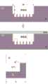
1.图1一种基于表面纳米气泡减阻的微通道制备过程示意图。其中,(a)为微通道的主通道;(b)为微通道底面的微孔结构;(c)为硅烷化出来后并用玻璃板密封后的微通道。1. Figure 1 is a schematic diagram of the preparation process of a microchannel based on surface nanobubble drag reduction. Among them, (a) is the main channel of the microchannel; (b) is the microporous structure of the bottom surface of the microchannel; (c) is the microchannel after silanization and sealing with a glass plate.
2.图2为一种基于表面纳米气泡减阻的微通道制备过程示意图中的基于表面纳米气泡减阻的微通道示意图。2. Figure 2 is a schematic diagram of a microchannel based on surface nanobubble drag reduction in the schematic diagram of the preparation process of a microchannel based on surface nanobubble drag reduction.
具体实施方式Detailed ways
下面将结合本发明实施例中的附图,对本发明实施例中的技术方案进行清楚、完整地描述,显然,所描述的实施例仅仅是本发明一部分实施例,而不是全部的实施例。基于本发明中的实施例,本领域普通技术人员在没有做出创造性劳动前提下所获得的所有其他实施例,都属于本发明保护的范围。The following will clearly and completely describe the technical solutions in the embodiments of the present invention with reference to the accompanying drawings in the embodiments of the present invention. Obviously, the described embodiments are only some, not all, embodiments of the present invention. Based on the embodiments of the present invention, all other embodiments obtained by persons of ordinary skill in the art without making creative efforts belong to the protection scope of the present invention.
请参阅图1和图2,本发明实施例中,首先采用RCA清洗工艺将硅片清洗干净,随后采用光刻技术(Photolithography)和电化学刻蚀技术(Electrochemical etching)的方法(硅片的加工面采用刻蚀液刻蚀,底面利用长波长的红外光照射)在硅表面上加工出宽度W=200μm、深度H=50μm的微通道主通道;加工时,所采用的刻蚀液为氢氟酸溶液(Hydrofluoric,HF);然后仍然利用同样的技术在通道底面上获得孔的直径为1.6μm、孔深为3μm的孔状微结构;接下来对底面带有微孔结构的微通道表面进行清洗(RCA工艺),用氮气吹干,利用体积比为1%OTS的无水甲苯溶液进行硅烷化处理;最后将玻璃片覆盖在微通道的上面并利用阳极焊技术密封。该方法具有较好的刻蚀效果,所加工的微通道可以通过改变微通道进出口的压力在微孔结构上诱捕到纳米气泡,实现利用纳米气泡降低流体流动阻力的应用。Please refer to Fig. 1 and Fig. 2, in the embodiment of the present invention, the silicon wafer is cleaned by RCA cleaning process at first, and then photolithography (Photolithography) and electrochemical etching (Electrochemical etching) methods (silicon wafer processing) are used to clean the silicon wafer. The main channel of the microchannel with width W=200μm and depth H=50μm is processed on the silicon surface; the etching solution used is hydrogen fluorine Acid solution (Hydrofluoric, HF); then still use the same technology to obtain a hole-like microstructure with a diameter of 1.6 μm and a hole depth of 3 μm on the bottom surface of the channel; Cleaning (RCA process), drying with nitrogen, and silanization with anhydrous toluene solution with a volume ratio of 1% OTS; finally, a glass sheet is covered on the microchannel and sealed using anodic welding technology. The method has a good etching effect, and the processed microchannel can trap nano-bubbles on the micropore structure by changing the pressure at the inlet and outlet of the micro-channel, so as to realize the application of reducing fluid flow resistance by using the nano-bubbles.
对于本领域技术人员而言,显然本发明不限于上述示范性实施例的细节,而且在不背离本发明的精神或基本特征的情况下,能够以其他的具体形式实现本发明。因此,无论从哪一点来看,均应将实施例看作是示范性的,而且是非限制性的,本发明的范围由所附权利要求而不是上述说明限定,因此旨在将落在权利要求的等同要件的含义和范围内的所有变化囊括在本发明内。不应将权利要求中的任何附图标记视为限制所涉及的权利要求。It will be apparent to those skilled in the art that the invention is not limited to the details of the above-described exemplary embodiments, but that the invention can be embodied in other specific forms without departing from the spirit or essential characteristics of the invention. Accordingly, the embodiments should be regarded in all points of view as exemplary and not restrictive, the scope of the invention being defined by the appended claims rather than the foregoing description, and it is therefore intended that the scope of the invention be defined by the appended claims rather than by the foregoing description. All changes within the meaning and range of equivalents of the elements are embraced in the present invention. Any reference sign in a claim should not be construed as limiting the claim concerned.
此外,应当理解,虽然本说明书按照实施方式加以描述,但并非每个实施方式仅包含一个独立的技术方案,说明书的这种叙述方式仅仅是为清楚起见,本领域技术人员应当将说明书作为一个整体,各实施例中的技术方案也可以经适当组合,形成本领域技术人员可以理解的其他实施方式。In addition, it should be understood that although this specification is described according to implementation modes, not each implementation mode only contains an independent technical solution, and this description in the specification is only for clarity, and those skilled in the art should take the specification as a whole , the technical solutions in the various embodiments can also be properly combined to form other implementations that can be understood by those skilled in the art.
Claims (2)
Priority Applications (1)
| Application Number | Priority Date | Filing Date | Title |
|---|---|---|---|
| CN201710229403.7ACN106861781B (en) | 2017-04-10 | 2017-04-10 | Micro-channel preparation method for reducing fluid resistance based on surface nano-bubbles |
Applications Claiming Priority (1)
| Application Number | Priority Date | Filing Date | Title |
|---|---|---|---|
| CN201710229403.7ACN106861781B (en) | 2017-04-10 | 2017-04-10 | Micro-channel preparation method for reducing fluid resistance based on surface nano-bubbles |
Publications (2)
| Publication Number | Publication Date |
|---|---|
| CN106861781A CN106861781A (en) | 2017-06-20 |
| CN106861781Btrue CN106861781B (en) | 2023-04-11 |
Family
ID=59162126
Family Applications (1)
| Application Number | Title | Priority Date | Filing Date |
|---|---|---|---|
| CN201710229403.7AExpired - Fee RelatedCN106861781B (en) | 2017-04-10 | 2017-04-10 | Micro-channel preparation method for reducing fluid resistance based on surface nano-bubbles |
Country Status (1)
| Country | Link |
|---|---|
| CN (1) | CN106861781B (en) |
Families Citing this family (3)
| Publication number | Priority date | Publication date | Assignee | Title |
|---|---|---|---|---|
| CN111282604B (en)* | 2020-02-12 | 2022-01-04 | 赛纳生物科技(北京)有限公司 | A biochemical chip microsphere entry method |
| EP4554780A2 (en)* | 2022-07-11 | 2025-05-21 | The Trustees of The University of Pennsylvania | Very large scale microfluidic integrated chip with micro-patterned wettability for high throughput multiple droplet generation |
| CN116060148B (en)* | 2023-02-17 | 2024-06-07 | 西南石油大学 | A method for in-situ controllable hydrophobic modification of nanochannels |
Citations (7)
| Publication number | Priority date | Publication date | Assignee | Title |
|---|---|---|---|---|
| US6303254B1 (en)* | 2000-10-20 | 2001-10-16 | Xerox Corporation | Electrostatographic imaging member |
| JP2006341154A (en)* | 2005-06-07 | 2006-12-21 | Kobe Steel Ltd | Micro fluid device and its manufacturing method |
| CN101613075A (en)* | 2009-07-28 | 2009-12-30 | 西安交通大学 | A Construction Method of Virtual Channel Constraining Droplet Movement |
| CN102481571A (en)* | 2009-06-16 | 2012-05-30 | 莱顿大学 | A Biological Microfluidics Chip And Related Methods |
| CN103638853A (en)* | 2013-11-11 | 2014-03-19 | 江苏大学 | S-type passive micro-mixer |
| CN105992648A (en)* | 2013-05-31 | 2016-10-05 | 彼克斯赛尔医疗科技有限公司 | Cartridge for preparing a sample fluid containing cells for analysis |
| CN207287463U (en)* | 2017-04-10 | 2018-05-01 | 黑龙江科技大学 | A kind of microchannel that fluid flow resistance is reduced based on nano surface bubble |
Family Cites Families (3)
| Publication number | Priority date | Publication date | Assignee | Title |
|---|---|---|---|---|
| EP1817576A1 (en)* | 2004-11-12 | 2007-08-15 | DiagnoSwiss S.A. | Microfluidic device with minimised ohmic resistance |
| BRPI0606335A2 (en)* | 2005-03-23 | 2009-09-29 | Velocys Inc | surface features in microprocessor technology |
| US9803239B2 (en)* | 2012-03-29 | 2017-10-31 | Complete Genomics, Inc. | Flow cells for high density array chips |
- 2017
- 2017-04-10CNCN201710229403.7Apatent/CN106861781B/ennot_activeExpired - Fee Related
Patent Citations (7)
| Publication number | Priority date | Publication date | Assignee | Title |
|---|---|---|---|---|
| US6303254B1 (en)* | 2000-10-20 | 2001-10-16 | Xerox Corporation | Electrostatographic imaging member |
| JP2006341154A (en)* | 2005-06-07 | 2006-12-21 | Kobe Steel Ltd | Micro fluid device and its manufacturing method |
| CN102481571A (en)* | 2009-06-16 | 2012-05-30 | 莱顿大学 | A Biological Microfluidics Chip And Related Methods |
| CN101613075A (en)* | 2009-07-28 | 2009-12-30 | 西安交通大学 | A Construction Method of Virtual Channel Constraining Droplet Movement |
| CN105992648A (en)* | 2013-05-31 | 2016-10-05 | 彼克斯赛尔医疗科技有限公司 | Cartridge for preparing a sample fluid containing cells for analysis |
| CN103638853A (en)* | 2013-11-11 | 2014-03-19 | 江苏大学 | S-type passive micro-mixer |
| CN207287463U (en)* | 2017-04-10 | 2018-05-01 | 黑龙江科技大学 | A kind of microchannel that fluid flow resistance is reduced based on nano surface bubble |
Non-Patent Citations (2)
| Title |
|---|
| Control of slippage with tunable bubble mattresses;Karatay E;《PNAS》;20130521* |
| 李成波.RCA.《光伏技术理论与应用》.2016,* |
Also Published As
| Publication number | Publication date |
|---|---|
| CN106861781A (en) | 2017-06-20 |
Similar Documents
| Publication | Publication Date | Title |
|---|---|---|
| CN106861781B (en) | Micro-channel preparation method for reducing fluid resistance based on surface nano-bubbles | |
| Iliescu et al. | Strategies in deep wet etching of Pyrex glass | |
| Wang et al. | Controlling flow behavior of water in microfluidics with a chemically patterned anisotropic wetting surface | |
| Zhang et al. | Ultrastable super-hydrophobic surface with an ordered scaly structure for decompression and guiding liquid manipulation | |
| CN103122311B (en) | Flexible three-dimensional single-cell targeted cultivating chip and controllable preparation method thereof | |
| Wang et al. | Morphology-patterned anisotropic wetting surface for fluid control and gas–liquid separation in microfluidics | |
| CN112744783B (en) | A method for preparing a super-hydrophobic and super-oleophobic surface of a micro-nano composite structure | |
| Chen et al. | A rapid and low-cost procedure for fabrication of glass microfluidic devices | |
| CN104998702A (en) | Preparation method of PDMS microfluidic chip based on liquid composite molding method | |
| CN106345543B (en) | A kind of microring array chip of the charge inducing electric osmose based on fixed potential | |
| CN103157525B (en) | Preparation method of microfluidic one-way valve device based on silicon nanopillar array | |
| CN207287463U (en) | A kind of microchannel that fluid flow resistance is reduced based on nano surface bubble | |
| CN107021449A (en) | Prepare the preparation method and applications at ordered micro-configuration and controllable chemical composition interface | |
| CN103333802A (en) | Inverted-cone array three-dimensional cell positioning cultivating chip and preparation method thereof | |
| CN101239285A (en) | A passive microfluidic mixer and packaging method thereof | |
| CN102627256A (en) | Micro-nano integrated processing technology based three-dimensional anti-drag micro-channel structure and preparation method thereof | |
| Wang et al. | Colloidal lithography-based fabrication of highly-ordered nanofluidic channels with an ultra-high surface-to-volume ratio | |
| CN116060148A (en) | A method for in-situ controllable hydrophobic modification of nanochannels | |
| CN112280083A (en) | Preparation method and application of bionic pitcher plant two-dimensional functional material | |
| US7523608B2 (en) | Electrically driven microfluidic pumping for actuation | |
| CN112473756A (en) | Method for processing PDMS micro-fluidic chip | |
| Kim et al. | Advancing liquid front shape control in capillary filling of microchannel via arrangement of microposts for microfluidic biomedical Sensors | |
| Choi et al. | Efficient microfluidic power generator based on interaction between DI water and hydrophobic-channel surface | |
| Kuo et al. | Capillary-driven dynamics of water in hydrophilic microscope coverslip nanochannels | |
| CN111569963B (en) | Horizontal nano-channel array, micro-nano fluidic chip and manufacturing method thereof |
Legal Events
| Date | Code | Title | Description |
|---|---|---|---|
| PB01 | Publication | ||
| PB01 | Publication | ||
| SE01 | Entry into force of request for substantive examination | ||
| SE01 | Entry into force of request for substantive examination | ||
| GR01 | Patent grant | ||
| GR01 | Patent grant | ||
| CF01 | Termination of patent right due to non-payment of annual fee | Granted publication date:20230411 | |
| CF01 | Termination of patent right due to non-payment of annual fee |