CN106847910B - A kind of GaN-based semiconductor device and preparation method thereof - Google Patents
A kind of GaN-based semiconductor device and preparation method thereofDownload PDFInfo
- Publication number
- CN106847910B CN106847910BCN201710139161.2ACN201710139161ACN106847910BCN 106847910 BCN106847910 BCN 106847910BCN 201710139161 ACN201710139161 ACN 201710139161ACN 106847910 BCN106847910 BCN 106847910B
- Authority
- CN
- China
- Prior art keywords
- layer
- gan
- algan barrier
- barrier layer
- multilayer
- Prior art date
- Legal status (The legal status is an assumption and is not a legal conclusion. Google has not performed a legal analysis and makes no representation as to the accuracy of the status listed.)
- Active
Links
Images


Classifications
- H—ELECTRICITY
- H10—SEMICONDUCTOR DEVICES; ELECTRIC SOLID-STATE DEVICES NOT OTHERWISE PROVIDED FOR
- H10D—INORGANIC ELECTRIC SEMICONDUCTOR DEVICES
- H10D30/00—Field-effect transistors [FET]
- H10D30/40—FETs having zero-dimensional [0D], one-dimensional [1D] or two-dimensional [2D] charge carrier gas channels
- H10D30/47—FETs having zero-dimensional [0D], one-dimensional [1D] or two-dimensional [2D] charge carrier gas channels having 2D charge carrier gas channels, e.g. nanoribbon FETs or high electron mobility transistors [HEMT]
- H10D30/471—High electron mobility transistors [HEMT] or high hole mobility transistors [HHMT]
- H10D30/475—High electron mobility transistors [HEMT] or high hole mobility transistors [HHMT] having wider bandgap layer formed on top of lower bandgap active layer, e.g. undoped barrier HEMTs such as i-AlGaN/GaN HEMTs
- H—ELECTRICITY
- H10—SEMICONDUCTOR DEVICES; ELECTRIC SOLID-STATE DEVICES NOT OTHERWISE PROVIDED FOR
- H10D—INORGANIC ELECTRIC SEMICONDUCTOR DEVICES
- H10D30/00—Field-effect transistors [FET]
- H10D30/01—Manufacture or treatment
- H10D30/015—Manufacture or treatment of FETs having heterojunction interface channels or heterojunction gate electrodes, e.g. HEMT
Landscapes
- Insulated Gate Type Field-Effect Transistor (AREA)
- Thin Film Transistor (AREA)
Abstract
Description
Translated fromChinese技术领域technical field
本发明属于半导体器件技术领域,具体涉及一种面向四维集成的GaN基纳米线晶体管及其制备方法。The invention belongs to the technical field of semiconductor devices, in particular to a four-dimensional integration-oriented GaN-based nanowire transistor and a preparation method thereof.
背景技术Background technique
作为传统硅基功率器件的替代品,基于第三代宽禁带半导体GaN材料的功率器件因其优异的材料特性和器件结构备受瞩目,GaN材料拥有较大的禁带宽度和电子迁移率,较好的热稳定性和化学稳定性,因而在大功率和高频领域有着广泛的应用前景而受到关注和研究。As a substitute for traditional silicon-based power devices, power devices based on the third-generation wide-bandgap semiconductor GaN materials have attracted much attention due to their excellent material properties and device structures. GaN materials have large band gaps and electron mobility. It has good thermal stability and chemical stability, so it has a wide range of application prospects in high-power and high-frequency fields and has attracted attention and research.
发明内容SUMMARY OF THE INVENTION
本发明的目的在于提供一种面向四维集成的GaN基半导体器件及其制备方法。这种垂直堆栈集成的功率器件表现出高的驱动电流,同时也满足集成电路进一步微缩化的需求。The purpose of the present invention is to provide a four-dimensional integration-oriented GaN-based semiconductor device and a preparation method thereof. This vertically stacked integrated power device exhibits high drive current while also meeting the demands of further miniaturization of integrated circuits.
本发明提供的GaN基半导体器件,包括:The GaN-based semiconductor device provided by the present invention includes:
绝缘GaN衬底;Insulating GaN substrate;
多层AlGaN势垒层/GaN层异质结叠层,位于所述GaN衬底上,包括相互隔离的源区和漏区两部分,其中,底层AlGaN势垒层未掺杂,其余各AlGaN势垒层和GaN层均掺杂;A multi-layer AlGaN barrier layer/GaN layer heterojunction stack, located on the GaN substrate, includes two parts of a source region and a drain region isolated from each other, wherein the underlying AlGaN barrier layer is not doped, and the remaining AlGaN potentials Both the barrier layer and the GaN layer are doped;
多层GaN纳米线沟道,分别与所述源区和漏区中相对应的GaN层相连接,且彼此隔离;multi-layer GaN nanowire channels, respectively connected with the corresponding GaN layers in the source region and the drain region, and isolated from each other;
栅极叠层,包括金属栅层和栅介质层,其中所述栅介质层覆盖所述GaN纳米线沟道,所述金属栅层位于所述栅介质层上;a gate stack, comprising a metal gate layer and a gate dielectric layer, wherein the gate dielectric layer covers the GaN nanowire channel, and the metal gate layer is located on the gate dielectric layer;
顶栅电极,位于所述金属栅层上;以及a top gate electrode on the metal gate layer; and
源电极、漏电极,分别位于所述源区和漏区的顶层GaN层上。The source electrode and the drain electrode are respectively located on the top GaN layer of the source region and the drain region.
优选的,所述GaN层的厚度为25-35纳米,更优选30纳米,所述AlGaN层的厚度为15-25纳米,更优选20纳米。Preferably, the thickness of the GaN layer is 25-35 nm, more preferably 30 nm, and the thickness of the AlGaN layer is 15-25 nm, more preferably 20 nm.
优选的,所述栅介质层为Al2O3,所述金属栅层为WN。Preferably, the gate dielectric layer is Al2 O3 , and the metal gate layer is WN.
优选的,所述Al2O3的厚度为8-15纳米,更优选10纳米,所述WN的厚度为35-45纳米,更优选40纳米。Preferably, the thickness of the Al2 O3 is 8-15 nm, more preferably 10 nm, and the thickness of the WN is 35-45 nm, more preferably 40 nm.
根据发明的另一方面,还公开一种GaN基半导体器件的制备方法,包括以下步骤:According to another aspect of the invention, a preparation method of a GaN-based semiconductor device is also disclosed, comprising the following steps:
提供绝缘GaN衬底;Provide insulating GaN substrate;
在所述GaN衬底上依次形成AlGaN势垒层和GaN层,重复多次,以形成多层AlGaN势垒层/GaN层异质结叠层;forming an AlGaN barrier layer and a GaN layer in sequence on the GaN substrate, repeating multiple times, to form a multi-layer AlGaN barrier layer/GaN layer heterojunction stack;
将所述多层AlGaN势垒层/GaN层异质结叠层分隔为源区和漏区,并进行源漏区注入,对除底层AlGaN势垒层外的各层进行掺杂;The multi-layer AlGaN barrier layer/GaN layer heterojunction stack is separated into a source region and a drain region, and the source and drain regions are implanted, and each layer except the underlying AlGaN barrier layer is doped;
对所述多层AlGaN势垒层/GaN层异质结叠层进行刻蚀,得到分别连接源区和漏区中对应的GaN层并且相互隔离的多层GaN纳米线沟道结构;Etching the multi-layer AlGaN barrier layer/GaN layer heterojunction stack to obtain a multi-layer GaN nanowire channel structure that connects the corresponding GaN layers in the source region and the drain region respectively and is isolated from each other;
在所述多层GaN纳米线沟道结构上形成栅介质层及金属栅层;forming a gate dielectric layer and a metal gate layer on the multi-layer GaN nanowire channel structure;
在所述金属栅层上形成顶栅电极;forming a top gate electrode on the metal gate layer;
分别在所述源区和漏区的顶层GaN层上形成源电极、漏电极。A source electrode and a drain electrode are formed on the top GaN layer of the source region and the drain region, respectively.
优选的,所述GaN层的厚度为25-35纳米,更优选30纳米,所述AlGaN层的厚度为15-25纳米,更优选20纳米。Preferably, the thickness of the GaN layer is 25-35 nm, more preferably 30 nm, and the thickness of the AlGaN layer is 15-25 nm, more preferably 20 nm.
优选的,所述栅介质层和所述金属栅层的形成方法为原子层沉积法。Preferably, the method for forming the gate dielectric layer and the metal gate layer is atomic layer deposition.
优选的,所述栅介质层为Al2O3,所述金属栅层为WN。Preferably, the gate dielectric layer is Al2 O3 , and the metal gate layer is WN.
优选的,所述Al2O3的厚度为8-15纳米,更优选10纳米,所述WN的厚度为35-45纳米,更优选40纳米。Preferably, the thickness of the Al2 O3 is 8-15 nm, more preferably 10 nm, and the thickness of the WN is 35-45 nm, more preferably 40 nm.
优选的,所述源漏区注入采用硅掺杂。Preferably, the source and drain regions are implanted with silicon doping.
本发明提供的新型GaN基纳米线晶体管在保证关态电流不衰减的前提下,表现出高的驱动电流。因此,能够很好地应用于低功耗逻辑以及射频领域。The novel GaN-based nanowire transistor provided by the present invention exhibits high driving current on the premise of ensuring that the off-state current does not decay. Therefore, it can be well applied to low-power logic and radio frequency fields.
附图说明Description of drawings
图1 是GaN基半导体器件制备方法的流程图。FIG. 1 is a flow chart of a method for fabricating a GaN-based semiconductor device.
图2是形成底层AlGaN势垒层后的器件结构示意图。FIG. 2 is a schematic diagram of the device structure after forming the underlying AlGaN barrier layer.
图3是形成三层AlGaN势垒层/GaN层异质结叠层结构后的器件结构示意图。FIG. 3 is a schematic diagram of the device structure after forming a three-layer AlGaN barrier layer/GaN layer heterojunction stack structure.
图4是形成源、漏区后的器件结构示意图。FIG. 4 is a schematic diagram of the structure of the device after the source and drain regions are formed.
图5是沉积Al2O3层后的器件结构示意图。FIG. 5 is a schematic diagram of the device structure after depositing an Al2 O3 layer.
图6是形成Al2O3掩膜层后的器件结构示意图。FIG. 6 is a schematic diagram of the device structure after forming the Al2 O3 mask layer.
图7是刻蚀形成鳍片结构后的器件结构示意图。FIG. 7 is a schematic diagram of a device structure after etching to form a fin structure.
图8是形成三层GaN纳米线沟道结构后的器件结构示意图。FIG. 8 is a schematic diagram of the device structure after the three-layer GaN nanowire channel structure is formed.
图9是形成栅介质层和金属栅层后的器件结构示意图。FIG. 9 is a schematic diagram of the device structure after forming a gate dielectric layer and a metal gate layer.
图10是图9沿A-A'的剖面结构示意图。FIG. 10 is a schematic view of the cross-sectional structure of FIG. 9 along A-A'.
图11是形成顶栅电极后的器件结构示意图。FIG. 11 is a schematic diagram of the device structure after the top gate electrode is formed.
图12是GaN基半导体器件的结构示意图。FIG. 12 is a schematic structural diagram of a GaN-based semiconductor device.
具体实施方式Detailed ways
为了使本发明的目的、技术方案及优点更加清楚明白,下面将结合本发明实施例中的附图,对本发明实施例中的技术方案进行清楚、完整地描述,应当理解,此处所描述的具体实施例仅用以解释本发明,并不用于限定本发明。所描述的实施例仅仅是本发明一部分实施例,而不是全部的实施例。基于本发明中的实施例,本领域普通技术人员在没有做出创造性劳动前提下所获得的所有其它实施例,都属于本发明保护的范围。In order to make the objectives, technical solutions and advantages of the present invention clearer, the technical solutions in the embodiments of the present invention will be clearly and completely described below with reference to the accompanying drawings in the embodiments of the present invention. It should be understood that the specific The embodiments are only used to explain the present invention, and are not intended to limit the present invention. The described embodiments are only some, but not all, embodiments of the present invention. Based on the embodiments of the present invention, all other embodiments obtained by those of ordinary skill in the art without creative efforts shall fall within the protection scope of the present invention.
图1是GaN基半导体器件的制备流程图。图2~图12是GaN基半导体器件制备过程中各阶段的器件结构示意图。以下结合图1~图12对GaN基半导体器件的制备方法的具体实施例进行说明。本实施方式中,以三层垂直堆栈集成的GaN基纳米线晶体管阵列为例,但是本发明不限定于此,也可是两层、四层等其他任意多层的结构。FIG. 1 is a flow chart of the fabrication of a GaN-based semiconductor device. 2 to 12 are schematic diagrams of device structures at various stages in the fabrication process of a GaN-based semiconductor device. Specific embodiments of the manufacturing method of the GaN-based semiconductor device will be described below with reference to FIGS. 1 to 12 . In this embodiment, a three-layer vertically stacked GaN-based nanowire transistor array is used as an example, but the present invention is not limited to this, and other arbitrary multi-layer structures such as two-layer and four-layer are also possible.
首先,在步骤S1中,提供绝缘GaN衬底100。例如,厚度为300微米、直径为2英吋。First, in step S1, an
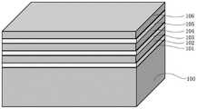
接下来,在步骤S2中,采用金属有机化学气相沉积方法(MOCVD)在GaN衬底100上外延形成AlGaN势垒层101,厚度优选为20纳米,所得结构如图2所示。之后,采用MOCVD法外延GaN层102,其厚度优选为30纳米。重复步骤S2,直至形成三层AlGaN势垒层/GaN层异质结叠层结构,如图3所示,包括AlGaN势垒层101、GaN层102、AlGaN势垒层103、GaN层104、AlGaN势垒层105和GaN层106。Next, in step S2 , an AlGaN
接下来,在步骤S3中,对上述三层AlGaN势垒层/GaN层异质结叠层结构进行分区,形成源区和漏区。具体步骤如下:首先采用化学气相沉积(CVD)法淀积约100纳米的Si3N4作为掩膜,进行光刻,形成源、漏区域窗口。然后,对源、漏区域进行硅注入,也即对除底层AlGaN势垒层101外的各层(GaN层102、AlGaN势垒层103、GaN层104、AlGaN势垒层105和GaN层106)进行掺杂并且在氮气氛围内活化退火形成源、漏接触。最后,选取CF4作为刻蚀气体,反应离子刻蚀Si3N4掩膜。在图4中示出了形成源、漏区后的器件结构示意图。如图4所示,三层AlGaN势垒层/GaN层异质结叠层被分隔为源区2和漏区3,其中,位于源区的三层AlGaN势垒层/GaN层异质结叠层包括AlGaN势垒层101、GaN层202、AlGaN势垒层203、GaN层204、AlGaN势垒层205和GaN层206,位于漏区的三层AlGaN势垒层/GaN层异质结叠层包括AlGaN势垒层101、GaN层302、AlGaN势垒层303、GaN层304、AlGaN势垒层305和GaN层306。Next, in step S3, the above-mentioned three-layer AlGaN barrier layer/GaN layer heterojunction stack structure is partitioned to form a source region and a drain region. The specific steps are as follows: first, a chemical vapor deposition (CVD) method is used to deposit Si3 N4 with a thickness of about 100 nanometers as a mask, and photolithography is performed to form the source and drain area windows. Then, silicon implantation is performed on the source and drain regions, that is, on the layers except the underlying AlGaN barrier layer 101 (
接下来,在步骤S4中,对三层AlGaN势垒层/GaN层异质结叠层进行刻蚀,得到三层GaN纳米线沟道结构,其分别连接源区2和漏区3中相对应的GaN层,并且GaN纳米线沟道彼此相互隔离。具体步骤如下:首先,采用原子层沉积(ALD)法淀积约10纳米厚的Al2O3层107,所得结构如图5所示;之后,悬涂电子束正胶,曝光出鳍片(Fin)结构的图形,反应离子刻蚀曝露出的Al2O3层107,得到Al2O3硬掩膜结构108,所得结构如图6所示。之后,以BCl3作为刻蚀气体,刻蚀得到Fin结构,所得结构如图7所示,包括GaN层402、AlGaN势垒层403、GaN层404、AlGaN势垒层405和GaN层406。最后,将上述器件结构放入稀释的HCl溶液,去除顶部Al2O3硬掩膜结构108以及鳍片结构中的AlGaN势垒层403和405,得到三层GaN纳米线沟道结构,也即GaN层402、404和406,所得结构如图8所示。Next, in step S4, the three-layer AlGaN barrier layer/GaN layer heterojunction stack is etched to obtain a three-layer GaN nanowire channel structure, which is connected to the
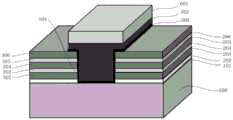
接下来,在步骤S5中,在三层GaN纳米线沟道结构上外延栅介质层及金属栅层。具体而言,首先,采用原子层沉积法沉积10纳米的Al2O3作为栅介质层501。 然后,采用原子层沉积法沉积40纳米的WN作为金属栅层502,所得结构如图9所示。 为了更清楚的展示器件结构,在图10中示出了所形成的器件的剖面结构示意图。如图10所示,所形成的栅介质层501覆盖三层GaN纳米线沟道结构也即GaN层402、404和406,金属栅层502位于栅介质层501上,将其包覆。Next, in step S5, a gate dielectric layer and a metal gate layer are epitaxially formed on the three-layer GaN nanowire channel structure. Specifically, first, Al2 O3 of 10 nm is deposited as the
接下来,在步骤S6中,在金属栅层502上形成顶栅电极601,所得结构如图11所示。例如,采用物理气相沉积(PVD)法淀积Ni/Au顶栅金属,而后悬涂光刻胶并进行刻蚀,去除多余的Ni/Au金属层以及WN层,得到顶栅电极601。Next, in step S6, a
最后,在步骤S7中,分别在源区2和漏区3的顶层GaN层206和306上形成源电极602、漏电极603。具体而言,例如采用PVD法淀积Ti/Al/Ni/Au金属,然后悬涂光刻胶并进行刻蚀,去除多余的Ti/Al/Ni/Au金属,得到源电极602和漏电极603,所得结构如图12所示。Finally, in step S7, a
本发明还提供一种GaN基半导体器件。在图12中示出了GaN基半导体器件的立体结构示意图。如图1所示,GaN基半导体器件包括:绝缘GaN衬底100,例如厚度为300微米、直径为2英吋的GaN衬底。The present invention also provides a GaN-based semiconductor device. A schematic three-dimensional structure of a GaN-based semiconductor device is shown in FIG. 12 . As shown in FIG. 1, the GaN-based semiconductor device includes: an insulating
三层AlGaN势垒层/GaN层异质结叠层,位于GaN衬底100上,包括相互隔离的源区和漏区两部分,其中,位于源区的三层AlGaN势垒层/GaN层异质结叠层包括AlGaN势垒层101、GaN层202、AlGaN势垒层203、GaN层204、AlGaN势垒层205和GaN层206,位于漏区的三层AlGaN势垒层/GaN层异质结叠层包括AlGaN势垒层101、GaN层302、AlGaN势垒层303、GaN层304、AlGaN势垒层305和GaN层306;除位于GaN衬底100上的底层AlGaN势垒层101未掺杂外,其余各GaN层和AlGaN势垒层均掺杂。优选采用硅注入掺杂。GaN层的厚度为30纳米,AlGaN势垒层的厚度为20纳米。A three-layer AlGaN barrier layer/GaN layer heterojunction stack, located on the
三层GaN纳米线沟道,分别与三层AlGaN势垒层/GaN层异质结叠层中的对应的掺杂GaN层相连接,且彼此间保持一定间距,相互隔离,具体结构参见图8。栅极叠层,包括金属栅层502和栅介质层501,其中栅介质层501覆盖三层GaN纳米线沟道,金属栅层502位于栅介质层501上,具体结构参见图9和图10。栅介质层例如为Al2O3,金属栅层例如为WN。顶栅电极601,位于金属栅层502上,例如为Ni/Au金属。源电极602和漏电极603,分别位于源区的GaN层206和漏区的GaN层306上。优选采用Ti/Al/Ni/Au金属。The three-layer GaN nanowire channels are respectively connected with the corresponding doped GaN layers in the three-layer AlGaN barrier layer/GaN layer heterojunction stack, and keep a certain distance from each other and are isolated from each other. The specific structure is shown in Figure 8 . The gate stack includes a
本发明的GaN基半导体器件制备在GaN基片上,摒弃了常规的横向堆栈集成结构,采用四维垂直堆栈集成,集成度极大提升,满足半导体器件尺寸日益微缩化的需求。在器件性能上,这种新型GaN基纳米线晶体管在保证关态电流不衰减的前提下,表现出高的驱动电流。因此,能够很好地应用于低功耗逻辑以及射频领域。The GaN-based semiconductor device of the present invention is prepared on a GaN substrate, abandons the conventional horizontal stack integration structure, adopts four-dimensional vertical stack integration, greatly improves the integration degree, and satisfies the increasingly miniaturized size of the semiconductor device. In terms of device performance, this new type of GaN-based nanowire transistor exhibits high drive current on the premise of ensuring that the off-state current does not decay. Therefore, it can be well applied to low-power logic and radio frequency fields.
以上,针对本发明的GaN基半导体器件及其制备方法的具体实施方式进行了详细说明,但是本发明不限定于此。例如,部分步骤的顺序可以调换,部分步骤可以省略。另外,各步骤的具体实施方式根据情况可以不同。此外,外延方法、刻蚀的方法、器件各部分的材料、厚度等参数均可根据实际情况进行选择。The specific embodiments of the GaN-based semiconductor device and the manufacturing method thereof of the present invention have been described in detail above, but the present invention is not limited thereto. For example, the order of some steps may be reversed, and some steps may be omitted. In addition, the specific implementation of each step may vary according to circumstances. In addition, parameters such as epitaxy method, etching method, material and thickness of each part of the device can be selected according to the actual situation.
以上所述,仅为本发明的具体实施方式,但本发明的保护范围并不局限于此,任何熟悉本技术领域的技术人员在本发明揭露的技术范围内,可轻易想到的变化或替换,都应涵盖在本发明的保护范围之内。The above are only specific embodiments of the present invention, but the protection scope of the present invention is not limited thereto. Any person skilled in the art who is familiar with the technical scope disclosed by the present invention can easily think of changes or substitutions. All should be included within the protection scope of the present invention.
Claims (8)
Priority Applications (1)
| Application Number | Priority Date | Filing Date | Title |
|---|---|---|---|
| CN201710139161.2ACN106847910B (en) | 2017-03-09 | 2017-03-09 | A kind of GaN-based semiconductor device and preparation method thereof |
Applications Claiming Priority (1)
| Application Number | Priority Date | Filing Date | Title |
|---|---|---|---|
| CN201710139161.2ACN106847910B (en) | 2017-03-09 | 2017-03-09 | A kind of GaN-based semiconductor device and preparation method thereof |
Publications (2)
| Publication Number | Publication Date |
|---|---|
| CN106847910A CN106847910A (en) | 2017-06-13 |
| CN106847910Btrue CN106847910B (en) | 2020-07-07 |
Family
ID=59144095
Family Applications (1)
| Application Number | Title | Priority Date | Filing Date |
|---|---|---|---|
| CN201710139161.2AActiveCN106847910B (en) | 2017-03-09 | 2017-03-09 | A kind of GaN-based semiconductor device and preparation method thereof |
Country Status (1)
| Country | Link |
|---|---|
| CN (1) | CN106847910B (en) |
Families Citing this family (1)
| Publication number | Priority date | Publication date | Assignee | Title |
|---|---|---|---|---|
| CN112968053B (en)* | 2021-02-01 | 2022-09-09 | 深圳大学 | Field effect transistor and preparation method thereof |
Family Cites Families (4)
| Publication number | Priority date | Publication date | Assignee | Title |
|---|---|---|---|---|
| US9099388B2 (en)* | 2011-10-21 | 2015-08-04 | Taiwan Semiconductor Manufacturing Company, Ltd. | III-V multi-channel FinFETs |
| CN106887453B (en)* | 2011-12-19 | 2020-08-21 | 英特尔公司 | Group III-N Nanowire Transistors |
| CN102623384A (en)* | 2012-03-31 | 2012-08-01 | 上海华力微电子有限公司 | Fabrication Method of Gate-last Si-NWFET Based on SOI Vertical Stacking |
| US8823059B2 (en)* | 2012-09-27 | 2014-09-02 | Intel Corporation | Non-planar semiconductor device having group III-V material active region with multi-dielectric gate stack |
- 2017
- 2017-03-09CNCN201710139161.2Apatent/CN106847910B/enactiveActive
Non-Patent Citations (1)
| Title |
|---|
| 一种新型高速嵌入式动态随机存储器;藏松干等;《微电子学》;20120209;第42卷(第1期);第1-4页* |
Also Published As
| Publication number | Publication date |
|---|---|
| CN106847910A (en) | 2017-06-13 |
Similar Documents
| Publication | Publication Date | Title |
|---|---|---|
| JP5260550B2 (en) | Active region molding for group III nitride devices and method of manufacturing the same | |
| JP2008270794A (en) | Semiconductor device and manufacturing method thereof | |
| KR102805278B1 (en) | Two dimensional(2D) material based line conductive layer contact structure, electronic device including the same and method of manufacturing electronic device | |
| TWI725433B (en) | Manufacturing method of semiconductor device | |
| CN108461543A (en) | A kind of GaN HEMT devices and preparation method thereof | |
| CN106549031A (en) | A kind of monolithic integrated device based on body GaN material and preparation method thereof | |
| JP2014199864A (en) | Semiconductor device and method of manufacturing the same | |
| CN107887383A (en) | GaN-based monolithic power inverter and manufacturing method thereof | |
| CN116169169A (en) | Enhanced GaN HEMTs with low gate leakage current and its preparation method | |
| CN106252373B (en) | A GaN-based integrated device and its preparation method | |
| CN111223928A (en) | Gate finger gradually widened GaN FinFET structure and preparation method thereof | |
| CN111509042A (en) | A kind of MIS structure GaN high electron mobility transistor and preparation method thereof | |
| CN106847910B (en) | A kind of GaN-based semiconductor device and preparation method thereof | |
| CN112670342B (en) | High electron mobility transistor and preparation method thereof | |
| CN112420615B (en) | Semiconductor structure preparation method and semiconductor device | |
| CN105679679B (en) | A kind of preparation method of GaN base notched gates MISFET | |
| CN209766428U (en) | Novel MIS-HEMT device structure | |
| CN109888012B (en) | GaN-based super-junction vertical power transistor and manufacturing method thereof | |
| CN112768508A (en) | Back gate full-control AlGaN/GaN heterojunction enhanced power HEMT device and preparation method thereof | |
| CN108022925B (en) | GaN-based monolithic power converter and manufacturing method thereof | |
| CN114883407B (en) | HEMT based on Fin-FET gate structure and its fabrication method | |
| CN112838120B (en) | Ring-gate enhanced AlGaN/GaN power HEMT device and preparation method thereof | |
| TW201929221A (en) | Semiconductor device and the manufacture thereof | |
| CN209266410U (en) | Gate structure of GaN-based power devices | |
| CN108198758B (en) | A vertical structure gallium nitride power diode device and its manufacturing method |
Legal Events
| Date | Code | Title | Description |
|---|---|---|---|
| PB01 | Publication | ||
| PB01 | Publication | ||
| SE01 | Entry into force of request for substantive examination | ||
| SE01 | Entry into force of request for substantive examination | ||
| GR01 | Patent grant | ||
| GR01 | Patent grant |