CN106663640B - Method of providing electronic device and electronic device thereof - Google Patents
Method of providing electronic device and electronic device thereofDownload PDFInfo
- Publication number
- CN106663640B CN106663640BCN201580038025.3ACN201580038025ACN106663640BCN 106663640 BCN106663640 BCN 106663640BCN 201580038025 ACN201580038025 ACN 201580038025ACN 106663640 BCN106663640 BCN 106663640B
- Authority
- CN
- China
- Prior art keywords
- substrate
- adhesion
- carrier substrate
- device substrate
- modifying layer
- Prior art date
- Legal status (The legal status is an assumption and is not a legal conclusion. Google has not performed a legal analysis and makes no representation as to the accuracy of the status listed.)
- Active
Links
Images


Classifications
- H—ELECTRICITY
- H01—ELECTRIC ELEMENTS
- H01L—SEMICONDUCTOR DEVICES NOT COVERED BY CLASS H10
- H01L24/00—Arrangements for connecting or disconnecting semiconductor or solid-state bodies; Methods or apparatus related thereto
- H01L24/80—Methods for connecting semiconductor or other solid state bodies using means for bonding being attached to, or being formed on, the surface to be connected
- H01L24/83—Methods for connecting semiconductor or other solid state bodies using means for bonding being attached to, or being formed on, the surface to be connected using a layer connector
- H—ELECTRICITY
- H01—ELECTRIC ELEMENTS
- H01L—SEMICONDUCTOR DEVICES NOT COVERED BY CLASS H10
- H01L21/00—Processes or apparatus adapted for the manufacture or treatment of semiconductor or solid state devices or of parts thereof
- H01L21/67—Apparatus specially adapted for handling semiconductor or electric solid state devices during manufacture or treatment thereof; Apparatus specially adapted for handling wafers during manufacture or treatment of semiconductor or electric solid state devices or components ; Apparatus not specifically provided for elsewhere
- H01L21/683—Apparatus specially adapted for handling semiconductor or electric solid state devices during manufacture or treatment thereof; Apparatus specially adapted for handling wafers during manufacture or treatment of semiconductor or electric solid state devices or components ; Apparatus not specifically provided for elsewhere for supporting or gripping
- H01L21/6835—Apparatus specially adapted for handling semiconductor or electric solid state devices during manufacture or treatment thereof; Apparatus specially adapted for handling wafers during manufacture or treatment of semiconductor or electric solid state devices or components ; Apparatus not specifically provided for elsewhere for supporting or gripping using temporarily an auxiliary support
- H01L21/6836—Wafer tapes, e.g. grinding or dicing support tapes
- H—ELECTRICITY
- H01—ELECTRIC ELEMENTS
- H01L—SEMICONDUCTOR DEVICES NOT COVERED BY CLASS H10
- H01L24/00—Arrangements for connecting or disconnecting semiconductor or solid-state bodies; Methods or apparatus related thereto
- H01L24/01—Means for bonding being attached to, or being formed on, the surface to be connected, e.g. chip-to-package, die-attach, "first-level" interconnects; Manufacturing methods related thereto
- H01L24/26—Layer connectors, e.g. plate connectors, solder or adhesive layers; Manufacturing methods related thereto
- H01L24/28—Structure, shape, material or disposition of the layer connectors prior to the connecting process
- H01L24/29—Structure, shape, material or disposition of the layer connectors prior to the connecting process of an individual layer connector
- H—ELECTRICITY
- H01—ELECTRIC ELEMENTS
- H01L—SEMICONDUCTOR DEVICES NOT COVERED BY CLASS H10
- H01L2221/00—Processes or apparatus adapted for the manufacture or treatment of semiconductor or solid state devices or of parts thereof covered by H01L21/00
- H01L2221/67—Apparatus for handling semiconductor or electric solid state devices during manufacture or treatment thereof; Apparatus for handling wafers during manufacture or treatment of semiconductor or electric solid state devices or components; Apparatus not specifically provided for elsewhere
- H01L2221/683—Apparatus for handling semiconductor or electric solid state devices during manufacture or treatment thereof; Apparatus for handling wafers during manufacture or treatment of semiconductor or electric solid state devices or components; Apparatus not specifically provided for elsewhere for supporting or gripping
- H01L2221/68304—Apparatus for handling semiconductor or electric solid state devices during manufacture or treatment thereof; Apparatus for handling wafers during manufacture or treatment of semiconductor or electric solid state devices or components; Apparatus not specifically provided for elsewhere for supporting or gripping using temporarily an auxiliary support
- H01L2221/68318—Auxiliary support including means facilitating the separation of a device or wafer from the auxiliary support
- H—ELECTRICITY
- H01—ELECTRIC ELEMENTS
- H01L—SEMICONDUCTOR DEVICES NOT COVERED BY CLASS H10
- H01L2221/00—Processes or apparatus adapted for the manufacture or treatment of semiconductor or solid state devices or of parts thereof covered by H01L21/00
- H01L2221/67—Apparatus for handling semiconductor or electric solid state devices during manufacture or treatment thereof; Apparatus for handling wafers during manufacture or treatment of semiconductor or electric solid state devices or components; Apparatus not specifically provided for elsewhere
- H01L2221/683—Apparatus for handling semiconductor or electric solid state devices during manufacture or treatment thereof; Apparatus for handling wafers during manufacture or treatment of semiconductor or electric solid state devices or components; Apparatus not specifically provided for elsewhere for supporting or gripping
- H01L2221/68304—Apparatus for handling semiconductor or electric solid state devices during manufacture or treatment thereof; Apparatus for handling wafers during manufacture or treatment of semiconductor or electric solid state devices or components; Apparatus not specifically provided for elsewhere for supporting or gripping using temporarily an auxiliary support
- H01L2221/6835—Apparatus for handling semiconductor or electric solid state devices during manufacture or treatment thereof; Apparatus for handling wafers during manufacture or treatment of semiconductor or electric solid state devices or components; Apparatus not specifically provided for elsewhere for supporting or gripping using temporarily an auxiliary support used as a support during build up manufacturing of active devices
- H—ELECTRICITY
- H01—ELECTRIC ELEMENTS
- H01L—SEMICONDUCTOR DEVICES NOT COVERED BY CLASS H10
- H01L2221/00—Processes or apparatus adapted for the manufacture or treatment of semiconductor or solid state devices or of parts thereof covered by H01L21/00
- H01L2221/67—Apparatus for handling semiconductor or electric solid state devices during manufacture or treatment thereof; Apparatus for handling wafers during manufacture or treatment of semiconductor or electric solid state devices or components; Apparatus not specifically provided for elsewhere
- H01L2221/683—Apparatus for handling semiconductor or electric solid state devices during manufacture or treatment thereof; Apparatus for handling wafers during manufacture or treatment of semiconductor or electric solid state devices or components; Apparatus not specifically provided for elsewhere for supporting or gripping
- H01L2221/68304—Apparatus for handling semiconductor or electric solid state devices during manufacture or treatment thereof; Apparatus for handling wafers during manufacture or treatment of semiconductor or electric solid state devices or components; Apparatus not specifically provided for elsewhere for supporting or gripping using temporarily an auxiliary support
- H01L2221/68381—Details of chemical or physical process used for separating the auxiliary support from a device or wafer
- H—ELECTRICITY
- H01—ELECTRIC ELEMENTS
- H01L—SEMICONDUCTOR DEVICES NOT COVERED BY CLASS H10
- H01L2224/00—Indexing scheme for arrangements for connecting or disconnecting semiconductor or solid-state bodies and methods related thereto as covered by H01L24/00
- H01L2224/80—Methods for connecting semiconductor or other solid state bodies using means for bonding being attached to, or being formed on, the surface to be connected
- H01L2224/83—Methods for connecting semiconductor or other solid state bodies using means for bonding being attached to, or being formed on, the surface to be connected using a layer connector
- H01L2224/83053—Bonding environment
- H01L2224/8309—Vacuum
- H—ELECTRICITY
- H01—ELECTRIC ELEMENTS
- H01L—SEMICONDUCTOR DEVICES NOT COVERED BY CLASS H10
- H01L2224/00—Indexing scheme for arrangements for connecting or disconnecting semiconductor or solid-state bodies and methods related thereto as covered by H01L24/00
- H01L2224/80—Methods for connecting semiconductor or other solid state bodies using means for bonding being attached to, or being formed on, the surface to be connected
- H01L2224/83—Methods for connecting semiconductor or other solid state bodies using means for bonding being attached to, or being formed on, the surface to be connected using a layer connector
- H01L2224/8334—Bonding interfaces of the layer connector
- H01L2224/83359—Material
Landscapes
- Engineering & Computer Science (AREA)
- Computer Hardware Design (AREA)
- Power Engineering (AREA)
- Microelectronics & Electronic Packaging (AREA)
- General Physics & Mathematics (AREA)
- Manufacturing & Machinery (AREA)
- Physics & Mathematics (AREA)
- Condensed Matter Physics & Semiconductors (AREA)
- Thin Film Transistor (AREA)
- Laminated Bodies (AREA)
- Electric Connection Of Electric Components To Printed Circuits (AREA)
- Wire Bonding (AREA)
- Container, Conveyance, Adherence, Positioning, Of Wafer (AREA)
Abstract
Translated fromChinese
Description
Translated fromChinese关于由联邦政府赞助的研究或开发的声明Statement Regarding Federally Sponsored Research or Development
本发明是在陆军研究办公室授予的W911NF-04-2-0005下在政府支持下作出的。政府在本发明中具有某些权利。This invention was made with government support under W911NF-04-2-0005 awarded by the Army Research Office. The government has certain rights in this invention.
相关申请的交叉引用CROSS-REFERENCE TO RELATED APPLICATIONS
本申请要求2014年5月13日提交的美国临时专利申请号61/992,799的利益。美国临时专利申请号61/992,799通过引用以其全部结合于此。This application claims the benefit of US Provisional Patent Application No. 61/992,799, filed May 13, 2014. US Provisional Patent Application No. 61/992,799 is incorporated herein by reference in its entirety.
技术领域technical field
本发明总体上涉及制造电子器件,并且更具体地涉及制造在柔性衬底上具有一个或多个半导体元件的电子器件以及由此制造的电子器件。The present invention relates generally to the manufacture of electronic devices, and more particularly to the manufacture of electronic devices having one or more semiconductor elements on flexible substrates and electronic devices manufactured thereby.
背景技术Background technique
在电子设备行业中,柔性衬底作为用于电子器件的基底正在快速变得越来越受欢迎。柔性衬底可以包括多种多样的材料,比如像以下各项中的任一项:大量的塑料、金属箔和玻璃(例如,氟硅酸盐玻璃、硼硅玻璃、康宁(Corning)
在本领域中需要开发一种用于制造具有柔性衬底的电子器件的方法,该方法允许对电气特性进行改进,比如像对参数特性和/或使用寿命进行改进,并且允许减小弓弯、翘曲、和/或变形。There is a need in the art to develop a method for fabricating electronic devices with flexible substrates that allows improvements in electrical properties, such as parametric properties and/or lifetime, and allows for reduced bowing, Warping, and/or deformation.
附图说明Description of drawings
为方便进一步描述这些实施例,提供了如下附图,在附图中:In order to further describe these embodiments, the following drawings are provided, in which:
图1展示了提供半导体器件的方法的实施例的流程图;1 illustrates a flowchart of an embodiment of a method of providing a semiconductor device;
图2展示了根据图1的实施例的提供半导体器件的载体衬底的示例性活动;FIG. 2 illustrates an exemplary activity of providing a carrier substrate for a semiconductor device in accordance with the embodiment of FIG. 1;
图3展示了根据图1的实施例的在载体衬底的至少一部分上提供半导体器件的粘接改性层的示例性活动;3 illustrates exemplary activities for providing an adhesion-modifying layer of a semiconductor device on at least a portion of a carrier substrate in accordance with the embodiment of FIG. 1;
图4展示了根据实施例的在载体衬底上提供粘接改性层之后的半导体器件的局部横截面图;4 illustrates a partial cross-sectional view of a semiconductor device after providing an adhesion-modifying layer on a carrier substrate according to an embodiment;
图5展示了根据实施例的半导体器件的局部横截面图,其中,已经通过蚀刻移除了半导体器件的粘接改性层的中央部分,以便留下粘接改性层的周边部分并且暴露出载体衬底;5 illustrates a partial cross-sectional view of a semiconductor device in which a central portion of an adhesion-modifying layer of the semiconductor device has been removed by etching to leave a peripheral portion of the adhesion-modifying layer and expose carrier substrate;
图6展示了根据图4的实施例的在载体衬底上和粘接改性层上提供粘接剂之后的半导体器件的局部横截面图;6 illustrates a partial cross-sectional view of the semiconductor device after providing an adhesive on the carrier substrate and on the adhesion-modifying layer according to the embodiment of FIG. 4;
图7展示了根据图1的实施例的将器件衬底与载体衬底联接在一起的示例性活动;FIG. 7 illustrates an exemplary activity of coupling a device substrate and a carrier substrate together in accordance with the embodiment of FIG. 1;
图8展示了根据图7的实施例将器件衬底直接粘合到粘接改性层上的示例性活动;FIG. 8 illustrates an exemplary activity for directly adhering a device substrate to an adhesion-modifying layer according to the embodiment of FIG. 7;
图9展示了根据图5的实施例的在将器件衬底直接粘合到粘接改性层上并且粘合在载体衬底上之后的半导体器件的局部横截面图;9 illustrates a partial cross-sectional view of the semiconductor device after direct bonding of the device substrate to the adhesion modification layer and to the carrier substrate in accordance with the embodiment of FIG. 5;
图10展示了根据图7的实施例的通过粘接剂将器件衬底粘合到粘接改性层上的示例性活动;FIG. 10 illustrates an exemplary activity for bonding a device substrate to an adhesion-modifying layer with an adhesive in accordance with the embodiment of FIG. 7;
图11展示了根据图4的实施例在将器件衬底通过粘接剂粘合到粘接改性层上并且将其粘合在载体衬底上之后的半导体器件的局部横截面图;11 shows a partial cross-sectional view of the semiconductor device after bonding the device substrate with an adhesive to the adhesion-modifying layer and bonding it to the carrier substrate in accordance with the embodiment of FIG. 4;
图12展示了根据图4的实施例的在器件衬底上提供一个或多个半导体元件之后的半导体器件的局部横截面图;12 illustrates a partial cross-sectional view of a semiconductor device after providing one or more semiconductor elements on a device substrate in accordance with the embodiment of FIG. 4;
图13展示了根据图5的实施例的在器件衬底上提供一个或多个半导体元件之后的半导体器件的局部横截面图;13 illustrates a partial cross-sectional view of a semiconductor device after providing one or more semiconductor elements on a device substrate in accordance with the embodiment of FIG. 5;
图14展示了根据图5的实施例的在将器件衬底的器件部分与器件衬底的非器件部分切断之后的半导体器件的局部横截面图;14 illustrates a partial cross-sectional view of a semiconductor device after severing a device portion of the device substrate from a non-device portion of the device substrate in accordance with the embodiment of FIG. 5;
图15展示了根据图4的实施例的在将器件衬底与载体衬底分离之后的半导体器件的器件衬底的横截面图;15 illustrates a cross-sectional view of the device substrate of the semiconductor device after separation of the device substrate from the carrier substrate in accordance with the embodiment of FIG. 4;
图16展示了根据图5的实施例的在将器件部分与载体衬底分离之后的半导体器件的器件衬底的器件部分的横截面图;16 illustrates a cross-sectional view of a device portion of a device substrate of a semiconductor device after separation of the device portion from the carrier substrate in accordance with the embodiment of FIG. 5;
图17是通过傅里叶变换红外光谱法展示了根据将聚萘二甲酸乙二醇酯(PEN)器件衬底粘合到硅载体衬底上的固化粘接剂的波数变化的吸收率的图表,其中减去了硅载体衬底的频谱;Figure 17 is a graph showing absorbance as a function of wavenumber change of cured adhesive bonding a polyethylene naphthalate (PEN) device substrate to a silicon carrier substrate by Fourier transform infrared spectroscopy , where the spectrum of the silicon carrier substrate is subtracted;
图18是展示了图17的相关区域的图表;FIG. 18 is a diagram illustrating the relevant regions of FIG. 17;
图19是通过傅里叶变换红外光谱法展示了根据以下各项的波数变化的吸收率的图表:(i)未加工的聚萘二甲酸乙二醇酯(PEN)器件衬底;(ii)在具有非晶硅(a-Si)粘接改性层的硅载体衬底上加工并且与硅载体衬底分离的聚萘二甲酸乙二醇酯(PEN)器件衬底;以及(iii)在不具有非晶硅(a-Si)粘接改性层的硅载体衬底上加工并且与硅载体衬底分离的聚萘二甲酸乙二醇酯(PEN)器件衬底;以及Figure 19 is a graph showing absorbance by Fourier transform infrared spectroscopy as a function of wavenumber for: (i) raw polyethylene naphthalate (PEN) device substrate; (ii) A polyethylene naphthalate (PEN) device substrate processed on a silicon carrier substrate having an amorphous silicon (a-Si) adhesion modification layer and separated from the silicon carrier substrate; and (iii) in a polyethylene naphthalate (PEN) device substrate processed on a silicon carrier substrate without an amorphous silicon (a-Si) adhesion modification layer and separated from the silicon carrier substrate; and
图20是通过傅里叶变换红外光谱法展示了根据以下各项的波数变化的吸收率的图表:(i)在不具有非晶硅粘接改性层的硅载体衬底上加工的第一聚萘二甲酸乙二醇酯(PEN)器件衬底,其中已经将聚萘二甲酸乙二醇酯(PEN)器件衬底与硅载体衬底分离,并且已经减去了第二聚萘二甲酸乙二醇酯(PEN)器件衬底的频谱;(ii)在将聚萘二甲酸乙二醇酯器件衬底与硅载体衬底脱粘之后保留在硅载体衬底上的固化粘接剂,其中减去了硅载体衬底的频谱;以及(iii)在具有非晶硅粘接改性层的硅载体衬底上加工的第一聚萘二甲酸乙二醇酯(PEN)器件衬底,其中已经将聚萘二甲酸乙二醇酯(PEN)器件衬底与硅载体衬底分离,并且已经减去了第二聚萘二甲酸乙二醇酯(PEN)器件衬底的频谱。Figure 20 is a graph showing absorbance as a function of wavenumber variation by Fourier Transform Infrared Spectroscopy: (i) a first processed on a silicon carrier substrate without an amorphous silicon adhesion modification layer A polyethylene naphthalate (PEN) device substrate, wherein the polyethylene naphthalate (PEN) device substrate has been separated from the silicon carrier substrate and a second polyethylene naphthalate has been subtracted The spectrum of the ethylene glycol ester (PEN) device substrate; (ii) the cured adhesive remaining on the silicon carrier substrate after debonding the polyethylene naphthalate device substrate from the silicon carrier substrate, wherein the spectrum of the silicon carrier substrate is subtracted; and (iii) a first polyethylene naphthalate (PEN) device substrate processed on a silicon carrier substrate having an amorphous silicon adhesion modification layer, Therein, the polyethylene naphthalate (PEN) device substrate has been separated from the silicon carrier substrate, and the spectrum of the second polyethylene naphthalate (PEN) device substrate has been subtracted.
为了图示的简明性和清晰性,附图展示了总体的构造方式,并且可以省略众所周知的特征和技术的描述和细节以避免不必要地使本发明模糊。另外,附图中的元件不一定是按比例绘制的。例如,图中的一些元件的尺寸可以相对于其他元件被放大以帮助改善对本发明的实施例的理解。不同图中的相同参考数字表示相同的元件。For simplicity and clarity of illustration, the drawings illustrate the general manner of construction, and descriptions and details of well-known features and techniques may be omitted to avoid unnecessarily obscuring the present invention. Additionally, elements in the figures are not necessarily drawn to scale. For example, the dimensions of some of the elements in the figures may be exaggerated relative to other elements to help improve understanding of embodiments of the present invention. The same reference numbers in different figures denote the same elements.
说明书和权利要求书中的术语“第一”、“第二”、“第三”、“第四”等(如果有的话)用于区分相似的元件,并且不一定用于描述具体的序列或时间顺序。应当理解,如此使用的这些术语在合适的情况下是可以互换的,从而使得在此描述的实施例例如能够按照不同于在此所展示的或以其他方式描述的那些顺序来操作。此外,术语“包括”和“具有”以及其任何变化形式旨在覆盖非排他性的包括,从而使得包括一系列元件的过程、方法、系统、物品、器件、或设备不必受限于那些元件,而是可以包括未清楚地列出或不是此类过程、方法、系统、物品、器件、或设备固有的其他元件。The terms "first," "second," "third," "fourth," etc. (if any) in the specification and claims are used to distinguish between similar elements and are not necessarily used to describe a particular sequence or chronological order. It is to be understood that the terms so used are interchangeable under appropriate circumstances such that the embodiments described herein are, for example, capable of operation in sequences other than those illustrated or otherwise described herein. Furthermore, the terms "comprising" and "having" and any variations thereof are intended to cover a non-exclusive inclusion such that a process, method, system, article, device, or device comprising a series of elements is not necessarily limited to those elements, but Yes may include other elements not expressly listed or inherent to such a process, method, system, article, device, or device.
说明书和权利要求书中的“左”、“右”、“前”、“后”、“顶部”、“底部”、“上”、“下”等术语(如果有的话)用于描述性的目的而不一定用于描述永久的相对位置。应当理解,如此使用的这些术语在合适的情况下是可互换的,从而使得在此描述的本发明的实施例例如能够在不同于在此所展示的或以其他方式描述的那些方向上操作。Terms like "left", "right", "front", "rear", "top", "bottom", "top", "bottom", etc. (if any) in the description and claims are used for descriptive purposes purpose and not necessarily to describe a permanent relative position. It is to be understood that the terms so used are interchangeable under appropriate circumstances such that the embodiments of the invention described herein are, for example, capable of operation in directions other than those illustrated or otherwise described herein .
术语“联接(couple)”、“联接(coupled)”、“联接(couples)”、“联接(coupling)”等应被广泛地理解并且指代电气地、机械地和/或以其他方式将两个或更多个元件或信号连接起来。两个或更多个电气元件可以电气地联接但不可以机械地或以其他方式联接;两个或更多个机械元件可以机械地联接但不可以电气地或以其他方式联接;两个或更多个电气元件可以机械地联接但不可以电气地或以其他方式联接。联接可以持续任何时间长度,例如,永久或半永久或仅片刻。The terms "couple," "coupled," "couples," "coupling," etc. are to be broadly understood and refer to electrically, mechanically, and/or otherwise connecting two one or more components or signals are connected together. Two or more electrical elements may be coupled electrically but not mechanically or otherwise; two or more mechanical elements may be coupled mechanically but not electrically or otherwise; two or more The plurality of electrical elements may be mechanically coupled but not electrically or otherwise coupled. The coupling can last for any length of time, eg, permanent or semi-permanent or only for a moment.
“电气联接”等应被广泛地理解并且包括涉及任何电信号的联接,无论是功率信号、数据信号、和/或电信号的其他类型或组合。“机械联接”等应被广泛地理解并且包括所有类型的机械联接。"Electrical coupling" and the like are to be broadly understood and include couplings involving any electrical signal, whether power signals, data signals, and/or other types or combinations of electrical signals. "Mechanical coupling" and the like are to be understood broadly and include all types of mechanical coupling.
在“联接”等词语附近缺少“可拆卸地”、“可拆卸的”等词语不意味着所讨论的联接等是或不是可拆卸的。The absence of words such as "removably", "removable" or the like near words such as "coupled" does not imply that the coupling in question is or is not removable.
如在此所使用的术语“弓弯(bowing)”意指衬底围绕正中面的曲率,该正中面平行于衬底的顶面和底面或主要表面。如在此所使用的术语“翘曲(warping)”意指衬底的表面相对于z轴的线性位移,该z轴垂直于衬底的顶面和底面或主要表面。如在此所使用的术语“变形(distortion)”意指衬底在平面(即x-y平面,该平面平行于衬底的顶面和底面或主要表面)内的位移。例如,变形可以包括在衬底的x-y平面内的收缩和/或在衬底的x-y平面内的膨胀。The term "bowing" as used herein means the curvature of the substrate about a median plane that is parallel to the top and bottom or major surfaces of the substrate. The term "warping" as used herein means a linear displacement of a surface of a substrate relative to a z-axis that is perpendicular to the top and bottom or major surfaces of the substrate. The term "distortion" as used herein means the displacement of the substrate in a plane (ie, the x-y plane, the plane being parallel to the top and bottom or major surfaces of the substrate). For example, deformation may include contraction in the x-y plane of the substrate and/or expansion in the x-y plane of the substrate.
如在此所使用的术语“CTE匹配材料”等意指具有与参考材料的热膨胀系数(CTE)相差小于大约百分之20(%)的CTE的材料。优选地,CTE相差小于大约10%、5%、3%或1%。As used herein, the term "CTE matching material" and the like means a material having a CTE that differs by less than about 20 percent (%) from the coefficient of thermal expansion (CTE) of the reference material. Preferably, the CTEs differ by less than about 10%, 5%, 3% or 1%.
如在此所使用的术语“柔性衬底”意指容易对其形状进行适配的独立衬底。相应地,在许多实施例中,柔性衬底可以包括柔性材料(例如,由其组成)、和/或可以包括足够薄的厚度(例如,平均厚度)从而使得衬底容易对形状进行适配。在这些或其他实施例中,柔性材料可以指的是具有低弹性模量的材料。进一步地,低弹性模量可以指的是小于大约五吉帕斯卡(GPa)的弹性模量。在某些实施例中,作为因为足够薄从而使得其容易对形状进行适配的柔性衬底的衬底如果以更大的厚度实施则可以不是柔性衬底,和/或该衬底可以具有超过五GPa的弹性模量。例如,弹性模量可以大于等于大约五GPa但是小于等于大约二十GPa、五十GPa、七十GPa或八十GPa。在某些实施例中,用于因为足够薄使得其容易对形状进行适配从而是柔性衬底但是如果以更大的厚度实施可以不是柔性衬底的衬底的示例性材料可以包括某些玻璃(例如,由美国纽约州康宁市康宁公司(Corning Inc.)等所制造的氟硅酸盐玻璃、硼硅玻璃、康宁(Corning)
同时,如在此所使用的术语“刚性衬底”可以意指不容易对其形状进行适配的独立衬底和/或不是柔性衬底的衬底。在某些实施例中,刚性衬底可以没有柔性材料和/或可以包括具有大于柔性衬底的弹性模量的弹性模量的材料。在各实施例中,刚性衬底可以用足够厚从而使得衬底不容易对其形状进行适配的厚度来实施。在这些或其他示例中,通过增加载体衬底的厚度所提供的载体衬底的刚性的增加可以对与通过增加载体衬底的厚度所提供的成本和重量的增加相平衡。Meanwhile, the term "rigid substrate" as used herein may mean a freestanding substrate whose shape is not easily adapted and/or a substrate that is not a flexible substrate. In certain embodiments, the rigid substrate may be free of flexible material and/or may include a material having a modulus of elasticity greater than that of the flexible substrate. In various embodiments, the rigid substrate may be implemented with a thickness that is thick enough that the substrate does not easily adapt to its shape. In these or other examples, the increase in rigidity of the carrier substrate provided by increasing the thickness of the carrier substrate may be balanced against the increase in cost and weight provided by increasing the thickness of the carrier substrate.
如在此所使用的,“抛光”可以意指对表面进行研磨和抛光或仅对表面进行研磨。As used herein, "polishing" can mean grinding and polishing a surface or just grinding a surface.
具体实施方式Detailed ways
某些实施例包括一种方法。这种方法可以包括:提供载体衬底;在该载体衬底上提供粘接改性层;提供器件衬底;以及将该器件衬底与该载体衬底联接在一起,当该器件衬底与该载体衬底联接在一起时,该粘接改性层位于该器件衬底与该载体衬底之间。在这些实施例中,该粘接改性层可以被配置成使得该器件衬底通过第一粘合力借助于该粘接改性层与该载体衬底间接地联接,该第一粘合力大于在没有该粘接改性层的情况下该器件衬底与该载体衬底相联接所用的第二粘合力。Certain embodiments include a method. The method may include: providing a carrier substrate; providing an adhesion modification layer on the carrier substrate; providing a device substrate; and coupling the device substrate and the carrier substrate together, when the device substrate and the The adhesion-modifying layer is located between the device substrate and the carrier substrate when the carrier substrates are coupled together. In these embodiments, the adhesion-modifying layer may be configured such that the device substrate is indirectly coupled to the carrier substrate by means of the adhesion-modifying layer by a first adhesion force, the first adhesion force is greater than the second adhesion force with which the device substrate is coupled to the carrier substrate without the adhesion-modifying layer.
其他实施例包括一种方法。这种方法可以包括:提供载体衬底;在该载体衬底上提供粘接改性层;提供粘接剂;提供器件衬底,该器件衬底包括第一表面和与该第一表面相对的第二表面;用该粘接剂将该器件衬底的该第一表面与该载体衬底联接在一起,当该器件衬底的该第一表面与该载体衬底联接在一起时,该粘结改性层位于该器件衬底的该第一表面与该载体衬底之间;在将该器件衬底的该第一表面与该载体衬底联接在一起之后,将该器件衬底与该载体衬底联接在一起的同时在该器件衬底的该第二表面上提供一个或多个半导体元件;以及在该器件衬底的该第二表面上提供一个或多个半导体元件之后,将该器件衬底的该第一表面与该载体衬底机械地分离,从而使得在刚刚分离之后该粘接剂的不超过5%保留在该器件衬底的该第一表面上。Other embodiments include a method. The method may include: providing a carrier substrate; providing an adhesion-modifying layer on the carrier substrate; providing an adhesive; providing a device substrate, the device substrate including a first surface and a surface opposite the first surface a second surface; the first surface of the device substrate and the carrier substrate are coupled together with the adhesive, and the adhesive is coupled together when the first surface of the device substrate and the carrier substrate are coupled together A junction modification layer is located between the first surface of the device substrate and the carrier substrate; after the first surface of the device substrate and the carrier substrate are coupled together, the device substrate and the carrier substrate are coupled together providing one or more semiconductor elements on the second surface of the device substrate while the carrier substrates are coupled together; and after providing the one or more semiconductor elements on the second surface of the device substrate, the The first surface of the device substrate is mechanically separated from the carrier substrate such that no more than 5% of the adhesive remains on the first surface of the device substrate immediately after separation.
进一步的实施例包括一种方法。这种方法可以包括:提供载体衬底,该载体衬底包括第一表面和与该第一表面相对的第二表面;提供器件衬底,该器件衬底包括第一表面和与该第一表面相对的第二表面;处理该载体衬底的该第二表面的至少一部分,以增加该器件衬底的该第一表面联接至该载体衬底的该第二表面的至少一部分上所用的力;以及将该器件衬底的该第一表面与该载体衬底的该第二表面联接在一起。Further embodiments include a method. The method may include: providing a carrier substrate including a first surface and a second surface opposite the first surface; providing a device substrate including a first surface and a second surface opposite the first surface an opposing second surface; treating at least a portion of the second surface of the carrier substrate to increase the force with which the first surface of the device substrate is coupled to at least a portion of the second surface of the carrier substrate; and coupling the first surface of the device substrate and the second surface of the carrier substrate together.
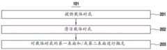
转至附图,图1展示了方法100的实施例的流程图。方法100仅是示例性的并不限于在此所展示的实施例。方法100可以应用在未在此具体描绘或描述的许多不同的实施例或示例中。在某些实施例中,可以用所展示的顺序进行方法100的活动。在其他实施例中,可以用任何其他合适的顺序进行方法100的活动。在再其他实施例中,可以组合或跳过方法100中的活动中的一项或多项活动。Turning to the drawings, FIG. 1 illustrates a flow diagram of an embodiment of a
在许多实施例中,方法100可以包括一种提供(例如,制造)电子器件的方法。虽然电子器件可以包括任何合适的电子器件,但在许多实施例中,电子器件可以包括电子显示器、X射线传感器、生物传感器、电池等。一般来讲,当在器件衬底上提供电子器件的一个或多个半导体元件时,将电子器件的器件衬底联接至载体衬底上可以方便提供电子器件。例如,在某些实施例中,当器件衬底包括柔性衬底并且载体衬底包括刚性衬底时,将电子器件的器件衬底联接到载体衬底上可以允许使用被配置成用于在刚性衬底上进行加工的半导体制造基础设施在器件衬底上提供电子器件的半导体元件。在许多实施例中,在器件衬底上提供半导体元件之后,方法100可以允许将器件衬底与载体衬底以减轻或消除电子器件上的缺陷的方式分离,如在此更详细地讨论的。In many embodiments,
例如,方法100可以包括提供载体衬底的活动101。图2展示了根据图1的实施例的示例性活动101。For example,
在许多实施例中,活动101可以包括提供载体衬底的活动201。载体衬底可以包括第一表面和与该第一表面相对的第二表面。载体衬底可以被配置成用于在将器件衬底联接到载体衬底和粘接改性层上时最小化器件衬底的弓弯、翘曲、和/或变形,如下文所述。In many embodiments,
相应地,在许多实施例中,载体衬底可以包括刚性衬底。载体衬底(例如,刚性衬底)可以包括具有如上文所限定的刚性衬底的特性的任何合适的材料。具体地,示例性材料可以包括铝(Al2O3)、硅、玻璃(例如,钡硼硅酸盐玻璃、钠钙硅酸盐玻璃和/或碱水玻璃)、金属、金属合金(例如,钢,比如像不锈钢)、和/或蓝宝石。然而,在某些实施例中,载体衬底(例如,刚性衬底)可以没有硅和/或非晶硅。同时,在许多实施例中,玻璃可以包括低CTE玻璃。Accordingly, in many embodiments, the carrier substrate may comprise a rigid substrate. The carrier substrate (eg, rigid substrate) may comprise any suitable material having the properties of a rigid substrate as defined above. Specifically, exemplary materials may include aluminum (Al2O3), silicon, glass (eg, barium borosilicate glass, soda lime silicate glass, and/or alkali water glass), metals, metal alloys (eg, steel, such as like stainless steel), and/or sapphire. However, in some embodiments, the carrier substrate (eg, rigid substrate) may be free of silicon and/or amorphous silicon. Also, in many embodiments, the glass may comprise a low CTE glass.
进一步地,还可以选择用于载体衬底(例如,刚性衬底)的材料,从而使得材料的CTE大致与器件衬底和/或粘接改性层的材料的CTE相匹配,这些中的每一个都在上文进行了简单地介绍并且在下文进行更详细的描述。同样,在某些实施例中,用于器件衬底和/或粘接改性层的材料可以被选择成CTE与载体衬底的材料相匹配、和/或彼此相匹配。非匹配的CTE会在载体衬底、器件衬底和/或粘接改性层之间产生应力。Further, the material used for the carrier substrate (eg, rigid substrate) can also be selected such that the CTE of the material approximately matches the CTE of the device substrate and/or the material of the adhesion modification layer, each of these One is briefly introduced above and described in more detail below. Also, in certain embodiments, the materials used for the device substrate and/or the adhesion modification layer may be selected to match the CTE to the material of the carrier substrate, and/or to each other. Mismatched CTEs can create stress between the carrier substrate, device substrate, and/or adhesion-modifying layer.
同样,在许多实施例中,载体衬底可以是晶片或面板。载体衬底(例如,晶片或面板)可以包括任何合适的尺寸。例如,载体衬底(例如,晶片或面板)可以包括任何合适的最大尺寸(例如,直径),比如像大约6英寸(大约15.24厘米)、大约8英寸(大约20.32厘米)、大约12英寸(大约30.48厘米)、或大约18英寸(大约45.72厘米)。在某些实施例中,载体衬底可以是大约370毫米乘以大约470毫米、大约400毫米乘以大约500毫米、大约620毫米乘以大约750毫米、大约730毫米乘以大约920毫米、大约1,000毫米乘以大约1,200毫米、大约1,000毫米乘以大约1,300毫米、大约1,300毫米乘以大约1,500毫米、大约1,500毫米乘以大约1,850毫米、大约1,870毫米乘以大约2,200毫米、大约1,950毫米乘以大约2,250毫米、大约2,160毫米乘以大约2,460毫米、大约2,200毫米乘以大约2,500毫米、大约2,880毫米乘以大约3,130毫米的面板。在某些实施例中,载体衬底(例如,晶片或面板)可以包括一定的载体衬底厚度。载体衬底厚度可以指的是在大致垂直于载体衬底的第一和第二表面的方向上测量的载体衬底的尺寸。例如,载体衬底厚度可以大于等于大约300微米并且小于等于大约2毫米。在这些或其他实施例中,载体衬底厚度可以大于等于大约0.5毫米。在许多实施例中,载体衬底厚度可以是大致恒定的。Also, in many embodiments, the carrier substrate may be a wafer or a panel. The carrier substrate (eg, wafer or panel) may comprise any suitable size. For example, the carrier substrate (eg, wafer or panel) may comprise any suitable maximum dimension (eg, diameter), such as about 6 inches (about 15.24 centimeters), about 8 inches (about 20.32 centimeters), about 12 inches (about 12 inches) 30.48 cm), or approximately 18 inches (approximately 45.72 cm). In certain embodiments, the carrier substrate may be approximately 370 millimeters by approximately 470 millimeters, approximately 400 millimeters by approximately 500 millimeters, approximately 620 millimeters by approximately 750 millimeters, approximately 730 millimeters by approximately 920 millimeters, approximately 1,000 millimeters mm by approximately 1,200 mm, approximately 1,000 mm by approximately 1,300 mm, approximately 1,300 mm by approximately 1,500 mm, approximately 1,500 mm by approximately 1,850 mm, approximately 1,870 mm by approximately 2,200 mm, approximately 1,950 mm by approximately 2,250 millimeters, approximately 2,160 millimeters by approximately 2,460 millimeters, approximately 2,200 millimeters by approximately 2,500 millimeters, approximately 2,880 millimeters by approximately 3,130 millimeters of panels. In certain embodiments, the carrier substrate (eg, wafer or panel) may comprise a certain thickness of the carrier substrate. Carrier substrate thickness may refer to a dimension of the carrier substrate measured in a direction substantially perpendicular to the first and second surfaces of the carrier substrate. For example, the carrier substrate thickness may be greater than or equal to about 300 microns and less than or equal to about 2 millimeters. In these or other embodiments, the carrier substrate thickness may be greater than or equal to about 0.5 millimeters. In many embodiments, the carrier substrate thickness may be substantially constant.
随后,在某些实施例中,活动101可以包括清洁载体衬底的活动202。在某些实施例中,活动202可以如下进行:使用等离子体(例如,氧等离子体)或使用超声波浴清洁载体衬底。Subsequently, in some embodiments,
然后,活动101可以包括对载体衬底的第一表面和/或第二表面进行抛光的活动203。如下文所述,对没有随后联接(例如,粘合)到粘接改性层上的载体衬底的表面(例如,第一表面)进行抛光提高了真空卡盘或气动卡盘操作载体衬底的能力。同样,如下文所述,对随后联接(例如,粘合)到粘接改性层上的载体衬底的表面(例如,第二表面)进行抛光去除了载体衬底的那个表面上的拓扑特征,这些拓扑特征可能造成在将器件衬底与载体衬底联接到一起之后所产生的器件衬底组件在z轴上的粗糙度。Then,
接下来,返回到图1,方法100可以包括在载体衬底的至少一部分上,比如像在载体衬底的第二表面的至少一部分(例如,全部)上提供粘接改性层的活动102。像载体衬底一样,粘接改性层可以包括第一表面和与该第一表面相对的第二表面。在这些实施例中,粘接改性层的第一表面可以位于载体衬底的第二表面附近。Next, returning to FIG. 1 ,
如下文所解释的,在各实施例中,粘接改性层可以包括能够用粘合力(即,第一粘合力)粘合到器件衬底和/或粘合到将器件衬底粘合到粘接改性层的粘接剂上(如下文所述)的任何合适的材料(例如,非晶硅、氮化硅、二氧化硅、和/或3-甲基丙烯酰氧基丙基三甲氧基硅烷等),该粘合力大于载体衬底与器件衬底和/或直接与粘接剂之间的粘合力(即,第二粘合力)。因此,粘接改性层可作为中间层进行操作,中间层被配置成使得器件衬底通过粘接改性层用比没有粘接改性层的情况下的将可能的粘合力更大的粘合力直接与载体衬底相联接。相应地,在某些示例中,可以将活动102作为以下活动的一部分来进行:对载体衬底的第二表面的至少一部分进行处理,以增加器件衬底的第一表面联接到载体衬底的第二表面的至少一部分上所用的力(即,第二粘合力)(即,增加至第一粘合力)。图3展示了根据图1的实施例的示例性活动102。As explained below, in various embodiments, the adhesion-modifying layer may include an adhesion-modifying layer capable of adhering to the device substrate with an adhesive force (ie, a first adhesion force) and/or adhering to the device substrate Any suitable material (eg, amorphous silicon, silicon nitride, silicon dioxide, and/or 3-methacryloyloxypropane) bonded to the adhesive of the adhesion-modifying layer (as described below) trimethoxysilane, etc.), the adhesion is greater than the adhesion between the carrier substrate and the device substrate and/or directly with the adhesive (ie, the second adhesion). Thus, the adhesion-modifying layer can operate as an intermediate layer configured such that the device substrate is bonded with a greater adhesion force through the adhesion-modifying layer than would be possible without the adhesion-modifying layer. The adhesive force is directly coupled to the carrier substrate. Accordingly, in some examples,
活动102可以包括在载体衬底的至少一部分上(比如像在载体衬底的第二表面的至少一部分(例如,全部))上沉积粘接改性层的活动301。在其他实施例中,活动301可以由对在器件衬底的第一表面处的粘接改性层进行沉积的活动来替代。在任一实现方式中,可以通过化学气相沉积(例如,等离子增强型化学气相沉积)来进行沉积。例如,在许多实施例中,可以在一个或多个预定条件下在载体衬底(例如,载体衬底的第二表面的至少一部分或全部或基本全部)上沉积粘接改性层。沉积的示例性条件可以包括大约0.267kPa的压力、大约170mW/cm2的功率密度、大约100标准立方厘米每分钟的硅烷流量、大约3000标准立方厘米每分钟的氢气流量、和大约2.44厘米的基座间隔。
粘接改性层可以被提供(例如,沉积)成包括一定的厚度(即,在载体衬底上提供粘接改性层时大致垂直于载体衬底的第二表面的粘接改性层的尺寸)。在许多实施例中,跨载体衬底的第二表面的厚度可以是大致恒定的。在某些实施例中,该厚度可以大于等于大约0.05微米并且小于等于大约25微米,比如像大约0.3微米。一般来讲,可以将厚度选择成足够厚以确保粘接改性层在载体衬底上的连续分布。进一步地,在仍然允许载体衬底的同时,可以将厚度选择成尽可能薄以便在将器件衬底联接到载体衬底和/或粘接改性层上时最小化器件衬底的弓弯、翘曲、和/或变形,如下文所述。The adhesion-modifying layer may be provided (eg, deposited) to include a thickness (ie, a thickness of the adhesion-modifying layer that is substantially perpendicular to the second surface of the carrier substrate when the adhesion-modifying layer is provided on the carrier substrate). size). In many embodiments, the thickness of the second surface of the carrier substrate may be substantially constant. In certain embodiments, the thickness may be greater than or equal to about 0.05 microns and less than or equal to about 25 microns, such as about 0.3 microns. In general, the thickness can be chosen to be thick enough to ensure continuous distribution of the adhesion-modifying layer on the carrier substrate. Further, while still allowing the carrier substrate, the thickness can be chosen to be as thin as possible in order to minimize bowing, bowing, Warping, and/or deformation, as described below.
在某些实施例中,活动102可以包括在粘接改性层的至少一部分(例如,粘接改性层的第二表面的至少一部分)上图案化掩模(例如,光刻胶)的活动302。掩模可以覆盖粘接改性层的不被蚀刻的一个或多个部分。例如,在如下文所述的活动303过程中,可以在粘接改性层的第二表面的周边部分上图案化掩模,从而使粘接改性层的第二表面的中央部分暴露出来。In certain embodiments,
在这些实施例中,载体衬底的周边部分可以指的是载体衬底的第二表面的位于载体衬底的边缘与载体衬底的周边之间的一部分。周边可以指的是位于载体衬底的第二表面距离载体衬底的边缘预定距离处的连续参考线。可以将预定距离选择成尽可能小以便最大化用于半导体器件的器件构建表面同时足够大以对应于载体表面的将在半导体器件的制造过程中操作的那些部分。同时,粘接改性层的中央部分可以指的是载体衬底的第二表面的对应于用于半导体器件的器件构建表面的剩余部分。In these embodiments, the peripheral portion of the carrier substrate may refer to a portion of the second surface of the carrier substrate between the edge of the carrier substrate and the perimeter of the carrier substrate. Perimeter may refer to a continuous reference line located at a predetermined distance from the second surface of the carrier substrate from the edge of the carrier substrate. The predetermined distance may be chosen to be as small as possible in order to maximize the device build surface for the semiconductor device while being large enough to correspond to those portions of the carrier surface that will be manipulated during fabrication of the semiconductor device. Meanwhile, the central portion of the adhesion-modifying layer may refer to the remaining portion of the second surface of the carrier substrate corresponding to the device building surface for the semiconductor device.
掩模可以配备有一定的厚度,从而使得掩模不会在如下所述的活动303过程中被蚀刻穿。在某些实施例中,掩模可以具有可以大于等于大约2.5微米并且小于等于大约5.0微米的厚度,比如像大约3.5微米。The mask may be provided with a thickness so that the mask is not etched through during activity 303 as described below. In certain embodiments, the mask may have a thickness that may be greater than or equal to about 2.5 microns and less than or equal to about 5.0 microns, such as about 3.5 microns.
在某些实施例中,可以通过用光刻胶涂覆粘接改性层的第二表面来进行活动302。接下来,粘接改性层可以与模板对齐,并且光刻胶可以暴露于紫外线下以将掩模图像从模板传递到光刻胶上。在传递掩模图像之后,可以烘烤光刻胶。然后,可以通过使用常规的显影化学制品来移除光刻胶由于模板而没有暴露于紫外线下的部分来显影掩模。In certain embodiments, activity 302 may be performed by coating the second surface of the adhesion-modifying layer with photoresist. Next, the adhesion-modifying layer can be aligned with the template, and the photoresist can be exposed to ultraviolet light to transfer the mask image from the template to the photoresist. After transferring the mask image, the photoresist can be baked. The mask can then be developed by using conventional development chemicals to remove portions of the photoresist that are not exposed to UV light due to the template.
接下来,活动102可以包括对粘接改性层(例如,粘接改性层的未掩模部分)进行蚀刻的活动303。在许多实施例中,可以通过对粘接改性层进行反应离子刻蚀或湿蚀刻来进行活动303。在某些示例中,可以用缓冲氧化蚀刻剂、氯基蚀刻剂、或氟基蚀刻剂来蚀刻粘接改性层。Next,
同时,在活动303之后,活动102可以包括移除掩模的活动304。在某些示例中,可以通过使用包括一种或多种溶剂(比如像丙酮、n-甲基吡咯烷酮、氨丙基吗啉、二甲亚砜、氨丙醇、和/或环丁砜等)的溶剂蚀刻溶解掩模来进行活动304。在这些或其他示例中,可以在70℃使用静态浴、再循环浴、或喷雾涂布机来进行溶剂蚀刻。然后,带有粘接改性层的剩余部分的载体衬底可以使用去离子水来冲洗并且可以被旋转干燥或风刀干燥。在某些示例中,可以在快速翻斗冲洗器中进行冲洗,并且可以在旋转冲洗干燥器中进行干燥。Meanwhile, following activity 303,
在许多实施例中,可以省略活动302至304。在某些实施例中,是否进行活动302至304可以取决于被实施用于器件衬底的材料,如下文所述。例如,当器件衬底包括聚酰亚胺时,可能期望进行活动302至304。同时,当器件衬底包括聚萘二甲酸乙二醇酯时,可能期望省略活动302至304。In many embodiments, activities 302-304 may be omitted. In certain embodiments, whether or not activities 302-304 are performed may depend on the material implemented for the device substrate, as described below. For example, it may be desirable to perform activities 302-304 when the device substrate comprises polyimide. Also, when the device substrate includes polyethylene naphthalate, it may be desirable to omit activities 302-304.
活动102可以包括对具有粘接改性层的剩余部分的载体衬底进行清洁的活动305。活动305可以如下进行:使用去离子水对带有粘接改性层的剩余部分的载体衬底进行冲洗并且对带有粘接改性层的剩余部分的载体衬底进行旋转干燥。在某些示例中,可以在快速翻斗冲洗器中进行冲洗,并且可以在旋转冲洗干燥器中进行干燥。在某些实施例中,可以将活动305省略或者作为活动304的一部分来进行。
进一步地,活动102可以包括对带有粘接改性层的剩余部分的载体衬底进行蚀刻(例如,灰化)的活动306。可以用氧等离子体蚀刻来进行活动306。在某些实施例中,氧等离子体蚀刻可以在大约1200mTorr(托)的压力下进行90分钟。在某些实施例中,可以省略活动306。Further,
在附图中暂时向前转,图4展示了根据实施例的在载体衬底401上提供粘接改性层402之后的半导体器件400的局部横截面图。半导体器件400可以与方法100(图1)的半导体器件类似或完全相同。进一步地,载体衬底401和/或粘接改性层402可以分别与方法100(图1)的载体衬底和/或粘接改性层类似或完全相同。相应地,载体衬底401可以包括第一表面403和与第一表面403相对的第二表面404。同样,粘接改性层402可以包括第一表面405和与第一表面405相对的第二表面406。Turning briefly forward in the drawings, FIG. 4 illustrates a partial cross-sectional view of a
同时,图5展示了根据实施例的半导体器件500的局部横截面图。半导体器件500可以与半导体器件400类似或完全相同,除了粘接改性层502的中央部分已经通过蚀刻被移除以留下粘接改性层502的周边部分508并且暴露出载体衬底501以外。载体衬底501可以与载体衬底401(图4)和/或方法100(图1)的载体衬底类似或完全相同;粘接改性层502可以与粘接改性层402(图4)和/或方法100(图1)的粘接改性层类似或完全相同;并且中央部分507和/或周边部分508可以分别与方法100(图1)的粘接改性层的中央部分和/或周边部分类似或完全相同。相应地,载体衬底501可以包括第一表面503和与第一表面503相对的第二表面504。同样,粘接改性层502可以包括第一表面505和与第一表面505相对的第二表面506。Meanwhile, FIG. 5 illustrates a partial cross-sectional view of a
现在返回参照图1,方法100可以包括提供器件衬底的活动103。像载体衬底一样,器件衬底可以包括第一表面和与该第一表面相对的第二表面。Referring now back to FIG. 1 ,
在许多实施例中,器件衬底可以包括柔性衬底。器件衬底(例如,柔性衬底)可以包括具有如上文所限定的柔性衬底的那些特性的任何适合的材料。具体地,示例性材料可以包括聚萘二甲酸乙二醇酯、聚对苯二甲酸乙二醇酯、聚醚砜、聚酰亚胺、聚碳酸酯、环烯烃共聚物、液晶聚合物、任何其他合适的聚合物、玻璃(比如像由美国纽约州康宁市的康宁公司(Corning Inc.)等所制造的氟硅酸盐玻璃、硼硅玻璃、康宁(Corning)玻璃、WillowTM玻璃、和/或Vitrelle玻璃等)、金属箔(例如,铝箔等)等。In many embodiments, the device substrate may comprise a flexible substrate. A device substrate (eg, a flexible substrate) may comprise any suitable material having those properties of a flexible substrate as defined above. Specifically, exemplary materials may include polyethylene naphthalate, polyethylene terephthalate, polyethersulfone, polyimide, polycarbonate, cyclic olefin copolymers, liquid crystal polymers, any Other suitable polymers, glasses (such as fluorosilicate glass, borosilicate glass, Corning glass, manufactured by Corning Inc., Corning, NY, USA) glass, Willow™ glass, and/or Vitrelle glass, etc.), metal foil (eg, aluminum foil, etc.), and the like.
在某些实施例中,活动103可以如下进行:提供器件衬底。在其他实施例中,活动103可以如下进行:在载体衬底上和在粘接改性层(例如,在粘接改性层的第二表面)上沉积器件衬底,比如像作为如下文所述的活动701(图7)的一部分。In some embodiments,
进一步地,在某些实施例中,方法100可以包括比如像(i)在载体衬底和在粘接改性层(例如,在粘接改性层的第二表面)上和/或(ii)在器件衬底的第一表面上提供粘接剂的活动104。粘接剂可以包括被配置成用于用比粘合到载体衬底上更大的粘合力粘合到粘接改性层上的任何材料。在许多示例中,粘接剂可以包括丙烯酸盐聚合物粘接剂。在某些实施例中,可以省略活动104,比如像在进行活动701(图7)时。Further, in certain embodiments,
在各实施例中,活动104可以如下进行:在粘接改性层(例如,在粘接改性层的第二表面)上和/或在器件衬底的第一表面沉积粘接剂,比如像通过旋转涂覆、喷涂、挤压涂覆、预成型层压、狭缝型模涂覆、丝网层压、丝网印刷和/或汽相涂底。在这些或其他实施例中,可以在一个或多个预定条件下将粘接剂沉积在粘接改性层(例如,在粘接改性层的第二表面)上和/或器件衬底的第一表面处。In various embodiments,
在具体示例中,可以在首先以大约1000转每分钟的旋转速率旋转具有粘接改性层的载体衬底大约25秒的时间的同时沉积粘接剂。然后,在以大约3,500转每分钟的旋转速率旋转载体衬底和粘接改性层大约20秒的时间之前可以在一定时间(例如,大约10秒)内保持载体衬底和粘接改性层静止。In a specific example, the adhesive may be deposited while first spinning the carrier substrate with the adhesion-modifying layer at a spin rate of about 1000 revolutions per minute for a period of about 25 seconds. The carrier substrate and adhesion-modifying layer may then be held for a period of time (eg, about 10 seconds) before rotating the carrier substrate and adhesion-modifying layer at a rotation rate of about 3,500 rpm for a period of about 20 seconds still.
在附图中向前转,图6展示了根据图4的实施例的在载体衬底401上和在粘接改性层402(例如,在粘接改性层402的第二表面406)上提供粘接剂609之后的半导体器件400的局部横截面图。Turning forward in the drawings, FIG. 6 illustrates on the
再次回到图1,方法100可以包括将器件衬底与载体衬底联接到一起的活动105。在这些实施例中,可以进行活动105,从而使得当器件衬底与载体衬底联接在一起时,粘接改性层位于器件衬底与载体衬底之间。相应地,在许多实施例中,可以在活动102和/或活动301(图3)之后进行活动105。图7展示了根据图1的实施例的示例性活动105。Returning again to FIG. 1, the
在某些实施例中,活动105可以包括将器件衬底直接粘合到粘接改性层上的活动701。图8展示了根据图7的实施例的示例性活动701。In certain embodiments,
活动701可以包括在粘接改性层(例如,在粘接改性层的第二表面)上沉积器件衬底的活动801,比如像通过旋转涂覆、喷涂、挤压涂覆、预成型层压、狭缝型模涂覆、丝网层压、丝网印刷和/或汽相涂底。在这些或其他实施例中,可以在一个或多个预定条件下将器件衬底沉积在粘接改性层(例如,在粘接改性层的第二表面)上。
在某些实施例中,这些预定条件可以取决于所期望的器件衬底厚度,如下文所讨论的。在具体示例中,可以在大于等于大约10秒并且小于等于大约100秒的时间内以大于等于大约500转每分钟并且小于等于大约6,000转每分钟的旋转速率旋转载体衬底的同时沉积器件衬底。例如,旋转速率可以是大约1,000转每分钟,和/或时间可以是大约25秒。In certain embodiments, these predetermined conditions may depend on the desired device substrate thickness, as discussed below. In a specific example, the device substrate may be deposited while rotating the carrier substrate at a rotation rate of about 500 revolutions per minute or greater and about 6,000 revolutions per minute or less for a period of greater than or equal to about 10 seconds and less than or equal to about 100 seconds . For example, the rotation rate may be about 1,000 revolutions per minute, and/or the time may be about 25 seconds.
在许多实施例中,活动701可以包括在粘接改性层(例如,在粘接改性层的第二表面)上固化器件衬底的活动802。例如,固化可以首先通过在大约90℃至大约150℃下热板烘烤大约10分钟、接着在大约220℃下常规烘箱烘烤大约一小时来进行。在许多实施例中,活动802可以有助于从器件衬底上移除用来进行如上所述的活动801的化学物质(例如,溶剂)。在这些或其他实施例中,活动802可以有助于将器件衬底粘合到粘接改性层上。如所期望的,器件衬底可以是热固化的和/或光固化的。在某些实施例中,可以省略活动802。In many embodiments,
在附图中暂时向前转,图9展示了根据图5的实施例的在将器件衬底910直接粘合到粘接改性层502上以及载体衬底501上之后的半导体器件500的局部横截面图。器件衬底910可以与上文关于方法100(图1)所述的器件衬底相似或完全相同。相应地,器件衬底910可以包括第一表面911和与第一表面911相对的第二表面912。第一表面911可以与方法100(图1)的器件衬底的第一表面类似或完全相同,并且第二表面912可以与方法100(图1)的器件衬底的第二表面类似或完全相同。Turning forward temporarily in the drawings, FIG. 9 shows a portion of a
现在返回图7,在其他实施例中,活动105可以包括用粘接剂将器件衬底粘合到粘接改性层上的活动702。相应地,当用活动702实施方法100时,进行活动104(图1)。值得注意的是,在许多实施例中,在进行活动701时,可以省略活动702,并且反之亦然。图10展示了根据图7的实施例的示例性活动702。Returning now to FIG. 7, in other embodiments,
在某些实施例中,活动702可以包括烘烤器件衬底的活动1001。在这些或其他实施例中,可以在一个或多个预定条件下烘烤器件衬底。在许多实施例中,可以在真空条件下和/或大于等于大约100℃并且小于等于大约200℃的温度下烘烤器件衬底。一般来讲,可以在活动1002至1006之前进行活动1001。在某些实施例中,可以省略活动1001。In some embodiments,
在许多实施例中,活动702可以包括在器件衬底的第二表面提供保护层的活动1002。在许多实施例中,保护层可以包括胶带(例如,由美国加利福尼亚州摩尔帕克市半导体设备公司(Semiconductor Equipment Corporation)所制造的产品号为18133-7.50的蓝色低粘性带(Blue Low Tack Squares))。进行活动802可以防止在进行如以下所述的活动1003时对器件衬底的第二表面造成损坏和/或污染。In many embodiments,
在活动1002之后,活动702可以继续进行将器件衬底的第一表面粘合到粘接改性层的第二表面上的活动1003。可以使用任何合适的层压技术(例如,辊压、囊压等)来进行活动1003。在许多实施例中,可以在一个或多个预定条件下进行活动1003。在许多示例中,可以在大于等于大约34kPa并且小于等于207kPa的压力下、在大于等于大约80℃并且小于等于大约140℃的温度下、和/或在大约0.45米每分钟的进给速率下进行活动1003。Following
例如,可以在大于等于大约0千帕(即,在真空中)并且小于等于大约150千帕的压力下将器件衬底的第一表面粘合到粘接改性层的第二表面上。在某些实施例中,压力可以包括大约138千帕。进一步地,在其他实施例中,可以用大于等于大约0.1米每分钟并且小于等于大约1.0米每分钟的进给速率将器件衬底的第一表面粘合到粘接改性层的第二表面。在某些实施例中,进给速率可以包括0.46米每分钟。还进一步地,可以在大于等于大约20℃并且小于等于大约100℃、160℃、220℃、350℃等(取决于器件衬底的材料)的温度下将器件衬底的第一表面粘合到粘接改性层的第二表面上。例如,温度在当器件衬底包括聚萘二甲酸乙二醇酯时可以小于等于大约220℃(例如,大约100℃)、在当器件衬底包括聚对苯二甲酸乙二醇酯时可以小于等于大约160℃(例如,大约100℃)、并且在当器件衬底包括聚醚砜时可以小于等于大约350℃(例如,大约100℃)。For example, the first surface of the device substrate can be bonded to the second surface of the adhesion-modifying layer at a pressure of greater than or equal to about 0 kPa (ie, in a vacuum) and less than or equal to about 150 kPa. In certain embodiments, the pressure may include about 138 kilopascals. Further, in other embodiments, the first surface of the device substrate may be bonded to the second surface of the adhesion modification layer with a feed rate of greater than or equal to about 0.1 meters per minute and less than or equal to about 1.0 meters per minute . In some embodiments, the feed rate may include 0.46 meters per minute. Still further, the first surface of the device substrate may be bonded to the device at a temperature of about 20°C or more and less than or equal to about 100°C, 160°C, 220°C, 350°C, etc. (depending on the material of the device substrate). Adhesion to the second surface of the modified layer. For example, the temperature may be less than or equal to about 220°C (eg, about 100°C) when the device substrate includes polyethylene naphthalate and less than or equal to when the device substrate includes polyethylene terephthalate Equal to about 160°C (eg, about 100°C), and may be equal to or less than about 350°C (eg, about 100°C) when the device substrate includes polyethersulfone.
适用于固化粘接剂的任何技术(例如,光固化、热固化、压力固化等)来进行活动1004,而无不损坏载体衬底、粘接改性层或器件衬底。例如,在某些实施例中,活动1005可以如下进行:比如像使用由美国康涅狄格州托灵顿市的戴马士公司(Dymax Corporation)所制造的戴马士紫外线固化系统(Dymax ultraviolet cure system)对粘接剂进行紫外线固化。在这些实施例中,活动1004可以进行大约20秒至大约180秒。在其他实施例中,活动1004可以如下进行:在烘箱(比如像由美国加利福尼亚州圣克拉拉市的美国雅马拓(Yamato)科技股份有限公司所制造的雅马拓烘箱)中烘烤粘接剂。
在活动1003和/或活动1004之后,活动702可以包括从半导体器件上移除过剩的粘接剂的活动1005。在某些实施例中,活动1005可以如下进行:使用等离子体(例如,氧等离子体)或使用超声波浴清洁载体衬底。After
在活动1003之后,活动702可以包括移除器件衬底的第二表面处的保护层的活动1006。在某些实施例中,可以省略活动1002和1005。在各实施例中,可以将活动1006作为活动1005的一部分来进行。Following
在附图中向前转,图11展示了根据图4的实施例的在用粘接剂609将器件衬底1110粘合到粘接改性层402上并且将器件衬底粘合在载体衬底401上之后的半导体器件400的局部横截面图。器件衬底1110可以与器件衬底910和/或上文关于方法100(图1)所描述的器件衬底相似或完全相同。相应地,器件衬底1010可以包括第一表面1111和与第一表面1111相对的第二表面1112。第一表面1111可以与第一表面911(图9)和/或方法100(图1)的器件衬底的第一表面类似或完全相同,并且第二表面912可以与第二表面912(图9)和/或方法100(图1)的器件衬底的第二表面类似或完全相同。Turning forward in the drawings, FIG. 11 illustrates in-process bonding of
现在再次返回图1,无论是根据活动701(图7)还是活动702(图7)实施方法100,器件衬底都可以被提供成包括一定的器件衬底厚度(即,载体衬底或粘接剂上的器件衬底的尺寸,如果适用的话,该尺寸在器件衬底联接到载体衬底上时大致垂直于载体衬底或粘接剂)。值得注意的是,为了引用目的,器件衬底厚度的计算不包含当已经将粘接改性层的中央部分移除时器件衬底在粘接改性层的周边部分上的部分,沿着该部分将要比器件衬底厚度小大约等于粘接改性层厚度的量。在许多实施例中,器件衬底厚度可以是大致恒定的。同样,器件衬底在粘接改性层的周边部分上的部分的厚度也可以是大致恒定的。在某些实施例中,载体衬底厚度可以大于等于大约1微米并且小于等于大约1毫米。例如,器件衬底厚度可以是大约20微米。一般来讲,可以将器件衬底厚度选择成足够厚以确保器件衬底在载体衬底上的连续分布。进一步地,在仍然允许以上内容的同时,可以将器件衬底厚度选择成尽可能薄以便在将器件衬底联接到载体衬底上时最小化器件衬底的弓弯、翘曲、和/或变形。Returning now to FIG. 1 again, whether
在活动105之后,方法100可以包括在将器件衬底联接至载体衬底上的同时对器件衬底进行固化的活动106。如所期望的,器件衬底可以是热固化的和/或光固化的。例如,在许多实施例中,首先,可以首先在真空条件下、在大于等于大约100℃并且小于等于大约235℃的温度下、和/或在大于等于大约1小时并且小于等于大约8小时的时间内对器件衬底进行热固化。例如,温度可以包括大约180℃或220℃,和/或时间可以包括大约3小时。Following
接下来,方法100可以包括在将器件衬底联接至载体衬底上的同时在器件衬底上提供一个或多个半导体元件的活动107。在某些实施例中,可以根据不超出200℃的温度的任何常规半导体制造工艺在器件衬底上提供半导体元件。在进一步的实施例中,可以根据不超出235℃的温度的任何常规半导体制造工艺在器件衬底上提供半导体元件。例如,在各实施例中,可以根据在以下专利申请中所描述的半导体制造工艺在器件衬底上提供半导体元件:(i)于2012年3月15日公开的美国专利申请公开序列号US 20120061672,(ii)于2012年10月11日公开的国际专利申请公开序列号WO 20121381903,和/或(iii)在2013年6月6日公开的国际专利申请公开序列号WO 2013082138,这些专利申请中的每一个专利申请的全部内容都将通过引用合并于此。在某些实施例中,可以在活动105之后进行活动107。进一步地,可以在活动108和/或活动110之前进行活动107。图12展示了根据图4的实施例的在器件衬底1110上提供一个或多个半导体元件1213之后的半导体器件400的局部横截面图;以及图13展示了根据图5的实施例的在器件衬底910上提供一个或多个半导体元件1313之后的半导体器件500的局部横截面图。Next,
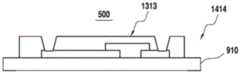
再次参照图1,在某些实施例中,方法100可以包括将器件衬底的器件部分与器件衬底的非器件部分切断的活动108(例如,在上文关于周边部分和中央部分所讨论的载体衬底的周边内的位置上)。可以将器件衬底的非器件部分粘合到粘接改性层上。同时,可以将器件衬底的器件部分仅粘合到载体衬底上。器件部分包括半导体元件的至少一部分。在某些实施例中,非器件部分可以包括半导体元件的一部分。可以使用任何合适的切割工具(例如,刀片、激光器等)将器件衬底的器件部分与器件衬底的非器件部分切断。在许多实施例中,可以进行活动108,从而使得在进行活动110(下文)时,半导体元件的某些或全部与器件衬底的器件部分保持在一起(例如,尽可能少地留下半导体元件与器件衬底的非器件部分在一起)。在许多实施例中,活动108可以发生在活动107之后。进一步地,活动108可以发生在活动110之前。Referring again to FIG. 1 , in some embodiments,
在某些实施例中,可以省略活动108,比如像当用活动702(图7)实施方法100时。在许多实施例中,当方法100被实施成包括活动701(图7)和/或活动302至304(图3)中的一个或多个活动时,方法100还可以包括活动108。图14展示了根据图5的实施例的在将器件衬底910的器件部分1414与器件衬底910的非器件部分1415切断之后的半导体器件500的局部横截面图。In some embodiments,
再次参照图1,在某些实施例中,方法100可以包括降低第一粘合力或第二粘合力中的至少一个粘合力的活动109。在这些实施例中,活动109可以如下进行:对粘接剂或粘接改性层进行化学处理、电磁处理(例如,通过紫外线或其他形式的电磁辐射,比如像激光电磁辐射)、或热处理(例如,使用激光发送电子着塑(EPLaRTM)、使用激光退火/冲蚀表面释放技术(SUFTLATM)等)。Referring again to FIG. 1 , in certain embodiments,
在许多实施例中,可以省略活动109。当使用活动109实施方法100时,在活动110之前进行活动109,如下文所述。在某些实施例中,活动109可以发生在活动108之后,或者反之亦然。In many embodiments,
接下来,方法100可以包括将器件衬底(或在适用时,器件衬底的器件部分)与载体衬底分离(例如,机械地)的活动110。图15展示了根据图4的实施例的在提供半导体元件1213之后并且在将器件衬底1110与载体衬底401(图4)分离之后的半导体元件400的器件衬底1110的横截面图;以及图16展示了根据图5的实施例的在提供半导体元件1313之后并且在将器件部分1414与载体衬底501(图5)分离之后的半导体元件500的器件衬底910的器件部分1414的横截面图。Next,
在许多实施例中,活动110可以如下进行:向器件衬底(或在适用时,器件衬底的器件部分)施加释放力(例如,稳定的释放力)。在许多实施例中,如果适用的话,可以通过从粘接改性层和/或载体衬底上剥离(例如,用手)器件衬底(或在适用时,器件衬底的器件部分)来向器件衬底(或在适用时,器件衬底的器件部分)施加释放力。在这些或其他实施例中,如果适用的话,可以通过在器件衬底(或在适用时,器件衬底的器件部分)下插入刀片并且在远离粘接改性层和/或载体衬底的方向上在器件衬底上按压(或在适用时,器件衬底的器件部分)来施加(或增强)释放力。In many embodiments,
进一步地,在这些或其他实施例中,活动110可以如下进行:比如像使用任何合适的切割工具(例如,刀片、激光器等)将器件衬底(或在适用时,器件衬底的器件部分)与粘接改性层和/或载体衬底切断。将器件衬底(或在适用时,器件衬底的器件部分)与粘接改性层和/或载体衬底切断可以替代向器件衬底(或在适用时,器件衬底的器件部分)施加释放力的活动或作为其一部分来进行。Further, in these or other embodiments,
在许多实施例中,在进行活动110时保持器件衬底(或在适用时,器件衬底的器件部分)与粘接改性层和/或载体衬底之间的小于等于大约45度的角可以减轻或防止对器件衬底(或在适用时,器件衬底的器件部分)上的半导体元件造成损害。In many embodiments, an angle of less than or equal to about 45 degrees is maintained between the device substrate (or, where applicable, the device portion of the device substrate) and the adhesion-modifying layer and/or the carrier substrate while the
进一步地,有利的是,在许多实施例中,可以在不首先比如像通过对粘接剂或粘接改性层进行化学处理、电磁处理(例如,通过紫外线或其他形式的电磁辐射,比如像激光电磁辐射)、或热处理(例如,使用激光发送电子着塑(例如,EPLaRTM工艺)、使用激光退火/冲蚀表面释放技术(例如,SUFTLATM工艺)等)(例如,修改粘接剂或粘接改性层的结构)来降低第一粘合力和/或第二粘合力的情况下进行活动110。换言之,第一粘合力和/或第二粘合力可以直接保持大致恒定(并且在许多示例中,至少保持足够低以允许机械脱粘),一直直到进行活动110。相应地,通过避免使用化学处理、电磁处理、或热处理,可以降低或消除由于使用这种化学处理、电磁处理、或热处理所导致的半导体元件的器件缺陷和/或降低的半导体元件成品率。例如,电磁处理可以通过热变形和/或形成颗粒碎屑而破坏半导体元件。同时,化学处理可以通过使半导体元件暴露在化学产品下而损坏半导体元件,从而造成半导体元件退化。而且,使用化学处理可能要求后续的清洁以便从半导体元件上移除任何残留的化学产品,和/或可能不允许器件衬底(或在适用时,器件衬底的器件部分)在分离过程中保持大致扁平,因为在将器件衬底(或在适用时,器件衬底的器件部分)浸入化学产品中的同时物理地约束器件衬底(或在适用时,器件衬底的器件部分)会具有挑战性。Further, advantageously, in many embodiments, the adhesive or adhesion-modifying layer can be treated without first, such as by chemical treatment, electromagnetic treatment (eg, by ultraviolet light or other forms of electromagnetic radiation, such as by laser electromagnetic radiation), or thermal treatment (eg, using laser-transmitted electron molding (eg, EPLaR™ process), using laser annealing/erosion surface release techniques (eg, SUFTLA™ process), etc.) (eg, modifying the adhesive or
进一步地,方法100可以包括比如像清洁载体衬底和/或粘接改性层的活动111,以便从载体衬底和/或粘接改性层上移除在进行活动110之后剩余的器件层、粘接剂、和/或半导体元件的残留部分。在某些实施例中,活动111可以如下进行:使用等离子体(例如,氧等离子体)或使用超声波浴清洁载体衬底和/或粘接改性层。相应地,在许多实施例中,可以使用同一载体衬底和/或粘接改性层来重复方法100一次或多次。Further, the
在各实施例中,当用活动104(即,使用粘接剂粘合)来实施方法100时,粘接改性层可操作用于允许将器件衬底与载体衬底分离(例如,通过活动110),从而使得在刚刚分离之后或由于分离,很少或没有粘接剂留在器件衬底的第一表面上(即,无需进行额外的制造活动来移除粘接剂)。例如,在某些实施例中,在刚刚分离之后或由于分离,少于百分之五、百分之三、百分之二或百分之一的粘接剂留在器件衬底的第一表面上。同时,在这些或其他实施例中,在分离之后,载体衬底可以保持联接到粘接改性层上,并且部分、大部分、基本上全部或全部粘接剂可以保持联接到粘接改性层上。In various embodiments, when
一般来讲,在使用粘接剂实施涉及将器件衬底(例如,柔性衬底,比如像聚萘二甲酸乙二醇酯、聚对苯二甲酸乙二醇酯、玻璃等)联接至载体衬底(例如,刚性衬底)上以及将器件衬底与载体衬底分离的用于制造电子器件的常规技术时,在分离之后留在器件衬底上的残留粘接剂会导致电子器件产品中的一部分或全部有缺陷。此类缺陷可以(i)降低器件制造成品率和/或(ii)增加为了移除这种残留粘接剂所需要的制造复杂度、时间和/或成本。然后,因为单独地方法100的粘接改性层与器件衬底和/或粘接剂的粘合力大于器件衬底和/或粘接剂与载体衬底之间的粘合力,在实施方法100时,在刚刚分离之后或由于分离,很少或没有粘接剂留在器件衬底上。相应地,因为方法100可以被实施成使得在刚刚分离之后或由于分离,很少或没有粘接剂留在器件衬底上,可以减少器件缺陷并且增加器件制造成品率,而无需会增加制造电子器件的复杂度、时间和/或成本的额外制造活动。In general, implementing using an adhesive involves coupling a device substrate (eg, a flexible substrate such as polyethylene naphthalate, polyethylene terephthalate, glass, etc.) to a carrier substrate On substrates (eg, rigid substrates) and in conventional techniques for the manufacture of electronic devices that separate the device substrate from the carrier substrate, residual adhesive left on the device substrate after separation can cause problems in electronic device products. some or all of it is defective. Such defects can (i) reduce device manufacturing yield and/or (ii) increase the manufacturing complexity, time and/or cost required to remove such residual adhesive. Then, since the adhesion of the adhesion-modifying layer of the
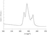
在附图中向前转,图17至图20提供了通过傅里叶变换红外光谱法凭经验展示了在实施方法100(图1)时器件衬底处的残留粘接剂的减少的各种图表。图17至图20的图表中的每一个图表示出了根据波数变化的吸收率,其中,波数是以厘米的倒数为单位进行测量的,并且吸收率是以任意单位测量的。Turning forward in the drawings, FIGS. 17-20 provide various empirically demonstrated reductions in residual adhesive at the device substrate by Fourier Transform Infrared Spectroscopy in implementing method 100 (FIG. 1) chart. Each of the graphs of FIGS. 17-20 shows absorptivity as a function of wavenumber, where wavenumber is measured in units of inverse centimeters, and absorbance is measured in arbitrary units.
具体来讲,图17是通过傅里叶变换红外光谱法展示了根据将聚萘二甲酸乙二醇酯(PEN)器件衬底粘合到硅载体衬底上的固化粘接剂的波数变化的吸收率的图表,其中减去了硅载体衬底和器件衬底的频谱。值得注意的是,聚萘二甲酸乙二醇酯(PEN)器件衬底在相关区域中是基本上透明的。在相关区域之外的低波数具有过多的吸收带。在相关区域中的峰值对应于碳氢伸缩振动,其中,振动的频率取决于粘合到碳原子上的氢原子的数量以及碳原子的粘合安排。Specifically, FIG. 17 is a graph showing, by Fourier Transform Infrared Spectroscopy, the change in wave number according to the cured adhesive bonding a polyethylene naphthalate (PEN) device substrate to a silicon carrier substrate Graph of absorbance with the spectrum of silicon carrier substrate and device substrate subtracted. Notably, the polyethylene naphthalate (PEN) device substrate is substantially transparent in the relevant regions. Low wavenumbers outside the relevant region have excessive absorption bands. The peaks in the relevant region correspond to hydrocarbon stretching vibrations, where the frequency of the vibrations depends on the number of hydrogen atoms bonded to the carbon atoms and the bonding arrangement of the carbon atoms.
转到下一个图,图18是展示了图17的相关区域的图表。在相关区域中粘接剂的吸收率有四个主峰。Turning to the next figure, FIG. 18 is a diagram showing the relevant regions of FIG. 17 . There are four main peaks in the absorbance of the adhesive in the relevant region.
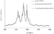
转到下一个图,图19是通过傅里叶变换红外光谱法展示了根据以下各项的波数变化的吸收率的图表:(i)未加工的聚萘二甲酸乙二醇酯(PEN)器件衬底;(ii)在具有非晶硅(a-Si)粘接改性层的硅载体衬底上加工并且与硅载体衬底分离的聚萘二甲酸乙二醇酯(PEN)器件衬底;以及(iii)在不具有非晶硅(a-Si)粘接改性层的硅载体衬底上加工并且与硅载体衬底分离的聚萘二甲酸乙二醇酯器件衬底。Turning to the next figure, Figure 19 is a graph showing absorbance by Fourier transform infrared spectroscopy as a function of wavenumber for: (i) raw polyethylene naphthalate (PEN) devices A substrate; (ii) a polyethylene naphthalate (PEN) device substrate processed on a silicon carrier substrate with an amorphous silicon (a-Si) adhesion modification layer and separated from the silicon carrier substrate and (iii) a polyethylene naphthalate device substrate processed on a silicon carrier substrate without an amorphous silicon (a-Si) adhesion modification layer and separated from the silicon carrier substrate.
再次转到下一个图,图20是通过傅里叶变换红外光谱法展示了根据以下各项的波数变化的吸收率的图表:(i)在不具有非晶硅粘接改性层的硅载体衬底上加工的第一聚萘二甲酸乙二醇酯(PEN)器件衬底,其中已经将聚萘二甲酸乙二醇酯(PEN)器件衬底与硅载体衬底分离,并且已经减去了第二聚萘二甲酸乙二醇酯(PEN)器件衬底的频谱;(ii)在将聚萘二甲酸乙二醇酯(PEN)器件衬底与硅载体衬底脱粘之后留在硅载体衬底上的固化粘接剂,其中减去了硅载体衬底的频谱;以及(iii)在具有非晶硅粘接改性层的硅载体衬底上加工的第一聚萘二甲酸乙二醇酯(PEN)器件衬底,其中已经将聚萘二甲酸乙二醇酯(PEN)器件衬底与硅载体衬底分离,并且已经减去了第二未加工的聚萘二甲酸乙二醇酯(PEN)器件衬底的频谱。为清晰起见,在图20中以降序示出了项(i)至(iii)。值得注意的是,对于项(iii),所有的四个峰值都缺失。同时,在项(i)和(iii)上的额外峰可以归因于第一聚萘二甲酸乙二醇酯(PEN)器件衬底与第二未加工的聚萘二甲酸乙二醇酯(PEN)器件衬底之间的厚度和/或成分上的细微差别。Turning again to the next figure, Figure 20 is a graph showing absorbance by Fourier transform infrared spectroscopy as a function of wavenumber: (i) on a silicon support without an amorphous silicon adhesion modification layer A first polyethylene naphthalate (PEN) device substrate processed on a substrate, wherein the polyethylene naphthalate (PEN) device substrate has been separated from the silicon carrier substrate and has been subtracted spectrum of the second polyethylene naphthalate (PEN) device substrate; (ii) left on the silicon after debonding the polyethylene naphthalate (PEN) device substrate from the silicon carrier substrate A cured adhesive on a carrier substrate in which the spectrum of the silicon carrier substrate is subtracted; and (iii) a first polyethylene naphthalate processed on a silicon carrier substrate with an amorphous silicon adhesion modification layer A glycol ester (PEN) device substrate, wherein the polyethylene naphthalate (PEN) device substrate has been separated from the silicon carrier substrate and a second raw polyethylene naphthalate has been subtracted Spectrum of alcohol ester (PEN) device substrates. Items (i) to (iii) are shown in descending order in Figure 20 for clarity. Notably, for term (iii), all four peaks are missing. Meanwhile, the additional peaks on items (i) and (iii) can be attributed to the first polyethylene naphthalate (PEN) device substrate and the second unprocessed polyethylene naphthalate (PEN) PEN) minor differences in thickness and/or composition between device substrates.
同时,在这些实施例中或在其他实施例中,比如像在不进行活动104(即,无需粘接剂)但是进行例如活动701(例如,在粘接改性层上直接沉积器件衬底)的情况下实施方法100,粘接改性层可以操作用于在活动107过程中防止器件衬底的过早分离。在各示例中,在实施涉及将器件衬底(例如,柔性衬底,比如像聚醚砜)联接(例如,通过直接沉积)至载体衬底(例如,刚性衬底,比如像玻璃)上以及将器件衬底与载体衬底分离的用于制造半导体的常规技术时,经常通过改变器件衬底的配方来控制器件衬底到载体衬底上的粘合力。然而,器件衬底配方的批次到批次的变化分离有时会导致器件衬底与载体衬底分离比所期望的要更快。例如,器件衬底的机器操作有时会导致器件衬底与载体衬底分离比所期望的要更快。器件衬底与载体衬底的过早分离还会造成器件缺陷和图案变形,这降低了器件制造成品率。有利的是,因为单独地方法100的粘接改性层与器件衬底的粘合力大于器件衬底与载体衬底之间粘合力,可以防止过早分离,从而产生更少的器件缺陷和更少的图案变形。Also, in these embodiments or in other embodiments, such as when
值得注意的是,虽然粘接改性层通常被描述为增加载体衬底上的粘合力,在一种替代方法中,粘接改性层可以被沉积在器件衬底上并且被配置成用于降低粘合力。在这些实施例中,当器件衬底是柔性衬底时,将从将不会干扰器件衬底的柔性的材料中选择粘接改性层。It is worth noting that while adhesion-modifying layers are often described as increasing adhesion on a carrier substrate, in an alternative approach, an adhesion-modifying layer can be deposited on a device substrate and configured to to reduce adhesion. In these embodiments, when the device substrate is a flexible substrate, the adhesion-modifying layer will be selected from materials that will not interfere with the flexibility of the device substrate.
进一步地,在此所披露的方法(例如,方法100(图1))和半导体器件(例如,半导体器件400(图4、图6、图11、图12和图15)和/或半导体器件500(图5、图9、图13、图14和图16))可以特别良好地适用于实施半导体制造,其中,半导体制造受到上限温度的约束(比如像由于正在使用的材料)。例如,当是柔性衬底时,许多器件衬底(包括上文所提供的示例性器件衬底材料中的许多材料)可以排除高于某些温度的制造。在某些实施例中,半导体制造中的某些或全部可能不能超出大约160℃、180℃、200℃、220℃、250℃、或350℃。Further, methods disclosed herein (eg, method 100 ( FIG. 1 )) and semiconductor devices (eg, semiconductor device 400 ( FIG. 4 , FIG. 6 , FIG. 11 , FIG. 12 , and FIG. 15 ) and/or semiconductor device 500 (Fig. 5, Fig. 9, Fig. 13, Fig. 14 and Fig. 16)) may be particularly well suited for implementing semiconductor fabrication, where semiconductor fabrication is constrained by an upper temperature limit (such as due to the materials being used). For example, when a flexible substrate, many device substrates, including many of the exemplary device substrate materials provided above, may preclude fabrication above certain temperatures. In certain embodiments, some or all of the semiconductor fabrication may not exceed approximately 160°C, 180°C, 200°C, 220°C, 250°C, or 350°C.
可以良好地适用于实施此所披露的方法(例如,方法100(图1))和半导体器件(例如,半导体器件400(图4、图6、图11、图12和图15)和/或半导体器件500(图5、图9、图13、图14和图16))的各种半导体制造工艺和器件在以下参考文献中进行了描述,这些参考文献中的每一个参考文献的披露内容通过引用以其全文结合于此:(i)于2011年9月22日公开的美国专利申请公开序列号US 20110228492,(ii)于2013年10月17日公开的美国专利申请公开序列号US 20130271930,(iii)于2012年3月15日公开的美国专利申请公开序列号US20120061672,(iv)于2014年1月9日公开的美国专利申请公开序列号US 20140008651,(v)于2013年6月6日公开的国际专利申请公开序列号WO 2013082138,(vi)于2014年3月6日公开的美国专利申请公开序列号US 20140065389,(vii)于2013年3月28日公开的美国专利申请公开序列号US 20130075739,(viii)于2011年3月17日公开的美国专利申请公开序列号US 20110064953,(ix)于2010年11月25日公开的美国专利申请公开序列号US20100297829,(x)于2010年10月21日公开的美国专利申请公开序列号US 20100264112,(xi)于2011年3月24日公开的美国专利申请公开序列号US 20110068492,(xii)于2011年5月31日公开的美国专利申请公开序列号US 20060194363,以及(xiii)于2011年2月3日公开的美国专利申请公开序列号US 20110023672。may be well suited for implementing the methods disclosed herein (eg, method 100 ( FIG. 1 )) and semiconductor devices (eg, semiconductor device 400 ( FIG. 4 , FIG. 6 , FIG. 11 , FIG. 12 , and FIG. 15 ) and/or semiconductor devices Various semiconductor fabrication processes and devices for device 500 (FIGS. 5, 9, 13, 14, and 16)) are described in the following references, the disclosures of each of which are incorporated by reference Incorporated herein in their entirety: (i) US Patent Application Publication Serial No. US 20110228492, published September 22, 2011, (ii) US Patent Application Publication No. US 20130271930, published October 17, 2013, ( iii) US Patent Application Publication Serial No. US20120061672 published on March 15, 2012, (iv) US Patent Application Publication Serial No. US 20140008651 published on January 9, 2014, (v) June 6, 2013 Published International Patent Application Publication No. WO 2013082138, (vi) US Patent Application Publication Serial No. US 20140065389 published on March 6, 2014, (vii) US Patent Application Publication Serial No. published on March 28, 2013 US 20130075739, (viii) US Patent Application Publication Serial No. US 20110064953 published on March 17, 2011, (ix) US Patent Application Publication Serial No. US20100297829 published on November 25, 2010, (x) in 2010 US Patent Application Publication No. US 20100264112 published on October 21, (xi) US Patent Application Publication No. US 20110068492 published on March 24, 2011, (xii) US Patent published on May 31, 2011 Application Publication Serial No. US 20060194363, and (xiii) US Patent Application Publication Serial No. US 20110023672 published on February 3, 2011.
尽管已经参考特定实施例描述了本发明,但是应理解到本领域内的技术人员可以在不脱离本发明的精神和范围的情况下进行各种改变。相应地,本发明的实施例的披露旨在说明本发明的范围而不在于限制。在此的意图是本发明的范围应当仅限于所附权利要求所要求的内容。例如,对于本领域的普通技术人员而言,非常明显的是方法100(图1)的一项或多项活动可以由许多不同的活动、程序和/或流程组成,并且可以由许多不同模块且以许多不同的顺序进行,可以对图1至图20的任何元件进行修改,并且这些实施例中的某些实施例的前面的讨论不一定代表全部可能实施例的完整描述。While the present invention has been described with reference to specific embodiments, it will be understood that various changes can be made by those skilled in the art without departing from the spirit and scope of the invention. Accordingly, the disclosure of the embodiments of the present invention is intended to illustrate the scope of the present invention and not to limit it. It is intended here that the scope of the present invention should be limited only as required by the appended claims. For example, it will be apparent to those of ordinary skill in the art that one or more of the activities of method 100 (FIG. 1) may be composed of many different activities, procedures and/or processes, and may be composed of many different modules and Modifications may be made to any of the elements of FIGS. 1-20 in many different orders, and the preceding discussion of some of these embodiments does not necessarily represent a complete description of all possible embodiments.
通常,一个或多个要求的元件的替代构成重构而不是修复。此外,已经就特定实施例描述了益处、其他优点以及问题的解决方案。然而,不能认为可以引起任何益处、优点、或解决方案发生或变得更明显的益处、优点、问题解决方案以及任何元件或多个元件是任何或全部权利要求的关键的、要求的、或必要的特征或元素,除非在此类权利要求中陈述了此类益处、优点、解决方案或元件。Typically, replacement of one or more of the required elements constitutes a reconstruction rather than a repair. Furthermore, benefits, other advantages, and solutions to problems have been described with respect to specific embodiments. However, no benefit, advantage, solution to the problem, nor any element or elements that could cause any benefit, advantage, or solution to occur or become apparent is to be considered critical, required, or essential to any or all of the claims features or elements unless such benefits, advantages, solutions or elements are recited in such claims.
并且,若实施例和/或限制如下,则在此所披露的实施例和限制不是在专用原则下而为大众所专用:(1)未在权利要求书中清楚地要求;及(2)是或在等同原则下是权利要求书中提及的元件和/或限制的潜在等效物。Also, the embodiments and/or limitations disclosed herein are not intended to be used by the general public under the exclusive doctrine of: (1) not expressly required in the claims; and (2) are or potential equivalents to the elements and/or limitations recited in the claims under the doctrine of equivalents.
Claims (22)
Translated fromChinese


Applications Claiming Priority (3)
| Application Number | Priority Date | Filing Date | Title |
|---|---|---|---|
| US201461992799P | 2014-05-13 | 2014-05-13 | |
| US61/992,799 | 2014-05-13 | ||
| PCT/US2015/029991WO2015175353A1 (en) | 2014-05-13 | 2015-05-08 | Method of providing an electronic device and electronic device thereof |
Publications (2)
| Publication Number | Publication Date |
|---|---|
| CN106663640A CN106663640A (en) | 2017-05-10 |
| CN106663640Btrue CN106663640B (en) | 2020-01-07 |
Family
ID=54480477
Family Applications (1)
| Application Number | Title | Priority Date | Filing Date |
|---|---|---|---|
| CN201580038025.3AActiveCN106663640B (en) | 2014-05-13 | 2015-05-08 | Method of providing electronic device and electronic device thereof |
Country Status (7)
| Country | Link |
|---|---|
| US (1) | US9953951B2 (en) |
| EP (1) | EP3143641A4 (en) |
| JP (1) | JP2017518638A (en) |
| KR (1) | KR102466741B1 (en) |
| CN (1) | CN106663640B (en) |
| TW (1) | TWI671832B (en) |
| WO (1) | WO2015175353A1 (en) |
Families Citing this family (10)
| Publication number | Priority date | Publication date | Assignee | Title |
|---|---|---|---|---|
| US9721825B2 (en) | 2008-12-02 | 2017-08-01 | Arizona Board Of Regents, A Body Corporate Of The State Of Arizona, Acting For And On Behalf Of Arizona State University | Method of providing a flexible semiconductor device and flexible semiconductor device thereof |
| US9991311B2 (en) | 2008-12-02 | 2018-06-05 | Arizona Board Of Regents On Behalf Of Arizona State University | Dual active layer semiconductor device and method of manufacturing the same |
| US10381224B2 (en) | 2014-01-23 | 2019-08-13 | Arizona Board Of Regents On Behalf Of Arizona State University | Method of providing an electronic device and electronic device thereof |
| WO2017034644A2 (en) | 2015-06-09 | 2017-03-02 | ARIZONA BOARD OF REGENTS a body corporate for THE STATE OF ARIZONA for and on behalf of ARIZONA STATE UNIVERSITY | Method of providing an electronic device and electronic device thereof |
| WO2015156891A2 (en) | 2014-01-23 | 2015-10-15 | Arizona Board Of Regents, Acting For And On Behalf Of Arizona State University | Method of providing a flexible semiconductor device and flexible semiconductor device thereof |
| US9741742B2 (en) | 2014-12-22 | 2017-08-22 | Arizona Board Of Regents, A Body Corporate Of The State Of Arizona, Acting For And On Behalf Of Arizona State University | Deformable electronic device and methods of providing and using deformable electronic device |
| US10446582B2 (en) | 2014-12-22 | 2019-10-15 | Arizona Board Of Regents On Behalf Of Arizona State University | Method of providing an imaging system and imaging system thereof |
| WO2017218898A2 (en) | 2016-06-16 | 2017-12-21 | Arizona Board Of Regents On Behalf Of Arizona State University | Electronic devices and related methods |
| CN111349400A (en)* | 2018-12-21 | 2020-06-30 | 达迈科技股份有限公司 | A kind of double-layer adhesive film, multilayer pressure-sensitive adhesive composite film and preparation method thereof for electronic component manufacturing process |
| CN112967992B (en)* | 2020-12-07 | 2022-09-23 | 重庆康佳光电技术研究院有限公司 | Transfer method of epitaxial structure |
Citations (5)
| Publication number | Priority date | Publication date | Assignee | Title |
|---|---|---|---|---|
| CN101027751A (en)* | 2004-09-24 | 2007-08-29 | 株式会社半导体能源研究所 | Semiconductor device and method for manufacturing the same |
| CN101785086A (en)* | 2007-09-20 | 2010-07-21 | 夏普株式会社 | Method for manufacturing display device and laminated structure |
| CN101925996A (en)* | 2008-01-24 | 2010-12-22 | 布鲁尔科技公司 | Method of reversibly mounting a device wafer on a carrier substrate |
| CN101944477A (en)* | 2009-07-03 | 2011-01-12 | 鸿富锦精密工业(深圳)有限公司 | Manufacturing method for flexible semiconductor device |
| CN102422406A (en)* | 2009-05-06 | 2012-04-18 | 康宁股份有限公司 | Supports for glass substrates |
Family Cites Families (203)
| Publication number | Priority date | Publication date | Assignee | Title |
|---|---|---|---|---|
| US3089801A (en) | 1957-05-27 | 1963-05-14 | Minnesota Mining & Mfg | Ultra-thin glass sheet |
| US3684637A (en) | 1970-12-18 | 1972-08-15 | Albert E Anderson | Simulated leather laminate and its preparation |
| US3723635A (en) | 1971-08-16 | 1973-03-27 | Western Electric Co | Double-sided flexible circuit assembly and method of manufacture therefor |
| US4337107A (en) | 1980-06-16 | 1982-06-29 | Minnesota Mining And Manufacturing Company | Abrasion-resistant transfer laminating sheet material |
| DE3104623A1 (en) | 1981-02-10 | 1982-08-26 | Robert Bosch Gmbh, 7000 Stuttgart | METHOD FOR FASTENING COMPONENTS WITH FLAT CONNECTORS AND COMPONENT HERE |
| US4349593A (en) | 1981-04-06 | 1982-09-14 | Penn-Gil Fabrics, Inc. | Double knit fabric processing into decorative goods |
| US5220488A (en) | 1985-09-04 | 1993-06-15 | Ufe Incorporated | Injection molded printed circuits |
| US5098772A (en) | 1986-06-13 | 1992-03-24 | Af Strom Oscar B F | Composite sheet for transfer of an image from same to a substrate |
| US4858073A (en) | 1986-12-10 | 1989-08-15 | Akzo America Inc. | Metal substrated printed circuit |
| JP2517040B2 (en) | 1988-02-03 | 1996-07-24 | オリンパス光学工業株式会社 | Conveying method of printed wiring board |
| US5117114A (en) | 1989-12-11 | 1992-05-26 | The Regents Of The University Of California | High resolution amorphous silicon radiation detectors |
| US5229882A (en) | 1990-05-16 | 1993-07-20 | Reflexite Corporation | Colored retroreflective sheeting and method of making same |
| US5264063A (en) | 1990-05-16 | 1993-11-23 | Reflexite Corporation | Method for making flexible retroreflective sheet material |
| US5131686A (en) | 1990-09-20 | 1992-07-21 | Carlson Thomas S | Method for producing identification cards |
| JP3218542B2 (en) | 1991-07-02 | 2001-10-15 | ジャパンゴアテックス株式会社 | Sheet for electronic circuit board and semiconductor chip carrier |
| US5292686A (en) | 1991-08-21 | 1994-03-08 | Triquint Semiconductor, Inc. | Method of forming substrate vias in a GaAs wafer |
| JPH0722795A (en) | 1993-06-30 | 1995-01-24 | Shin Etsu Chem Co Ltd | Fixing jig for thin substrates |
| CA2148066A1 (en) | 1994-04-29 | 1995-10-30 | Robert P. Fairbanks | Method for joint reinforcement of dissimilar materials |
| US5453157A (en) | 1994-05-16 | 1995-09-26 | Texas Instruments Incorporated | Low temperature anisotropic ashing of resist for semiconductor fabrication |
| JP3081122B2 (en) | 1994-07-18 | 2000-08-28 | シャープ株式会社 | Jig for transporting substrate and method of manufacturing liquid crystal display element using the same |
| JPH08148814A (en) | 1994-11-16 | 1996-06-07 | Toshiba Chem Corp | Manufacture of flexible printed wiring board provided with coverlays |
| US5714305A (en) | 1995-05-24 | 1998-02-03 | Polaroid Corporation | Overcoat-releasing laminate and method for the manufacture thereof |
| US5702980A (en) | 1996-03-15 | 1997-12-30 | Taiwan Semiconductor Manufacturing Company Ltd | Method for forming intermetal dielectric with SOG etchback and CMP |
| US5861470A (en) | 1997-03-07 | 1999-01-19 | H. B. Fuller Licensing & Financing, Inc. | Two component water-based adhesives for use in dry-bond laminating |
| US5916652A (en) | 1997-04-11 | 1999-06-29 | Data 2 Incorporated | Liner for adhesive-backed sheet material |
| JPH10289631A (en) | 1997-04-14 | 1998-10-27 | Alps Electric Co Ltd | Pushbutton switch |
| US6670265B2 (en) | 1997-05-12 | 2003-12-30 | Advanced Micro Devices, Inc. | Low K dielectic etch in high density plasma etcher |
| US5972152A (en) | 1997-05-16 | 1999-10-26 | Micron Communications, Inc. | Methods of fixturing flexible circuit substrates and a processing carrier, processing a flexible circuit and processing a flexible circuit substrate relative to a processing carrier |
| US6051169A (en) | 1997-08-27 | 2000-04-18 | International Business Machines Corporation | Vacuum baking process |
| JP3300643B2 (en) | 1997-09-09 | 2002-07-08 | 株式会社東芝 | Method for manufacturing semiconductor device |
| US5890429A (en) | 1997-12-10 | 1999-04-06 | Mcdonnell Douglas Corporation | Method of making and bonding a screen printed ink film carrier to an electronic device |
| DK174111B1 (en) | 1998-01-26 | 2002-06-24 | Giga As | Electrical connection element and method of making one |
| US6083580A (en) | 1998-04-20 | 2000-07-04 | Finestone; Arnold B. | Cardboard and corrugated board container having laminated walls |
| US6580035B1 (en) | 1998-04-24 | 2003-06-17 | Amerasia International Technology, Inc. | Flexible adhesive membrane and electronic device employing same |
| JPH11340462A (en) | 1998-05-28 | 1999-12-10 | Fujitsu Ltd | Liquid crystal display device and manufacturing method thereof |
| US6177163B1 (en) | 1998-06-22 | 2001-01-23 | Tricor Direct, Inc. | Markable repositionable adhesive sheet dispensing roll for use in an industrial setting |
| US6531021B1 (en) | 1999-03-19 | 2003-03-11 | 3M Innovative Properties Company | Image graphic adhesive system using a non-tacky adhesive |
| JP3738312B2 (en) | 1999-05-31 | 2006-01-25 | カシオ計算機株式会社 | Manufacturing method of liquid crystal display element |
| JP4275254B2 (en) | 1999-06-17 | 2009-06-10 | リンテック株式会社 | Method and apparatus for peeling articles fixed to double-sided pressure-sensitive adhesive sheet |
| JP4173307B2 (en) | 1999-06-24 | 2008-10-29 | 株式会社ルネサステクノロジ | Manufacturing method of semiconductor integrated circuit |
| US6391220B1 (en) | 1999-08-18 | 2002-05-21 | Fujitsu Limited, Inc. | Methods for fabricating flexible circuit structures |
| US6153935A (en) | 1999-09-30 | 2000-11-28 | International Business Machines Corporation | Dual etch stop/diffusion barrier for damascene interconnects |
| US20100330748A1 (en) | 1999-10-25 | 2010-12-30 | Xi Chu | Method of encapsulating an environmentally sensitive device |
| JP3400770B2 (en) | 1999-11-16 | 2003-04-28 | 松下電器産業株式会社 | Etching method, semiconductor device and manufacturing method thereof |
| US6531389B1 (en) | 1999-12-20 | 2003-03-11 | Taiwan Semiconductor Manufacturing Company | Method for forming incompletely landed via with attenuated contact resistance |
| US20030069331A1 (en) | 2000-02-15 | 2003-04-10 | Inada Teiichi | Adhesive composition , process for producing the same, adhesive film made with the same, substrate for semiconductor mounting, and semiconductor device |
| JP4118485B2 (en) | 2000-03-13 | 2008-07-16 | 株式会社半導体エネルギー研究所 | Method for manufacturing semiconductor device |
| CN1237623C (en) | 2000-04-18 | 2006-01-18 | 伊英克公司 | Method for forming transistor on substrate and substrate containing polyphenylene polyimide |
| JP2001339016A (en) | 2000-05-30 | 2001-12-07 | Alps Electric Co Ltd | Surface mounting electronic circuit unit |
| JP2002023173A (en) | 2000-07-03 | 2002-01-23 | Minolta Co Ltd | Manufacturing method of liquid crystal display element |
| JP2002023128A (en) | 2000-07-06 | 2002-01-23 | Minolta Co Ltd | Method for manufacturing liquid crystal display element and method for manufacturing hollow liquid crystal display element |
| US6524649B1 (en) | 2000-08-15 | 2003-02-25 | 3M Innovative Properties Company | Method of enhancing coating speed |
| US6630289B1 (en) | 2000-08-22 | 2003-10-07 | The Hong Kong University Of Science And Technology | Photo-patterned light polarizing films |
| CN1128470C (en) | 2000-09-01 | 2003-11-19 | 陈正明 | Bulk production process of thinned wafer separated from carrier and its equipment |
| US6746969B2 (en) | 2000-10-20 | 2004-06-08 | Kabushiki Kaisha Toshiba | Method of manufacturing semiconductor device |
| US6441491B1 (en) | 2000-10-25 | 2002-08-27 | International Business Machines Corporation | Ultralow dielectric constant material as an intralevel or interlevel dielectric in a semiconductor device and electronic device containing the same |
| US6808773B2 (en) | 2001-05-24 | 2004-10-26 | Kyodo Printing Co., Ltd. | Shielding base member and method of manufacturing the same |
| JP2002371357A (en) | 2001-06-14 | 2002-12-26 | Canon Inc | Method for forming silicon-based thin film, silicon-based thin film and semiconductor element, and apparatus for forming silicon-based thin film |
| DE10136756C2 (en) | 2001-07-27 | 2003-07-31 | Siemens Ag | X-ray diagnostic device with a flexible solid-state X-ray detector |
| US6977023B2 (en) | 2001-10-05 | 2005-12-20 | High Voltage Graphics, Inc. | Screen printed resin film applique or transfer made from liquid plastic dispersion |
| JP4177993B2 (en) | 2002-04-18 | 2008-11-05 | 株式会社ルネサステクノロジ | Semiconductor device and manufacturing method thereof |
| US7223672B2 (en) | 2002-04-24 | 2007-05-29 | E Ink Corporation | Processes for forming backplanes for electro-optic displays |
| US7078702B2 (en) | 2002-07-25 | 2006-07-18 | General Electric Company | Imager |
| US20040110326A1 (en) | 2002-11-20 | 2004-06-10 | Charles Forbes | Active matrix thin film transistor array backplane |
| KR100667679B1 (en) | 2002-11-27 | 2007-01-12 | 기와 가가쿠 고교 가부시키가이샤 | Retroreflective sheeting |
| JP2004311912A (en) | 2002-12-06 | 2004-11-04 | Sony Corp | Circuit board module and its manufacturing method |
| US7501155B2 (en) | 2003-03-20 | 2009-03-10 | Agfa Healthcare | Manufacturing method of phosphor or scintillator sheets and panels suitable for use in a scanning apparatus |
| US7951687B2 (en) | 2003-04-02 | 2011-05-31 | Polymer Vision Limited | Method of manufacturing a flexible electronic device and flexible device |
| US7378596B2 (en) | 2003-04-18 | 2008-05-27 | Ibiden Co., Ltd. | Rigid-flex wiring board |
| JP2004323543A (en) | 2003-04-21 | 2004-11-18 | Nitto Denko Corp | Pressure-sensitive adhesive composition for optical members, pressure-sensitive adhesive layer for optical members, pressure-sensitive optical member, and image display device |
| KR101126845B1 (en) | 2003-05-19 | 2012-03-28 | 도레이 카부시키가이샤 | Support having selectively bonding substance fixed thereto |
| US20060207967A1 (en) | 2003-07-03 | 2006-09-21 | Bocko Peter L | Porous processing carrier for flexible substrates |
| JP4809596B2 (en) | 2003-08-04 | 2011-11-09 | 株式会社半導体エネルギー研究所 | Semiconductor device and manufacturing method thereof |
| US20050242341A1 (en) | 2003-10-09 | 2005-11-03 | Knudson Christopher T | Apparatus and method for supporting a flexible substrate during processing |
| US7314785B2 (en) | 2003-10-24 | 2008-01-01 | Semiconductor Energy Laboratory Co., Ltd. | Display device and manufacturing method thereof |
| CN100489569C (en) | 2003-10-28 | 2009-05-20 | 株式会社半导体能源研究所 | Method of manufacturing optical film |
| GB0327093D0 (en)* | 2003-11-21 | 2003-12-24 | Koninkl Philips Electronics Nv | Active matrix displays and other electronic devices having plastic substrates |
| US20090176039A1 (en) | 2004-02-20 | 2009-07-09 | Af Strom Oscar | Image Transfer Sheet and Method Utilizing a Rubber Based Hot Melt Adhesive |
| US20070042140A1 (en) | 2005-08-17 | 2007-02-22 | Af Strom Oscar | Image Transfer Sheet and Method Utilizing a Rubber Based Hot Melt Adhesive |
| JP2005268312A (en) | 2004-03-16 | 2005-09-29 | Semiconductor Leading Edge Technologies Inc | Resist removing method and semiconductor device manufactured using same |
| JP2005294525A (en) | 2004-03-31 | 2005-10-20 | Toshiba Corp | Manufacturing method of semiconductor device |
| CN100463115C (en) | 2004-05-18 | 2009-02-18 | 日立化成工业株式会社 | Adhesive bonding sheet, semiconductor device using the same, and method for manufacturing the same |
| JP4492947B2 (en) | 2004-07-23 | 2010-06-30 | ルネサスエレクトロニクス株式会社 | Manufacturing method of semiconductor device |
| JP2006041135A (en) | 2004-07-26 | 2006-02-09 | Sumitomo Bakelite Co Ltd | Electronic device and manufacturing method thereof |
| JP2006100760A (en) | 2004-09-02 | 2006-04-13 | Casio Comput Co Ltd | Thin film transistor and manufacturing method thereof |
| KR101046928B1 (en) | 2004-09-24 | 2011-07-06 | 삼성전자주식회사 | Thin film transistor array panel and manufacturing method |
| TWI336603B (en) | 2004-12-03 | 2011-01-21 | Ngk Spark Plug Co | Method and apparatus for producing a wiring board, including film-peeling |
| US7402831B2 (en) | 2004-12-09 | 2008-07-22 | 3M Innovative Properties Company | Adapting short-wavelength LED's for polychromatic, broadband, or “white” emission |
| KR101090258B1 (en) | 2005-01-03 | 2011-12-06 | 삼성전자주식회사 | Method of manufacturing thin film transistor array panel using plastic substrate |
| US7344993B2 (en) | 2005-01-11 | 2008-03-18 | Tokyo Electron Limited, Inc. | Low-pressure removal of photoresist and etch residue |
| US7316942B2 (en) | 2005-02-14 | 2008-01-08 | Honeywell International, Inc. | Flexible active matrix display backplane and method |
| TWI400886B (en) | 2005-02-28 | 2013-07-01 | Semiconductor Energy Lab | Semiconductor device and electronic device using the same |
| JP2006278774A (en) | 2005-03-29 | 2006-10-12 | Hitachi Cable Ltd | Method for manufacturing double-sided wiring board, double-sided wiring board, and base board thereof |
| US20080050548A1 (en) | 2005-07-28 | 2008-02-28 | High Voltage Graphics, Inc. | Decorative article with control shrinkage carrier |
| JP4870403B2 (en) | 2005-09-02 | 2012-02-08 | 財団法人高知県産業振興センター | Thin film transistor manufacturing method |
| US7563026B2 (en) | 2005-09-08 | 2009-07-21 | Schick Technologies, Inc. | Flexible intra-oral x-ray imaging device |
| TWI288493B (en) | 2005-09-13 | 2007-10-11 | Ind Tech Res Inst | Method for fabricating a device with flexible substrate and method for stripping flexible-substrate |
| TWI321241B (en) | 2005-09-14 | 2010-03-01 | Ind Tech Res Inst | Flexible pixel array substrate and method of fabricating the same |
| JP5064747B2 (en) | 2005-09-29 | 2012-10-31 | 株式会社半導体エネルギー研究所 | Semiconductor device, electrophoretic display device, display module, electronic device, and method for manufacturing semiconductor device |
| WO2007042963A1 (en) | 2005-10-13 | 2007-04-19 | Nxp B.V. | Electronic device or circuit and method for fabricating the same |
| JP4973122B2 (en)* | 2005-10-27 | 2012-07-11 | 東レ株式会社 | Circuit board member and circuit board manufacturing method |
| JP2007146121A (en) | 2005-11-01 | 2007-06-14 | Hitachi Chem Co Ltd | Viscoelastic resin composition, metal foil-clad laminate using same, prepreg, resin-coated metal foil, and resin film |
| US7745798B2 (en) | 2005-11-15 | 2010-06-29 | Fujifilm Corporation | Dual-phosphor flat panel radiation detector |
| KR100839780B1 (en) | 2006-01-18 | 2008-06-19 | 주식회사 엘지화학 | Adhesive for conveying flexible substrate |
| US8786510B2 (en) | 2006-01-24 | 2014-07-22 | Avery Dennison Corporation | Radio frequency (RF) antenna containing element and methods of making the same |
| KR100831562B1 (en) | 2006-03-23 | 2008-05-21 | 주식회사 엘지화학 | Adhesive composition for conveying flexible substrate |
| US20160343593A1 (en)* | 2006-05-10 | 2016-11-24 | Amkor Technology, Inc. | Semiconductor package including premold and method of manufacturing the same |
| US7375341B1 (en) | 2006-05-12 | 2008-05-20 | Radiation Monitoring Devices, Inc. | Flexible scintillator and related methods |
| US7593436B2 (en) | 2006-06-16 | 2009-09-22 | Vi Systems Gmbh | Electrooptically Bragg-reflector stopband-tunable optoelectronic device for high-speed data transfer |
| SG172621A1 (en) | 2006-07-05 | 2011-07-28 | Univ Arizona | Method of temporarily attaching a rigid carrier to a substrate |
| KR100820170B1 (en) | 2006-08-30 | 2008-04-10 | 한국전자통신연구원 | Stacking method of flexible substrate |
| US7977170B2 (en) | 2006-10-03 | 2011-07-12 | Eastman Kodak Company | Flexible substrate with electronic devices and traces |
| JP5326202B2 (en) | 2006-11-24 | 2013-10-30 | 富士通株式会社 | Semiconductor device and manufacturing method thereof |
| KR100810708B1 (en) | 2006-12-05 | 2008-03-07 | 한국전자통신연구원 | Flexible substrate bonding method of flexible display device |
| KR101318242B1 (en) | 2007-01-26 | 2013-10-16 | 엘지디스플레이 주식회사 | Method of manufacturing flexible display device |
| KR100868629B1 (en) | 2007-03-14 | 2008-11-13 | 동부일렉트로닉스 주식회사 | Image sensor and manufacturing method thereof |
| KR100872991B1 (en) | 2007-06-25 | 2008-12-08 | 주식회사 동부하이텍 | Image sensor and manufacturing method |
| US20090004419A1 (en) | 2007-06-29 | 2009-01-01 | Cok Ronald S | Multi-layer masking film |
| WO2009008041A1 (en) | 2007-07-06 | 2009-01-15 | Fujitsu Limited | Material for insulating film, multilayered wiring board, method for manufacturing the multilayered wiring board, semiconductor device, and method for manufacturing the semiconductor device thereof |
| JP4998725B2 (en) | 2007-07-06 | 2012-08-15 | 宇部興産株式会社 | Flexible wiring board for tape carrier package |
| JP5388500B2 (en) | 2007-08-30 | 2014-01-15 | 株式会社半導体エネルギー研究所 | Method for manufacturing semiconductor device |
| JP5171178B2 (en) | 2007-09-13 | 2013-03-27 | 富士フイルム株式会社 | Image sensor and manufacturing method thereof |
| TWI425639B (en) | 2007-10-22 | 2014-02-01 | Au Optronics Corp | Thin film transistor and manufacturing method thereof |
| US8258021B2 (en) | 2007-10-26 | 2012-09-04 | Palo Alto Research Center Incorporated | Protecting semiconducting oxides |
| JP5512078B2 (en) | 2007-11-22 | 2014-06-04 | 富士フイルム株式会社 | Image forming apparatus |
| US20090202857A1 (en) | 2008-02-08 | 2009-08-13 | Roger Stanley Kerr | Method for forming an electronic device on a flexible metallic substrate and resultant device |
| US9060419B2 (en) | 2008-02-08 | 2015-06-16 | Carestream Health, Inc. | Substrate formed on carrier having retaining features and resultant electronic device |
| US20090200543A1 (en)* | 2008-02-08 | 2009-08-13 | Roger Stanley Kerr | Method of forming an electronic device on a substrate supported by a carrier and resultant device |
| JP5284147B2 (en) | 2008-03-13 | 2013-09-11 | 日本特殊陶業株式会社 | Multilayer wiring board |
| KR101015338B1 (en) | 2008-03-13 | 2011-02-16 | 삼성모바일디스플레이주식회사 | Manufacturing Method of Thin Film Transistor |
| SG188921A1 (en) | 2008-04-08 | 2013-04-30 | Univ Arizona | Assemblies and methods for reducing warp and bow of a flexible substrate during semiconductor processing |
| US7973311B2 (en) | 2008-05-30 | 2011-07-05 | Palo Alto Research Center Incorporated | Isolated sensor structures such as for flexible substrates |
| KR101603775B1 (en) | 2008-07-14 | 2016-03-18 | 삼성전자주식회사 | Channel layer and transistor comprising the same |
| TWI627757B (en) | 2008-07-31 | 2018-06-21 | 半導體能源研究所股份有限公司 | Semiconductor device |
| JP2010050165A (en) | 2008-08-19 | 2010-03-04 | Sumitomo Chemical Co Ltd | Semiconductor device, method of manufacturing the same, transistor substrate, light emitting device, and display device |
| KR101516050B1 (en) | 2008-08-27 | 2015-05-04 | 이데미쓰 고산 가부시키가이샤 | Field-effect transistor, method for manufacturing same, and sputtering target |
| JP4888736B2 (en) | 2008-08-29 | 2012-02-29 | Tdk株式会社 | Wiring board manufacturing method |
| JP5258467B2 (en) | 2008-09-11 | 2013-08-07 | 富士フイルム株式会社 | Thin film field effect transistor and display device using the same |
| US20110311789A1 (en) | 2008-09-12 | 2011-12-22 | Arizona Board of Regents, a body corporate acting for and on behalf of Arizona State University | Methods for Attaching Flexible Substrates to Rigid Carriers and Resulting Devices |
| JP2010085259A (en) | 2008-09-30 | 2010-04-15 | Fujifilm Corp | Radiation detecting apparatus and radiation image capturing system |
| KR101003693B1 (en) | 2008-10-20 | 2010-12-23 | 부산대학교 산학협력단 | Flexible X-ray Image Sensor |
| JP2010123595A (en) | 2008-11-17 | 2010-06-03 | Sony Corp | Thin film transistor and display |
| WO2012138903A2 (en) | 2011-04-07 | 2012-10-11 | Arizona Board Of Regents, For And On Behalf Of Arizona State University | Dual active layers for semiconductor devices and methods of manufacturing the same |
| WO2010065459A2 (en) | 2008-12-02 | 2010-06-10 | Arizona Board Of Regents, For And On Behalf Of Arizona State University | Method of etching organosiloxane dielectric material and semiconductor device thereof |
| TWI458799B (en) | 2008-12-02 | 2014-11-01 | Univ Arizona | Method of preparing a flexible substrate assembly and flexible substrate assembly therefrom |
| WO2014039698A1 (en) | 2012-09-07 | 2014-03-13 | Arizona Board Of Regents, A Body Corporate Of The State Of Arizona Acting For And On Behalf Of Arizona State University | Dual active layer semiconductor device and method of manufacturing the same |
| US20140008651A1 (en) | 2008-12-02 | 2014-01-09 | Arizona Board of Regents, a body corporate of the State of Arizona Acting for and on behalf of Arizo | Dual active layers for semiconductor devices and methods of manufacturing the same |
| WO2010065457A2 (en) | 2008-12-02 | 2010-06-10 | Arizona Board Of Regents, For And On Behalf Of Arizona State University | Method of providing a semiconductor device with a dielectric layer and semiconductor device thereof |
| US9601530B2 (en) | 2008-12-02 | 2017-03-21 | Arizona Board Of Regents, A Body Corporated Of The State Of Arizona, Acting For And On Behalf Of Arizona State University | Dual active layer semiconductor device and method of manufacturing the same |
| WO2015057719A1 (en) | 2013-10-14 | 2015-04-23 | Arizona Board Of Regents For And On Behalf Of Arizona State University | Method of providing a flexible semiconductor device and flexible semiconductor device thereof |
| US20140254113A1 (en) | 2008-12-02 | 2014-09-11 | Arizona Board of Regents, a body corporate of the State of Arizona Acting for and on behalf of Arizo | Method of providing an electronic device structure and related electronic device structures |
| US9991311B2 (en) | 2008-12-02 | 2018-06-05 | Arizona Board Of Regents On Behalf Of Arizona State University | Dual active layer semiconductor device and method of manufacturing the same |
| US9721825B2 (en) | 2008-12-02 | 2017-08-01 | Arizona Board Of Regents, A Body Corporate Of The State Of Arizona, Acting For And On Behalf Of Arizona State University | Method of providing a flexible semiconductor device and flexible semiconductor device thereof |
| US9409383B2 (en) | 2008-12-22 | 2016-08-09 | Apple Inc. | Layer-specific energy distribution delamination |
| JP5362371B2 (en) | 2009-01-21 | 2013-12-11 | 日東電工株式会社 | Double-sided adhesive sheet for fixing flexible printed circuit boards |
| US9700712B2 (en) | 2009-01-26 | 2017-07-11 | Arizona Board Of Regents, A Body Corporate Of The State Of Arizona Acting For And On Behalf Of Arizona State University | Dipolar antenna system and related methods |
| TWI419091B (en) | 2009-02-10 | 2013-12-11 | Ind Tech Res Inst | Transferable flexible electronic device structure and manufacturing method of flexible electronic device |
| US8704216B2 (en) | 2009-02-27 | 2014-04-22 | Semiconductor Energy Laboratory Co., Ltd. | Semiconductor device and manufacturing method thereof |
| TWI439976B (en)* | 2009-04-17 | 2014-06-01 | Ind Tech Res Inst | Method for isolating a flexible film from a substrate and method for fabricating an electric device |
| US8133763B2 (en) | 2009-05-22 | 2012-03-13 | Texas Instruments Incorporated | Method for semiconductor leadframes in low volume and rapid turnaround |
| KR101362025B1 (en) | 2009-05-29 | 2014-02-13 | 아리조나 보드 오브 리젠츠 퍼 앤 온 비하프 오브 아리조나 스테이트 유니버시티 | Method of providing a flexible semiconductor device at high temperatures and flexible semiconductor device thereof |
| CN107425020B (en) | 2009-06-17 | 2019-10-18 | 密执安州立大学董事会 | radiation sensor |
| US8604485B2 (en) | 2009-07-08 | 2013-12-10 | E Ink Holdings Inc. | Intermediate structure, method and substrate for fabricating flexible display device |
| US9847243B2 (en) | 2009-08-27 | 2017-12-19 | Corning Incorporated | Debonding a glass substrate from carrier using ultrasonic wave |
| KR101617280B1 (en)* | 2009-10-21 | 2016-05-03 | 엘지디스플레이 주식회사 | Methode of fabricating display device using flexible plastic substrate |
| US8405832B2 (en) | 2009-12-10 | 2013-03-26 | Palo Alto Research Center Incorporated | Light scattering measurement system based on flexible sensor array |
| WO2012021197A2 (en) | 2010-05-21 | 2012-02-16 | Arizona Board Of Regents, For And On Behalf Of Arizona State University | Method of manufacturing electronic devices on both sides of a carrier substrate and electronic devices thereof |
| WO2012021196A2 (en) | 2010-05-21 | 2012-02-16 | Arizona Board Of Regents, For And On Behalf Of Arizona State University | Method for manufacturing electronic devices and electronic devices thereof |
| US8852391B2 (en) | 2010-06-21 | 2014-10-07 | Brewer Science Inc. | Method and apparatus for removing a reversibly mounted device wafer from a carrier substrate |
| TWI432835B (en) | 2010-06-24 | 2014-04-01 | Au Optronics Corp | Flexible display panel and method of manufacturing same |
| KR101145074B1 (en)* | 2010-07-02 | 2012-05-11 | 이상윤 | Method for fabricating a semiconductor substrate and Method for fabricating a semiconductor device by using the same |
| US20120043468A1 (en) | 2010-08-18 | 2012-02-23 | Frederick Flitsch | Semiconductor photodetectors with integrated electronic control |
| KR101267529B1 (en)* | 2010-10-30 | 2013-05-24 | 엘지디스플레이 주식회사 | Method of fabricating flexible organic electro luminescent device |
| KR101680768B1 (en) | 2010-12-10 | 2016-11-29 | 삼성전자주식회사 | Transistor and electronic device including the same |
| TWI486259B (en) | 2010-12-27 | 2015-06-01 | Au Optronics Corp | Flexible substrate structure and manufacturing method thereof |
| KR20120075971A (en) | 2010-12-29 | 2012-07-09 | 삼성모바일디스플레이주식회사 | Multi layered photo diode and method for manufacturing the same |
| TWI445626B (en)* | 2011-03-18 | 2014-07-21 | Eternal Chemical Co Ltd | Method for fabricating a flexible device |
| KR20130000211A (en) | 2011-06-22 | 2013-01-02 | 삼성전자주식회사 | Methods for processing substrates |
| TWI423739B (en) | 2011-09-23 | 2014-01-11 | Au Optronics Corp | Method for manufacturing flexible substrate structure |
| US8581254B2 (en) | 2011-09-30 | 2013-11-12 | General Electric Company | Photodetector having improved quantum efficiency |
| US20130115426A1 (en)* | 2011-11-09 | 2013-05-09 | Au Optronics Corporation | Method of manufacturing flexible electronic device |
| SG11201402622YA (en) | 2011-11-29 | 2014-06-27 | Univ Arizona | Method of providing an electronic device structure and related electronic device structures |
| TWI452688B (en) | 2011-12-27 | 2014-09-11 | Ind Tech Res Inst | Flexible radiation sensor |
| JP5898949B2 (en)* | 2011-12-27 | 2016-04-06 | パナソニック株式会社 | Method for manufacturing flexible device |
| JP2013135181A (en)* | 2011-12-27 | 2013-07-08 | Panasonic Corp | Flexible device manufacturing method |
| KR101946005B1 (en) | 2012-01-26 | 2019-02-08 | 삼성전자주식회사 | Graphene device and method of manufacturing the same |
| EP2717307A1 (en) | 2012-10-04 | 2014-04-09 | Nederlandse Organisatie voor toegepast -natuurwetenschappelijk onderzoek TNO | Releasable substrate on a carrier |
| WO2014165149A1 (en) | 2013-03-12 | 2014-10-09 | Arizona Board Of Regents, A Body Corporate Of The State Of Arizona Acting For And On Behalf Of Arizona State University | Thin film transistor detection systems and related methods |
| WO2014152929A1 (en) | 2013-03-14 | 2014-09-25 | Arizona Board Of Regents, A Body Corporate Of The State Of Arizona For And On Behalf Of Arizona State University | Measuring glomerular number from kidney mri images |
| US9507011B2 (en) | 2013-03-14 | 2016-11-29 | Arizona Board Of Regents, A Body Corporate Of The State Of Arizona Acting For And On Behalf Of Arizona State University | Maximum likelihood localization in the presence of channel uncertainties |
| WO2014152919A1 (en) | 2013-03-14 | 2014-09-25 | Arizona Board Of Regents, A Body Corporate Of The State Of Arizona For And On Behalf Of Arizona State University | Kernel sparse models for automated tumor segmentation |
| US9706647B2 (en) | 2013-05-14 | 2017-07-11 | Mc10, Inc. | Conformal electronics including nested serpentine interconnects |
| US8962449B1 (en) | 2013-07-30 | 2015-02-24 | Micron Technology, Inc. | Methods for processing semiconductor devices |
| US10103048B2 (en) | 2013-08-28 | 2018-10-16 | Brewer Science, Inc. | Dual-layer bonding material process for temporary bonding of microelectronic substrates to carrier substrates |
| CN103531442B (en) | 2013-10-25 | 2015-03-11 | 京东方科技集团股份有限公司 | Preparation method of flexible substrate |
| WO2015069566A1 (en) | 2013-11-05 | 2015-05-14 | Arizona Board Of Regents For And On Behalf Of Arizona State University | Adaptive detection sensor array and method of providing and using the same |
| KR102132697B1 (en) | 2013-12-05 | 2020-07-10 | 엘지디스플레이 주식회사 | Curved Display Device |
| WO2017034644A2 (en) | 2015-06-09 | 2017-03-02 | ARIZONA BOARD OF REGENTS a body corporate for THE STATE OF ARIZONA for and on behalf of ARIZONA STATE UNIVERSITY | Method of providing an electronic device and electronic device thereof |
| WO2015156891A2 (en) | 2014-01-23 | 2015-10-15 | Arizona Board Of Regents, Acting For And On Behalf Of Arizona State University | Method of providing a flexible semiconductor device and flexible semiconductor device thereof |
| US10028085B2 (en) | 2014-07-31 | 2018-07-17 | Arizona Board Of Regents On Behalf Of Arizona State University | Distributed location detection in wireless sensor networks |
| US9515106B2 (en) | 2014-08-15 | 2016-12-06 | Perkinelmer Holdings, Inc. | Radiation imaging device with metal-insulator-semiconductor photodetector and thin film transistor |
| US9741742B2 (en) | 2014-12-22 | 2017-08-22 | Arizona Board Of Regents, A Body Corporate Of The State Of Arizona, Acting For And On Behalf Of Arizona State University | Deformable electronic device and methods of providing and using deformable electronic device |
| WO2017030632A2 (en) | 2015-06-02 | 2017-02-23 | ARIZONA BOARD OF REGENTS, A BODY CORPORATE OF THE STATE OF ARIZONA, for and on behalf of ARIZONA STATE UNIVERSITY | Methods of providing semiconductor devices and semiconductor devices thereof |
- 2015
- 2015-05-08JPJP2016567862Apatent/JP2017518638A/enactivePending
- 2015-05-08CNCN201580038025.3Apatent/CN106663640B/enactiveActive
- 2015-05-08WOPCT/US2015/029991patent/WO2015175353A1/enactiveApplication Filing
- 2015-05-08EPEP15793023.1Apatent/EP3143641A4/ennot_activeWithdrawn
- 2015-05-08KRKR1020167034868Apatent/KR102466741B1/enactiveActive
- 2015-05-11TWTW104114936Apatent/TWI671832B/enactive
- 2016
- 2016-11-11USUS15/349,511patent/US9953951B2/enactiveActive
Patent Citations (5)
| Publication number | Priority date | Publication date | Assignee | Title |
|---|---|---|---|---|
| CN101027751A (en)* | 2004-09-24 | 2007-08-29 | 株式会社半导体能源研究所 | Semiconductor device and method for manufacturing the same |
| CN101785086A (en)* | 2007-09-20 | 2010-07-21 | 夏普株式会社 | Method for manufacturing display device and laminated structure |
| CN101925996A (en)* | 2008-01-24 | 2010-12-22 | 布鲁尔科技公司 | Method of reversibly mounting a device wafer on a carrier substrate |
| CN102422406A (en)* | 2009-05-06 | 2012-04-18 | 康宁股份有限公司 | Supports for glass substrates |
| CN101944477A (en)* | 2009-07-03 | 2011-01-12 | 鸿富锦精密工业(深圳)有限公司 | Manufacturing method for flexible semiconductor device |
Also Published As
| Publication number | Publication date |
|---|---|
| TW201611140A (en) | 2016-03-16 |
| KR20170002638A (en) | 2017-01-06 |
| CN106663640A (en) | 2017-05-10 |
| US9953951B2 (en) | 2018-04-24 |
| JP2017518638A (en) | 2017-07-06 |
| TWI671832B (en) | 2019-09-11 |
| WO2015175353A1 (en) | 2015-11-19 |
| KR102466741B1 (en) | 2022-11-15 |
| US20170062380A1 (en) | 2017-03-02 |
| EP3143641A4 (en) | 2018-01-17 |
| EP3143641A1 (en) | 2017-03-22 |
Similar Documents
| Publication | Publication Date | Title |
|---|---|---|
| CN106663640B (en) | Method of providing electronic device and electronic device thereof | |
| JP5521034B2 (en) | Method for providing flexible semiconductor device at high temperature and flexible semiconductor device | |
| US9076822B2 (en) | Method of manufacturing electronic devices on both sides of a carrier substrate and electronic devices thereof | |
| US9721825B2 (en) | Method of providing a flexible semiconductor device and flexible semiconductor device thereof | |
| KR101495398B1 (en) | Method of preparing a flexible substrate assembly and flexible substrate assembly therefrom | |
| TWI485756B (en) | Thin wafer structure and method | |
| TWI446420B (en) | Carrier separation method for semiconductor process | |
| CN104145330B (en) | Method and apparatus for temporarily bonding ultra-thin wafers | |
| JP5274859B2 (en) | Manufacturing method of bonded substrate | |
| US9768107B2 (en) | Method of providing a flexible semiconductor device and flexible semiconductor device thereof | |
| JP2014533893A (en) | Method for providing an electronic device structure and related electronic device structure | |
| US20140254113A1 (en) | Method of providing an electronic device structure and related electronic device structures | |
| WO2015057719A1 (en) | Method of providing a flexible semiconductor device and flexible semiconductor device thereof | |
| JP2014513425A (en) | Double active layer for semiconductor device and method of manufacturing the same | |
| JP6035468B2 (en) | Semiconductor-on-diamond wafer handle and manufacturing method | |
| US20200227263A1 (en) | Device Substrate With High Thermal Conductivity And Method Of Manufacturing The Same | |
| CN102150240B (en) | Wafer support adhesive film for processing semiconductor thin film wafers | |
| JP7551787B2 (en) | Wafer back grinding method and electronic device manufacturing method | |
| KR20070068142A (en) | Formation method of surface passivation and etching method using the same |
Legal Events
| Date | Code | Title | Description |
|---|---|---|---|
| PB01 | Publication | ||
| PB01 | Publication | ||
| SE01 | Entry into force of request for substantive examination | ||
| SE01 | Entry into force of request for substantive examination | ||
| GR01 | Patent grant | ||
| GR01 | Patent grant |