CN106653572B - Preparation method of polysilicon thin film and optoelectronic device - Google Patents
Preparation method of polysilicon thin film and optoelectronic deviceDownload PDFInfo
- Publication number
- CN106653572B CN106653572BCN201611227126.8ACN201611227126ACN106653572BCN 106653572 BCN106653572 BCN 106653572BCN 201611227126 ACN201611227126 ACN 201611227126ACN 106653572 BCN106653572 BCN 106653572B
- Authority
- CN
- China
- Prior art keywords
- amorphous silicon
- plasma
- silicon film
- reaction chamber
- film
- Prior art date
- Legal status (The legal status is an assumption and is not a legal conclusion. Google has not performed a legal analysis and makes no representation as to the accuracy of the status listed.)
- Active
Links
Images


Classifications
- H—ELECTRICITY
- H01—ELECTRIC ELEMENTS
- H01L—SEMICONDUCTOR DEVICES NOT COVERED BY CLASS H10
- H01L21/00—Processes or apparatus adapted for the manufacture or treatment of semiconductor or solid state devices or of parts thereof
- H01L21/02—Manufacture or treatment of semiconductor devices or of parts thereof
- H01L21/02104—Forming layers
- H01L21/02365—Forming inorganic semiconducting materials on a substrate
- H01L21/02656—Special treatments
- H01L21/02664—Aftertreatments
- H01L21/02667—Crystallisation or recrystallisation of non-monocrystalline semiconductor materials, e.g. regrowth
- H01L21/02689—Crystallisation or recrystallisation of non-monocrystalline semiconductor materials, e.g. regrowth using particle beams
- H—ELECTRICITY
- H10—SEMICONDUCTOR DEVICES; ELECTRIC SOLID-STATE DEVICES NOT OTHERWISE PROVIDED FOR
- H10F—INORGANIC SEMICONDUCTOR DEVICES SENSITIVE TO INFRARED RADIATION, LIGHT, ELECTROMAGNETIC RADIATION OF SHORTER WAVELENGTH OR CORPUSCULAR RADIATION
- H10F77/00—Constructional details of devices covered by this subclass
- H10F77/30—Coatings
Landscapes
- Engineering & Computer Science (AREA)
- Chemical & Material Sciences (AREA)
- Crystallography & Structural Chemistry (AREA)
- Physics & Mathematics (AREA)
- Condensed Matter Physics & Semiconductors (AREA)
- General Physics & Mathematics (AREA)
- Manufacturing & Machinery (AREA)
- Computer Hardware Design (AREA)
- Microelectronics & Electronic Packaging (AREA)
- Power Engineering (AREA)
- Recrystallisation Techniques (AREA)
- Photovoltaic Devices (AREA)
Abstract
Translated fromChineseDescription
Translated fromChinese技术领域technical field
本发明涉及半导体领域,特别是涉及一种多晶硅薄膜的制备方法及应用该多晶硅薄膜的光电器件。The invention relates to the field of semiconductors, in particular to a preparation method of a polysilicon thin film and an optoelectronic device using the polysilicon thin film.
背景技术Background technique
多晶硅薄膜因其良好的性能已受到人们的广泛关注。在大阵列液晶显示领域,大晶粒多晶硅薄膜拥有与单晶硅薄膜相似的高迁移率,可用于大面积、快速响应的场效应晶体管、传感器等光电器件的制备。在太阳能电池方面,多晶硅薄膜不仅对长波段光线敏感性强,对可见光也具有较高的吸收系数;具有与晶体硅相同的稳定性,不会产生类似于非晶硅严重的光致衰减效应。Polysilicon thin films have received extensive attention due to their good properties. In the field of large-array liquid crystal displays, large-grain polysilicon films have high mobility similar to monocrystalline silicon films, and can be used for the preparation of large-area, fast-response field-effect transistors, sensors and other optoelectronic devices. In terms of solar cells, polycrystalline silicon thin films are not only highly sensitive to long-wavelength light, but also have a high absorption coefficient for visible light; they have the same stability as crystalline silicon, and do not produce severe light-induced attenuation effects similar to amorphous silicon.
现有的多晶硅薄膜制备工艺主要包括化学气相沉积(CVD)和非晶硅退火晶化两类方法。CVD技术制备完全晶化的多晶硅薄膜,温度较高且对衬底的选择条件较苛刻,既要拥有较高的熔化温度,又要有较高的纯度以防止衬底杂质发生高温扩散。非晶硅退火晶化方法主要包括固相晶化法(SPC)、金属诱导晶化法(MIC)以及准分子激光晶化法(ELA)三种。SPC是将非晶硅薄膜置于退火炉中进行退火,制备的多晶硅薄膜粒度均匀,表面平整,成本低,工艺简单,然而退火时间较长,600℃情况下退火需要20h。MIC是在SPC的基础上加入一层金属或者其他盐类薄膜后再进行退火,晶化温度和晶化时间相比于SPC都有所降低。在此基础上利用外加电场可以使晶化温度降低至400℃,晶化时间降低至4小时左右。然而MIC存在着金属污染的问题,限制了其的广泛应用。ELC利用大功率脉冲激光照射到非晶硅表面使其在极短的时间内到达熔化温度,从而实现液相再结晶,尽管已经在工业上得到应用,然而其设备昂贵,大面积生产重复性差且需考虑成本问题。The existing polycrystalline silicon thin film preparation process mainly includes two methods: chemical vapor deposition (CVD) and amorphous silicon annealing and crystallization. CVD technology prepares fully crystallized polysilicon thin films. The temperature is high and the selection conditions for the substrate are harsher. It must have a high melting temperature and high purity to prevent high temperature diffusion of substrate impurities. Amorphous silicon annealing and crystallization methods mainly include solid phase crystallization (SPC), metal induced crystallization (MIC) and excimer laser crystallization (ELA). SPC is to place the amorphous silicon film in an annealing furnace for annealing. The prepared polysilicon film has uniform grain size, smooth surface, low cost and simple process. However, the annealing time is long, and annealing at 600°C takes 20h. MIC is based on SPC adding a layer of metal or other salt film and then annealing, and the crystallization temperature and crystallization time are reduced compared with SPC. On this basis, the crystallization temperature can be reduced to 400°C and the crystallization time can be reduced to about 4 hours by using an external electric field. However, MIC has the problem of metal contamination, which limits its wide application. ELC uses a high-power pulsed laser to irradiate the surface of amorphous silicon to make it reach the melting temperature in a very short time, thereby realizing liquid-phase recrystallization. Although it has been applied in industry, its equipment is expensive, and the repeatability of large-area production is poor. Costs need to be considered.
发明内容SUMMARY OF THE INVENTION
基于此,有必要提供一种低温、快速且制备成本低的多晶硅薄膜制备工艺以及应用该多晶硅薄膜的光电器件。Based on this, it is necessary to provide a low-temperature, fast and low-cost polysilicon thin film preparation process and an optoelectronic device using the polysilicon thin film.
一种多晶硅薄膜的制备方法,包括以下步骤:A method for preparing a polysilicon film, comprising the following steps:
S1,提供非晶硅薄膜,将所述非晶硅薄膜放入反应室中的水冷样品台上;S1, providing an amorphous silicon film, and placing the amorphous silicon film on a water-cooled sample stage in the reaction chamber;
S2,向所述反应室中通入等离子体气体源,并将所述反应室的压力调节至100Pa至10000Pa;S2, feed the plasma gas source into the reaction chamber, and adjust the pressure of the reaction chamber to 100Pa to 10000Pa;
S3,激发所述等离子体气体源并产生等离子体,在所述等离子体环境中,所述非晶硅薄膜发生退火晶化,从而得到所述多晶硅薄膜。S3, the plasma gas source is excited to generate plasma, and in the plasma environment, the amorphous silicon thin film is annealed and crystallized, thereby obtaining the polycrystalline silicon thin film.
在其中一个实施例中,所述非晶硅薄膜的厚度为100nm~1μm。In one embodiment, the thickness of the amorphous silicon thin film is 100 nm˜1 μm.
在其中一个实施例中,在所述步骤S2中,所述等离子体气体源包括氩气和/或氦气,所述等离子体气体源的流量为10-30slm。In one embodiment, in the step S2, the plasma gas source includes argon gas and/or helium gas, and the flow rate of the plasma gas source is 10-30 slm.
在其中一个实施例中,在所述步骤S2中,所述等离子体气体源的流量为15-25slm,并将所述反应室的压力调节至200Pa至1500Pa。In one embodiment, in the step S2, the flow rate of the plasma gas source is 15-25 slm, and the pressure of the reaction chamber is adjusted to 200Pa to 1500Pa.
在其中一个实施例中,在所述步骤S3中,采用电感耦合或直流电弧方式通过等离子体喷枪产生所述等离子体,所加射频电源功率为10-20kW,所述等离子体喷枪的直径为40-60mm,所述非晶硅薄膜与所述等离子体喷枪出口的距离为20-60mm。In one embodiment, in the step S3, inductive coupling or DC arc is used to generate the plasma through a plasma torch, the applied RF power is 10-20kW, and the diameter of the plasma torch is 40 kW. -60mm, the distance between the amorphous silicon film and the outlet of the plasma torch is 20-60mm.
在其中一个实施例中,所述射频电源的功率为12~16kw。In one embodiment, the power of the radio frequency power supply is 12-16kw.
在其中一个实施例中,所述等离子体气体源还包括氢气,所述氢气的流量为0-1.0slm。In one embodiment, the plasma gas source further includes hydrogen, and the flow rate of the hydrogen is 0-1.0 slm.
在其中一个实施例中,所述氢气的流量为0.3~0.7slm。In one of the embodiments, the flow rate of the hydrogen is 0.3-0.7 slm.
在其中一个实施例中,所述非晶硅薄膜通过衬底进行支撑,在所述非晶硅薄膜退火晶化过程中,所述衬底的温度为300-700℃,所述非晶硅薄膜退火晶化所需的时间为5-30s。In one embodiment, the amorphous silicon film is supported by a substrate. During the annealing and crystallization process of the amorphous silicon film, the temperature of the substrate is 300-700° C., and the amorphous silicon film is The time required for annealing and crystallization is 5-30s.
一种光电器件包括所述制备方法制备的多晶硅薄膜。An optoelectronic device includes the polysilicon thin film prepared by the preparation method.
本发明通过将非晶硅薄膜置于中压条件下产生的离子体环境中,并置于水冷样品台上,使得所述非晶硅薄膜进行快速退火晶化,从而在低温条件下快速制备多晶硅薄膜;本发明不仅可以使用普通玻璃等廉价衬底,从而极大的降低了制备成本,而且极大的节约了时间成本,同时还具有低沉本、大面积制备和工艺简单的优势。In the present invention, the amorphous silicon film is placed in an ionic environment generated under a medium pressure condition and placed on a water-cooled sample stage, so that the amorphous silicon film is rapidly annealed and crystallized, thereby rapidly preparing polycrystalline silicon under low temperature conditions. Thin film; the present invention can not only use cheap substrates such as ordinary glass, thereby greatly reducing the preparation cost, but also greatly saves the time cost, and also has the advantages of low cost, large area preparation and simple process.
本发明中快速退火晶化的原理为:上述等离子体环境中,等离子体气体的温度超过2000℃,并且在优化的条件下具有非常高的H原子浓度。高的等离子体能量能够使得非晶硅薄膜进行快速退火;由于采用水冷样品台,可以保持衬底在比较低的温度条件下实现非晶硅膜层的快速退火。另外,由于在上述等离子体环境中存在大量的原子态的H,由于H原子的化学退火作用,大量H原子的存在能够进一步促进非晶硅薄膜的退火晶化。综合上述两方面原因,可以实现非晶硅薄膜的快速退火;另外,由于退火时间比较短,衬底本身被加热后的温度不会很高,加上水冷样品台的使用,可以把衬底温度控制在比较低的水平。The principle of rapid annealing and crystallization in the present invention is that in the above-mentioned plasma environment, the temperature of the plasma gas exceeds 2000° C., and under optimized conditions, the plasma gas has a very high concentration of H atoms. High plasma energy enables rapid annealing of the amorphous silicon film; due to the use of a water-cooled sample stage, the substrate can be maintained at a relatively low temperature to achieve rapid annealing of the amorphous silicon film. In addition, since a large amount of atomic H exists in the above-mentioned plasma environment, the presence of a large amount of H atoms can further promote the annealing crystallization of the amorphous silicon thin film due to the chemical annealing effect of the H atoms. Combining the above two reasons, rapid annealing of amorphous silicon films can be achieved; in addition, due to the relatively short annealing time, the temperature of the substrate itself after being heated will not be very high, and the use of a water-cooled sample stage can reduce the substrate temperature. controlled at a relatively low level.
附图说明Description of drawings
图1为本发明多晶硅薄膜的制备方法的流程图;Fig. 1 is the flow chart of the preparation method of polysilicon film of the present invention;
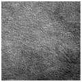
图2为实施例1制备的多晶硅薄膜的SEM图;Fig. 2 is the SEM image of the polysilicon film prepared in Example 1;
图3为实施例1制备的多晶硅薄膜的TEM图;3 is a TEM image of the polysilicon film prepared in Example 1;
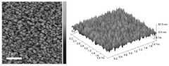
图4为实施例1制备的多晶硅薄膜的AFM测试结果;Fig. 4 is the AFM test result of the polysilicon film prepared in Example 1;
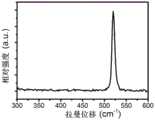
图5为实施例1制备的多晶硅薄膜的Raman测试结果;Fig. 5 is the Raman test result of the polysilicon film prepared in Example 1;
图6为实施例3制备的多晶硅薄膜的Raman测试结果。FIG. 6 is the Raman test result of the polysilicon thin film prepared in Example 3. FIG.
具体实施方式Detailed ways
为了使本发明的目的、技术方案及优点更加清楚明白,以下通过实施例并结合附图,对本发明进行进一步详细说明。In order to make the objectives, technical solutions and advantages of the present invention clearer, the present invention will be further described in detail below through embodiments and in conjunction with the accompanying drawings.
请参阅图1,本发明提供一种多晶硅薄膜的制备方法,包括以下步骤:Referring to FIG. 1, the present invention provides a method for preparing a polysilicon film, comprising the following steps:
S1,提供非晶硅薄膜,将所述非晶硅薄膜放入反应室中的水冷样品台上;S1, providing an amorphous silicon film, and placing the amorphous silicon film on a water-cooled sample stage in the reaction chamber;
S2,向所述反应室中通入等离子体气体源,并控制所述反应室的压力至100Pa至10000Pa;S2, feed the plasma gas source into the reaction chamber, and control the pressure of the reaction chamber to 100Pa to 10000Pa;
S3,激发所述等离子体气体源并产生等离子体,在所述等离子体环境中,所述非晶硅薄膜发生退火晶化,从而得到所述多晶硅薄膜。S3, the plasma gas source is excited to generate plasma, and in the plasma environment, the amorphous silicon thin film is annealed and crystallized, thereby obtaining the polycrystalline silicon thin film.
在步骤S1中,可进一步提供一衬底,用于支撑所述非晶硅薄膜。所述衬底可以是纯度较高的硅片,也可以是普通的石英玻璃。可以先在所述衬底上沉积所述非晶硅薄膜,然后将沉积有所述非晶硅薄膜的所述衬底放入所述反应室中。In step S1, a substrate may be further provided for supporting the amorphous silicon thin film. The substrate may be a silicon wafer with higher purity, or may be an ordinary quartz glass. The amorphous silicon thin film may be deposited on the substrate first, and then the substrate on which the amorphous silicon thin film is deposited is placed into the reaction chamber.
所述非晶硅薄膜的厚度可以是100nm~1μm,所述非晶硅薄膜过厚,所述等离子体对所述非晶硅薄膜的退火晶化效果变差,所述非晶硅薄膜过薄,容易被所述等离子体刻蚀掉。The thickness of the amorphous silicon film may be 100 nm to 1 μm. If the amorphous silicon film is too thick, the effect of the plasma on the annealing and crystallization of the amorphous silicon film becomes poor, and the amorphous silicon film is too thin. , easily etched away by the plasma.
在步骤S2之前,可进一步包括对所述反应室抽真空的步骤,以保证所述反应室内水蒸气和杂质气体的含量保持在较低水平。优选地,使所述反应室的本底真空度为10-3~10-6Pa。更为优选地,使所述反应室的本底真空度为10-5~10-6Pa。Before step S2, a step of vacuuming the reaction chamber may be further included to ensure that the content of water vapor and impurity gas in the reaction chamber is kept at a low level. Preferably, the background vacuum degree of the reaction chamber is 10-3 to 10-6 Pa. More preferably, the background vacuum degree of the reaction chamber is 10-5 to 10-6 Pa.
在步骤S2中,将所述反应室的压力调节至100Pa至10000Pa,可以在步骤S3中产生高能量的等离子体,高的等离子体能量能够使得非晶硅薄膜进行快速退火。另外,由于采用水冷样品台,可以保持衬底在比较低的温度条件下实现非晶硅薄膜的快速退火,衬底的低温条件可以使所述衬底的选择范围更宽,即使所述衬底(例如廉价的玻璃)的纯度不高,所述衬底中的杂质也不会发生高温扩散,这样大大降低了所述多晶硅薄膜的制备成本,更有利于其产业化。In step S2, the pressure of the reaction chamber is adjusted to 100Pa to 10000Pa, high-energy plasma can be generated in step S3, and the high plasma energy can make the amorphous silicon thin film perform rapid annealing. In addition, due to the use of the water-cooled sample stage, the substrate can be kept at a relatively low temperature to achieve rapid annealing of the amorphous silicon film. The purity of (eg, cheap glass) is not high, and impurities in the substrate will not diffuse at high temperature, which greatly reduces the preparation cost of the polysilicon film and is more conducive to its industrialization.
优选地,可将所述反应室的压力调节至200-1500Pa。更为优选地,可将所述反应室的压力调节至500-1000Pa。Preferably, the pressure of the reaction chamber can be adjusted to 200-1500Pa. More preferably, the pressure of the reaction chamber can be adjusted to 500-1000Pa.
优选地,所述非晶硅薄膜退火晶化过程中,所述衬底的温度为300-700℃。更为优选地,所述非晶硅薄膜退火晶化过程中,所述衬底的温度为400-600℃。Preferably, during the annealing and crystallization process of the amorphous silicon thin film, the temperature of the substrate is 300-700°C. More preferably, during the annealing and crystallization process of the amorphous silicon thin film, the temperature of the substrate is 400-600°C.
所述等离子体气体源用于产生等离子体且不与所述非晶硅薄膜和多晶硅薄膜发生化学反应。所述等离子体气体源可以包括氩气和/或氦气中的至少一种。所述等离子体气体源的通入流量可以为10~30slm。优选地,所述等离子体气体源的通入流量可以为15-25slm。The plasma gas source is used to generate plasma and does not chemically react with the amorphous silicon thin film and the polysilicon thin film. The plasma gas source may include at least one of argon and/or helium. The incoming flow rate of the plasma gas source may be 10-30 slm. Preferably, the incoming flow rate of the plasma gas source may be 15-25 slm.
所述等离子体气体源可进一步包括氢气。所述氢气在所述步骤S3中会分解为H原子,H原子对所述非晶硅薄膜的晶化有促进作用,从而进一步缩短所述多晶硅薄膜的制备时间。优选地,所述氢气的通入流量不超过1.0slm,更为优选地,所述氢气的通入流量为0.3~0.7slm。The plasma gas source may further include hydrogen gas. The hydrogen gas will be decomposed into H atoms in the step S3, and the H atoms can promote the crystallization of the amorphous silicon thin film, thereby further shortening the preparation time of the polycrystalline silicon thin film. Preferably, the inflow rate of the hydrogen does not exceed 1.0 slm, and more preferably, the inflow rate of the hydrogen is 0.3-0.7 slm.
在步骤S3中,可以采用射频电源对所述反应室施加一射频电场,从而激发所述等离子体气体源产生所述等离子体。可以采用电感耦合或直流电弧方式通过等离子体喷枪产生等离子体。In step S3, a radio frequency electric field may be applied to the reaction chamber by a radio frequency power source, so as to excite the plasma gas source to generate the plasma. Plasma can be generated through a plasma torch using inductive coupling or DC arcing.
所述等离子体喷枪的直径可以为40-60mm,所述非晶硅薄膜与所述等离子体喷枪出口的距离可以为20-60mm。优选地,所述射频电源的功率设置为10~20kw,所述射频电源的功率越大,所述非晶硅薄膜的晶化时间越短,然而,若所述射频电源的功率过大,则会使所述非晶硅薄膜发生刻蚀情况,从而不能得到完整的多晶硅薄膜。更为优选地,所述射频电源的功率设置为12~16kw。The diameter of the plasma torch may be 40-60 mm, and the distance between the amorphous silicon film and the outlet of the plasma torch may be 20-60 mm. Preferably, the power of the radio frequency power supply is set to 10-20kw. The greater the power of the radio frequency power supply, the shorter the crystallization time of the amorphous silicon film. However, if the power of the radio frequency power supply is too large, the The amorphous silicon film will be etched, so that a complete polysilicon film cannot be obtained. More preferably, the power of the radio frequency power supply is set to 12-16kw.
优选地,所述非晶硅薄膜退火晶化所需的时间为5-30s。更为优选地,所述非晶硅薄膜退火晶化所需的时间为5-15s。Preferably, the time required for annealing and crystallization of the amorphous silicon film is 5-30s. More preferably, the time required for the annealing and crystallization of the amorphous silicon film is 5-15s.
本发明中快速退火晶化的原理为:上述等离子体环境中,等离子体气体的温度超过2000℃,并且在优化的条件下具有非常高的H原子浓度。高的等离子体能量能够使得非晶硅薄膜进行快速退火;由于采用水冷样品台,可以保持衬底在比较低的温度条件下实现非晶硅膜层的快速退火。另外,由于在上述等离子体环境中存在大量的原子态的H,由于H原子的化学退火作用,大量H原子的存在能够进一步促进非晶硅薄膜的退火晶化。综合上述两方面原因,可以实现非晶硅薄膜的快速退火;另外,由于退火时间比较短,衬底本身被加热后的温度不会很高,加上水冷样品台的使用,可以把衬底温度控制在比较低的水平。The principle of rapid annealing and crystallization in the present invention is that in the above-mentioned plasma environment, the temperature of the plasma gas exceeds 2000° C., and under optimized conditions, the plasma gas has a very high concentration of H atoms. High plasma energy enables rapid annealing of the amorphous silicon film; due to the use of a water-cooled sample stage, the substrate can be maintained at a relatively low temperature to achieve rapid annealing of the amorphous silicon film. In addition, since a large amount of atomic H exists in the above-mentioned plasma environment, the presence of a large amount of H atoms can further promote the annealing crystallization of the amorphous silicon thin film due to the chemical annealing effect of the H atoms. Combining the above two reasons, rapid annealing of amorphous silicon films can be achieved; in addition, due to the relatively short annealing time, the temperature of the substrate itself after being heated will not be very high, and the use of a water-cooled sample stage can reduce the substrate temperature. controlled at a relatively low level.
本发明还可以通过控制所述压力、射频电源功率、退火时间、氢气的流量等等因素来得到不同晶化程度的微晶硅薄膜、多晶硅薄膜或其组合。The present invention can also obtain microcrystalline silicon films, polycrystalline silicon films or combinations thereof with different degrees of crystallization by controlling the pressure, radio frequency power supply, annealing time, hydrogen flow and other factors.
本发明进一步提供一种光电器件,包括采用上述制备方法制备的多晶硅薄膜。The present invention further provides an optoelectronic device, comprising the polysilicon film prepared by the above preparation method.
实施例1Example 1
在清洗过的3cm×3cm硅片衬底上沉积一层1μm厚的非晶硅薄膜,取出样品并将其安装在中压等离子CVD设备的水冷样品台上,调节样品台高度,使衬底表面与等离子体喷枪出口距离在30mm,关上真空腔室并且将真空室抽至10-5Pa的本底真空度,关闭连接分子泵组与腔体之间的闸板阀并打开工艺泵组和压力控制阀,通入流量为20slm的高纯Ar,并且通过调节压力控制阀使真空室内的压力达到800Pa,通入流量为0.5slm的高纯H2并打开射频电源,产生等离子体,调节射频电源功率至14kW,退火温度为552℃,退火时间为7s。退火结束后关闭H2、关闭等离子体电源、关闭Ar。A layer of 1μm thick amorphous silicon film was deposited on the cleaned 3cm×3cm silicon wafer substrate, the sample was taken out and installed on the water-cooled sample stage of the medium pressure plasma CVD equipment, and the height of the sample stage was adjusted so that the substrate surface The distance from the plasma spray gun outlet is 30mm, close the vacuum chamber and pump the vacuum chamber to a background vacuum of 10-5 Pa, close the gate valve connecting the molecular pump set and the chamber, and open the process pump set and pressure Control valve, pass high-purity Ar with a flow rate of 20slm, and adjust the pressure control valve to make the pressure in the vacuum chamber reach 800Pa, pass in high-purityH2 with a flow rate of 0.5slm and turn on the radio frequency power supply, generate plasma, and adjust the radio frequency power supply The power was 14kW, the annealing temperature was 552°C, and the annealing time was 7s. After annealing, turn off H2 , turn off the plasma power supply, and turn off Ar.
实施例2Example 2
本实施例与实施例1基本相同,不同之处在于,衬底为石英玻璃衬底,等离子体气体源为Ar与H2的混合气体,等离子体气体源的流量为10slm,反应室的腔体压力为200Pa,退火功率为16kW,退火时间为5s,退火温度为600℃。This embodiment is basically the same as Embodiment 1, except that the substrate is a quartz glass substrate, the plasma gas source is a mixed gas of Ar and H2 , the flow rate of the plasma gas source is 10slm, and the cavity of the reaction chamber is The pressure is 200Pa, the annealing power is 16kW, the annealing time is 5s, and the annealing temperature is 600℃.
实施例3Example 3
本实施例与实施例1基本相同,不同之处在于,等离子体气体源为He与H2的混合气体,等离子体气体源的流量为30slm,薄膜厚度为200nm,退火时间为10s,退火温度为500℃。This embodiment is basically the same as Embodiment 1, except that the plasma gas source is a mixed gas of He and H2 , the flow rate of the plasma gas source is 30slm, the film thickness is 200nm, the annealing time is 10s, and the annealing temperature is 500°C.
实施例4Example 4
本实施例与实施例1基本相同,不同之处在于,等离子体气体源为He,等离子体气体源的流量为15slm,薄膜厚度为500nm,腔体压力调节为1500Pa,衬底表面与等离子体喷枪出口的距离为40mm,退火功率为18kW,H2流量为0.3slm,退火时间为8s,退火温度为700℃。This embodiment is basically the same as Embodiment 1, except that the plasma gas source is He, the flow rate of the plasma gas source is 15slm, the film thickness is 500nm, the cavity pressure is adjusted to 1500Pa, the surface of the substrate and the plasma spray gun are adjusted to The distance of the outlet is 40mm, the annealing power is 18kW, theH2 flow rate is 0.3slm, the annealing time is 8s, and the annealing temperature is 700°C.
实施例5Example 5
本实施例与实施例1基本相同,不同之处在于,所用衬底为5cm×5cm硅片,等离子体气体源为Ar与H2的混合气体,等离子体气体源的流量为25slm,腔体压力调节为400Pa,衬底表面与等离子体喷枪出口的距离为20mm,射频电源功率为16kW,H2流量为0.7slm,退火时间为10s,退火温度为643℃。This embodiment is basically the same as Embodiment 1, except that the substrate used is a 5cm×5cm silicon wafer, the plasma gas source is a mixed gas of Ar and H2 , the flow rate of the plasma gas source is 25slm, and the chamber pressure is Adjusted to 400 Pa, the distance between the substrate surface and the plasma torch outlet was 20 mm, the RF power was16 kW, the H flow was 0.7 slm, the annealing time was 10 s, and the annealing temperature was 643 °C.
实施例6Example 6
本实施例与实施例5基本相同,不同之处在于,仅通入21slm的高纯Ar而并不通入H2,衬底表面与等离子体喷枪出口的距离为60mm,射频电源功率为15kW,退火时间为15s,退火温度为593℃。This example is basically the same as Example 5, the difference is that only 21 slm of high-purity Ar is passed in instead of H2 , the distance between the substrate surface and the outlet of the plasma torch is 60 mm, the power of the radio frequency power is 15 kW, and the annealing is performed. The time was 15s, and the annealing temperature was 593°C.
实施例7Example 7
本实施例与实施例1基本相同,不同之处在于,等离子体气体源为Ar与H2的混合气体,等离子体气体的流量为30slm,腔体压力为1000Pa,H2流量为0.4slm,退火时间为25s,退火温度为800℃。This embodiment is basically the same as Embodiment 1, except that the plasma gas source is a mixed gas of Ar and H2 , the flow rate of the plasma gas is 30slm, the cavity pressure is 1000Pa, the flow rate of H2 is 0.4slm, and the annealing The time was 25 s, and the annealing temperature was 800 °C.
表1Table 1

请参阅图2至图4,从图中可以看出,由本发明提供的制备方法得到的多晶硅薄膜具有明显的晶粒结构,表明所述非晶硅薄膜发生了晶化,所述多晶硅薄膜的表面粗糙度Ra为4.35nm。图5中峰值位于480cm-1、510cm-1、520cm-1分别代表非晶组分、多晶组分以及单晶组分,从图5可以看出,所述多晶硅薄膜的晶化程度很高;而图6的晶化程度则达到了100%。表1为实施例1至7制备的多晶硅薄膜的晶化程度表,从表1可以看出,本发明在30s内即可得到完全晶化的多晶硅薄膜,而且所述非晶硅薄膜的退火温度很低。此外,氢气对所述非晶硅薄膜的晶化具有促进作用,且在0.3~0.7sml的流量条件下,其促进作用最强。Please refer to FIG. 2 to FIG. 4. It can be seen from the figures that the polysilicon film obtained by the preparation method provided by the present invention has an obvious grain structure, indicating that the amorphous silicon film is crystallized, and the surface of the polysilicon film is The roughness Ra was 4.35 nm. The peaks located at 480cm-1 , 510cm-1 and 520cm-1 in Fig. 5 represent the amorphous component, the polycrystalline component and the single crystal component, respectively. It can be seen from Fig. 5 that the polycrystalline silicon film has a high degree of crystallization ; while the degree of crystallization in Figure 6 reached 100%. Table 1 is a table of the crystallization degree of the polysilicon films prepared in Examples 1 to 7. It can be seen from Table 1 that the present invention can obtain a fully crystallized polysilicon film within 30s, and the annealing temperature of the amorphous silicon film very low. In addition, hydrogen has a promoting effect on the crystallization of the amorphous silicon thin film, and under the condition of a flow rate of 0.3-0.7 sml, its promoting effect is the strongest.
本发明提供的多晶硅薄膜制备工艺,通过将非晶硅薄膜置于中压条件下电感耦合产生的射频等离子体环境中,从而使非晶硅薄膜快速晶化,且在低温条件下即可快速获得多晶硅薄膜,不仅可以使用普通玻璃等廉价衬底,极大的降低了制备成本,而且极大的节约了时间成本,同时还具有低沉本、大面积制备和工艺简单的优势。The polycrystalline silicon thin film preparation process provided by the present invention can rapidly crystallize the amorphous silicon thin film by placing the amorphous silicon thin film in a radio frequency plasma environment generated by inductive coupling under medium voltage conditions, and can be quickly obtained under low temperature conditions Polysilicon thin films can not only use cheap substrates such as ordinary glass, which greatly reduces the preparation cost, but also greatly saves time and cost, and also has the advantages of low cost, large area preparation and simple process.
以上所述实施例的各技术特征可以进行任意的组合,为使描述简洁,未对上述实施例中的各个技术特征所有可能的组合都进行描述,然而,只要这些技术特征的组合不存在矛盾,都应当认为是本说明书记载的范围。The technical features of the above-described embodiments can be combined arbitrarily. For the sake of brevity, all possible combinations of the technical features in the above-described embodiments are not described. However, as long as there is no contradiction between the combinations of these technical features, All should be regarded as the scope described in this specification.
以上所述实施例仅表达了本发明的几种实施方式,其描述较为具体和详细,但并不能因此而理解为对发明专利范围的限制。应当指出的是,对于本领域的普通技术人员来说,在不脱离本发明构思的前提下,还可以做出若干变形和改进,这些都属于本发明的保护范围。因此,本发明专利的保护范围应以所附权利要求为准。The above-mentioned embodiments only represent several embodiments of the present invention, and the descriptions thereof are specific and detailed, but should not be construed as a limitation on the scope of the invention patent. It should be pointed out that for those of ordinary skill in the art, without departing from the concept of the present invention, several modifications and improvements can also be made, which all belong to the protection scope of the present invention. Therefore, the protection scope of the patent of the present invention should be subject to the appended claims.
Claims (8)
Translated fromChinesePriority Applications (1)
| Application Number | Priority Date | Filing Date | Title |
|---|---|---|---|
| CN201611227126.8ACN106653572B (en) | 2016-12-27 | 2016-12-27 | Preparation method of polysilicon thin film and optoelectronic device |
Applications Claiming Priority (1)
| Application Number | Priority Date | Filing Date | Title |
|---|---|---|---|
| CN201611227126.8ACN106653572B (en) | 2016-12-27 | 2016-12-27 | Preparation method of polysilicon thin film and optoelectronic device |
Publications (2)
| Publication Number | Publication Date |
|---|---|
| CN106653572A CN106653572A (en) | 2017-05-10 |
| CN106653572Btrue CN106653572B (en) | 2020-01-17 |
Family
ID=58831462
Family Applications (1)
| Application Number | Title | Priority Date | Filing Date |
|---|---|---|---|
| CN201611227126.8AActiveCN106653572B (en) | 2016-12-27 | 2016-12-27 | Preparation method of polysilicon thin film and optoelectronic device |
Country Status (1)
| Country | Link |
|---|---|
| CN (1) | CN106653572B (en) |
Families Citing this family (2)
| Publication number | Priority date | Publication date | Assignee | Title |
|---|---|---|---|---|
| CN110760925A (en)* | 2019-11-15 | 2020-02-07 | 常州时创能源科技有限公司 | Method for depositing amorphous silicon thin film by PECVD and application thereof |
| CN114864751B (en)* | 2022-05-19 | 2023-07-07 | 通威太阳能(眉山)有限公司 | Solar cell and its preparation method |
Citations (2)
| Publication number | Priority date | Publication date | Assignee | Title |
|---|---|---|---|---|
| CN102103989A (en)* | 2009-12-18 | 2011-06-22 | 华映视讯(吴江)有限公司 | Method for forming crystalline silicon thin film |
| CN104822219A (en)* | 2015-05-18 | 2015-08-05 | 京东方科技集团股份有限公司 | Plasma generator, annealing equipment, coating crystallization equipment, and annealing process |
Family Cites Families (2)
| Publication number | Priority date | Publication date | Assignee | Title |
|---|---|---|---|---|
| TWI514347B (en)* | 2006-09-29 | 2015-12-21 | Semiconductor Energy Lab | Display device and electronic device |
| CN101414564B (en)* | 2008-11-24 | 2010-07-14 | 上海广电光电子有限公司 | Method for manufacturing low-temperature polycrystalline silicon film transistor |
- 2016
- 2016-12-27CNCN201611227126.8Apatent/CN106653572B/enactiveActive
Patent Citations (2)
| Publication number | Priority date | Publication date | Assignee | Title |
|---|---|---|---|---|
| CN102103989A (en)* | 2009-12-18 | 2011-06-22 | 华映视讯(吴江)有限公司 | Method for forming crystalline silicon thin film |
| CN104822219A (en)* | 2015-05-18 | 2015-08-05 | 京东方科技集团股份有限公司 | Plasma generator, annealing equipment, coating crystallization equipment, and annealing process |
Also Published As
| Publication number | Publication date |
|---|---|
| CN106653572A (en) | 2017-05-10 |
Similar Documents
| Publication | Publication Date | Title |
|---|---|---|
| TWI393191B (en) | Low temperature thin film transistor process, device characteristics, and device stability improvement | |
| KR100797018B1 (en) | Semiconductor thin film, semiconductor device using same, manufacturing method thereof and apparatus for manufacturing semiconductor thin film | |
| CN102849733B (en) | Low-temperature direct preparation method of graphene under double-temperature-zone control, and double-temperature-zone tube furnace | |
| WO2020168819A1 (en) | Method for efficiently eliminating graphene wrinkles formed by chemical vapor deposition | |
| JP2008124111A (en) | Method for forming silicon-based thin film by plasma CVD method | |
| JPH08973B2 (en) | Deposited film formation method | |
| CN101665905A (en) | Aluminum-induced low temperature preparation method of large grain size polysilicon film | |
| US7186663B2 (en) | High density plasma process for silicon thin films | |
| CN110228806A (en) | The method for preparing graphene film using plasma reinforced chemical vapour deposition method | |
| CN101724901A (en) | Method for preparing aluminum-induced crystallized polycrystalline silicon film in hydrogen plasma atmosphere | |
| CN106653572B (en) | Preparation method of polysilicon thin film and optoelectronic device | |
| TWI291206B (en) | Method of direct deposition of polycrystalline silicon | |
| CN111826712A (en) | A method for preparing wafer-level uniform hexagonal boron nitride thin film | |
| CN102709404A (en) | Method for preparing polycrystalline silicon film by carrying out induced crystallization on amorphous silicon film by using metallic copper under low temperature | |
| CN111910171A (en) | A device and method for controlling and synthesizing two-dimensional materials by electric field and/or magnetic field | |
| JP2002110551A (en) | Method and apparatus for forming semiconductor thin film | |
| CN1727525A (en) | A method for preparing polysilicon | |
| JPS62228471A (en) | Deposited film formation method | |
| KR101564331B1 (en) | Hot-wire chemical vapor deposition apparatus equipped with electric field control device and thin film manufacturing method using the same | |
| TWI377173B (en) | Method for manufacturing crystalline silicon | |
| CN111519186A (en) | Ferromagnetic/graphene epitaxial interface and low-temperature preparation method thereof | |
| CN101487114B (en) | Low-temperature polycrystalline silicon thin film device and manufacturing method thereof | |
| CN100537838C (en) | Low-temperature polycrystalline silicon thin film device and manufacturing method and equipment thereof | |
| CN103311105A (en) | Method for inducing crystallization of amorphous silicon thin film into polycrystalline silicon thin film by aluminum at low temperature | |
| RU2769751C1 (en) | Device for deposition of ultra-thick layers of polycrystalline silicon |
Legal Events
| Date | Code | Title | Description |
|---|---|---|---|
| PB01 | Publication | ||
| PB01 | Publication | ||
| SE01 | Entry into force of request for substantive examination | ||
| SE01 | Entry into force of request for substantive examination | ||
| GR01 | Patent grant | ||
| GR01 | Patent grant |