CN106558493B - Method for forming fin field effect transistor - Google Patents
Method for forming fin field effect transistorDownload PDFInfo
- Publication number
- CN106558493B CN106558493BCN201510631671.2ACN201510631671ACN106558493BCN 106558493 BCN106558493 BCN 106558493BCN 201510631671 ACN201510631671 ACN 201510631671ACN 106558493 BCN106558493 BCN 106558493B
- Authority
- CN
- China
- Prior art keywords
- layer
- region
- ions
- forming
- hole
- Prior art date
- Legal status (The legal status is an assumption and is not a legal conclusion. Google has not performed a legal analysis and makes no representation as to the accuracy of the status listed.)
- Active
Links
- 238000000034methodMethods0.000titleclaimsabstractdescription126
- 230000005669field effectEffects0.000titleclaimsabstractdescription36
- 150000002500ionsChemical class0.000claimsabstractdescription117
- 229910003460diamondInorganic materials0.000claimsabstractdescription81
- 239000010432diamondSubstances0.000claimsabstractdescription81
- 239000000758substrateSubstances0.000claimsabstractdescription78
- 238000005530etchingMethods0.000claimsabstractdescription23
- 230000008569processEffects0.000claimsdescription89
- 239000000463materialSubstances0.000claimsdescription84
- 230000002265preventionEffects0.000claimsdescription29
- XUIMIQQOPSSXEZ-UHFFFAOYSA-NSiliconChemical compound[Si]XUIMIQQOPSSXEZ-UHFFFAOYSA-N0.000claimsdescription27
- 229910052710siliconInorganic materials0.000claimsdescription27
- 239000010703siliconSubstances0.000claimsdescription27
- -1boron ionsChemical class0.000claimsdescription17
- VYPSYNLAJGMNEJ-UHFFFAOYSA-NSilicium dioxideChemical compoundO=[Si]=OVYPSYNLAJGMNEJ-UHFFFAOYSA-N0.000claimsdescription14
- 229910052814silicon oxideInorganic materials0.000claimsdescription14
- 229910000577Silicon-germaniumInorganic materials0.000claimsdescription10
- 150000001875compoundsChemical class0.000claimsdescription10
- HBMJWWWQQXIZIP-UHFFFAOYSA-Nsilicon carbideChemical compound[Si+]#[C-]HBMJWWWQQXIZIP-UHFFFAOYSA-N0.000claimsdescription10
- 229910010271silicon carbideInorganic materials0.000claimsdescription10
- LEVVHYCKPQWKOP-UHFFFAOYSA-N[Si].[Ge]Chemical compound[Si].[Ge]LEVVHYCKPQWKOP-UHFFFAOYSA-N0.000claimsdescription9
- 229910052732germaniumInorganic materials0.000claimsdescription9
- GNPVGFCGXDBREM-UHFFFAOYSA-Ngermanium atomChemical compound[Ge]GNPVGFCGXDBREM-UHFFFAOYSA-N0.000claimsdescription9
- 229910052796boronInorganic materials0.000claimsdescription8
- 238000010438heat treatmentMethods0.000claimsdescription7
- 229910000530Gallium indium arsenideInorganic materials0.000claimsdescription6
- 229910052581Si3N4Inorganic materials0.000claimsdescription6
- 238000001312dry etchingMethods0.000claimsdescription6
- HQVNEWCFYHHQES-UHFFFAOYSA-Nsilicon nitrideChemical compoundN12[Si]34N5[Si]62N3[Si]51N64HQVNEWCFYHHQES-UHFFFAOYSA-N0.000claimsdescription6
- JBRZTFJDHDCESZ-UHFFFAOYSA-NAsGaChemical compound[As]#[Ga]JBRZTFJDHDCESZ-UHFFFAOYSA-N0.000claimsdescription5
- OKTJSMMVPCPJKN-UHFFFAOYSA-NCarbonChemical compound[C]OKTJSMMVPCPJKN-UHFFFAOYSA-N0.000claimsdescription5
- 239000004215Carbon black (E152)Substances0.000claimsdescription5
- 229910001218Gallium arsenideInorganic materials0.000claimsdescription5
- 229910052799carbonInorganic materials0.000claimsdescription5
- 229930195733hydrocarbonNatural products0.000claimsdescription5
- 150000002430hydrocarbonsChemical class0.000claimsdescription5
- RPQDHPTXJYYUPQ-UHFFFAOYSA-Nindium arsenideChemical compound[In]#[As]RPQDHPTXJYYUPQ-UHFFFAOYSA-N0.000claimsdescription5
- 229910000673Indium arsenideInorganic materials0.000claimsdescription4
- WPYVAWXEWQSOGY-UHFFFAOYSA-Nindium antimonideChemical compound[Sb]#[In]WPYVAWXEWQSOGY-UHFFFAOYSA-N0.000claimsdescription4
- 230000036961partial effectEffects0.000abstractdescription8
- 239000010410layerSubstances0.000description357
- 239000010408filmSubstances0.000description46
- 239000002019doping agentSubstances0.000description13
- 239000007789gasSubstances0.000description12
- 238000005468ion implantationMethods0.000description12
- 238000000407epitaxyMethods0.000description11
- 238000010586diagramMethods0.000description9
- 229920002120photoresistant polymerPolymers0.000description9
- 239000010409thin filmSubstances0.000description9
- 238000011065in-situ storageMethods0.000description8
- 230000000694effectsEffects0.000description7
- 239000011229interlayerSubstances0.000description7
- 238000002955isolationMethods0.000description7
- 229910052698phosphorusInorganic materials0.000description7
- 239000011574phosphorusSubstances0.000description7
- 238000001039wet etchingMethods0.000description7
- 230000002411adverseEffects0.000description6
- 230000015572biosynthetic processEffects0.000description6
- 229910021420polycrystalline siliconInorganic materials0.000description6
- 229920005591polysiliconPolymers0.000description6
- 238000009826distributionMethods0.000description5
- 230000003647oxidationEffects0.000description5
- 238000007254oxidation reactionMethods0.000description5
- 239000004065semiconductorSubstances0.000description5
- 230000002441reversible effectEffects0.000description4
- 230000007547defectEffects0.000description3
- 239000003989dielectric materialSubstances0.000description3
- 229910052733galliumInorganic materials0.000description3
- 238000002513implantationMethods0.000description3
- RYGMFSIKBFXOCR-UHFFFAOYSA-NCopperChemical compound[Cu]RYGMFSIKBFXOCR-UHFFFAOYSA-N0.000description2
- KRHYYFGTRYWZRS-UHFFFAOYSA-NFluoraneChemical compoundFKRHYYFGTRYWZRS-UHFFFAOYSA-N0.000description2
- GYHNNYVSQQEPJS-UHFFFAOYSA-NGalliumChemical compound[Ga]GYHNNYVSQQEPJS-UHFFFAOYSA-N0.000description2
- BQCADISMDOOEFD-UHFFFAOYSA-NSilverChemical compound[Ag]BQCADISMDOOEFD-UHFFFAOYSA-N0.000description2
- NRTOMJZYCJJWKI-UHFFFAOYSA-NTitanium nitrideChemical compound[Ti]#NNRTOMJZYCJJWKI-UHFFFAOYSA-N0.000description2
- 229910052782aluminiumInorganic materials0.000description2
- XAGFODPZIPBFFR-UHFFFAOYSA-NaluminiumChemical compound[Al]XAGFODPZIPBFFR-UHFFFAOYSA-N0.000description2
- 238000000231atomic layer depositionMethods0.000description2
- 238000005229chemical vapour depositionMethods0.000description2
- 229910052802copperInorganic materials0.000description2
- 239000010949copperSubstances0.000description2
- 238000005137deposition processMethods0.000description2
- 238000011161developmentMethods0.000description2
- 238000009792diffusion processMethods0.000description2
- 238000005516engineering processMethods0.000description2
- PCHJSUWPFVWCPO-UHFFFAOYSA-NgoldChemical compound[Au]PCHJSUWPFVWCPO-UHFFFAOYSA-N0.000description2
- 229910052737goldInorganic materials0.000description2
- 239000010931goldSubstances0.000description2
- 238000000227grindingMethods0.000description2
- 239000012212insulatorSubstances0.000description2
- MRELNEQAGSRDBK-UHFFFAOYSA-Nlanthanum(3+);oxygen(2-)Chemical compound[O-2].[O-2].[O-2].[La+3].[La+3]MRELNEQAGSRDBK-UHFFFAOYSA-N0.000description2
- 238000004519manufacturing processMethods0.000description2
- VNWKTOKETHGBQD-UHFFFAOYSA-NmethaneChemical compoundCVNWKTOKETHGBQD-UHFFFAOYSA-N0.000description2
- 230000035515penetrationEffects0.000description2
- 238000005240physical vapour depositionMethods0.000description2
- 230000002829reductive effectEffects0.000description2
- 238000004904shorteningMethods0.000description2
- 229910052709silverInorganic materials0.000description2
- 239000004332silverSubstances0.000description2
- MZLGASXMSKOWSE-UHFFFAOYSA-Ntantalum nitrideChemical compound[Ta]#NMZLGASXMSKOWSE-UHFFFAOYSA-N0.000description2
- WFKWXMTUELFFGS-UHFFFAOYSA-NtungstenChemical compound[W]WFKWXMTUELFFGS-UHFFFAOYSA-N0.000description2
- 229910052721tungstenInorganic materials0.000description2
- 239000010937tungstenSubstances0.000description2
- ZOXJGFHDIHLPTG-UHFFFAOYSA-NBoronChemical compound[B]ZOXJGFHDIHLPTG-UHFFFAOYSA-N0.000description1
- OAICVXFJPJFONN-UHFFFAOYSA-NPhosphorusChemical compound[P]OAICVXFJPJFONN-UHFFFAOYSA-N0.000description1
- GWEVSGVZZGPLCZ-UHFFFAOYSA-NTitan oxideChemical compoundO=[Ti]=OGWEVSGVZZGPLCZ-UHFFFAOYSA-N0.000description1
- FAUIDPFKEVQLLR-UHFFFAOYSA-N[O-2].[Zr+4].[Si+4].[O-2].[O-2].[O-2]Chemical compound[O-2].[Zr+4].[Si+4].[O-2].[O-2].[O-2]FAUIDPFKEVQLLR-UHFFFAOYSA-N0.000description1
- ILCYGSITMBHYNK-UHFFFAOYSA-N[Si]=O.[Hf]Chemical compound[Si]=O.[Hf]ILCYGSITMBHYNK-UHFFFAOYSA-N0.000description1
- HSFWRNGVRCDJHI-UHFFFAOYSA-Nalpha-acetyleneNatural productsC#CHSFWRNGVRCDJHI-UHFFFAOYSA-N0.000description1
- 229910001439antimony ionInorganic materials0.000description1
- HAYXDMNJJFVXCI-UHFFFAOYSA-Narsenic(5+)Chemical compound[As+5]HAYXDMNJJFVXCI-UHFFFAOYSA-N0.000description1
- 238000004380ashingMethods0.000description1
- VKJLWXGJGDEGSO-UHFFFAOYSA-Nbarium(2+);oxygen(2-);titanium(4+)Chemical compound[O-2].[O-2].[O-2].[Ti+4].[Ba+2]VKJLWXGJGDEGSO-UHFFFAOYSA-N0.000description1
- 230000008859changeEffects0.000description1
- 238000006243chemical reactionMethods0.000description1
- 238000004140cleaningMethods0.000description1
- 239000013078crystalSubstances0.000description1
- 230000003247decreasing effectEffects0.000description1
- 230000005684electric fieldEffects0.000description1
- 125000002534ethynyl groupChemical group[H]C#C*0.000description1
- 229910000449hafnium oxideInorganic materials0.000description1
- WIHZLLGSGQNAGK-UHFFFAOYSA-Nhafnium(4+);oxygen(2-)Chemical compound[O-2].[O-2].[Hf+4]WIHZLLGSGQNAGK-UHFFFAOYSA-N0.000description1
- 230000036039immunityEffects0.000description1
- 229910052738indiumInorganic materials0.000description1
- APFVFJFRJDLVQX-UHFFFAOYSA-Nindium atomChemical compound[In]APFVFJFRJDLVQX-UHFFFAOYSA-N0.000description1
- 229910001449indium ionInorganic materials0.000description1
- 239000007788liquidSubstances0.000description1
- 238000012986modificationMethods0.000description1
- 230000004048modificationEffects0.000description1
- 231100000989no adverse effectToxicity0.000description1
- TWNQGVIAIRXVLR-UHFFFAOYSA-Noxo(oxoalumanyloxy)alumaneChemical compoundO=[Al]O[Al]=OTWNQGVIAIRXVLR-UHFFFAOYSA-N0.000description1
- BPUBBGLMJRNUCC-UHFFFAOYSA-Noxygen(2-);tantalum(5+)Chemical compound[O-2].[O-2].[O-2].[O-2].[O-2].[Ta+5].[Ta+5]BPUBBGLMJRNUCC-UHFFFAOYSA-N0.000description1
- RVTZCBVAJQQJTK-UHFFFAOYSA-Noxygen(2-);zirconium(4+)Chemical compound[O-2].[O-2].[Zr+4]RVTZCBVAJQQJTK-UHFFFAOYSA-N0.000description1
- 238000007517polishing processMethods0.000description1
- 230000009467reductionEffects0.000description1
- 238000011160researchMethods0.000description1
- VEALVRVVWBQVSL-UHFFFAOYSA-Nstrontium titanateChemical compound[Sr+2].[O-][Ti]([O-])=OVEALVRVVWBQVSL-UHFFFAOYSA-N0.000description1
- CZXRMHUWVGPWRM-UHFFFAOYSA-Nstrontium;barium(2+);oxygen(2-);titanium(4+)Chemical compound[O-2].[O-2].[O-2].[O-2].[Ti+4].[Sr+2].[Ba+2]CZXRMHUWVGPWRM-UHFFFAOYSA-N0.000description1
- 239000000126substanceSubstances0.000description1
- 229910001936tantalum oxideInorganic materials0.000description1
- OGIDPMRJRNCKJF-UHFFFAOYSA-Ntitanium oxideInorganic materials[Ti]=OOGIDPMRJRNCKJF-UHFFFAOYSA-N0.000description1
- 238000012546transferMethods0.000description1
- 230000007704transitionEffects0.000description1
- 229910001928zirconium oxideInorganic materials0.000description1
Images


Classifications
- H—ELECTRICITY
- H10—SEMICONDUCTOR DEVICES; ELECTRIC SOLID-STATE DEVICES NOT OTHERWISE PROVIDED FOR
- H10D—INORGANIC ELECTRIC SEMICONDUCTOR DEVICES
- H10D30/00—Field-effect transistors [FET]
- H10D30/01—Manufacture or treatment
- H10D30/021—Manufacture or treatment of FETs having insulated gates [IGFET]
- H10D30/024—Manufacture or treatment of FETs having insulated gates [IGFET] of fin field-effect transistors [FinFET]
- H—ELECTRICITY
- H01—ELECTRIC ELEMENTS
- H01L—SEMICONDUCTOR DEVICES NOT COVERED BY CLASS H10
- H01L21/00—Processes or apparatus adapted for the manufacture or treatment of semiconductor or solid state devices or of parts thereof
- H01L21/70—Manufacture or treatment of devices consisting of a plurality of solid state components formed in or on a common substrate or of parts thereof; Manufacture of integrated circuit devices or of parts thereof
- H01L21/71—Manufacture of specific parts of devices defined in group H01L21/70
- H01L21/76—Making of isolation regions between components
- H—ELECTRICITY
- H10—SEMICONDUCTOR DEVICES; ELECTRIC SOLID-STATE DEVICES NOT OTHERWISE PROVIDED FOR
- H10D—INORGANIC ELECTRIC SEMICONDUCTOR DEVICES
- H10D62/00—Semiconductor bodies, or regions thereof, of devices having potential barriers
- H10D62/10—Shapes, relative sizes or dispositions of the regions of the semiconductor bodies; Shapes of the semiconductor bodies
Landscapes
- Engineering & Computer Science (AREA)
- Physics & Mathematics (AREA)
- Condensed Matter Physics & Semiconductors (AREA)
- General Physics & Mathematics (AREA)
- Manufacturing & Machinery (AREA)
- Computer Hardware Design (AREA)
- Microelectronics & Electronic Packaging (AREA)
- Power Engineering (AREA)
- Insulated Gate Type Field-Effect Transistor (AREA)
Abstract
Translated fromChinese
Description
Translated fromChinese技术领域technical field
本发明涉及半导体制造技术领域,特别涉及一种鳍式场效应管的形成方法。The present invention relates to the technical field of semiconductor manufacturing, in particular to a method for forming a fin field effect transistor.
背景技术Background technique
随着半导体工艺技术的不断发展,半导体工艺节点遵循摩尔定律的发展趋势不断减小。为了适应工艺节点的减小,不得不不断缩短MOSFET场效应管的沟道长度。沟道长度的缩短具有增加芯片的管芯密度,增加MOSFET场效应管的开关速度等好处。With the continuous development of semiconductor process technology, the development trend of semiconductor process nodes following Moore's Law is decreasing. In order to adapt to the reduction of process nodes, the channel length of MOSFET field effect transistors has to be continuously shortened. The shortening of the channel length has the advantages of increasing the die density of the chip and increasing the switching speed of the MOSFET.
然而,随着器件沟道长度的缩短,器件源极与漏极间的距离也随之缩短,这样一来栅极对沟道的控制能力变差,栅极电压夹断(pinch off)沟道的难度也越来越大,使得亚阈值漏电(subthreshold leakage)现象,即所谓的短沟道效应(SCE:short-channeleffects)更容易发生。However, with the shortening of the channel length of the device, the distance between the source and the drain of the device is also shortened, so that the control ability of the gate to the channel is deteriorated, and the gate voltage pinch off the channel. The difficulty is also increasing, making the phenomenon of subthreshold leakage (subthreshold leakage), the so-called short-channel effects (SCE: short-channel effects) more likely to occur.
因此,为了更好的适应器件尺寸按比例缩小的要求,半导体工艺逐渐开始从平面MOSFET晶体管向具有更高功效的三维立体式的晶体管过渡,如鳍式场效应管(FinFET)。FinFET中,栅至少可以从两侧对超薄体(鳍部)进行控制,具有比平面MOSFET器件强得多的栅对沟道的控制能力,能够很好的抑制短沟道效应;且FinFET相对于其他器件,具有更好的现有的集成电路制作技术的兼容性。Therefore, in order to better meet the requirement of scaling down the device size, the semiconductor process gradually begins to transition from planar MOSFET transistors to three-dimensional transistors with higher power efficiency, such as fin field effect transistors (FinFETs). In FinFET, the gate can control the ultra-thin body (fin) from at least two sides, which has much stronger gate-to-channel control capability than planar MOSFET devices, and can well suppress short-channel effects; and FinFET is relatively For other devices, it has better compatibility with existing integrated circuit fabrication technologies.
然而,现有技术形成的鳍式场效应管的电学性能有待提高。However, the electrical performance of the FinFET formed in the prior art needs to be improved.
发明内容SUMMARY OF THE INVENTION
本发明解决的问题是提供一种鳍式场效应管的形成方法,改善鳍式场效应管的电学性能。The problem solved by the present invention is to provide a method for forming a fin field effect transistor to improve the electrical performance of the fin field effect transistor.
为解决上述问题,本发明提供一种鳍式场效应管的形成方法,包括:提供衬底,所述衬底包括第一区域和第二区域;在所述衬底表面形成金刚石膜;刻蚀所述金刚石膜,在所述第一区域金刚石膜内形成第一通孔,在所述第二区域金刚石膜内形成第二通孔;在所述第二通孔底部表面形成第一绝缘层;在形成所述第一绝缘层之后,采用外延工艺,形成位于所述第一通孔底部表面的第一外延层以及位于第一外延层顶部表面的第一本征层,其中,所述第一外延层内含有第一防穿通离子,所述第一本征层填充满所述第一通孔;在所述第一本征层顶部表面形成第二绝缘层;去除所述第一绝缘层;在形成所述第二绝缘层之后,采用外延工艺,形成位于所述第二通孔底部表面的第二外延层以及位于第二外延层顶部表面的第二本征层,其中,所述第二外延层内含有第二防穿通离子,所述第二本征层填充满所述第二通孔;去除所述第二绝缘层;回刻蚀去除部分厚度的金刚石膜形成金刚石层,所述金刚石层暴露出第一本征层侧壁表面和第二本征层侧壁表面。In order to solve the above problems, the present invention provides a method for forming a fin field effect transistor, including: providing a substrate, the substrate includes a first region and a second region; forming a diamond film on the surface of the substrate; etching In the diamond film, a first through hole is formed in the diamond film in the first region, a second through hole is formed in the diamond film in the second region; a first insulating layer is formed on the bottom surface of the second through hole; After the first insulating layer is formed, an epitaxial process is used to form a first epitaxial layer on the bottom surface of the first through hole and a first intrinsic layer on the top surface of the first epitaxial layer, wherein the first The epitaxial layer contains first anti-penetration ions, the first intrinsic layer fills the first through hole; a second insulating layer is formed on the top surface of the first intrinsic layer; the first insulating layer is removed; After the second insulating layer is formed, an epitaxial process is used to form a second epitaxial layer on the bottom surface of the second through hole and a second intrinsic layer on the top surface of the second epitaxial layer, wherein the second The epitaxial layer contains a second anti-penetration ion, the second intrinsic layer fills the second through hole; the second insulating layer is removed; the diamond film with a partial thickness is removed by etching back to form a diamond layer, and the diamond The layer exposes the first intrinsic layer sidewall surface and the second intrinsic layer sidewall surface.
可选的,所述金刚石膜材料的热导率高于氧化硅的热导率。Optionally, the thermal conductivity of the diamond film material is higher than that of silicon oxide.
可选的,所述金刚石膜的材料为金刚石或类金刚石。Optionally, the material of the diamond film is diamond or diamond-like carbon.
可选的,形成所述金刚石膜的工艺参数包括:将衬底加热至200℃~450℃之后,将所述衬底置于碳氢化合物气体的等离子体中,在所述衬底施加500V~20kV的负脉冲偏压。Optionally, the process parameters for forming the diamond film include: after heating the substrate to 200° C. to 450° C., placing the substrate in a hydrocarbon gas plasma, and applying 500 V to 500 V to the substrate. 20kV negative pulse bias.
可选的,所述第一防穿通离子为N型离子或P型离子;所述第二防穿通离子为N型离子或P型离子。Optionally, the first punch-through prevention ions are N-type ions or P-type ions; the second punch-through prevention ions are N-type ions or P-type ions.
可选的,所述N型离子包括P离子;所述P型离子包括B离子。Optionally, the N-type ions include P-type ions; the P-type ions include B-type ions.
可选的,所述第一外延层的材料为硅、锗、锗化硅或碳化硅;所述第二外延层的材料为硅、锗、锗化硅或碳化硅。Optionally, the material of the first epitaxial layer is silicon, germanium, silicon germanium or silicon carbide; the material of the second epitaxial layer is silicon, germanium, silicon germanium or silicon carbide.
可选的,采用外延工艺形成所述第一本征层;采用外延工艺形成所述第二本征层。Optionally, the first intrinsic layer is formed by an epitaxial process; the second intrinsic layer is formed by an epitaxial process.
可选的,所述第一本征层的材料为III-V族元素化合物材料;所述第二本征层的材料为III-V族元素化合物材料。Optionally, the material of the first intrinsic layer is a group III-V element compound material; the material of the second intrinsic layer is a group III-V element compound material.
可选的,所述III-V族元素化合物材料包括InGaAs、GaAs、InAs或InSb。Optionally, the III-V group element compound material includes InGaAs, GaAs, InAs or InSb.
可选的,所述第一区域为NMOS区域或PMOS区域;所述第二区域为NMOS区域或PMOS区域。Optionally, the first area is an NMOS area or a PMOS area; the second area is an NMOS area or a PMOS area.
可选的,所述第一区域为NMOS区域,所述第一防穿通离子为P型离子;所述第二区域为PMOS区域,所述第二防穿通离子为N型离子。Optionally, the first region is an NMOS region, and the first punch-through prevention ions are P-type ions; the second region is a PMOS region, and the second punch-through prevention ions are N-type ions.
可选的,所述第一外延层的材料为含有硼离子的硅,其中,硼离子浓度范围为1E19atom/cm3~5E21 atom/cm3。Optionally, the material of the first epitaxial layer is silicon containing boron ions, wherein the boron ion concentration ranges from 1E19 atom/cm3 to 5E21 atom/cm3 .
可选的,所述第二外延层的材料为含有磷离子的硅,其中,磷离子浓度范围为1E19atom/cm3~6E21 atom/cm3。Optionally, the material of the second epitaxial layer is silicon containing phosphorus ions, wherein the phosphorus ion concentration ranges from 1E19 atom/cm3 to 6E21 atom/cm3 .
可选的,所述第一区域衬底内形成有第一阱区,所述第一阱区的掺杂类型与第一防穿通离子类型相同,且所述第一外延层内的第一防穿通离子掺杂浓度大于第一阱区的掺杂浓度;所述第二区域衬底内形成有第二阱区,所述第二阱区的掺杂类型与第一防穿通离子类型相同,且所述第二外延层内的第二防穿通离子浓度大于第二阱区的掺杂浓度。Optionally, a first well region is formed in the first region substrate, the doping type of the first well region is the same as that of the first punch-through ion prevention type, and the first anti-penetration ion in the first epitaxial layer is The punch-through ion doping concentration is greater than the doping concentration of the first well region; a second well region is formed in the second region substrate, the doping type of the second well region is the same as that of the first punch-through prevention ion, and The second punch-through prevention ion concentration in the second epitaxial layer is greater than the doping concentration of the second well region.
可选的,形成所述第一绝缘层的工艺步骤包括:在所述第一通孔底部表面和第二通孔底部表面形成第一绝缘层;在所述第二通孔底部表面的第一绝缘层表面形成第一图形层;以所述第一图形层为掩膜,刻蚀去除位于第一通孔底部表面的第一绝缘层。Optionally, the process step of forming the first insulating layer includes: forming a first insulating layer on the bottom surface of the first through hole and the bottom surface of the second through hole; A first pattern layer is formed on the surface of the insulating layer; using the first pattern layer as a mask, the first insulating layer located on the bottom surface of the first through hole is removed by etching.
可选的,所述第一绝缘层的材料包括氧化硅、氮化硅或氮氧化硅。Optionally, the material of the first insulating layer includes silicon oxide, silicon nitride or silicon oxynitride.
可选的,去除所述第一绝缘层的工艺步骤包括:在所述第二绝缘层表面形成第二图形层;以所述第二图形层为掩膜,刻蚀去除位于第二通孔底部表面的第一绝缘层。Optionally, the process step of removing the first insulating layer includes: forming a second pattern layer on the surface of the second insulating layer; using the second pattern layer as a mask, etching and removing the bottom of the second through hole The first insulating layer on the surface.
可选的,在回刻蚀去除部分厚度的金刚石膜之前,还包括步骤:对所述第一本征层和第二本征层进行平坦化处理,去除高于金刚石膜顶部表面的第一本征层和第二本征层,还去除所述第二绝缘层。Optionally, before the partial thickness of the diamond film is removed by etching back, the method further includes the step of: performing a planarization process on the first intrinsic layer and the second intrinsic layer to remove the first intrinsic layer higher than the top surface of the diamond film. The intrinsic layer and the second intrinsic layer are also removed, and the second insulating layer is also removed.
可选的,采用干法刻蚀工艺或SiCoNi刻蚀系统进行所述回刻蚀。Optionally, the etching back is performed by using a dry etching process or a SiCoNi etching system.
可选的,还包括步骤:形成横跨所述第一本征层的第一栅极结构,所述第一栅极结构覆盖第一本征层部分顶部表面和侧壁表面;在所述第一栅极结构两侧的第一本征层内形成第一源漏区;形成横跨所述第二本征层的第二栅极结构,所述第二栅极结构覆盖第二本征层部分顶部表面和侧壁表面;在所述第二栅极结构两侧的第二本征层内形成第二源漏区。Optionally, it further includes the steps of: forming a first gate structure spanning the first intrinsic layer, the first gate structure covering part of the top surface and sidewall surface of the first intrinsic layer; A first source and drain region is formed in the first intrinsic layer on both sides of a gate structure; a second gate structure is formed across the second intrinsic layer, and the second gate structure covers the second intrinsic layer Part of the top surface and sidewall surface; forming second source and drain regions in the second intrinsic layer on both sides of the second gate structure.
与现有技术相比,本发明的技术方案具有以下优点:Compared with the prior art, the technical solution of the present invention has the following advantages:
本发明提供的鳍式场效应管的形成方法的技术方案中,在第一区域金刚石膜内形成第一通孔,在第二区域金刚石膜内形成第二通孔;然后在第二通孔表面形成第一绝缘层;然后形成位于第一通孔底部表面的第一外延层以及位于第一外延层顶部表面的第一本征层,第一外延层内含有第一防穿通离子,所述第一绝缘层能够避免外延工艺过程中在第二通孔内外延生长薄膜。第一本征层为第一区域的鳍部,所述第一外延层在第一区域鳍部之前形成,从而避免第一外延层的形成工艺对第一区域鳍部造成不良影响,使得第一区域鳍部保持良好的性能,且第一外延层能够阻止第一本征层内待形成的源区和漏区之间的穿通现象。接着,在第一本征层顶部表面形成第二绝缘层;采用外延工艺,形成位于第二通孔底部表面的第二外延层以及位于第二外延层顶部表面的第二本征层,其中,第二外延层内含有第二防穿通离子,第二本征层作为第二区域的鳍部。所述第二外延层在第二区域鳍部之前形成,从而避免第二外延层的形成工艺对第二区域鳍部造成不良影响,使得第二区域鳍部保持良好性能。因此,本发明形成的鳍式场效应管中,不仅能够防止源区和漏区之间的穿通现象,还能够使鳍部保持良好的性能,从而有效的改善鳍式场效应管的电学性能。In the technical scheme of the method for forming a fin field effect transistor provided by the present invention, a first through hole is formed in the diamond film in the first region, and a second through hole is formed in the diamond film in the second region; and then the surface of the second through hole is formed. forming a first insulating layer; then forming a first epitaxial layer on the bottom surface of the first through hole and a first intrinsic layer on the top surface of the first epitaxial layer, wherein the first epitaxial layer contains first punch-through ions, the first epitaxial layer An insulating layer can prevent epitaxial growth of the thin film in the second through hole during the epitaxy process. The first intrinsic layer is the fin of the first region, and the first epitaxial layer is formed before the fin of the first region, so as to avoid the formation process of the first epitaxial layer from causing adverse effects on the fin of the first region, so that the first The regional fins maintain good performance, and the first epitaxial layer can prevent the punch-through phenomenon between the source and drain regions to be formed in the first intrinsic layer. Next, a second insulating layer is formed on the top surface of the first intrinsic layer; an epitaxial process is used to form a second epitaxial layer located on the bottom surface of the second through hole and a second intrinsic layer located on the top surface of the second epitaxial layer, wherein, The second epitaxial layer contains the second anti-penetration ions, and the second intrinsic layer serves as the fin of the second region. The second epitaxial layer is formed before the fins in the second region, so as to prevent the formation process of the second epitaxial layer from causing adverse effects on the fins in the second region, so that the fins in the second region maintain good performance. Therefore, in the fin field effect transistor formed by the present invention, the punch-through phenomenon between the source region and the drain region can not only be prevented, but also the fin portion can maintain good performance, thereby effectively improving the electrical performance of the fin field effect transistor.
同时,本发明中,金刚石层作为鳍式场效应管的隔离结构,由于金刚石层的材料热导率高于氧化硅热导率,使得隔离结构能够将鳍式场效应管内产生的热量及时的传递至外界,有效的改善鳍式场效应管的自加热问题。At the same time, in the present invention, the diamond layer is used as the isolation structure of the fin field effect tube. Since the thermal conductivity of the material of the diamond layer is higher than that of silicon oxide, the isolation structure can transfer the heat generated in the fin field effect tube in time. To the outside world, it can effectively improve the self-heating problem of the fin field effect transistor.
进一步,本发明中,所述第一区域衬底内形成有第一阱区,所述第一阱区的掺杂类型与第一防穿通离子的掺杂类型相同,且所述第一外延层内的第一防穿通离子浓度大于第一阱区的掺杂浓度,从而在第一区域形成超陡逆行阱结构,所述超陡逆行阱结构起到阻止第一本征层内源区和漏区之间穿通的作用,还能够阻挡第一区域衬底内的离子向第一本征层内扩散,防止第一本征层阈值电压漂移。所述第二区域衬底内形成有第二阱区,所述第二阱区的掺杂类型与第二防穿通离子的掺杂类型相同,且所述第二外延层内的第二防穿通离子浓度大于第二阱区的掺杂浓度,从而在第二区域形成超逗逆行阱结构,所述超陡逆行阱结构起到阻止第二本征层内源区和漏区之间穿通的作用,还能够阻挡第二区域衬底内的离子向第二本征层内扩散,防止第二本征层阈值电压漂移。Further, in the present invention, a first well region is formed in the first region substrate, the doping type of the first well region is the same as the doping type of the first punch-through ions, and the first epitaxial layer The concentration of the first punch-through prevention ions in the inner layer is greater than the doping concentration of the first well region, so that a super-steep retrograde well structure is formed in the first region, and the super-steep retrograde well structure acts to prevent the source region and the drain in the first intrinsic layer. The effect of punch-through between regions can also prevent ions in the substrate of the first region from diffusing into the first intrinsic layer, thereby preventing the threshold voltage of the first intrinsic layer from drifting. A second well region is formed in the second region substrate, the doping type of the second well region is the same as the doping type of the second punch-through prevention ions, and the second punch-through prevention ion in the second epitaxial layer The ion concentration is greater than the doping concentration of the second well region, so that a super-steep retrograde well structure is formed in the second region, and the super-steep retrograde well structure plays the role of preventing the penetration between the source region and the drain region in the second intrinsic layer , the ions in the substrate in the second region can be blocked from diffusing into the second intrinsic layer, and the threshold voltage of the second intrinsic layer can be prevented from drifting.
附图说明Description of drawings
图1至图16为本发明一实施例提供的鳍式场效应管形成过程的剖面结构示意图。1 to 16 are schematic cross-sectional structural diagrams of a process of forming a fin field effect transistor according to an embodiment of the present invention.
具体实施方式Detailed ways
由背景技术可知,现有技术形成的鳍式场效应管的电学性能有待提高。It can be known from the background art that the electrical performance of the fin field effect transistor formed in the prior art needs to be improved.
经研究发现,鳍式场效应管的鳍部底部与栅极结构的距离较远,栅极结构对鳍部的底部的控制能力较弱,且所述鳍部的掺杂浓度较小,沟道区域的空间电荷区在电场下展宽,源区和漏区空间电荷区连通,导致了鳍式场效应管的底部存在源区和漏区之间的穿通现象(punch through),造成鳍式场效应管的电学性能低下。且为了改善鳍式场效应管的电学性能,通常会在衬底内掺杂掺杂剂,所述衬底内的掺杂剂易向鳍部扩散,且扩散至鳍部内的掺杂剂浓度分布不均导致阈值电压发生变化,这也是造成鳍式场效应管电学性能低下的原因之一。Through research, it is found that the distance between the bottom of the fin and the gate structure of the fin field effect transistor is far, the gate structure has a weak control ability on the bottom of the fin, and the doping concentration of the fin is small, and the channel The space charge area of the area widens under the electric field, and the space charge area of the source area and the drain area are connected, which leads to the punch through phenomenon between the source area and the drain area at the bottom of the fin field effect transistor (punch through), resulting in the fin field effect. The electrical performance of the tube is poor. And in order to improve the electrical performance of the fin field effect transistor, dopant is usually doped in the substrate, the dopant in the substrate is easy to diffuse to the fin, and the dopant concentration distribution diffused to the fin The unevenness causes the threshold voltage to change, which is also one of the reasons for the low electrical performance of the fin-type FET.
为了防止所述穿通现象,提出了一种解决方法:在鳍部的底部形成防穿通层,所述防穿通层能够构成超陡逆行阱(SSRW,Super Step Retrograde Well)结构,所述超陡逆行阱内的掺杂离子与衬底内阱区的掺杂离子类型相同,且超陡逆行阱内的掺杂离子浓度大于衬底内阱区的掺杂离子浓度,阻止衬底内的掺杂剂扩散至鳍部内,使得整个鳍部高度内具有均匀的阈值且避免阈值电压发生波动。所述防穿通层能够与鳍部内的源区或漏区形成PN结,很好的防止源区和漏区的穿通。In order to prevent the punch-through phenomenon, a solution is proposed: a punch-through prevention layer is formed at the bottom of the fin, and the punch-through prevention layer can form a Super Step Retrograde Well (SSRW) structure. The dopant ions in the well are of the same type as the dopant ions in the well region in the substrate, and the dopant ion concentration in the ultra-steep retrograde well is greater than the dopant ion concentration in the well region in the substrate, preventing dopant ions in the substrate Diffusion into the fins allows uniform thresholds throughout the height of the fins and avoids threshold voltage fluctuations. The punch-through prevention layer can form a PN junction with the source region or the drain region in the fin, which can well prevent the punch-through of the source region and the drain region.
通常的,采用离子注入工艺的方式对鳍部底部进行掺杂以形成SSRW结构,在鳍部底部形成防穿通层。然而,离子注入工艺会对鳍部的表面造成注入损伤,导致鳍部的形貌不良且产生晶格损伤,且使得沟道区内的载流子迁移率降低,造成鳍式场效应管的性能低下。并且,采用离子注入工艺形成所述SSRW结构时,易导致在鳍部的不期望区域内注入离子,例如鳍部内作为沟道区的区域注入了离子,使得沟道区的载流子迁移率低,从而进一步造成鳍式场效应管的性能低下。Generally, an ion implantation process is used to dope the bottom of the fin to form an SSRW structure, and a punch-through prevention layer is formed on the bottom of the fin. However, the ion implantation process will cause implantation damage to the surface of the fin, resulting in poor morphology of the fin and lattice damage, and the carrier mobility in the channel region is reduced, resulting in the performance of the fin field effect transistor. low. In addition, when the SSRW structure is formed by an ion implantation process, ions are easily implanted in undesired regions of the fin, for example, ions are implanted in the region of the fin serving as the channel region, so that the carrier mobility of the channel region is low , thereby further causing low performance of the fin-type FET.
为解决上述问题,本发明提供一种鳍式场效应管的形成方法,提供衬底,所述衬底包括第一区域和第二区域;在所述衬底表面形成金刚石膜;刻蚀所述金刚石膜,在所述第一区域金刚石膜内形成第一通孔,在所述第二区域金刚石膜内形成第二通孔;在所述第二通孔底部表面形成第一绝缘层;在形成所述第一绝缘层之后,采用外延工艺,形成位于所述第一通孔底部表面的第一外延层以及位于第一外延层顶部表面的第一本征层,其中,所述第一外延层内含有第一防穿通离子,所述第一本征层填充满所述第一通孔;在所述第一本征层顶部表面形成第二绝缘层;去除所述第一绝缘层;在形成所述第二绝缘层之后,采用外延工艺,形成位于所述第二通孔底部表面的第二外延层以及位于第二外延层顶部表面的第二本征层,其中,所述第二外延层内含有第二防穿通离子,所述第二本征层填充满所述第二通孔;去除所述第二绝缘层;回刻蚀去除部分厚度的金刚石膜形成金刚石层,所述金刚石层暴露出第一本征层侧壁表面和第二本征层侧壁表面。本发明中形成的鳍式场效应管既能够起到防止源区和漏区之间的穿通现象,且第一区域的鳍部和第二区域的鳍部均具有良好的性能,使得本发明中形成的鳍式场效应管的电学性能优良。In order to solve the above problems, the present invention provides a method for forming a fin field effect transistor, and provides a substrate, the substrate includes a first region and a second region; a diamond film is formed on the surface of the substrate; a diamond film, a first through hole is formed in the diamond film in the first region, and a second through hole is formed in the diamond film in the second region; a first insulating layer is formed on the bottom surface of the second through hole; After the first insulating layer, an epitaxial process is used to form a first epitaxial layer on the bottom surface of the first through hole and a first intrinsic layer on the top surface of the first epitaxial layer, wherein the first epitaxial layer A first anti-penetration ion is contained therein, and the first intrinsic layer fills the first through hole; a second insulating layer is formed on the top surface of the first intrinsic layer; the first insulating layer is removed; After the second insulating layer, an epitaxial process is used to form a second epitaxial layer on the bottom surface of the second through hole and a second intrinsic layer on the top surface of the second epitaxial layer, wherein the second epitaxial layer There is a second anti-penetration ion in it, the second intrinsic layer fills the second through hole; the second insulating layer is removed; the diamond film of partial thickness is etched back to remove a part of the thickness to form a diamond layer, and the diamond layer is exposed The sidewall surface of the first intrinsic layer and the sidewall surface of the second intrinsic layer are obtained. The fin-type field effect transistor formed in the present invention can not only prevent the punch-through phenomenon between the source region and the drain region, but also the fins in the first region and the fins in the second region have good performance, so that the The formed fin field effect transistor has excellent electrical performance.
为使本发明的上述目的、特征和优点能够更为明显易懂,下面结合附图对本发明的具体实施例做详细的说明。In order to make the above objects, features and advantages of the present invention more clearly understood, the specific embodiments of the present invention will be described in detail below with reference to the accompanying drawings.
图1至图16为本发明一实施例提供的鳍式场效应管形成过程的剖面结构示意图。1 to 16 are schematic cross-sectional structural diagrams of a process of forming a fin field effect transistor according to an embodiment of the present invention.
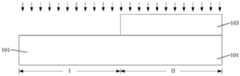
参考图1,提供衬底101,所述衬底101包括第一区域I和第二区域II。其中,图1为沿AA1(未图示)方向的剖面结构示意图,AA1方向与待形成的鳍部延伸方向相互垂直。Referring to FIG. 1, a
所述第一区域I为NMOS区域或PMOS区域,所述第二区域II为NMOS区域或PMOS区域。本实施例以形成的鳍式场效应管为CMOS器件为例,所述第一区域I为NMOS区域,所述第二区域II为PMOS区域。在其他实施例中,所述第一区域也能够为PMOS区域,相应的第二区域II为NMOS区域。The first region I is an NMOS region or a PMOS region, and the second region II is an NMOS region or a PMOS region. In this embodiment, the formed fin field effect transistor is taken as an example of a CMOS device, the first region I is an NMOS region, and the second region II is a PMOS region. In other embodiments, the first region can also be a PMOS region, and the corresponding second region II can be an NMOS region.
在其他实施例中,形成的鳍式场效应管为NMOS器件时,第一区域和第二区域均为NMOS区域;形成的鳍式场效应管为PMOS器件时,第一区域和第二区域均为PMOS区域。In other embodiments, when the formed fin field effect transistor is an NMOS device, the first region and the second region are both NMOS regions; when the formed fin field effect transistor is a PMOS device, both the first region and the second region are for the PMOS region.
所述衬底101的材料为硅、锗、锗化硅、碳化硅、砷化镓或镓化铟。所述衬底101还能够为绝缘体上的硅衬底或者绝缘体上的锗衬底。The material of the
本实施例中,所述衬底101的材料为硅。In this embodiment, the material of the
继续参考图1,在所述第二区域II衬底101内形成第二阱区(未图示)。Continuing to refer to FIG. 1 , a second well region (not shown) is formed in the second region II
具体的,在所述第一区域I衬底101表面形成第一光刻胶层102;以所述第一光刻胶层102为掩膜,对所述第二区域II衬底101进行离子注入,在所述PMOS区域II衬底101内形成第二阱区;去除所述第一光刻胶层102。Specifically, a
所述第二阱区内的掺杂离子为N型离子,例如为P离子、As离子或Sb离子。The doping ions in the second well region are N-type ions, such as P ions, As ions or Sb ions.
如无特别说明,后续工艺步骤提供的结构示意图均为在图1基础上的示意图。Unless otherwise specified, the structural schematic diagrams provided in the subsequent process steps are all schematic diagrams based on FIG. 1 .
参考图2,在所述第一区域I衬底101内形成第一阱区(未图示)。Referring to FIG. 2 , a first well region (not shown) is formed in the first
具体的,在所述第二区域II衬底101表面形成第二光刻胶层103;以所述第二光刻胶层103为掩膜,对所述第一区域I衬底101进行离子注入,在所述第一区域I衬底101内形成第一阱区;去除所述第二光刻胶层103。Specifically, a
所述第一阱区内的掺杂离子为P型离子,例如为B离子、Ga离子或In离子。The doping ions in the first well region are P-type ions, such as B ions, Ga ions or In ions.
在形成所述第一阱区和第二阱区之后,还包括步骤:对所述衬底101表面进行清洗处理,为后续形成金刚石膜提供良好的界面基础。After forming the first well region and the second well region, the method further includes the step of: cleaning the surface of the
参考图3,在所述衬底101表面形成金刚石膜104。Referring to FIG. 3 , a
所述金刚石膜104为后续形成鳍式场效应管的隔离结构提供工艺基础。The
所述金刚石膜104的材料为金刚石(Diamond Carbon)或类金刚石(Diamond likeCarbon)。由于金刚石膜104的材料热导率大于氧化硅的热导率,因此在所述金刚石膜104基础上形成的隔离结构具有较高的热传导率,有效的避免鳍式场效应管内出现自加热(self-heating)问题,使得鳍式场效应管具有良好的自加热免疫能力。The material of the
采用化学气相沉积工艺、物理气相沉积工艺或原子层沉积工艺形成所述金刚石膜104。在一个实施例中,形成所述金刚石膜104的工艺参数包括:将衬底加热至200℃~450℃之后,将所述衬底101置于碳氢化合物气体的等离子体中,在所述衬底施加500V~20kV的负脉冲偏压。本实施例中,所述碳氢化合物气体包括:甲烷、乙炔中的一种或多种;所述衬底101施加的负脉冲偏压为1kV~15kV;所述衬底101的温度大于300℃。The
参考图4,刻蚀所述金刚石膜104直至暴露出衬底101表面,在所述第一区域I金刚石膜104内形成第一通孔105,在所述第二区域II金刚石膜104内形成第二通孔106。Referring to FIG. 4 , the
在一实施例中,形成所述第一通孔105和第二通孔106的工艺步骤包括:在所述金刚石膜104表面形成图形化的光刻胶层;以所述图形化的光刻胶层为掩膜,刻蚀所述金刚石膜104直至暴露出衬底101表面,在所述第一区域I金刚石膜104内形成第一通孔105,在所述第二区域II金刚石膜104内形成第二通孔106;去除所述图形化的光刻胶层。In one embodiment, the process steps of forming the first through
本实施例中,所述第一通孔105的侧壁表面与衬底101表面相互垂直,第一通孔105顶部尺寸与底部尺寸相同;所述第二通孔106的侧壁表面与衬底101表面相互垂直,所述第二通孔106顶部尺寸与底部尺寸相同。在其他实施例中,所述第一通孔顶部尺寸还能够大于底部尺寸,或者第一通孔的顶部尺寸小于底部尺寸;所述第二通孔顶部尺寸还能够大于底部尺寸,或者第二通孔的顶部尺寸小于底部尺寸。In this embodiment, the sidewall surface of the first through
参考图5,在所述第一通孔105底部表面和第二通孔106底部表面形成第一绝缘层107。Referring to FIG. 5 , a first insulating
所述第一绝缘层107的材料晶格常数与衬底101的材料晶格常数具有较大的差别。The material lattice constant of the first insulating
本实施例中,所述第一绝缘层107的材料为氧化硅,采用热氧化工艺,氧化位于第一通孔105底部表面和第二通孔106底部表面的衬底101,形成所述第一绝缘层107。In this embodiment, the material of the first insulating
所述热氧化工艺对衬底101的氧化速率不宜过快,否则容易造成衬底101被氧化的厚度过厚。为此,本实施例中,采用热氧化工艺形成所述第一绝缘层107的工艺参数包括:O2流量为10sccm至200sccm,反应腔室温度为350摄氏度至650摄氏度。The oxidation rate of the
在其他实施例中,所述第一绝缘层的材料还能够为氮化硅。采用热氮化工艺,氮化位于第一通孔底部表面和第二通孔底部表面的衬底,形成所述第一绝缘层。在另一实施例中,所述第一绝缘层的材料还能够为氮氧化硅。In other embodiments, the material of the first insulating layer can also be silicon nitride. Using a thermal nitridation process, the substrate on the bottom surface of the first through hole and the bottom surface of the second through hole is nitrided to form the first insulating layer. In another embodiment, the material of the first insulating layer can also be silicon oxynitride.
在其他实施例中,还能够采用沉积工艺形成所述第一绝缘层,所述沉积工艺能够为化学气相沉积、物理气相沉积或原子层沉积,相应的,形成的第一绝缘层不仅位于第一通孔底部表面和第二通孔底部表面,还位于第一通孔侧壁表面、第二通孔侧壁表面以及金刚石膜顶部表面。In other embodiments, the first insulating layer can also be formed by a deposition process, and the deposition process can be chemical vapor deposition, physical vapor deposition or atomic layer deposition. Correspondingly, the formed first insulating layer is not only located in the first insulating layer The bottom surface of the through hole and the bottom surface of the second through hole are also located on the sidewall surface of the first through hole, the sidewall surface of the second through hole and the top surface of the diamond film.
参考图6,在所述第二通孔106(参考图5)底部表面的第一绝缘层107表面形成第一图形层108;以所述第一图形层108为掩膜,刻蚀去除第一通孔105底部表面的第一绝缘层107。Referring to FIG. 6 , a
所述第一图形层108为刻蚀去除位于第一通孔105底部表面的第一绝缘层107的掩膜。The
本实施例中,所述第一图形层108的材料为光刻胶,为了降低形成第一图形层108的工艺难度,所述第一图形层108还覆盖于第二区域II金刚石膜104表面。In this embodiment, the material of the
采用干法刻蚀工艺、湿法刻蚀工艺或干法刻蚀与湿法刻蚀相结合的工艺,刻蚀去除所述第一通孔105底部表面的第一绝缘层107。The first insulating
本实施例中,所述第一绝缘层107的材料为氧化硅,采用湿法刻蚀工艺刻蚀去除所述第一通孔105底部表面的第一绝缘层107,其中,湿法刻蚀工艺采用的刻蚀液体为氢氟酸溶液。采用所述湿法刻蚀工艺不仅能够刻蚀去除第一通孔105底部表面的第一绝缘层107,还能够对第一通孔105底部的衬底101表面进行清洗处理,为后续形成高质量的第一防穿通层提供界面基础。In this embodiment, the material of the first insulating
在刻蚀去除所述第一通孔105底部表面的第一绝缘层107之后,采用湿法去胶或灰化工艺去除所述第一图形层108。After the first insulating
参考图7,采用外延工艺,形成位于第一通孔105(参考图6)底部表面的第一外延层115、以及位于第一外延层115顶部表面的第一本征层125。Referring to FIG. 7 , an epitaxial process is used to form a
本实施例中,采用第一外延工艺形成所述第一外延层115;采用第二外延工艺形成所述第一本征层125。In this embodiment, the
所述第一外延层115内掺杂有第一防穿通离子,所述第一外延层115的材料包括硅、锗、锗化硅或碳化硅。所述第一防穿通离子与第一区域I待形成的源区和漏区的掺杂离子类型相反,本实施例中,所述第一区域I待形成的源区和漏区的掺杂离子为N型离子,则所述第一防穿通离子为P型离子,P型离子为硼离子、镓离子或铟离子。The
在采用第一外延工艺形成所述第一外延层115的过程中,原位自掺杂第一防穿通离子,所述第一防穿通离子包括硼离子。原位自掺杂所述第一防穿通离子,使得第一防穿通离子在第一外延层115内浓度分布均匀,且避免了离子注入工艺对第一外延层115带来的注入损伤。In the process of using the first epitaxial process to form the
所述第一外延层115能够与后续形成的第一本征层125内的源区或漏区构成PN结,在所述源区和漏区之间形成反向隔离,从而提高源区和漏区之间的穿通电压,以此防止源区和漏区之间发生穿通现象。The
由于第一通孔105底部表面材料为衬底101材料,第一通孔105侧壁表面材料为金刚石膜104材料,且第一外延层115的材料类型与衬底101的材料类型接近或相同,所述第一外延层115的材料晶格常数与衬底101的材料晶格常数接近,因此在采用第一外延工艺形成所述第一外延层115的过程中,沿着第一通孔105暴露出的衬底101表面晶向逐层生长薄膜,直至形成厚度符合预设目标的第一外延层115,因此所述第一外延层115为在衬底101表面自下而上生长的。Since the bottom surface material of the first through
同时,由于第二通孔106底部表面形成有第一绝缘层107,所述第一绝缘层107材料晶格常数与第一外延层115的材料晶格常数失配度较高,因此在第一外延工艺过程中,能够避免在第二通孔107内生长薄膜。At the same time, since the first insulating
本实施例中,所述第一外延层115的材料为掺杂有硼离子的硅,其中,硼离子浓度范围为1E19 atom/cm3~5E21 atom/cm3。采用第一外延工艺形成所述第一外延层115的工艺参数包括:腔室温度为500摄氏度至1250摄氏度,腔室压强为1托至100托,反应气体包括硅源气体、硼源气体、HCl和H2,硅源气体流量为1标况毫升/分钟至1000标况毫升/分钟,HCl流量为1标况毫升/分钟至1000标况毫升/分钟,H2流量为0.1标况升/分钟至50标况升/分钟。In this embodiment, the material of the
并且,所述第一防穿通离子类型与第一区域I衬底101内的第一阱区的掺杂类型相同,所述第一外延层115内的第一防穿通离子的掺杂浓度大于第一阱区的掺杂浓度,从而在NMOS器件内形成超陡逆行阱结构,所述超陡逆行阱能够提高形成于NMOS器件内的源区和漏区之间的穿通电压,以此防止NMOS器件内的源区和漏区之间发生穿通,且阻止衬底101内的掺杂离子向第一本征层125内扩散,防止NMOS器件的阈值电压漂移,使得器件的失配(Mismatch)好,因此半导体器件均匀性变好。In addition, the type of the first punch-through ions is the same as the doping type of the first well region in the first
所述第一本征层125作为第一区域I的鳍部,后续会在第一区域I的鳍部内形成源区、漏区以及沟道区。为了提高沟道区的载流子迁移率,所述第一本征层125的材料为III-V族元素化合物材料,其中,所述III-V族元素化合物材料为InGaAs、GaAs、InAs或InSb。所述第一本征层125的材料还能够为硅、锗、锗化硅或碳化硅。The first
本实施例中,采用第二外延工艺形成所述第一本征层125,所述第一本征层125的材料为InGaAs。In this embodiment, the first
所述第一本征层125的材料类型与衬底101的材料类型接近,相应的第一本征层125的材料类型与第一外延层115的材料类型接近,因此在采用第二外延工艺形成第一本征层125的过程中,沿着第一外延层115顶部表面的晶向逐层生长薄膜,直至形成厚度符合预设目标的第一本征层125,因此所述第一本征层125为在第一外延层115顶表面自下而上生长的。The material type of the first
同时,由于第二通孔106底部表面的第一绝缘层107材料晶格常数与第一本征层125的材料晶格常数相差较大,因此在第二外延工艺过程中也不会在第二通孔106内生长薄膜。At the same time, since the lattice constant of the material of the first insulating
所述第一本征层125的顶部至少高于金刚石膜104顶部,从而使得后续的研磨工艺能够对第一本征层125顶部进行研磨,从而获得顶部表面平坦的鳍部。The top of the first
本实施例中,形成第一外延层115的工艺未对第一本征层125造成不良影响,使得第一本征层125具有良好的性能,即第一区域I的鳍部具有良好的性能,从而进一步提高鳍式场效应管的电学性能。In this embodiment, the process of forming the
而现有技术中,为了防止源区和漏区之间发生穿通现象,通常采用离子注入工艺对鳍部底部进行掺杂处理,所述离子注入工艺会对鳍部造成注入损伤,造成鳍部内出现晶格缺陷,从而影响鳍式场效应管的电学性能。However, in the prior art, in order to prevent the punch-through phenomenon between the source region and the drain region, the bottom of the fin is usually doped by an ion implantation process. Lattice defects, thereby affecting the electrical performance of the fin field effect transistor.
参考图8,在所述第一本征层125顶部表面形成第二绝缘层109。Referring to FIG. 8 , a second insulating
所述第二绝缘层109的材料晶格常数与后续待形成的第二外延层以及第二本征层的材料晶格常数相差较大,从而使得后续的外延工艺过程不会在第一本征层125表面生长薄膜。The lattice constant of the material of the second insulating
为了避免所述第二绝缘层109对第一区域I的鳍部造成不良影响,所述第二绝缘层109底部高于金刚石膜104顶部。In order to prevent the second insulating
本实施例中,采用热氧化工艺形成所述第二绝缘层109,在所述第一本征层125顶部表面形成第二绝缘层109,所述第二绝缘层109的材料为掺氧的砷镓化铟。In this embodiment, the second insulating
在另一实施例中,所述第一本征层的材料为硅时,所述第二绝缘层109的材料为氧化硅。In another embodiment, when the material of the first intrinsic layer is silicon, the material of the second insulating
参考图9,去除位于第二通孔106底部表面的第一绝缘层107(参考图8)。Referring to FIG. 9, the first insulating
具体的,在所述第二绝缘层109表面以及第一区域I金刚石膜104表面形成第二图形层;以所述第二图形层为掩膜,刻蚀去除位于第二通孔106底部表面的第一绝缘层107;去除所述第二图形层。Specifically, a second pattern layer is formed on the surface of the second insulating
参考图10,采用外延工艺,形成位于第二通孔106(参考图9)底部表面的第二外延层116以及位于第二外延层116顶部表面的第二防穿通层126。Referring to FIG. 10 , an epitaxial process is used to form a
本实施例中,采用第三外延工艺形成所述第二外延层116;采用第四外延工艺形成所述第二本征层126。In this embodiment, the
所述第二外延层116内掺杂有第二防穿通离子,所述第二外延层116的材料包括硅、锗、锗化硅或碳化硅。所述第二防穿通离子与第二区域II待形成的源区和漏区的掺杂离子类型相反;本实施例中,所述第二区域II待形成的源区和漏区的掺杂离子为P型离子,则所述第二防穿通离子为N型离子,N型离子为磷离子、砷离子或锑离子。The
在采用第三外延工艺形成所述第二外延层116的过程中,原位自掺杂第二防穿通离子,所述第二防穿通离子包括磷离子。原位自掺杂所述第二防穿通离子,使得第二防穿通离子在所述第二外延层116内浓度分布均匀,且避免了离子注入工艺对第二外延层116带来的注入损伤。In the process of forming the
所述第二外延层116能够与后续形成的第二本征层126内的源区或漏区构成PN结,在所述源区和漏区之间形成反向隔离,从而提高源区和漏区之间的穿通电压,以此防止源区和漏区之间发生穿通现象。The
由于第二通孔106底部表面材料为衬底101材料,第二通孔106侧壁表面材料为金刚石膜104材料,且第二外延层116的材料类型与衬底101的材料类型接近或相同,所述第二外延层116的材料晶格常数与衬底101的材料晶格常数接近,因此在采用第三外延工艺形成所述第二外延层116的过程中,沿着第二通孔106暴露出的衬底101表面晶向逐层生长薄膜,直至形成厚度符合预设目标的第二外延层116,因此所述第二外延层116为在衬底101表面自下而上生长的。Since the material of the bottom surface of the second through
同时,由于第一本征层125顶部表面形成有第二绝缘层109,所述第二绝缘层109材料晶格常数与第二外延层116的材料晶格常数失配度高,因此在第三外延工艺过程中,能够避免在第一本征层125顶部表面生长薄膜。At the same time, since the second insulating
本实施例中,所述第二外延层116的材料为掺杂有磷离子的硅,其中,磷离子浓度范围为1E19 atom/cm3~6E21 atom/cm3。采用第三外延工艺形成所述第二外延层116的工艺参数包括:腔室温度为500摄氏度至1250摄氏度,腔室压强为1托至100托,反应气体包括硅源气体、磷源气体、HCl和H2,硅源气体流量为1标况毫升/分钟至1000标况毫升/分钟,HCl流量为1标况毫升/分钟至1000标况毫升/分钟,H2流量为0.1标况升/分钟至50标况升/分钟。In this embodiment, the material of the
并且,所述第二防穿通离子类型与第二区域II衬底101内的第二阱区的掺杂类型相同,所述第二外延层116内的第二防穿通离子的掺杂浓度大于第二阱区的掺杂浓度,从而在PMOS器件内形成超陡逆行阱结构,以此防止PMOS器件内的源区和漏区之间发生穿通,且阻止衬底101内的掺杂离子向第二本征层126内扩散,避免PMOS器件的阈值电压漂移。In addition, the second punch-through ion type is the same as the doping type of the second well region in the second region II
所述第二本征层126作为第二区域II的鳍部,后续会在第二区域II的鳍部内形成源区、漏区以及沟道区。为了提高沟道区的载流子迁移率,所述第二本征层126的材料为III-V族元素化合物材料,其中,所述III-V族元素化合物材料为InGaAs、GaAs、InAs或InSb。所述第二本征层126的材料还能够为硅、锗、锗化硅或碳化硅。The second
本实施例中,采用第四外延工艺形成所述第二本征层126,所述第二本征层126的材料为InGaAs。由于第一本征层125顶部表面形成有第二绝缘层109,所述第二绝缘层109材料晶格常数与第二本征层126材料晶格常数相差较大,因此在第四外延工艺过程中也不会在第二本征层126顶部表面生长薄膜。In this embodiment, the second
所述第二本征层126的顶部至少高于金刚石膜104顶部,从而使得后续的研磨工艺能对第二本征层126顶部进行研磨,从而获得顶部表面平坦的鳍部。The top of the second
本实施例中,形成第二外延层116的工艺未对第二本征层126造成不良影响,使得第二本征层126具有良好的性能,即第二区域II的鳍部具有良好的性能,从而进一步提高鳍式场效应管的电学性能。In this embodiment, the process of forming the
参考图11,对所述第一本征层125和第二本征层126进行平坦化处理,使得第一本征层125顶部、第二本征层126顶部与金刚石膜104顶部齐平。Referring to FIG. 11 , the first
具体的,对所述第一本征层125和第二本征层126顶部进行平坦化处理,去除高于金刚石膜104顶部表面的第一本征层125和第二本征层126,还去除位于第一本征层125顶部表面的第二绝缘层109(参考图10)。Specifically, a planarization process is performed on the tops of the first
本实施例中,采用化学机械研磨工艺进行所述平坦化处理,去除高于金刚石膜104顶部表面的第一本征层125、第二本征层126以及第二绝缘层109。In this embodiment, the chemical mechanical polishing process is used to perform the planarization treatment to remove the first
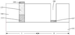
参考图12,回刻蚀去除部分厚度的金刚石膜104(参考图11)形成金刚石层114,所述金刚石层114暴露出第一本征层125侧壁表面和第二本征层126侧壁表面。Referring to FIG. 12 , a partial thickness of the diamond film 104 (refer to FIG. 11 ) is etched back to form a
本实施例中,所述第一本征层125底部高于所述金刚石层114顶部,所述第二本征层126底部高于所述金刚石层114顶部。在其他实施例中,所述第一本征层底部还能够与金刚石层顶部齐平,所述第二本征层底部还能够与金刚石层顶部齐平。In this embodiment, the bottom of the first
所述金刚石层114作为鳍式场效应管的隔离结构,起到电绝缘作用。且由于金刚石层114具有较高的热导率,使得鳍式场效应管内的热量能够及时的传递至外界,有效的改善了鳍式场效应管的自加热问题。The
采用干法刻蚀工艺、湿法刻蚀工艺或干法刻蚀工艺和湿法刻蚀工艺相结合的刻蚀工艺,回刻蚀去除部分厚度的金刚石膜104。在其他实施例中,还能够采用SiCoNi刻蚀系统进行所述回刻蚀。Using a dry etching process, a wet etching process, or an etching process combining the dry etching process and the wet etching process, the
参考图13,形成横跨所述第一本征层125的第一栅极结构131,所述第一栅极结构覆盖第一本征层125部分顶部表面和侧壁表面;形成横跨所述第二本征层126的第二栅极结构132,所述第二栅极结构132覆盖第二本征层126部分顶部表面和侧壁表面。Referring to FIG. 13, a
本实施例中,以所述第一栅极结构131为伪栅结构(dummy gate)、第二栅极结构132为伪栅结构为例。后续在第一区域I形成源区和漏区之后,去除所述第一栅极结构131,在所述第一栅极结构131所占据的位置处重新形成第一实际栅极结构;在第二区域II形成源区和漏区之后,去除所述第二栅极结构132,在所述第二栅极结构132所占据的位置处重新形成第二实际栅极结构。In this embodiment, the
所述第一栅极结构131的材料为多晶硅;所述第二栅极结构132的材料为多晶硅。The material of the
在其他实施例中,所述第一栅极结构和第二栅极结构还能够为实际栅极结构,所述第一栅极结构包括第一栅介质层和位于第一栅介质层顶部表面的第一栅电极层,所述第二栅极结构包括第二栅介质层和位于第二栅介质层顶部表面的第二栅电极层。In other embodiments, the first gate structure and the second gate structure can also be actual gate structures, and the first gate structure includes a first gate dielectric layer and a gate electrode located on the top surface of the first gate dielectric layer. A first gate electrode layer, the second gate structure includes a second gate dielectric layer and a second gate electrode layer on the top surface of the second gate dielectric layer.
结合参考图13至图14,图13为沿AA1方向的剖面结构示意图,图14为沿BB1(未图示)方向的剖面结构示意图,其中,AA1和BB1相互平行,在所述第一栅极结构131两侧的第一本征层125内形成第一源漏区133;在所述第二栅极结构132两侧的第二本征层126内形成第二源漏区134。13 to 14, FIG. 13 is a schematic cross-sectional structure diagram along the AA1 direction, and FIG. 14 is a cross-sectional structure schematic diagram along the BB1 (not shown) direction, wherein AA1 and BB1 are parallel to each other, and the first gate First source and drain
所述第一源漏区133用于形成NMOS器件的源极和漏极;所述第二源漏区134用于形成PMOS器件的源极和漏极。所述第一源漏区133内的掺杂离子类型与第一防穿通离子的掺杂类型相反,所述第一源漏区133内的掺杂离子为N型离子;所述第二源漏区134内的掺杂离子类型与第二防穿通离子的掺杂类型相反,所述第二源漏区134内的掺杂离子为P型离子。The first source and drain
本实施例中,所述第一源漏区133内的掺杂离子为P离子,P离子浓度为1E20atom/cm3至2E21atom/cm3。为了提高NMOS器件的载流子迁移率,所述第一源漏区133内形成有第一应力层(未标示)。所述第一应力层的材料为SiC或SiCP。In this embodiment, the doping ions in the first source and drain
形成所述第一源漏区133的工艺步骤包括:刻蚀所述第一栅极结构131两侧的部分厚度的第一本征层125,在所述第一本征层124内形成开口;形成填充满所述开口的第一应力层。The process steps of forming the first source and drain
采用选择性外延工艺形成所述第一应力层。本实施例中,在形成所述第一应力层的过程中进行原位自掺杂形成所述第一源漏区133。在其他实施例中,还能够在形成所述第一应力层之后,对所述第一应力层进行离子注入,形成所述第一源漏区。The first stressor layer is formed by a selective epitaxy process. In this embodiment, in-situ self-doping is performed to form the first source and drain
本实施例中,所述第二源漏区134内的掺杂离子为B离子。为了提高PMOS器件的载流子迁移率,所述第二源漏区134内还形成有第二应力层(未标示),所述第二应力层的材料为SiGe或SiGeB。形成所述第二源漏区134的工艺步骤包括:刻蚀所述第二栅极结构132两侧的部分厚度的第二本征层126,在所述第二本征层126内形成开口;形成填充满所述开口的第二应力层。In this embodiment, the dopant ions in the second source and drain
采用选择性外延工艺形成所述第二应力层。本实施例中,在形成所述第二应力层的过程中进行原位自掺杂形成所述第二源漏区134。在其他实施例中,还能够在形成所述第二应力层之后,对所述第二应力层进行离子注入,形成所述第二源漏区134。The second stressor layer is formed by a selective epitaxy process. In this embodiment, in-situ self-doping is performed to form the second source and drain
本实施例中,所述第一本征层125作为第一区域I的鳍部,所述第一区域I的鳍部未受到第一外延层115形成工艺的不良影响,使得第一区域I的第一本征层125具有良好的性能。且第二区域II的第二本征层126也未受到第二外延层116形成工艺的不良影响,使得第二区域II的第二本征层126也具有良好的性能。并且,本实施例中采用原位自掺杂的第一外延工艺形成所述第一外延层115,使得第一外延层115内的第一防穿通离子分布均匀,且避免了第一外延层115受到离子注入损伤,减少了第一外延层115内晶格缺陷,使得所述第一外延层115起到的反向隔离源区和漏区的作用更强,有效的避免第一区域I源区和漏区之间的穿通现象。In this embodiment, the first
同样的,本实施例中采用原位自掺杂的第三外延工艺形成所述第二外延层116,使得第二外延层116内的第二防穿通离子分布均匀,且避免了第二外延层116受到离子注入损伤,减少了第二外延层116内的晶格缺陷,使得所述第二外延层116起到的反向隔离源区和漏区的作用更强,有效的避免第二区域II源区和漏区之间的穿通现象。Similarly, in the present embodiment, the
如无特别说明,后续工艺步骤中提供的结构示意图均为在图13基础上的示意图。Unless otherwise specified, the structural schematic diagrams provided in the subsequent process steps are all schematic diagrams based on FIG. 13 .
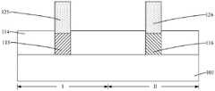
参考图15,在所述金刚石层114表面形成层间介质层200,所述层间介质层200覆盖于第一栅极结构131表面、第二栅极结构132表面、第一本征层125表面以及第二本征层126表面,所述层间介质层200顶部与第一栅极结构131顶部以及第二栅极结构132顶部齐平。Referring to FIG. 15 , an
所述层间介质层200的材料为氧化硅、氮化硅或氮氧化硅。本实施例中,所述层间介质层200的材料为氧化硅。The material of the
参考图16,去除所述第一栅极结构131(参考图15),在所述第一区域I层间介质层200内形成第一开口;形成填充满所述第一开口的第一实际栅极结构141。去除所述第二栅极结构132(参考图15),在所述第二区域II层间介质层200内形成第二开口;形成填充满所述第二开口的第二栅极结构142。Referring to FIG. 16 , the first gate structure 131 (refer to FIG. 15 ) is removed, and a first opening is formed in the
所述第一实际栅极结构141包括第一栅介质层和位于第一栅介质层表面的第二栅电极层,所述第一实际栅极结构141横跨所述第一本征层125,且覆盖第一本征层125部分顶部表面和侧壁表面。The first
所述第二实际栅极结构142包括第二栅介质层和位于第二栅介质层表面的第二栅电极层,所述第二实际栅极结构142横跨所述第二本征层126,且覆盖第二本征层126部分顶部表面和侧壁表面。The second
所述第一栅介质层的材料为氧化硅、氮化硅、氮氧化硅或高k栅介质材料;所述第二栅介质层的材料为氧化硅、氮化硅、氮氧化硅或高k栅介质材料。其中,所述高k栅介质材料指的是,相对介电常数大于氧化硅相对介电常数的材料,包括氧化铪、氧化锆、氧化铪硅、氧化镧、氧化锆硅、氧化钛、氧化钽、氧化钡锶钛、氧化钡钛、氧化锶钛或氧化铝。The material of the first gate dielectric layer is silicon oxide, silicon nitride, silicon oxynitride or high-k gate dielectric material; the material of the second gate dielectric layer is silicon oxide, silicon nitride, silicon oxynitride or high-k gate dielectric material. The high-k gate dielectric material refers to a material whose relative permittivity is greater than that of silicon oxide, including hafnium oxide, zirconium oxide, hafnium silicon oxide, lanthanum oxide, zirconium oxide silicon, titanium oxide, and tantalum oxide. , barium strontium titanium oxide, barium titanium oxide, strontium titanium oxide or aluminum oxide.
所述第一栅电极层的材料为多晶硅、掺杂的多晶硅、氮化钛、氮化钽、铜、钨、铝、金或银;所述第二栅电极层的材料为多晶硅、掺杂的多晶硅、氮化钛、氮化钽、铜、钨、铝、金或银。The material of the first gate electrode layer is polysilicon, doped polysilicon, titanium nitride, tantalum nitride, copper, tungsten, aluminum, gold or silver; the material of the second gate electrode layer is polysilicon, doped Polysilicon, Titanium Nitride, Tantalum Nitride, Copper, Tungsten, Aluminum, Gold or Silver.
虽然本发明披露如上,但本发明并非限定于此。任何本领域技术人员,在不脱离本发明的精神和范围内,均可作各种更动与修改,因此本发明的保护范围应当以权利要求所限定的范围为准。Although the present invention is disclosed above, the present invention is not limited thereto. Any person skilled in the art can make various changes and modifications without departing from the spirit and scope of the present invention. Therefore, the protection scope of the present invention should be based on the scope defined by the claims.
Claims (20)
Priority Applications (1)
| Application Number | Priority Date | Filing Date | Title |
|---|---|---|---|
| CN201510631671.2ACN106558493B (en) | 2015-09-29 | 2015-09-29 | Method for forming fin field effect transistor |
Applications Claiming Priority (1)
| Application Number | Priority Date | Filing Date | Title |
|---|---|---|---|
| CN201510631671.2ACN106558493B (en) | 2015-09-29 | 2015-09-29 | Method for forming fin field effect transistor |
Publications (2)
| Publication Number | Publication Date |
|---|---|
| CN106558493A CN106558493A (en) | 2017-04-05 |
| CN106558493Btrue CN106558493B (en) | 2020-10-09 |
Family
ID=58416953
Family Applications (1)
| Application Number | Title | Priority Date | Filing Date |
|---|---|---|---|
| CN201510631671.2AActiveCN106558493B (en) | 2015-09-29 | 2015-09-29 | Method for forming fin field effect transistor |
Country Status (1)
| Country | Link |
|---|---|
| CN (1) | CN106558493B (en) |
Families Citing this family (3)
| Publication number | Priority date | Publication date | Assignee | Title |
|---|---|---|---|---|
| CN106558498B (en)* | 2015-09-30 | 2019-11-01 | 中芯国际集成电路制造(上海)有限公司 | Semiconductor structure and forming method thereof |
| CN113363145B (en)* | 2020-03-05 | 2023-12-22 | 中芯国际集成电路制造(上海)有限公司 | Method for forming semiconductor structure |
| US11296080B2 (en)* | 2020-06-15 | 2022-04-05 | Taiwan Semiconductor Manufacturing Co., Ltd. | Source/drain regions of semiconductor devices and methods of forming the same |
Citations (4)
| Publication number | Priority date | Publication date | Assignee | Title |
|---|---|---|---|---|
| CN103531477A (en)* | 2012-07-05 | 2014-01-22 | 台湾积体电路制造股份有限公司 | FinFET method and structure with embedded underlying anti-punch through layer |
| CN103887177A (en)* | 2014-03-27 | 2014-06-25 | 上海集成电路研发中心有限公司 | Finned active area manufacturing method |
| US9099424B1 (en)* | 2012-08-10 | 2015-08-04 | Monolithic 3D Inc. | Semiconductor system, device and structure with heat removal |
| US20150255456A1 (en)* | 2014-03-04 | 2015-09-10 | Globalfoundries Inc. | Replacement fin insolation in a semiconductor device |
Family Cites Families (1)
| Publication number | Priority date | Publication date | Assignee | Title |
|---|---|---|---|---|
| CN103367227B (en)* | 2012-03-29 | 2015-09-23 | 中国科学院微电子研究所 | Semiconductor device manufacturing method |
- 2015
- 2015-09-29CNCN201510631671.2Apatent/CN106558493B/enactiveActive
Patent Citations (4)
| Publication number | Priority date | Publication date | Assignee | Title |
|---|---|---|---|---|
| CN103531477A (en)* | 2012-07-05 | 2014-01-22 | 台湾积体电路制造股份有限公司 | FinFET method and structure with embedded underlying anti-punch through layer |
| US9099424B1 (en)* | 2012-08-10 | 2015-08-04 | Monolithic 3D Inc. | Semiconductor system, device and structure with heat removal |
| US20150255456A1 (en)* | 2014-03-04 | 2015-09-10 | Globalfoundries Inc. | Replacement fin insolation in a semiconductor device |
| CN103887177A (en)* | 2014-03-27 | 2014-06-25 | 上海集成电路研发中心有限公司 | Finned active area manufacturing method |
Also Published As
| Publication number | Publication date |
|---|---|
| CN106558493A (en) | 2017-04-05 |
Similar Documents
| Publication | Publication Date | Title |
|---|---|---|
| US10541238B2 (en) | FinFET and fabrication method thereof | |
| CN107958873B (en) | Fin-type field effect transistor and method of forming the same | |
| CN103311247B (en) | Semiconductor device and method for manufacturing the same | |
| US8871584B2 (en) | Replacement source/drain finFET fabrication | |
| CN108122976B (en) | Semiconductor structure and method of forming the same, and SRAM | |
| CN107785261A (en) | Semiconductor structure and its manufacture method | |
| CN112151377B (en) | Semiconductor structure and forming method thereof | |
| CN104253046A (en) | Fin field effect transistor and forming method thereof | |
| CN117203768A (en) | Nanoflake mosfet with asymmetric threshold voltage | |
| CN103426769A (en) | Semiconductor device manufacturing method | |
| CN106952806A (en) | The Method of Improving the Performance of FinFET | |
| CN108630542A (en) | Semiconductor structure and forming method thereof | |
| CN106558493B (en) | Method for forming fin field effect transistor | |
| CN107591436B (en) | Fin type field effect transistor and forming method thereof | |
| CN103779223B (en) | MOSFET manufacturing method | |
| CN111463275A (en) | Semiconductor structure and method of forming the same | |
| CN111627814B (en) | Semiconductor structure and forming method thereof | |
| CN109087892B (en) | Semiconductor structure, forming method thereof and forming method of fin field effect transistor | |
| CN114068705B (en) | Semiconductor structure and forming method thereof | |
| CN111613672A (en) | Semiconductor structure and method of forming the same | |
| CN107437533B (en) | Semiconductor structure and method of making the same | |
| CN111276442B (en) | Semiconductor structure and forming method thereof | |
| CN111435645B (en) | Semiconductor structures and methods of forming them | |
| CN108630521B (en) | Method for manufacturing semiconductor device | |
| CN109427679B (en) | Semiconductor structure and method of forming the same |
Legal Events
| Date | Code | Title | Description |
|---|---|---|---|
| PB01 | Publication | ||
| PB01 | Publication | ||
| SE01 | Entry into force of request for substantive examination | ||
| SE01 | Entry into force of request for substantive examination | ||
| GR01 | Patent grant | ||
| GR01 | Patent grant |