CN106537898B - Image forming apparatus with a plurality of image forming units - Google Patents
Image forming apparatus with a plurality of image forming unitsDownload PDFInfo
- Publication number
- CN106537898B CN106537898BCN201580041308.3ACN201580041308ACN106537898BCN 106537898 BCN106537898 BCN 106537898BCN 201580041308 ACN201580041308 ACN 201580041308ACN 106537898 BCN106537898 BCN 106537898B
- Authority
- CN
- China
- Prior art keywords
- transistor
- oxide semiconductor
- layer
- film
- semiconductor layer
- Prior art date
- Legal status (The legal status is an assumption and is not a legal conclusion. Google has not performed a legal analysis and makes no representation as to the accuracy of the status listed.)
- Active
Links
Images


Classifications
- H—ELECTRICITY
- H10—SEMICONDUCTOR DEVICES; ELECTRIC SOLID-STATE DEVICES NOT OTHERWISE PROVIDED FOR
- H10F—INORGANIC SEMICONDUCTOR DEVICES SENSITIVE TO INFRARED RADIATION, LIGHT, ELECTROMAGNETIC RADIATION OF SHORTER WAVELENGTH OR CORPUSCULAR RADIATION
- H10F39/00—Integrated devices, or assemblies of multiple devices, comprising at least one element covered by group H10F30/00, e.g. radiation detectors comprising photodiode arrays
- H10F39/80—Constructional details of image sensors
- H10F39/806—Optical elements or arrangements associated with the image sensors
- G—PHYSICS
- G01—MEASURING; TESTING
- G01J—MEASUREMENT OF INTENSITY, VELOCITY, SPECTRAL CONTENT, POLARISATION, PHASE OR PULSE CHARACTERISTICS OF INFRARED, VISIBLE OR ULTRAVIOLET LIGHT; COLORIMETRY; RADIATION PYROMETRY
- G01J1/00—Photometry, e.g. photographic exposure meter
- G01J1/02—Details
- G01J1/04—Optical or mechanical part supplementary adjustable parts
- G01J1/0407—Optical elements not provided otherwise, e.g. manifolds, windows, holograms, gratings
- G01J1/0414—Optical elements not provided otherwise, e.g. manifolds, windows, holograms, gratings using plane or convex mirrors, parallel phase plates, or plane beam-splitters
- G—PHYSICS
- G01—MEASURING; TESTING
- G01J—MEASUREMENT OF INTENSITY, VELOCITY, SPECTRAL CONTENT, POLARISATION, PHASE OR PULSE CHARACTERISTICS OF INFRARED, VISIBLE OR ULTRAVIOLET LIGHT; COLORIMETRY; RADIATION PYROMETRY
- G01J1/00—Photometry, e.g. photographic exposure meter
- G01J1/02—Details
- G01J1/04—Optical or mechanical part supplementary adjustable parts
- G01J1/0488—Optical or mechanical part supplementary adjustable parts with spectral filtering
- G01J1/0492—Optical or mechanical part supplementary adjustable parts with spectral filtering using at least two different filters
- G—PHYSICS
- G01—MEASURING; TESTING
- G01J—MEASUREMENT OF INTENSITY, VELOCITY, SPECTRAL CONTENT, POLARISATION, PHASE OR PULSE CHARACTERISTICS OF INFRARED, VISIBLE OR ULTRAVIOLET LIGHT; COLORIMETRY; RADIATION PYROMETRY
- G01J1/00—Photometry, e.g. photographic exposure meter
- G01J1/42—Photometry, e.g. photographic exposure meter using electric radiation detectors
- G01J1/44—Electric circuits
- G01J1/46—Electric circuits using a capacitor
- G—PHYSICS
- G01—MEASURING; TESTING
- G01J—MEASUREMENT OF INTENSITY, VELOCITY, SPECTRAL CONTENT, POLARISATION, PHASE OR PULSE CHARACTERISTICS OF INFRARED, VISIBLE OR ULTRAVIOLET LIGHT; COLORIMETRY; RADIATION PYROMETRY
- G01J3/00—Spectrometry; Spectrophotometry; Monochromators; Measuring colours
- G01J3/28—Investigating the spectrum
- G01J3/2803—Investigating the spectrum using photoelectric array detector
- G—PHYSICS
- G01—MEASURING; TESTING
- G01J—MEASUREMENT OF INTENSITY, VELOCITY, SPECTRAL CONTENT, POLARISATION, PHASE OR PULSE CHARACTERISTICS OF INFRARED, VISIBLE OR ULTRAVIOLET LIGHT; COLORIMETRY; RADIATION PYROMETRY
- G01J3/00—Spectrometry; Spectrophotometry; Monochromators; Measuring colours
- G01J3/28—Investigating the spectrum
- G01J3/2823—Imaging spectrometer
- H—ELECTRICITY
- H04—ELECTRIC COMMUNICATION TECHNIQUE
- H04N—PICTORIAL COMMUNICATION, e.g. TELEVISION
- H04N23/00—Cameras or camera modules comprising electronic image sensors; Control thereof
- H04N23/10—Cameras or camera modules comprising electronic image sensors; Control thereof for generating image signals from different wavelengths
- H04N23/12—Cameras or camera modules comprising electronic image sensors; Control thereof for generating image signals from different wavelengths with one sensor only
- H—ELECTRICITY
- H04—ELECTRIC COMMUNICATION TECHNIQUE
- H04N—PICTORIAL COMMUNICATION, e.g. TELEVISION
- H04N25/00—Circuitry of solid-state image sensors [SSIS]; Control thereof
- H04N25/10—Circuitry of solid-state image sensors [SSIS]; Control thereof for transforming different wavelengths into image signals
- H04N25/11—Arrangement of colour filter arrays [CFA]; Filter mosaics
- H04N25/13—Arrangement of colour filter arrays [CFA]; Filter mosaics characterised by the spectral characteristics of the filter elements
- H04N25/134—Arrangement of colour filter arrays [CFA]; Filter mosaics characterised by the spectral characteristics of the filter elements based on three different wavelength filter elements
- H—ELECTRICITY
- H04—ELECTRIC COMMUNICATION TECHNIQUE
- H04N—PICTORIAL COMMUNICATION, e.g. TELEVISION
- H04N25/00—Circuitry of solid-state image sensors [SSIS]; Control thereof
- H04N25/70—SSIS architectures; Circuits associated therewith
- H04N25/76—Addressed sensors, e.g. MOS or CMOS sensors
- H—ELECTRICITY
- H04—ELECTRIC COMMUNICATION TECHNIQUE
- H04N—PICTORIAL COMMUNICATION, e.g. TELEVISION
- H04N25/00—Circuitry of solid-state image sensors [SSIS]; Control thereof
- H04N25/70—SSIS architectures; Circuits associated therewith
- H04N25/76—Addressed sensors, e.g. MOS or CMOS sensors
- H04N25/77—Pixel circuitry, e.g. memories, A/D converters, pixel amplifiers, shared circuits or shared components
- H04N25/778—Pixel circuitry, e.g. memories, A/D converters, pixel amplifiers, shared circuits or shared components comprising amplifiers shared between a plurality of pixels, i.e. at least one part of the amplifier must be on the sensor array itself
- H—ELECTRICITY
- H10—SEMICONDUCTOR DEVICES; ELECTRIC SOLID-STATE DEVICES NOT OTHERWISE PROVIDED FOR
- H10D—INORGANIC ELECTRIC SEMICONDUCTOR DEVICES
- H10D30/00—Field-effect transistors [FET]
- H10D30/60—Insulated-gate field-effect transistors [IGFET]
- H10D30/67—Thin-film transistors [TFT]
- H—ELECTRICITY
- H10—SEMICONDUCTOR DEVICES; ELECTRIC SOLID-STATE DEVICES NOT OTHERWISE PROVIDED FOR
- H10D—INORGANIC ELECTRIC SEMICONDUCTOR DEVICES
- H10D86/00—Integrated devices formed in or on insulating or conducting substrates, e.g. formed in silicon-on-insulator [SOI] substrates or on stainless steel or glass substrates
- H10D86/40—Integrated devices formed in or on insulating or conducting substrates, e.g. formed in silicon-on-insulator [SOI] substrates or on stainless steel or glass substrates characterised by multiple TFTs
- H10D86/421—Integrated devices formed in or on insulating or conducting substrates, e.g. formed in silicon-on-insulator [SOI] substrates or on stainless steel or glass substrates characterised by multiple TFTs having a particular composition, shape or crystalline structure of the active layer
- H10D86/423—Integrated devices formed in or on insulating or conducting substrates, e.g. formed in silicon-on-insulator [SOI] substrates or on stainless steel or glass substrates characterised by multiple TFTs having a particular composition, shape or crystalline structure of the active layer comprising semiconductor materials not belonging to the Group IV, e.g. InGaZnO
- H—ELECTRICITY
- H10—SEMICONDUCTOR DEVICES; ELECTRIC SOLID-STATE DEVICES NOT OTHERWISE PROVIDED FOR
- H10D—INORGANIC ELECTRIC SEMICONDUCTOR DEVICES
- H10D86/00—Integrated devices formed in or on insulating or conducting substrates, e.g. formed in silicon-on-insulator [SOI] substrates or on stainless steel or glass substrates
- H10D86/40—Integrated devices formed in or on insulating or conducting substrates, e.g. formed in silicon-on-insulator [SOI] substrates or on stainless steel or glass substrates characterised by multiple TFTs
- H10D86/481—Integrated devices formed in or on insulating or conducting substrates, e.g. formed in silicon-on-insulator [SOI] substrates or on stainless steel or glass substrates characterised by multiple TFTs integrated with passive devices, e.g. auxiliary capacitors
- H—ELECTRICITY
- H10—SEMICONDUCTOR DEVICES; ELECTRIC SOLID-STATE DEVICES NOT OTHERWISE PROVIDED FOR
- H10D—INORGANIC ELECTRIC SEMICONDUCTOR DEVICES
- H10D86/00—Integrated devices formed in or on insulating or conducting substrates, e.g. formed in silicon-on-insulator [SOI] substrates or on stainless steel or glass substrates
- H10D86/40—Integrated devices formed in or on insulating or conducting substrates, e.g. formed in silicon-on-insulator [SOI] substrates or on stainless steel or glass substrates characterised by multiple TFTs
- H10D86/60—Integrated devices formed in or on insulating or conducting substrates, e.g. formed in silicon-on-insulator [SOI] substrates or on stainless steel or glass substrates characterised by multiple TFTs wherein the TFTs are in active matrices
- H—ELECTRICITY
- H10—SEMICONDUCTOR DEVICES; ELECTRIC SOLID-STATE DEVICES NOT OTHERWISE PROVIDED FOR
- H10F—INORGANIC SEMICONDUCTOR DEVICES SENSITIVE TO INFRARED RADIATION, LIGHT, ELECTROMAGNETIC RADIATION OF SHORTER WAVELENGTH OR CORPUSCULAR RADIATION
- H10F39/00—Integrated devices, or assemblies of multiple devices, comprising at least one element covered by group H10F30/00, e.g. radiation detectors comprising photodiode arrays
- H10F39/011—Manufacture or treatment of image sensors covered by group H10F39/12
- H10F39/014—Manufacture or treatment of image sensors covered by group H10F39/12 of CMOS image sensors
- H—ELECTRICITY
- H10—SEMICONDUCTOR DEVICES; ELECTRIC SOLID-STATE DEVICES NOT OTHERWISE PROVIDED FOR
- H10F—INORGANIC SEMICONDUCTOR DEVICES SENSITIVE TO INFRARED RADIATION, LIGHT, ELECTROMAGNETIC RADIATION OF SHORTER WAVELENGTH OR CORPUSCULAR RADIATION
- H10F39/00—Integrated devices, or assemblies of multiple devices, comprising at least one element covered by group H10F30/00, e.g. radiation detectors comprising photodiode arrays
- H10F39/10—Integrated devices
- H10F39/12—Image sensors
- H10F39/18—Complementary metal-oxide-semiconductor [CMOS] image sensors; Photodiode array image sensors
- H10F39/182—Colour image sensors
- H—ELECTRICITY
- H10—SEMICONDUCTOR DEVICES; ELECTRIC SOLID-STATE DEVICES NOT OTHERWISE PROVIDED FOR
- H10F—INORGANIC SEMICONDUCTOR DEVICES SENSITIVE TO INFRARED RADIATION, LIGHT, ELECTROMAGNETIC RADIATION OF SHORTER WAVELENGTH OR CORPUSCULAR RADIATION
- H10F39/00—Integrated devices, or assemblies of multiple devices, comprising at least one element covered by group H10F30/00, e.g. radiation detectors comprising photodiode arrays
- H10F39/80—Constructional details of image sensors
- H10F39/802—Geometry or disposition of elements in pixels, e.g. address-lines or gate electrodes
- H—ELECTRICITY
- H10—SEMICONDUCTOR DEVICES; ELECTRIC SOLID-STATE DEVICES NOT OTHERWISE PROVIDED FOR
- H10F—INORGANIC SEMICONDUCTOR DEVICES SENSITIVE TO INFRARED RADIATION, LIGHT, ELECTROMAGNETIC RADIATION OF SHORTER WAVELENGTH OR CORPUSCULAR RADIATION
- H10F39/00—Integrated devices, or assemblies of multiple devices, comprising at least one element covered by group H10F30/00, e.g. radiation detectors comprising photodiode arrays
- H10F39/80—Constructional details of image sensors
- H10F39/803—Pixels having integrated switching, control, storage or amplification elements
- H10F39/8037—Pixels having integrated switching, control, storage or amplification elements the integrated elements comprising a transistor
- H10F39/80377—Pixels having integrated switching, control, storage or amplification elements the integrated elements comprising a transistor characterised by the channel of the transistor, e.g. channel having a doping gradient
- H—ELECTRICITY
- H10—SEMICONDUCTOR DEVICES; ELECTRIC SOLID-STATE DEVICES NOT OTHERWISE PROVIDED FOR
- H10F—INORGANIC SEMICONDUCTOR DEVICES SENSITIVE TO INFRARED RADIATION, LIGHT, ELECTROMAGNETIC RADIATION OF SHORTER WAVELENGTH OR CORPUSCULAR RADIATION
- H10F39/00—Integrated devices, or assemblies of multiple devices, comprising at least one element covered by group H10F30/00, e.g. radiation detectors comprising photodiode arrays
- H10F39/80—Constructional details of image sensors
- H10F39/806—Optical elements or arrangements associated with the image sensors
- H10F39/8063—Microlenses
- H—ELECTRICITY
- H10—SEMICONDUCTOR DEVICES; ELECTRIC SOLID-STATE DEVICES NOT OTHERWISE PROVIDED FOR
- H10F—INORGANIC SEMICONDUCTOR DEVICES SENSITIVE TO INFRARED RADIATION, LIGHT, ELECTROMAGNETIC RADIATION OF SHORTER WAVELENGTH OR CORPUSCULAR RADIATION
- H10F99/00—Subject matter not provided for in other groups of this subclass
- G—PHYSICS
- G01—MEASURING; TESTING
- G01J—MEASUREMENT OF INTENSITY, VELOCITY, SPECTRAL CONTENT, POLARISATION, PHASE OR PULSE CHARACTERISTICS OF INFRARED, VISIBLE OR ULTRAVIOLET LIGHT; COLORIMETRY; RADIATION PYROMETRY
- G01J1/00—Photometry, e.g. photographic exposure meter
- G01J1/42—Photometry, e.g. photographic exposure meter using electric radiation detectors
- G01J1/44—Electric circuits
- G01J2001/4446—Type of detector
- G01J2001/446—Photodiode
- G—PHYSICS
- G01—MEASURING; TESTING
- G01J—MEASUREMENT OF INTENSITY, VELOCITY, SPECTRAL CONTENT, POLARISATION, PHASE OR PULSE CHARACTERISTICS OF INFRARED, VISIBLE OR ULTRAVIOLET LIGHT; COLORIMETRY; RADIATION PYROMETRY
- G01J3/00—Spectrometry; Spectrophotometry; Monochromators; Measuring colours
- G01J3/28—Investigating the spectrum
- G01J3/2803—Investigating the spectrum using photoelectric array detector
- G01J2003/2813—2D-array
- H—ELECTRICITY
- H04—ELECTRIC COMMUNICATION TECHNIQUE
- H04N—PICTORIAL COMMUNICATION, e.g. TELEVISION
- H04N23/00—Cameras or camera modules comprising electronic image sensors; Control thereof
- H04N23/50—Constructional details
- H04N23/53—Constructional details of electronic viewfinders, e.g. rotatable or detachable
- H04N23/531—Constructional details of electronic viewfinders, e.g. rotatable or detachable being rotatable or detachable
- H—ELECTRICITY
- H04—ELECTRIC COMMUNICATION TECHNIQUE
- H04N—PICTORIAL COMMUNICATION, e.g. TELEVISION
- H04N25/00—Circuitry of solid-state image sensors [SSIS]; Control thereof
- H04N25/50—Control of the SSIS exposure
- H04N25/53—Control of the integration time
- H04N25/532—Control of the integration time by controlling global shutters in CMOS SSIS
- H—ELECTRICITY
- H10—SEMICONDUCTOR DEVICES; ELECTRIC SOLID-STATE DEVICES NOT OTHERWISE PROVIDED FOR
- H10D—INORGANIC ELECTRIC SEMICONDUCTOR DEVICES
- H10D30/00—Field-effect transistors [FET]
- H10D30/60—Insulated-gate field-effect transistors [IGFET]
- H10D30/67—Thin-film transistors [TFT]
- H10D30/674—Thin-film transistors [TFT] characterised by the active materials
- H10D30/6755—Oxide semiconductors, e.g. zinc oxide, copper aluminium oxide or cadmium stannate
Landscapes
- Physics & Mathematics (AREA)
- Spectroscopy & Molecular Physics (AREA)
- Engineering & Computer Science (AREA)
- General Physics & Mathematics (AREA)
- Multimedia (AREA)
- Signal Processing (AREA)
- Power Engineering (AREA)
- Solid State Image Pick-Up Elements (AREA)
- Transforming Light Signals Into Electric Signals (AREA)
- Color Television Image Signal Generators (AREA)
- Electromagnetism (AREA)
Abstract
Description
Translated fromChinese技术领域technical field
本发明的一个方式涉及成像装置。One aspect of the present invention relates to an imaging device.
注意,本发明的一个方式不局限于上述技术领域。本说明书等所 公开的发明的一个方式的技术领域涉及一种物体、方法或者制造方法。 此外,本发明的一个方式涉及一种工序(process)、机器(machine)、 产品(manufacture)或者组合物(compositionofmatter)。由此,具体 而言,作为本说明书所公开的本发明的一个方式的技术领域的例子可 以举出半导体装置、显示装置、液晶显示装置、发光装置、照明装置、 蓄电装置、存储装置、成像装置、这些装置的驱动方法或者这些装置 的制造方法。Note that one form of the present invention is not limited to the above-mentioned technical field. The technical field of one aspect of the invention disclosed in this specification and the like relates to an object, a method, or a manufacturing method. Moreover, one form of this invention relates to a process (process), machine (machine), product (manufacture) or composition (composition of matter). Thus, specifically, examples of the technical field of one embodiment of the present invention disclosed in this specification include semiconductor devices, display devices, liquid crystal display devices, light-emitting devices, lighting devices, power storage devices, storage devices, imaging devices A device, a method of driving the device, or a method of manufacturing the device.
在本说明书等中,半导体装置是指通过利用半导体特性而能够工 作的所有装置。晶体管、半导体电路为半导体装置的一个方式。另外, 存储装置、显示装置、成像装置、电子设备有时包含半导体装置。In this specification and the like, a semiconductor device refers to any device that can operate by utilizing semiconductor characteristics. A transistor and a semiconductor circuit are one form of a semiconductor device. In addition, a storage device, a display device, an imaging device, and an electronic device sometimes include a semiconductor device.
背景技术Background technique
作为其中具有光电传感器的像素配置为矩阵状的半导体装置,已 知CMOS(Complementary Metal Oxide Semiconductor:互补金属氧化 物半导体)图像传感器。作为成像元件CMOS图像传感器被设置在如 数码相机或手机等众多便携式设备中。近年来,成像的清晰度增加、 便携式设备被小型化、且功耗被减少,因此CMOS图像传感器中的像 素被制造得更小。As a semiconductor device in which pixels having photosensors are arranged in a matrix, a CMOS (Complementary Metal Oxide Semiconductor) image sensor is known. As an imaging element, CMOS image sensors are provided in many portable devices such as digital cameras or cellular phones. In recent years, the sharpness of imaging has increased, portable devices have been miniaturized, and power consumption has been reduced, so that pixels in CMOS image sensors have been made smaller.
在CMOS图像传感器中,在光电传感器上形成滤色片,使用该滤 色片对入射光进行分光,然后使用光电传感器检测出各颜色的光,由 此取得彩色的成像数据。然而,因为滤色片透射特定波长范围的光并 吸收其他波长的光,所以入射光的利用效率低。因此,专利文献1公 开了使用对入射光进行分光的构成要素代替滤色片的技术。In a CMOS image sensor, a color filter is formed on a photoelectric sensor, incident light is separated by using the color filter, and light of each color is detected by the photoelectric sensor, thereby obtaining color imaging data. However, since the color filter transmits light of a specific wavelength range and absorbs light of other wavelengths, the utilization efficiency of incident light is low. Therefore,
[专利文献1]国际公开第2009/153937号小册子[Patent Document 1] International Publication No. 2009/153937 Pamphlet
在专利文献1的结构中,为了取得RGB各颜色的成像数据而需要 对直接取得的数据进行使用外部的处理电路的运算处理。由此,为了 实现成像装置的低功耗化或高速化而优选采用能够省略上述运算处理 等的结构。In the configuration of
发明内容SUMMARY OF THE INVENTION
因此,本发明的一个方式的目的之一是提供一种为了取得各颜色 的成像数据而不需要进行使用外部的处理电路的运算处理的成像装 置。本发明的一个方式的其他目的之一是提供一种能够拍摄彩色图像 而不使用滤色片的成像装置。本发明的一个方式的其他目的之一是提 供一种耗电量低的成像装置。本发明的一个方式的其他目的之一是提 供一种适于高速工作的成像装置。本发明的一个方式的其他目的之一 是提供一种高灵敏度的成像装置。本发明的一个方式的其他目的之一 是提供一种动态范围较广的成像装置。本发明的一个方式的其他目的 之一是提供一种高分辨率的成像装置。本发明的一个方式的其他目的 之一是提供一种低成本的成像装置。本发明的一个方式的其他目的之 一是提供一种高可靠性的成像装置。本发明的一个方式的其他目的之 一是提供一种新颖的成像装置等。本发明的一个方式的其他目的之一 是提供一种新颖的半导体装置等。Therefore, an object of one embodiment of the present invention is to provide an imaging apparatus that does not require arithmetic processing using an external processing circuit in order to acquire imaging data of each color. One of the other objects of one aspect of the present invention is to provide an imaging apparatus capable of capturing a color image without using a color filter. One of the other objects of one aspect of the present invention is to provide an image forming apparatus with low power consumption. One of the other objects of one aspect of the present invention is to provide an image forming apparatus suitable for high-speed operation. One of the other objects of one embodiment of the present invention is to provide a high-sensitivity imaging device. One of the other objects of one aspect of the present invention is to provide an imaging device with a wide dynamic range. One of the other objects of one aspect of the present invention is to provide a high-resolution imaging device. One of the other objects of one aspect of the present invention is to provide a low-cost image forming apparatus. Another object of one embodiment of the present invention is to provide a highly reliable image forming apparatus. Another object of one embodiment of the present invention is to provide a novel imaging device and the like. Another object of one embodiment of the present invention is to provide a novel semiconductor device or the like.
注意,这些目的的记载不妨碍其他目的的存在。此外,本发明的 一个方式并不需要实现所有上述目的。除上述目的外的目的从说明书、 附图、权利要求书等的记载中是显而易见的,并且可以从说明书、附 图、权利要求书等的所述记载中抽出。Note that the description of these purposes does not prevent the existence of other purposes. Furthermore, one form of the present invention need not achieve all of the above objects. Objects other than the above-mentioned objects are obvious from the description of the specification, drawings, claims, and the like, and can be extracted from the description of the specification, drawings, claims, and the like.
本发明的一个方式涉及一种包括分光元件的成像装置。One aspect of the present invention relates to an imaging device including a spectroscopic element.
本发明的一个方式是一种成像装置,包括:像素电路;以及分光 元件,其中,像素电路包括第一电路、第二电路、第三电路及第一电 容元件,第一电路包括第一光电转换元件、第一晶体管及第二晶体管, 第二电路包括第二光电转换元件、第三晶体管及第四晶体管,第三电 路包括第五晶体管、第六晶体管、第七晶体管及第二电容元件,分光 元件设置在第一光电转换元件或第二光电转换元件上,第一光电转换 元件的一个端子与第一晶体管的源极和漏极中的一个电连接,第二晶 体管的源极和漏极中的一个与第一晶体管的源极和漏极中的一个电连 接,第一晶体管的源极和漏极中的另一个与第一电容元件的一个端子 电连接,第二光电转换元件的一个端子与第三晶体管的源极和漏极中 的一个电连接,第四晶体管的源极和漏极中的一个与第三晶体管的源 极和漏极中的一个电连接,第四晶体管的源极和漏极中的另一个与第 一电容元件的一个端子电连接,第五晶体管的源极和漏极中的一个与 第一电容元件的另一个端子电连接,第二电容元件的一个端子与第一电容元件的另一个端子电连接,第六晶体管的栅极与第一电容元件的 另一个端子电连接,并且,第六晶体管的源极和漏极中的一个与第七 晶体管的源极和漏极中的一个电连接。One aspect of the present invention is an imaging device including: a pixel circuit; and a light splitting element, wherein the pixel circuit includes a first circuit, a second circuit, a third circuit, and a first capacitive element, and the first circuit includes a first photoelectric conversion element element, a first transistor and a second transistor, the second circuit includes a second photoelectric conversion element, a third transistor and a fourth transistor, the third circuit includes a fifth transistor, a sixth transistor, a seventh transistor and a second capacitive element, the light split The element is arranged on the first photoelectric conversion element or the second photoelectric conversion element, one terminal of the first photoelectric conversion element is electrically connected to one of the source electrode and the drain electrode of the first transistor, and the source electrode and the drain electrode of the second transistor are One is electrically connected to one of the source and drain of the first transistor, the other of the source and drain of the first transistor is electrically connected to one terminal of the first capacitive element, and one terminal of the second photoelectric conversion element electrically connected to one of the source and drain of the third transistor, one of the source and drain of the fourth transistor is electrically connected to one of the source and drain of the third transistor, the source of the fourth transistor The other one of the drain and the drain is electrically connected to one terminal of the first capacitive element, one of the source and drain of the fifth transistor is electrically connected to the other terminal of the first capacitive element, and one terminal of the second capacitive element is electrically connected to The other terminal of the first capacitive element is electrically connected, the gate of the sixth transistor is electrically connected to the other terminal of the first capacitive element, and one of the source and the drain of the sixth transistor is electrically connected to the source of the seventh transistor is electrically connected to one of the drains.
第一光电转换元件及第二光电转换元件优选具有相同的结构。The first photoelectric conversion element and the second photoelectric conversion element preferably have the same structure.
第一电容元件的电容值优选大于第二电容元件的电容值。The capacitance value of the first capacitive element is preferably larger than the capacitance value of the second capacitive element.
第一光电转换元件的一个端子、第一晶体管的源极和漏极中的一 个以及第一电容元件的一个端子之间的电容值优选等于第二光电转换 元件的一个端子、第三晶体管的源极和漏极中的一个以及第一电容元 件的一个端子之间的电容值。The capacitance value between one terminal of the first photoelectric conversion element, one of the source and drain of the first transistor, and one terminal of the first capacitive element is preferably equal to the one terminal of the second photoelectric conversion element, the source of the third transistor A capacitance value between one of the electrode and the drain and one terminal of the first capacitive element.
分光元件可以设置在第一光电转换元件上,从入射到像素电路的 光(W)去除了与红色(R)、绿色(G)、蓝色(B)对应的波长的光 成分中的任何一个的W-R、W-G或W-B的光可以入射到第一光电转 换元件,合成了入射到像素电路的光(W)及去除的光的W+R、W+G 或W+B可以入射到第二光电转换元件。A spectroscopic element may be provided on the first photoelectric conversion element to remove any one of light components of wavelengths corresponding to red (R), green (G), and blue (B) from light (W) incident on the pixel circuit The W-R, W-G, or W-B light can be incident on the first photoelectric conversion element, and W+R, W+G or W+B, which combines the light (W) incident on the pixel circuit and the removed light, can be incident on the second photoelectric conversion element. conversion element.
在上述结构中,相邻的像素中的上述去除的光的一部分也可以入 射到第二光电转换元件。In the above-mentioned structure, a part of the above-mentioned removed light in the adjacent pixels may also be incident on the second photoelectric conversion element.
另外,分光元件也可以设置在第二光电转换元件上,从入射到像 素电路的光(W)去除了与红色(R)、绿色(G)、蓝色(B)对应的 波长的光成分的1/2中的任何两个的W-(R/2)-(B/2)、W-(R/2)- (G/2)或W-(B/2)-(G/2)的光也可以入射到第二光电转换元件, 合成了入射到像素电路的光(W)及去除的光的W+(R/2)+(B/2)、 W+(R/2)+(G/2)或W+(B/2)+(G/2)也可以入射到第一光电转 换元件。Alternatively, a spectroscopic element may be provided on the second photoelectric conversion element to remove light components of wavelengths corresponding to red (R), green (G), and blue (B) from light (W) incident on the pixel circuit. W-(R/2)-(B/2), W-(R/2)-(G/2) or W-(B/2)-(G/2) of any two of 1/2 The light emitted from the pixel circuit can also be incident on the second photoelectric conversion element, and W+(R/2)+(B/2), W+(R/2)+(G and W+(R/2)+(B/2), W+(R/2)+(G /2) or W+(B/2)+(G/2) may also be incident on the first photoelectric conversion element.
第一至第七晶体管的一部分或全部优选在活性层中包含氧化物半 导体,该氧化物半导体优选包含In、Zn及M(M为Al、Ti、Ga、Sn、 Y、Zr、La、Ce、Nd或Hf)。Part or all of the first to seventh transistors preferably contain an oxide semiconductor in the active layer, and the oxide semiconductor preferably contains In, Zn, and M (M is Al, Ti, Ga, Sn, Y, Zr, La, Ce, Nd or Hf).
根据本发明的一个方式可以提供一种能够得到高质量的成像数据 的成像装置。另外,本发明的一个方式可以提供一种能够补偿像素电 路所包括的放大晶体管的电特性的成像装置。另外,本发明的一个方 式可以提供一种耗电量低的成像装置。另外,本发明的一个方式可以 提供一种适于高速工作的成像装置。另外,本发明的一个方式可以提 供一种高灵敏度的成像装置。另外,本发明的一个方式可以提供一种 动态范围较广的成像装置。另外,本发明的一个方式可以提供一种高 分辨率的成像装置。另外,本发明的一个方式可以提供一种低成本的 成像装置。另外,本发明的一个方式可以提供一种高可靠性的成像装 置。另外,本发明的一个方式可以提供一种新颖的成像装置等。另外, 本发明的一个方式可以提供一种新颖的半导体装置等。According to one aspect of the present invention, an imaging apparatus capable of obtaining high-quality imaging data can be provided. In addition, one embodiment of the present invention can provide an imaging device capable of compensating for electrical characteristics of an amplifier transistor included in a pixel circuit. In addition, one aspect of the present invention can provide an image forming apparatus with low power consumption. In addition, one aspect of the present invention can provide an image forming apparatus suitable for high-speed operation. In addition, one aspect of the present invention can provide a high-sensitivity imaging device. In addition, one aspect of the present invention can provide an imaging device with a wide dynamic range. In addition, one embodiment of the present invention can provide a high-resolution imaging device. In addition, one aspect of the present invention can provide a low-cost imaging device. In addition, one embodiment of the present invention can provide a highly reliable image forming apparatus. In addition, one aspect of the present invention can provide a novel imaging device and the like. In addition, one embodiment of the present invention can provide a novel semiconductor device and the like.
注意,这些效果的记载不妨碍其他效果的存在。注意,本发明的 一个方式并不需要具有所有上述效果。另外,可以从说明书、附图、 权利要求书等的记载显而易见地看出并抽出这些效果外的效果。Note that the description of these effects does not prevent the existence of other effects. Note that one form of the present invention does not need to have all of the above effects. In addition, effects other than these effects can be clearly seen and extracted from the description of the specification, drawings, claims, and the like.
附图说明Description of drawings
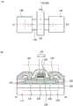
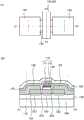
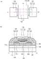
图1是成像装置所包括的像素的电路图;1 is a circuit diagram of a pixel included in an imaging device;
图2是说明成像装置所包括的分光元件及光电转换元件的位置关 系的示意图;2 is a schematic diagram illustrating the positional relationship of a spectroscopic element and a photoelectric conversion element included in the imaging device;
图3是说明成像装置所包括的分光元件及光电转换元件的位置关 系的示意图;3 is a schematic diagram illustrating the positional relationship of a spectroscopic element and a photoelectric conversion element included in the imaging device;
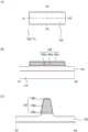
图4是说明像素的方式的俯视图;FIG. 4 is a plan view illustrating the manner of a pixel;
图5是说明像素的截面的图;5 is a diagram illustrating a cross-section of a pixel;
图6是说明像素电路的工作的时序图;6 is a timing chart illustrating the operation of the pixel circuit;
图7是像素电路及说明像素电路的工作的时序图;7 is a pixel circuit and a timing diagram illustrating the operation of the pixel circuit;
图8是成像装置所包括的像素的电路图;8 is a circuit diagram of a pixel included in the imaging device;
图9是说明像素的排列的图;9 is a diagram illustrating the arrangement of pixels;
图10是包括电路部的成像装置的截面图;10 is a cross-sectional view of an imaging device including a circuit portion;
图11是说明弯曲的成像装置的图;11 is a diagram illustrating a curved imaging device;
图12是说明全局快门方式的工作的时序图;12 is a timing chart illustrating the operation of the global shutter mode;
图13是说明卷帘快门方式的工作的时序图;13 is a timing chart illustrating the operation of the rolling shutter mode;
图14是说明晶体管的俯视图及截面图;14 is a plan view and a cross-sectional view illustrating a transistor;
图15是说明晶体管的俯视图及截面图;15 is a plan view and a cross-sectional view illustrating a transistor;
图16是说明晶体管的俯视图及截面图;16 is a plan view and a cross-sectional view illustrating a transistor;
图17是说明晶体管的俯视图及截面图;17 is a plan view and a cross-sectional view illustrating a transistor;
图18是说明晶体管的俯视图及截面图;18 is a plan view and a cross-sectional view illustrating a transistor;
图19是说明晶体管的俯视图及截面图;19 is a plan view and a cross-sectional view illustrating a transistor;
图20是说明晶体管的沟道宽度方向上的截面的图;20 is a diagram illustrating a cross section in the channel width direction of a transistor;
图21是说明晶体管的沟道长度方向上的截面的图;21 is a diagram illustrating a cross section in the channel length direction of a transistor;
图22是说明半导体层的俯视图及截面图;22 is a plan view and a cross-sectional view illustrating a semiconductor layer;
图23是说明半导体层的俯视图及截面图;23 is a plan view and a cross-sectional view illustrating a semiconductor layer;
图24是说明晶体管的俯视图及截面图;24 is a plan view and a cross-sectional view illustrating a transistor;
图25是说明晶体管的俯视图及截面图;25 is a plan view and a cross-sectional view illustrating a transistor;
图26是说明晶体管的俯视图及截面图;26 is a plan view and a cross-sectional view illustrating a transistor;
图27是说明晶体管的俯视图及截面图;27 is a plan view and a cross-sectional view illustrating a transistor;
图28是说明晶体管的俯视图及截面图;28 is a plan view and a cross-sectional view illustrating a transistor;
图29是说明晶体管的俯视图及截面图;29 is a plan view and a cross-sectional view illustrating a transistor;
图30是说明晶体管的沟道宽度方向上的截面的图;30 is a diagram illustrating a cross section in the channel width direction of a transistor;
图31是说明晶体管的沟道长度方向上的截面的图;31 is a diagram illustrating a cross section in the channel length direction of a transistor;
图32是说明晶体管的俯视图;32 is a top view illustrating a transistor;
图33是说明晶体管的制造方法的图;33 is a diagram illustrating a method of manufacturing a transistor;
图34是说明晶体管的制造方法的图;34 is a diagram illustrating a method of manufacturing a transistor;
图35是说明晶体管的制造方法的图;35 is a diagram illustrating a method of manufacturing a transistor;
图36是说明晶体管的制造方法的图;36 is a diagram illustrating a method of manufacturing a transistor;
图37是说明晶体管的制造方法的图;37 is a diagram illustrating a method of manufacturing a transistor;
图38是说明晶体管的制造方法的图;38 is a diagram illustrating a method of manufacturing a transistor;
图39是说明电子设备的图;39 is a diagram illustrating an electronic device;
图40是成像装置所包括的像素的电路图;40 is a circuit diagram of a pixel included in an imaging device;
图41是成像装置所包括的像素的电路图;41 is a circuit diagram of a pixel included in an imaging device;
图42是说明像素的方式的俯视图。FIG. 42 is a plan view illustrating a mode of a pixel.
具体实施方式Detailed ways
参照附图对实施方式进行详细说明。注意,本发明不局限于以下 说明,所属技术领域的普通技术人员可以很容易地理解一个事实就是, 本发明的方式及详细内容在不脱离本发明的宗旨及其范围的情况下可 以被变换为各种各样的形式。因此,本发明不应该被解释为仅限定于 以下所示的实施方式的记载内容中。注意,在以下说明的发明的结构 中,在不同的附图中共同使用相同的附图标记来表示相同的部分或具 有相同功能的部分,而省略其重复说明。注意,有时在不同的附图中 适当地省略或改变相同构成要素的阴影。Embodiments will be described in detail with reference to the accompanying drawings. Note that the present invention is not limited to the following description, and those skilled in the art can easily understand the fact that the mode and details of the present invention can be changed to various forms. Therefore, the present invention should not be construed as being limited only to the descriptions of the embodiments shown below. Note that, in the configuration of the invention described below, the same reference numerals are commonly used in different drawings to denote the same parts or parts having the same functions, and repeated descriptions thereof will be omitted. Note that hatching of the same constituent elements is sometimes appropriately omitted or changed in different drawings.
例如,在本说明书等中,当明确地记载有“X与Y连接”时,意 味着如下情况:X与Y电连接;X与Y在功能上连接;X与Y直接连 接。因此,不局限于规定的连接关系(例如,附图或文中所示的连接 关系等),附图或文中所示的连接关系以外的连接关系也包含于附图或 文中。For example, in the present specification and the like, when "X and Y are connected" is explicitly described, it means the following cases: X and Y are electrically connected; X and Y are functionally connected; and X and Y are directly connected. Therefore, it is not limited to the specified connection relationship (for example, the connection relationship shown in the drawings or the text, etc.), and the connection relationship other than the connection relationship shown in the drawings or the text is also included in the drawings or the text.
在此,X和Y为对象物(例如,装置、元件、电路、布线、电极、 端子、导电膜、层等)。Here, X and Y are objects (eg, devices, elements, circuits, wirings, electrodes, terminals, conductive films, layers, etc.).
作为X与Y直接连接的情况的一个例子,可以举出在X与Y之 间没有连接能够电连接X与Y的元件(例如开关、晶体管、电容元件、 电感器、电阻元件、二极管、显示元件、发光元件和负载等),并且X 与Y没有通过能够电连接X与Y的元件(例如开关、晶体管、电容元 件、电感器、电阻元件、二极管、显示元件、发光元件和负载等)连 接的情况。As an example of the case where X and Y are directly connected, an element capable of electrically connecting X and Y (for example, a switch, a transistor, a capacitive element, an inductor, a resistive element, a diode, a display element, etc.) is not connected between X and Y. , light-emitting elements and loads, etc.), and X and Y are not connected by elements capable of electrically connecting X and Y (such as switches, transistors, capacitive elements, inductors, resistive elements, diodes, display elements, light-emitting elements and loads, etc.) Happening.
作为X和Y电连接的情况的一个例子,可以在X和Y之间连接 一个以上的能够电连接X和Y的元件(例如开关、晶体管、电容元件、 电感器、电阻元件、二极管、显示元件、发光元件、负载等)。此外, 开关具有控制导通或关闭的功能。换言之,开关具有其成为导通状态(开启状态)或非导通状态(关闭状态)而控制是否使电流流过的功 能。或者,开关具有选择并切换电流路径的功能。另外,X和Y电连 接的情况包括X与Y直接连接的情况。As an example of the case where X and Y are electrically connected, one or more elements capable of electrically connecting X and Y (eg, switches, transistors, capacitive elements, inductors, resistive elements, diodes, display elements, etc.) may be connected between X and Y. , light-emitting elements, loads, etc.). In addition, the switch has the function of controlling ON or OFF. In other words, the switch has a function of controlling whether or not to flow a current by turning it into a conducting state (on state) or a non-conducting state (off state). Alternatively, the switch has the function of selecting and switching the current path. In addition, the case where X and Y are electrically connected includes the case where X and Y are directly connected.
作为X和Y在功能上连接的情况的一个例子,可以在X和Y之 间连接一个以上的能够在功能上连接X和Y的电路(例如,逻辑电路 (反相器、NAND电路、NOR电路等)、信号转换电路(DA转换电路、 AD转换电路、γ(伽马)校正电路等)、电位电平转换电路(电源电路 (升压电路、降压电路等)、改变信号的电位电平的电平转移器电路 等)、电压源、电流源、切换电路、放大电路(能够增大信号振幅或电 流量等的电路、运算放大器、差动放大电路、源极跟随电路、缓冲器 电路等)、信号产生电路、存储电路、控制电路等)。注意,例如,即 使在X与Y之间夹有其他电路,当从A输出的信号传送到B时,也可 以说X与Y在功能上是连接着的。另外,X与Y在功能上连接的情况 包括X与Y直接连接的情况及X与Y电连接的情况。As an example of the case where X and Y are functionally connected, more than one circuit capable of functionally connecting X and Y (for example, a logic circuit (inverter, NAND circuit, NOR circuit) may be connected between X and Y etc.), signal conversion circuit (DA conversion circuit, AD conversion circuit, gamma (gamma) correction circuit, etc.), potential level conversion circuit (power supply circuit (boost circuit, step-down circuit, etc.), changing the potential level of the signal level shifter circuits, etc.), voltage sources, current sources, switching circuits, amplifier circuits (circuits that can increase signal amplitude or current amount, etc., operational amplifiers, differential amplifier circuits, source follower circuits, buffer circuits, etc. ), signal generation circuits, storage circuits, control circuits, etc.). Note that, for example, X and Y can be said to be functionally connected when a signal output from A is transmitted to B even if other circuits are sandwiched between X and Y. In addition, the case where X and Y are functionally connected includes the case where X and Y are directly connected and the case where X and Y are electrically connected.
此外,当明确地记载有“X与Y电连接”时,在本说明书等中意 味着如下情况:X与Y电连接(即,以中间夹有其他元件或其他电路 的方式连接X与Y);X与Y在功能上连接(即,以中间夹有其他电 路的方式在功能上连接X与Y);X与Y直接连接(即,以中间不夹 有其他元件或其他电路的方式连接X与Y)。即,在本说明书等中,当 明确地记载有“电连接”时与只明确地记载有“连接”时的情况相同。In addition, when it is clearly stated that "X and Y are electrically connected", in this specification and the like, it means that X and Y are electrically connected (that is, X and Y are connected with other elements or other circuits interposed therebetween) ; X and Y are functionally connected (i.e., X and Y are functionally connected with other circuits in between); X and Y are directly connected (i.e., X is connected with no other components or other circuits in between) with Y). That is, in this specification and the like, when "electrical connection" is explicitly described, it is the same as when only "connection" is explicitly described.
注意,例如,在晶体管的源极(或第一端子等)通过Z1(或没有 通过Z1)与X电连接,晶体管的漏极(或第二端子等)通过Z2(或 没有通过Z2)与Y电连接的情况下以及在晶体管的源极(或第一端子 等)与Z1的一部分直接连接,Z1的另一部分与X直接连接,晶体管 的漏极(或第二端子等)与Z2的一部分直接连接,Z2的另一部分与Y 直接连接的情况下,可以表现为如下。Note that, for example, the source (or first terminal, etc.) of the transistor is electrically connected to X through Z1 (or not through Z1), and the drain (or second terminal, etc.) of the transistor is connected to Y through Z2 (or not through Z2) In the case of electrical connection and when the source (or first terminal, etc.) of the transistor is directly connected to a part of Z1, the other part of Z1 is directly connected to X, and the drain (or second terminal, etc.) of the transistor is directly connected to a part of Z2. The connection, in the case where another part of Z2 is directly connected to Y, can be expressed as follows.
例如,可以表现为“X、Y、晶体管的源极(或第一端子等)及晶 体管的漏极(或第二端子等)互相电连接,并按X、晶体管的源极(或 第一端子等)、晶体管的漏极(或第二端子等)及Y的顺序电连接”。 或者,可以表现为“晶体管的源极(或第一端子等)与X电连接,晶体管的漏极(或第二端子等)与Y电连接,X、晶体管的源极(或第 一端子等)、晶体管的漏极(或第二端子等)与Y依次电连接”。或者, 可以表现为“X通过晶体管的源极(或第一端子等)及漏极(或第二 端子等)与Y电连接,X、晶体管的源极(或第一端子等)、晶体管的 漏极(或第二端子等)、Y依次设置为相互连接”。通过使用与这种例 子相同的表现方法规定电路结构中的连接顺序,可以区别晶体管的源 极(或第一端子等)与漏极(或第二端子等)而决定技术范围。For example, it can be expressed as "X, Y, the source (or the first terminal, etc.) of the transistor, and the drain (or the second terminal, etc.) of the transistor are electrically connected to each other, and by X, the source (or the first terminal, etc.) of the transistor, etc.), the drain (or second terminal, etc.) of the transistor, and the sequential electrical connection of Y". Alternatively, it can be expressed as "the source (or first terminal, etc.) of the transistor is electrically connected to X, the drain (or second terminal, etc.) of the transistor is electrically connected to Y, X, the source (or first terminal, etc.) of the transistor, etc. ), the drain (or the second terminal, etc.) of the transistor is electrically connected to Y in turn". Or, it can be expressed as "X is electrically connected to Y through the source (or first terminal, etc.) and drain (or second terminal, etc.) of the transistor, X, the source (or first terminal, etc.) of the transistor, the The drain (or the second terminal, etc.), Y is sequentially set to be connected to each other". By specifying the connection order in the circuit structure using the same expression method as in this example, the source (or first terminal, etc.) and drain (or second terminal, etc.) of the transistor can be distinguished to determine the technical scope.
另外,作为其他表现方法,例如可以表现为“晶体管的源极(或 第一端子等)至少通过第一连接路径与X电连接,所述第一连接路径 不具有第二连接路径,所述第二连接路径是通过晶体管的源极(或第 一端子等)与晶体管的漏极(或第二端子等)之间的路径,所述第一 连接路径是通过Z1的路径,晶体管的漏极(或第二端子等)至少通过 第三连接路径与Y电连接,所述第三连接路径不具有所述第二连接路 径,所述第三连接路径是通过Z2的路径”。或者,也可以表示为“晶 体管的源极(或第一端子等)至少在第一连接路径上通过Z1与X电连 接,所述第一连接路径不具有第二连接路径,所述第二连接路径具有 通过晶体管的连接路径,晶体管的漏极(或第二端子等)至少在第三 连接路径上通过Z2与Y电连接,所述第三连接路径不具有所述第二连 接路径”。或者,也可以表现为“晶体管的源极(或第一端子等)至少 经过第一电路径,通过Z1与X电连接,所述第一电路径不具有第二电 路径,所述第二电路径是从晶体管的源极(或第一端子等)到晶体管 的漏极(或第二端子等)的电路径,晶体管的漏极(或第二端子等) 至少经过第三电路径,通过Z2与Y电连接,所述第三电路径不具有第 四电路径,所述第四电路径是从晶体管的漏极(或第二端子等)到晶 体管的源极(或第一端子等)的电路径”。通过使用与这些例子同样的 表现方法规定电路结构中的连接路径,可以区别晶体管的源极(或第 一端子等)和漏极(或第二端子等)来确定技术范围。In addition, as another expression method, for example, it can be expressed as "the source (or the first terminal, etc.) of the transistor is electrically connected to X through at least a first connection path, the first connection path does not have a second connection path, the first connection path is The second connection path is the path through the source (or first terminal, etc.) of the transistor and the drain (or second terminal, etc.) of the transistor, the first connection path is the path through Z1, the drain (or the second terminal, etc.) of the transistor (or second terminal, etc.) is electrically connected to Y at least through a third connection path that does not have the second connection path, and the third connection path is a path through Z2". Alternatively, it can also be expressed as "the source (or first terminal, etc.) of the transistor is electrically connected to X through Z1 at least on the first connection path, the first connection path does not have a second connection path, the second connection path is The path has a connection path through the transistor, and the drain (or second terminal, etc.) of the transistor is electrically connected to Y through Z2 on at least a third connection path that does not have the second connection path". Or, it can also be expressed as "the source (or first terminal, etc.) of the transistor passes through at least a first electrical path, and is electrically connected to X through Z1, the first electrical path does not have a second electrical path, the second electrical path is The path is an electrical path from the source (or first terminal, etc.) of the transistor to the drain (or second terminal, etc.) of the transistor, and the drain (or second terminal, etc.) of the transistor passes through at least a third electrical path, through Z2 Electrically connected to Y, the third electrical path does not have a fourth electrical path from the drain (or second terminal, etc.) of the transistor to the source (or first terminal, etc.) of the transistor electrical path". By specifying the connection paths in the circuit structure using the same expression method as these examples, the source (or first terminal, etc.) and drain (or second terminal, etc.) of the transistor can be distinguished to determine the technical scope.
注意,这种表现方法是一个例子,不局限于上述表现方法。在此, X、Y、Z1及Z2为对象物(例如,装置、元件、电路、布线、电极、 端子、导电膜及层等)。Note that this expression method is an example, and is not limited to the above-mentioned expression method. Here, X, Y, Z1 and Z2 are objects (for example, devices, elements, circuits, wirings, electrodes, terminals, conductive films and layers, etc.).
另外,即使在电路图上独立的构成要素彼此电连接,也有时一个 构成要素兼有多个构成要素的功能。例如,在布线的一部分用作电极 时,一个导电膜兼有布线和电极的两个构成要素的功能。因此,本说 明书中的“电连接”的范畴内还包括这种一个导电膜兼有多个构成要 素的功能的情况。In addition, even if the independent constituent elements are electrically connected to each other in the circuit diagram, one constituent element may also have the functions of a plurality of constituent elements. For example, when a part of the wiring is used as an electrode, one conductive film functions as both the wiring and the electrode. Therefore, the category of "electrical connection" in this specification also includes such a case where a single conductive film has the functions of a plurality of constituent elements.
另外,根据情况或状态,可以互相调换“膜”和“层”。例如,有 时可以将“导电层”变换为“导电膜”。此外,有时可以将“绝缘膜” 变换为“绝缘层”。In addition, "film" and "layer" may be interchanged with each other depending on the situation or state. For example, "conductive layer" may sometimes be converted to "conductive film". In addition, "insulating film" may be converted into "insulating layer" in some cases.
实施方式1
在本实施方式中,参照附图对本发明的一个方式的成像装置进行 说明。In the present embodiment, an image forming apparatus according to one embodiment of the present invention will be described with reference to the drawings.
本发明的一个方式的成像装置可以使用分光元件代替滤色片。由 此,可以抑制滤色片的光导致的吸收的损失并增加入射到光电转换元 件的光量。也就是说,可以提高成像装置的灵敏度。The imaging apparatus of one embodiment of the present invention may use a spectroscopic element instead of a color filter. Thereby, it is possible to suppress the loss of absorption due to the light of the color filter and to increase the amount of light incident on the photoelectric conversion element. That is, the sensitivity of the imaging device can be improved.
另外,为了从被分光的光取出红色(R)、绿色(G)、蓝色(B) 的成像数据,利用检测出从两个光电转换元件得到的信号的差分的方 法。也就是说,不需要利用外部电路的运算,而可以实现成像装置的 低功耗化及高速化。In addition, in order to extract red (R), green (G), and blue (B) imaging data from the dispersed light, a method of detecting the difference between the signals obtained from the two photoelectric conversion elements is used. That is to say, it is possible to realize low power consumption and high speed of the imaging device without requiring calculation by an external circuit.
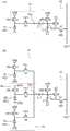
图1是能够用于本发明的一个方式的成像装置的像素电路的电路 图。该像素电路大致被分为光电转换部和信号生成部。为了简化起见, 说明光电转换部包括电路31和电路32的结构。另外,说明信号生成 部包括电路33的结构。此外,说明光电转换部与信号生成部通过电容 元件C-1连接的结构。Fig. 1 is a circuit diagram of a pixel circuit that can be used in an imaging device according to one embodiment of the present invention. The pixel circuit is roughly divided into a photoelectric conversion unit and a signal generation unit. For the sake of simplicity, a configuration in which the photoelectric conversion unit includes the
光电转换部中的电路31包括光电二极管61、晶体管51及晶体管 52。另外,电路32包括光电二极管62、晶体管53及晶体管54。The
作为光电二极管61、62可以采用硅衬底中形成有pn结或pin结的 二极管元件。或者,也可以采用使用非晶硅膜或微晶硅膜等的pin结二 极管元件等。注意,例示出电路31及电路32包括光电二极管的结构, 但是电路31及电路32也可以包括其他光电转换元件。例如,也可以 使用二极管连接的晶体管。此外,也可以使用硅、锗、硒等形成利用 光电效果的可变电阻等。As the
另外,也可以采用利用了所谓雪崩倍增(avalanche multiplication) 现象的包含硒的光电转换元件。在该光电转换元件中,可以得到相对 于入射光量的电子放大量大的高灵敏度传感器。In addition, a photoelectric conversion element containing selenium that utilizes a so-called avalanche multiplication phenomenon may also be used. In this photoelectric conversion element, a high-sensitivity sensor having a large amount of electron amplification with respect to the amount of incident light can be obtained.
作为硒类材料,可以使用非晶硒或结晶硒。例如,通过在形成非 晶硒之后进行加热处理,可以得到结晶硒。另外,通过使结晶硒的结 晶粒径小于像素间距,可以减少各像素的特性偏差。As the selenium-based material, amorphous selenium or crystalline selenium can be used. For example, crystalline selenium can be obtained by performing heat treatment after forming amorphous selenium. In addition, by making the crystal grain size of crystalline selenium smaller than the pixel pitch, variation in characteristics of each pixel can be reduced.
信号生成部所包括的电路33包括晶体管55、晶体管56、晶体管 57及电容元件C-2。The
在电路31中,光电二极管61的一个端子与晶体管51的源极和漏 极中的一个及晶体管52的源极和漏极中的一个电连接。晶体管52的 源极和漏极中的另一个与电容元件C-1的一个端子电连接。In
在电路32中,光电二极管62的一个端子与晶体管53的源极和漏 极中的一个及晶体管54的源极和漏极中的一个电连接。晶体管54的 源极和漏极中的另一个与电容元件C-1的一个端子电连接。In
在此,将连接晶体管52的源极和漏极中的另一个、晶体管54的 源极和漏极中的另一个及电容元件C-1的一个端子的每一个的节点称 为第一电荷积蓄部(FD1)。Here, a node connecting the other of the source and the drain of the
在电路33中,晶体管55的源极和漏极中的一个、晶体管56的栅 极及电容元件C-2的一个端子与电容元件C-1的另一个端子电连接。 另外,晶体管56的源极和漏极中的一个与晶体管57的源极和漏极中 的一个电连接。In the
在此,将连接晶体管55的源极和漏极中的另一个、晶体管56的 栅极、电容元件C-2的一个端子及电容元件C-1的另一个端子的每一 个的节点称为第二电荷积蓄部(FD2)。Here, a node connecting the other of the source and the drain of the
电容元件C-1的电容值优选大于电容元件C-2的电容值。此外, 光电二极管61的一个端子、晶体管51的源极和漏极中的一个以及电 容元件C-1的一个端子之间的电容值优选等于光电二极管62的一个端 子、晶体管53的源极和漏极中的一个以及电容元件C-1的一个端子之 间的电容值。The capacitance value of the capacitive element C-1 is preferably larger than the capacitance value of the capacitive element C-2. Further, the capacitance value between one terminal of the
光电二极管61、62的另一个端子与布线VPD电连接。晶体管51、 53的源极和漏极中的另一个与布线VPR电连接。晶体管55的源极和 漏极中的另一个与布线VFR电连接。电容元件C-2的另一个端子与布 线VC电连接。晶体管56的源极和漏极中的另一个与布线VO电连接。 布线VPD和布线VC可以被用作公共布线。在图1的结构中,布线VPR、 布线VFR及布线VO可以被用作公共布线。The other terminals of the
晶体管51、53的栅极与布线PR电连接。晶体管52的栅极与布线 TX1电连接,晶体管54的栅极与布线TX2电连接。晶体管55的栅极 与布线FR电连接。晶体管57的栅极与布线SEL电连接,源极和漏极 中的另一个与布线OUT(输出)电连接。The gates of the
注意,也可以对布线VO供应GND、VSS、VDD等的电位。在此, 电位或电压是相对的。因此,GND不局限于0V。Note that potentials of GND, VSS, VDD, etc. may be supplied to the wiring VO. Here, potential or voltage is relative. Therefore, GND is not limited to 0V.
光电二极管61(PD1)、光电二极管62(PD2)是受光元件并可以 具有生成与入射到像素电路的光对应的电流的功能。晶体管52、54 可以具有控制电荷从光电二极管61、62积蓄在电荷积蓄部(FD1)中 的功能。晶体管51、53可以具有将电荷积蓄部(FD1)的电位复位的功能。晶体管55可以具有将电荷积蓄部(FD2)的电位复位的功能。 晶体管56可以具有将与电荷积蓄部(FD2)的电位对应的信号输出的 功能。晶体管57在读出时控制像素电路的选择的功能。The photodiode 61 (PD1) and the photodiode 62 (PD2) are light-receiving elements and may have a function of generating a current corresponding to light incident on the pixel circuit. The
布线VPR、布线VPD、布线VC、布线VFR及布线VO可以具有 电源线的功能。布线PR、布线TX1、布线TX2、布线FR、布线SEL 及布线OUT可以具有信号线的功能。The wiring VPR, the wiring VPD, the wiring VC, the wiring VFR, and the wiring VO may function as power supply lines. The wiring PR, the wiring TX1, the wiring TX2, the wiring FR, the wiring SEL, and the wiring OUT may function as signal lines.
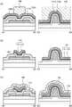
图2A至图2C是说明本发明的一个方式的成像装置所包括的分光 元件与光电转换元件之间的位置关系的示意图。2A to 2C are schematic diagrams illustrating a positional relationship between a spectroscopic element and a photoelectric conversion element included in an imaging apparatus according to one embodiment of the present invention.
图2A示出用来检测出红色(R)的成像数据的两个像素(Pixel-R1 及Pixel-R2)相邻的状态。在此,PD1相当于图1所示的光电二极管 61,PD2相当于光电二极管62。FIG. 2A shows a state in which two pixels (Pixel-R1 and Pixel-R2) for detecting red (R) imaging data are adjacent to each other. Here, PD1 corresponds to the
分光元件65R设置在PD1上。成为成像的对象的光(W:相当于 包括RGB的光成分的白色光)入射到分光元件65R。入射到分光元件 65R的W被分光为以R的波长成分为中心的光(R)和以从W去除以 R的波长成分为中心的光的光(W-R)。The
W-R以在分光元件65R内大致行进的方式从分光元件65R射出到 PD1。另外,R以与W-R不同的角度从分光元件65R射出到PD2。W-R is emitted from the
注意,图2A示出R/2从分光元件65R端在两个方向上射出的情况。 在此情况下,通过合成从作为相邻的像素的Pixel-R2的分光元件65R 射出的R/2,R照射到Pixel-R1的PD2。另外,合成该R和不经过分光 元件65R的W的W+R入射到PD2。Note that FIG. 2A shows a case where R/2 is emitted in both directions from the R end of the spectroscopic element 65 . In this case, R/2 emitted from the
另外,虽然图2A示出R/2从分光元件65R在两个方向上射出的结 构,但是也可以具有如图3A所示的R在一个方向上射出的结构。In addition, although FIG. 2A shows a structure in which R/2 is emitted in two directions from the
图2B示出用来检测出蓝色(B)的数据的两个像素(Pixel-B1及 Pixel-B2)相邻的状态。在此,PD1相当于图1所示的光电二极管61, PD2相当于光电二极管62。FIG. 2B shows a state in which two pixels (Pixel-B1 and Pixel-B2) for detecting blue (B) data are adjacent to each other. Here, PD1 corresponds to the
分光元件65B设置在PD1上。成为成像的对象的入射光(W)入 射到分光元件65B。入射到分光元件65B的W被分光为以B的波长成 分为中心的光(B)和以从W去除以B的波长成分为中心的光的光 (W-B)。The
在图2B中,W-B入射到PD1的说明及W+B入射到PD2的说明 是与用来检测出上述R的成像数据的像素的说明同样的。此外,也可 以采用图3B的结构代替图2B的结构。In Fig. 2B, the description of W-B being incident on PD1 and the description of W+B being incident on PD2 are the same as the description of the pixel for detecting the imaging data of the above-mentioned R. In addition, the structure of Fig. 3B may be used instead of the structure of Fig. 2B.
图2C示出用来检测出绿色(G)的成像数据的两个像素(Pixel-G1 及Pixel-G2)相邻的状态。在此,PD1相当于图1所示的光电二极管 61,PD2相当于光电二极管62。FIG. 2C shows a state in which two pixels (Pixel-G1 and Pixel-G2) for detecting green (G) imaging data are adjacent to each other. Here, PD1 corresponds to the
分光元件65G设置在PD1上。成为成像的对象的光(W:相当于 合成RGB的白色光)入射到分光元件65G。入射到分光元件65G的W 被分光为以R的波长成分为中心的光的一部分(R/2)、以B的波长成 分为中心的光的一部分(B/2)和以从W去除以R/2及B/2的光(W- (R/2)-(B/2))。The
W-(R/2)-(B/2)以在分光元件65R内大致行进的方式从分光元 件65R射出到PD2。另外,R/2及B/2以与W-(R/2)-(B/2)不同的 角度从分光元件65G射出。例如,如图2C所示,从Pixel-G1的分光 元件65G射出的R/2被入射到Pixel-G1的PD1,B/2被入射到相邻的 Pixel-G2的PD1。或者,如图3C所示,也可以具有R/2及B/2在相同 的方向上从分光元件65G射出的结构。W-(R/2)-(B/2) is emitted from the
注意,虽然作为用来获得R或B的成像数据的方式说明图2A和 图2B及图3A和图3B,但是通过改变分光元件,也可以实现用来获得 G的成像数据的方式。此外,虽然作为用来获得G的成像数据的方式 说明图2C和图3C,但是通过改变分光元件,也可以实现用来获得R或B的成像数据的方式。Note that although FIGS. 2A and 2B and FIGS. 3A and 3B are described as means for obtaining imaging data of R or B, the means for obtaining imaging data of G can also be realized by changing the spectroscopic element. In addition, although Figs. 2C and 3C are described as the means for obtaining the imaging data of G, the means for obtaining the imaging data of R or B can also be realized by changing the spectroscopic element.
图4A和图4B是像素的顶面的方式的一个例子。虽然图4A示出 图2A或图3A所示的用来获得R的成像数据的像素,但是图2B或图 3B所示的用来获得B的成像数据的像素也可以具有相同的结构。4A and 4B are an example of the manner of the top surface of the pixel. Although FIG. 4A shows the pixels used to obtain the imaging data of R shown in FIG. 2A or FIG. 3A, the pixels used to obtain the imaging data of B shown in FIG. 2B or 3B may also have the same structure.
因为在本发明的一个方式中利用从PD1及PD2输出的信号的差 分,所以两者的电特性优选相同。也就是说,PD1及PD2优选具有相 同的结构。注意,只要两者的电特性相同,则其结构也可以不同。Since the difference of the signals output from PD1 and PD2 is used in one embodiment of the present invention, the electrical characteristics of both are preferably the same. That is, PD1 and PD2 preferably have the same structure. Note that as long as the electrical characteristics of the two are the same, their structures may also be different.
分光元件65R配置在PD1的中央附近的上方,从分光元件65R分 光的以R的波长成分为中心的光在设置有PD2的方向上射出。像素是 微型像素,在照射到像素整体的外部光中,大致相同量的光被入射到 PD1的上方及PD2的上方。入射到PD1的上方的光被分光元件65R引 入而分光为W-R及R。因此,在图2A的结构中,W-R被入射到PD1, R/2被入射到PD2和与此相邻的像素的PD2的每一个。在图3A的结 构中,R被入射到相同像素的PD2。The
图4B是图2C或图3C所示的用来获得G的成像数据的像素。分 光元件65R配置在PD2的中央附近的上方,从分光元件65G分光的以 R及B的波长成分为中心的光在设置有PD1的方向上射出。与用来获 得R的成像数据的像素同样,大致相同量的光被入射到PD1的上方及PD2的上方。入射到PD2的上方的光被图4B所示的区域66引入,入 射到该区域的光的一半分被入射到分光元件65G。也就是说,从分光 元件65G射出的以R及B的波长成分为中心的光为R/2及B/2。因此, 在图2C的结构中,W-(R/2)-(B/2)被入射到PD2,R/2及B/2分别 被入射到PD1和与此相邻的像素的PD1。在图3C的结构中,R/2及 B/2被入射到相同像素的PD1。FIG. 4B is the pixel used to obtain the imaging data of G shown in FIG. 2C or FIG. 3C . The
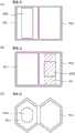
注意,虽然图4A和图4B示出像素、光电二极管及分光元件的顶 面形状为矩形的方式,但是不局限于此。上述构成要素的顶面形状也 可以为圆形、六角形等的多角形等。例如,如图4C所示的图4A的变 形例子那样,像素也可以为两个六角形相邻的多角形,光电二极管也 可以为大致六角形,分光元件也可以为大致圆形。此外,上述矩形、 六角形等的多角形的构成要素所包括的角部也可以具有曲率。Note that although FIGS. 4A and 4B illustrate the manner in which the top surfaces of the pixels, photodiodes, and light-splitting elements are rectangular in shape, they are not limited to this. The shape of the top surface of the above-mentioned constituent elements may be a circle, a polygon such as a hexagon, or the like. For example, as in the modification example of FIG. 4A shown in FIG. 4C , the pixel may be a polygon with two adjacent hexagons, the photodiode may be substantially hexagonal, and the dichroic element may be substantially circular. In addition, the corners included in the above-mentioned polygonal components such as a rectangle and a hexagon may have a curvature.
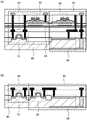
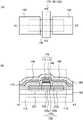
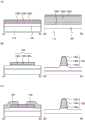
图5A是用来获得R的成像数据的像素的截面的一个例子。PD1 及PD2隔着元件分离层1500分离,在元件分离层1500上设置有防止 混色的遮光层1510。在光电二极管(PD1、PD2)上设置有对可见光具 有高透光性的绝缘层1520,在绝缘层1520上以与光电二极管成对的方 式设置有微透镜1540。FIG. 5A is an example of a cross section of a pixel used to obtain imaging data of R. FIG. PD1 and PD2 are separated via an
并且,在经过微透镜1540的光的光路上设置有分光元件65R。对 分光元件65R的种类没有限制,例如可以使用棱镜或衍射光栅等光学 元件。另外,也可以作为分光元件使用对可见光具有透光性的高折射 率的板状体等。例如,可以使用氮化硅膜等形成该高折射率的板状体。 此外,也可以组合分光元件和其他构成要素。例如,也可以组合棱镜、 衍射光栅、高折射率的板状体等分光元件和镜子、导光板等构成要素。In addition, a
作为一个例子,图5B示出组合分光元件65R和镜子67的方式。 通过使用镜子67,可以提高从分光元件65R射出的光的光路的自由度。 此外,镜子可以使用金属等反射率高的材料形成,也可以具有组合折 射率不同的材料而引起全反射的结构。另外,图42是图5B中的像素 的俯视图的一个例子。As an example, FIG. 5B shows a manner of combining the
另外,如图5C所示,在光电二极管上也可以设置微透镜1541。In addition, as shown in FIG. 5C, a
注意,虽然在图5A、图5B及图5C中说明用来获得R的成像数 据的像素,但是用来获得B的成像数据的像素及用来获得G的成像数 据的像素也可以具有相同的结构。另外,对上述像素的结构没有限制, 也可以具有上述之外的绝缘层、上述之外的遮光层、钝化层膜、粘合 层、抗反射膜、光吸收层等。另外,也可以在微透镜1540与光电二极 管(PD1、PD2)之间包括着色层。Note that although the pixels used to obtain the imaging data of R are described in FIGS. 5A , 5B and 5C, the pixels used to obtain the imaging data of B and the pixels used to obtain the imaging data of G may also have the same structure . In addition, the structure of the above-mentioned pixel is not limited, and may have an insulating layer other than the above, a light shielding layer other than the above, a passivation layer film, an adhesive layer, an antireflection film, a light absorption layer, and the like. In addition, a coloring layer may be included between the
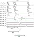
接着,说明包括图1所示的电路的用来获得R的成像数据的像素 的工作。图6A是说明该像素的工作的时序图。在此,布线VPD为低 电位,布线VPR为高电位,布线VC为低电位,布线VFR为高电位, 布线VO为高电位。Next, the operation of the pixel including the circuit shown in Fig. 1 for obtaining imaging data of R will be described. FIG. 6A is a timing chart illustrating the operation of the pixel. Here, the wiring VPD is at a low potential, the wiring VPR is at a high potential, the wiring VC is at a low potential, the wiring VFR is at a high potential, and the wiring VO is at a high potential.
在时刻T1至时刻T2,将布线PR设定为“H”(“高”),将布线FR 设定为“H”,将布线TX1设定为“H”,将布线TX2设定为“H”。此 时,节点FD2的电位被设定为布线VFR的电位,节点FD1的电位被 设定为布线VPR的电位(复位工作)。From time T1 to time T2, the wiring PR is set to "H" ("High"), the wiring FR is set to "H", the wiring TX1 is set to "H", and the wiring TX2 is set to "H" ". At this time, the potential of the node FD2 is set to the potential of the wiring VFR, and the potential of the node FD1 is set to the potential of the wiring VPR (reset operation).
在时刻T2至时刻T3,将布线PR设定为“L”(“低”),将布线FR 设定为“H”,将布线TX1设定为“H”,将布线TX2设定为“L”。此 时,与照射到光电二极管61(PD1)的光,即W-R的光强度(I(W-R)) 成正比,节点FD1的电位下降ΔV1’(参照算式1,α’为比例系数)。 另外,照射到光电二极管61(PD1)的光越强,节点FD1的电位的下 降越快(积蓄工作1)。From time T2 to time T3, the wiring PR is set to "L" ("low"), the wiring FR is set to "H", the wiring TX1 is set to "H", and the wiring TX2 is set to "L" ". At this time, the potential of the node FD1 decreases by ΔV1' (refer to
[算式1][Equation 1]
ΔV1′=α′·(W-R) (1)ΔV1′=α′·(W-R) (1)
在时刻T3,将布线FR设定为“L”,将布线TX1设定为“L”。此 时,节点FD2的电位保持为布线VPR的电位。另外,节点FD1的电 位保持为从布线VPR的电位下降ΔV1’的电位。At time T3, the wiring FR is set to "L", and the wiring TX1 is set to "L". At this time, the potential of the node FD2 is kept at the potential of the wiring VPR. In addition, the potential of the node FD1 is kept at a potential lower by ?V1' from the potential of the wiring VPR.
在时刻T4至时刻T5,将布线PR设定为“H”。此时,光电二极 管61(PD1)的阴极的电位及光电二极管62(PD2)的阴极的电位被 设定为布线VPR的电位(复位工作2)。在时刻T3至时刻T5,因为光 电二极管61(PD1)及光电二极管62(PD2)的阴极的电位下降,所 以优选在时刻T5(将布线TX1及布线TX2设定为“H”)之前将阴极 的电位设定为布线VPR的电位。由此,不发生刚在时刻T5之后节点 FD1的电位急速下降的现象,即噪声的现象,从而能够高精度地取得 成像数据。From time T4 to time T5, the wiring PR is set to "H". At this time, the potential of the cathode of the photodiode 61 (PD1) and the potential of the cathode of the photodiode 62 (PD2) are set to the potential of the wiring VPR (reset operation 2). From time T3 to time T5, since the potentials of the cathodes of the photodiode 61 ( PD1 ) and the photodiode 62 ( PD2 ) drop, it is preferable to set the cathodes of the photodiodes 61 ( PD1 ) and 62 ( PD2 ) before time T5 (setting the wiring TX1 and the wiring TX2 to “H”). The potential is set to the potential of the wiring VPR. As a result, the phenomenon that the potential of the node FD1 drops rapidly immediately after the time T5, that is, the phenomenon of noise does not occur, and imaging data can be acquired with high accuracy.
另外,为了获得同样的效果,优选使电容元件C-1的电容值充分 大于光电二极管61(PD1)的阴极的电容值及光电二极管62(PD2) 的阴极的电容值。In order to obtain the same effect, the capacitance value of the capacitive element C-1 is preferably sufficiently larger than the capacitance value of the cathode of the photodiode 61 (PD1) and the capacitance value of the cathode of the photodiode 62 (PD2).
在时刻T5至时刻T6,将布线PR设定为“H”,将布线FR设定为 “L”,将布线TX1设定为“H”,将布线TX2设定为“H”。此时,节 点FD1的电位被设定为布线VPR的电位。也就是说,节点FD1的电 位比时刻T3至时刻T4高ΔV1’。在此,节点FD2的电位由于电容元件 C-1的电容C1与电容元件C-2的电容C2及晶体管56的栅极电容Cg 的合成电容的电容耦合而上升ΔV1(参照算式2,α为比例系数)。From time T5 to time T6, the wiring PR is set to "H", the wiring FR is set to "L", the wiring TX1 is set to "H", and the wiring TX2 is set to "H". At this time, the potential of the node FD1 is set to the potential of the wiring VPR. That is, the potential of the node FD1 is higher by ?V1' from the time T3 to the time T4. Here, the potential of the node FD2 rises by ΔV1 due to the capacitive coupling of the capacitance C1 of the capacitive element C-1 and the combined capacitance of the capacitance C2 of the capacitive element C-2 and the gate capacitance Cg of the transistor 56 (refer to
[算式2][Equation 2]

在时刻T6至时刻T7,将布线PR设定为“L”,将布线FR设定为 “L”,将布线TX1设定为“L”,将布线TX2设定为“H”。此时,与 照射到光电二极管62(PD2)的光,即W+R的光强度(I(W+R))成 正比,节点FD1的电位下降ΔV2’(参照算式3)。另外,照射到光电二 极管62(PD2)的光越强,节点FD1的电位越低(积蓄工作2)。From time T6 to time T7, the wiring PR is set to "L", the wiring FR is set to "L", the wiring TX1 is set to "L", and the wiring TX2 is set to "H". At this time, in proportion to the light irradiated to the photodiode 62 (PD2), that is, the light intensity of W+R (I(W+R)), the potential of the node FD1 drops by ?V2' (see Equation 3). In addition, the stronger the light irradiated to the photodiode 62 (PD2), the lower the potential of the node FD1 (accumulation operation 2).
[算式3][Equation 3]
ΔV2′=α′·I(W+R) (3)ΔV2′=α′·I(W+R) (3)
此外,节点FD2的电位下降ΔV2(参照算式4)。也就是说,节点 FD2的电位是比布线VFR的电位低ΔV2-ΔV1的电位。在此,如果满足 算式5,则满足ΔV2-ΔV1=2αIR(参照算式6),由此节点FD2的电位 为依赖于入射光W的R成分的电位。In addition, the potential of the node FD2 drops by ΔV2 (see Equation 4). That is, the potential of the node FD2 is lower than the potential of the wiring VFR by ΔV2-ΔV1. Here, when Equation 5 is satisfied, ΔV2 - ΔV1 = 2αIR (see Equation 6) is satisfied, whereby the potential of the node FD2 becomes the potential depending on the R component of the incident light W.
[算式4][Equation 4]

[算式5][Equation 5]
I(W+R)-I(W-R)=I(2R)=2I(R) (5)I(W+R)-I(W-R)=I(2R)=2I(R) (5)
[算式6][Equation 6]
ΔV2-ΔV1=α·I(W+R)-α·I(W-R)=2αI(R) (6)ΔV2-ΔV1=α·I(W+R)-α·I(W-R)=2αI(R) (6)
在时刻T8至时刻T9,将布线SEL设定为“H”(选择工作)。此 时,与节点FD2的电位对应的电位被输出到布线OUT。也就是说,入 射光W的R成分的光强度越强,布线OUT的电位越高。From time T8 to time T9, the wiring SEL is set to "H" (select operation). At this time, the potential corresponding to the potential of the node FD2 is output to the wiring OUT. That is, the stronger the light intensity of the R component of the incident light W, the higher the potential of the wiring OUT.
虽然作为用来获得R的成像数据的工作说明上述内容,但是用来 获得B的成像数据的工作也可以同样地进行。Although the above has been described as the work for obtaining the imaging data of R, the work for obtaining the imaging data of B can be performed in the same way.
接着,说明用来获得G的成像数据的像素的工作。图6B是说明 该像素的工作的时序图。在用来获得G的成像数据的像素中,W+(R/2) +(B/2)被入射到光电二极管61(PD1),W-(R/2)-(B/2)被入射 到光电二极管62(PD2)。Next, the operation of the pixel for obtaining the imaging data of G will be described. Fig. 6B is a timing chart illustrating the operation of the pixel. Among the pixels used to obtain the imaging data of G, W+(R/2)+(B/2) is incident on the photodiode 61 (PD1), and W-(R/2)-(B/2) is incident on the photodiode 61 (PD1) Photodiode 62 (PD2).
图6B的时序图的与图6A的时序图不同之处是:时刻T6至时刻 T7的期间为时刻T2至时刻T3的3倍(A:B=1:3)。也就是说,图6A的说明中的ΔV1及ΔV2可以替换为算式7、算式8。The timing chart of FIG. 6B differs from the timing chart of FIG. 6A in that the period from time T6 to time T7 is three times as long as from time T2 to time T3 (A:B=1:3). That is, ΔV1 and ΔV2 in the description of FIG. 6A may be replaced by Expressions 7 and 8.
[算式7][Equation 7]

[算式8][Equation 8]

因此,节点FD2的电位是比布线VFR的电位低ΔV2-ΔV1的电位。 在此,如果满足算式9,则满足ΔV2-ΔV1=2αIG(参照算式10),由此 节点FD2的电位为依赖于入射光W的G成分的电位。Therefore, the potential of the node FD2 is lower than the potential of the wiring VFR by ΔV2-ΔV1. Here, when Equation 9 is satisfied, ΔV2 - ΔV1 = 2αIG (refer to Equation 10) is satisfied, whereby the potential of the node FD2 becomes the potential depending on the G component of the incident light W.
[算式9][Equation 9]

[算式10][Equation 10]

注意,虽然在上述说明中通过调整期间而调整受光量,但是也可 以通过调整光电二极管的受光面积而调整受光量。例如,通过以受光 面积为PD1:PD2=1:3且满足A:B=1:1的方式进行工作,可以获得G的 成像数据。Note that, although the amount of received light is adjusted by adjusting the period in the above description, the amount of received light may also be adjusted by adjusting the light-receiving area of the photodiode. For example, imaging data of G can be obtained by operating so that the light-receiving area is PD1:PD2=1:3 and A:B=1:1 is satisfied.
可以采用如下结构:由读出电路中的A/D转换电路将布线OUT的 数据转换为数字数据,然后作为图像数据输出该数字数据。注意,虽 然也可以采用由像素外的读出电路进行差分运算的结构,但是通过在 像素内进行差分运算,容易延长曝光时间。A configuration may be adopted in which the data of the wiring OUT is converted into digital data by the A/D conversion circuit in the readout circuit, and then the digital data is output as image data. Note that a configuration in which the difference operation is performed by a readout circuit outside the pixel can also be employed, but by performing the difference operation within the pixel, the exposure time can be easily extended.
另外,优选的是,作为构成像素的晶体管的一部分或全部,使用 包含关态电流(off-state current)优良的氧化物半导体的晶体管。通过 使用该晶体管,可以构成电荷保持特性高的像素。在上述结构中容易 保持减法数据,由此上述结构适于在像素内进行差分运算的结构。In addition, it is preferable to use a transistor including an oxide semiconductor excellent in off-state current as part or all of the transistors constituting the pixel. By using this transistor, a pixel having high charge retention characteristics can be formed. The subtraction data is easily held in the above-described structure, and thus the above-described structure is suitable for a structure in which the difference operation is performed within the pixel.
另外,当将包含氧化物半导体的晶体管用于像素电路时,可以扩 大成像的动态范围。在图1所示的电路结构中,在入射到光电二极管 61、62的光的强度较大时,节点FD1的电位较低。由于使用氧化物半 导体的晶体管的关态电流极低,因此即使栅极电位极小也可以正确地 输出对应于该栅极电位的电流。由此,可以扩大能够检测出的照度范 围,即扩大动态范围。In addition, when a transistor including an oxide semiconductor is used for a pixel circuit, the dynamic range of imaging can be expanded. In the circuit configuration shown in Fig. 1, when the intensity of light incident on the
由于包含氧化物半导体的晶体管具有关态电流较小的特性,可以 在极长的时间内保持节点FD1及节点FD2的电荷。因此,可以适用全 局快门方式,其中不使电路结构或工作方法为复杂地适用在全像素中 同时进行电荷的存储工作。因此,即使在拍摄对象为运动物体的情况 下也可以容易地获得畸变较小的图像。另外,通过采用全局快门方式, 也可以延长曝光时间(进行电荷的储存工作的期间),由此适于低照度 环境下的成像。Since a transistor including an oxide semiconductor has a characteristic of having a small off-state current, the charges at the nodes FD1 and FD2 can be held for an extremely long period of time. Therefore, it is possible to apply a global shutter method in which the circuit structure or operation method is not complicatedly adapted to simultaneously perform charge storage operation in all pixels. Therefore, an image with less distortion can be easily obtained even when the subject is a moving object. In addition, by adopting the global shutter method, the exposure time (the period during which the electric charge storage operation is performed) can be extended, which is suitable for imaging in a low-light environment.
另外,用来控制节点FD1、节点FD2的电位的晶体管等被要求其 噪音少的晶体管。使用后面所述的包含两层或三层的氧化物半导体层 的晶体管的沟道是埋入型沟道,并且该晶体管具有极高的抗噪声性能。 因此,通过使用该晶体管可以得到噪音少的图像。In addition, transistors for controlling the potentials of the node FD1 and the node FD2 are required to have less noise. The channel of the transistor using the later-described oxide semiconductor layer comprising two or three layers is a buried type channel, and the transistor has extremely high noise immunity. Therefore, images with less noise can be obtained by using this transistor.
根据上述本发明的一个方式,能够从入射光W取得R、G、B的 每个成分的成像数据。注意,虽然在上述说明中示出利用使用对R及 B进行分光的分光元件根据差分检测求得G的方式,但是也可以采用 利用使用对R及G进行分光的分光元件根据差分检测求得B的方式。另外,也可以采用利用使用对B及G进行分光的分光元件根据差分检 测求得R的方式。According to one aspect of the present invention described above, from the incident light W, imaging data for each of the components of R, G, and B can be acquired. Note that although the above description shows the method of obtaining G by differential detection using a spectroscopic element that splits R and B, it is also possible to obtain B by differential detection using a spectroscopic element that splits R and G. The way. Alternatively, R may be obtained by differential detection using a spectroscopic element that splits B and G.
此外,如图40A所示,能够用于本发明的一个方式的成像装置的 像素电路也可以具有使用一个电路31构成光电转换部的方式。在此情 况下,通过将图1的电路的工作的说明中的照射到PD1的光和照射到 PD2的光交替地照射到图40A所示的PD1,可以得到各颜色的成像数 据。Further, as shown in Fig. 40A , a pixel circuit that can be used in an imaging device according to one embodiment of the present invention may have a mode in which a photoelectric conversion section is configured using one
另外,也可以采用光电转换部包括三个以上的电路的结构。例如, 在图40B所示的像素电路中,光电转换部包括电路31、电路32及电 路34,该电路34包括光电二极管63(PD3)、晶体管58及晶体管59。In addition, a structure in which the photoelectric conversion unit includes three or more circuits may be employed. For example, in the pixel circuit shown in FIG. 40B , the photoelectric conversion section includes a
此外,如图7A所示,在能够用于本发明的一个方式的成像装置的 像素电路中,光电二极管的连接方向也可以与图1所示的电路不同。 在此情况下,布线VPD为高电位,布线VPR为低电位,布线VC为低 电位,布线VFR为高电位,布线VO为高电位。In addition, as shown in Fig. 7A , in a pixel circuit that can be used in an imaging device according to one embodiment of the present invention, the connection direction of the photodiodes may be different from the circuit shown in Fig. 1 . In this case, the wiring VPD is at a high potential, the wiring VPR is at a low potential, the wiring VC is at a low potential, the wiring VFR is at a high potential, and the wiring VO is at a high potential.
关于用来获得R及B的成像数据的像素的工作,可以与图6A所 示的时序图同样地输入信号,FD1及FD2的电位如图7B的时序图所 示那样变化。在时刻T7,节点FD2的电位是比布线VFR的电位高 ΔV2-ΔV1的电位。另外,为了获得G的成像数据,与图6B的时序图 同样,图7B的时序图也可以将时刻T6至时刻T7的期间设定为时刻 T2至时刻T3的三倍。或者,可以将光电二极管的受光面积设定为 PD1:PD2=1:3。Regarding the operation of the pixels for obtaining R and B imaging data, signals can be input in the same manner as in the timing chart shown in Fig. 6A, and the potentials of FD1 and FD2 are changed as shown in the timing chart of Fig. 7B. At time T7, the potential of the node FD2 is higher than the potential of the wiring VFR by ΔV2-ΔV1. In order to obtain the imaging data of G, the time chart of FIG. 7B may set the period from time T6 to time T7 three times as long as from time T2 to time T3 in the same way as the time chart of FIG. 6B . Alternatively, the light-receiving area of the photodiode can be set to PD1:PD2=1:3.
此外,如图8所示,能够用于本发明的一个方式的成像装置的像 素电路也可以采用从图1所示的电路去除晶体管51及晶体管53的结 构。在此情况下,布线VC为低电位,布线VFR为高电位,布线VO 为高电位。另外,布线PR也可以被用作电源线。In addition, as shown in Fig. 8 , the pixel circuit that can be used in the imaging apparatus according to one embodiment of the present invention may have a configuration in which the
在此情况下,通过将布线PR设定为高电位,可以进行节点FD1 的复位工作。当在预定期间将布线PR设定为高电位时,PD1、PD2被 施加正向偏压。在该期间,通过将TX1、TX2设定为“H”,可以将节 点FD1设定为布线PR的电位。另外,当在预定期间将布线PR设定为 低电位时,PD1、PD2被施加反向偏压。在该期间,通过将TX1、TX2 设定为“H”,可以进行积蓄工作。另外,在这些工作中可以使用图6A 和图6B所示的时序图。In this case, the reset operation of the node FD1 can be performed by setting the wiring PR to a high potential. When the wiring PR is set to a high potential for a predetermined period, the forward bias voltages are applied to PD1 and PD2. During this period, by setting TX1 and TX2 to "H", the node FD1 can be set to the potential of the wiring PR. In addition, when the wiring PR is set to a low potential for a predetermined period, reverse bias is applied to PD1 and PD2. During this period, the accumulation operation can be performed by setting TX1 and TX2 to "H". In addition, the timing diagrams shown in FIGS. 6A and 6B may be used in these operations.
另外,如图41A所示,作为图8所示的像素电路的结构,也可以 使用一个电路31构成光电转换部。另外,如图41B所示,也可以使用 三个以上的电路构成光电转换部。In addition, as shown in Fig. 41A, as the structure of the pixel circuit shown in Fig. 8, a photoelectric conversion portion may be constituted using one
另外,作为用来获得上述R、G、B的成像数据的像素的排列,例 如可以采用图9A和图9B所示的方式。图9A和图9B示出3×3的像素 的顶面方式的一个例子,对RGB的顺序没有限制。在用来获得R及B 的成像数据的像素中,在分光元件的符号的下侧设置有PD1。另外,在用来获得G的成像数据的像素中,在分光元件的符号的下侧设置有 PD2。In addition, as the arrangement of pixels for obtaining the imaging data of R, G, and B described above, for example, the methods shown in Figs. 9A and 9B can be adopted. Fig. 9A and Fig. 9B show an example of the top surface method of 3x3 pixels, and the order of RGB is not limited. In the pixels for obtaining the imaging data of R and B, PD1 is provided on the lower side of the symbol of the spectroscopic element. In addition, in the pixel for obtaining the imaging data of G, PD2 is provided on the lower side of the symbol of the spectroscopic element.
另外,也可以采用使用滤色片对R、G、B中的任何一个成分进行 分光的结构。图9C是一个例子,是在用来获得R的成像数据的像素上 设置滤色片(R)的方式。另外,也可以采用使用滤色片对R、G、B 中的任何两个成分进行分光的结构。图9D是一个例子,是在用来获得 R及G的成像数据的像素上分别设置滤色片(R)、滤色片(G)的方 式。通过采用上述结构,容易制造分光元件或滤色片,从而容易实现 微型化、低成本化。In addition, it is also possible to adopt a structure in which any one of R, G, and B components is spectrally separated using a color filter. Fig. 9C is an example of the manner in which color filters (R) are provided on pixels used to obtain R imaging data. In addition, it is also possible to adopt a structure in which any two components of R, G, and B are spectrally separated using a color filter. Fig. 9D is an example of a method in which a color filter (R) and a color filter (G) are provided on pixels for obtaining R and G imaging data, respectively. By adopting the above-mentioned structure, the spectroscopic element or the color filter can be easily manufactured, and miniaturization and cost reduction can be easily achieved.
注意,虽然在图9A至图9D中示出在纵方向上排列RGB的方式, 但是也可以采用在横方向上排列RGB的方式。此外,如图9E所示, 也可以采用包括半个间距错开的像素的结构。图9E的结构也可以应用 于包括滤色片的结构。Note that although the manner of arranging RGB in the vertical direction is shown in FIGS. 9A to 9D, a manner of arranging RGB in the horizontal direction may also be employed. In addition, as shown in FIG. 9E, a structure including pixels staggered by a half pitch may also be employed. The structure of Fig. 9E can also be applied to a structure including color filters.
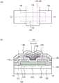
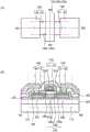
图10A示出包括电路部的成像装置的截面图的一个例子。电路部 90是在硅衬底中具有活性区域的晶体管51和将氧化物半导体用作活 性层的晶体管52的组合,例如可以构成反相器电路或存储电路等。电 路部92是使用硅衬底40形成的光电二极管60和将氧化物半导体用作 活性层的晶体管56的组合,例如能够构成图1所示的电路31或电路 32等。注意,以虚线表示的布线及接触插头表示其深度方向上的位置 与其他布线及接触插头不同。FIG. 10A shows an example of a cross-sectional view of an imaging device including a circuit portion. The
在此,电路部92相当于图1所示的光电转换部的一部分,光电二 极管60相当于图1所示的光电二极管61或光电二极管62。另外,晶 体管56相当于图1所示的晶体管51或晶体管53。Here, the
在图10A中,可以将光电二极管60与晶体管56重叠地形成,因 此可以提高像素的集成度。换而言之,可以提高成像装置的分辨率。 此外,在电路部92所占的区域中硅衬底40中没有形成晶体管,由此 可以扩大光电二极管的面积。因此,即使在低照度环境下也可以得到 噪音少的图像。In Fig. 10A, the
注意,图10A和图10B示出使用同一硅衬底40形成光电二极管 60和晶体管51的结构,但是不局限于此,例如也可以使用硅衬底40 形成晶体管51,并对晶体管51贴合使用其他衬底形成的光电二极管。 另外,也可以不使用硅衬底40形成晶体管51,而与晶体管52、晶体 管56同样地,使用将氧化物半导体用作活性层的晶体管作为晶体管 51。如图10B所示,可以使用硅衬底40设置晶体管51、晶体管52、 晶体管56(未图示晶体管52)。晶体管51以外的元件也可以使用硅衬 底40形成。例如,可以使用硅衬底40形成电容元件、二极管、电阻元件等。Note that FIGS. 10A and 10B show a structure in which the
另外,当图10A所示的结构包括晶体管51及光电二极管60时, 在晶体管52与晶体管56之间设置有绝缘层80。In addition, when the structure shown in FIG. 10A includes the
设置在晶体管51的活性区域附近的绝缘层中的氢使硅的悬空键终 结。因此,该氢具有提高晶体管51的可靠性的效果。另一方面,设置 在晶体管52及晶体管56等的活性层的氧化物半导体层附近的绝缘层 中的氢成为氧化物半导体中生成载流子的主要原因之一。因此,该氢 有可能引起晶体管52及晶体管56等的可靠性的下降。因此,当层叠 包含使用硅类半导体材料的晶体管的一个层与包含使用氧化物半导体 的晶体管的另一个层时,优选在它们之间设置具有防止氢扩散的功能 的绝缘层80。通过设置绝缘层80将氢封闭在一个层中,可以提高晶体 管51的可靠性。同时,由于能够抑制氢从一个层扩散到另一个层,所以可以同时提高晶体管52及晶体管56等的可靠性。The hydrogen provided in the insulating layer near the active region of
绝缘层80例如可以使用氧化铝、氧氮化铝、氧化镓、氧氮化镓、 氧化钇、氧氮化钇、氧化铪、氧氮化铪、氧化钇稳定氧化锆(YSZ) 等。For the insulating
作为硅衬底40不局限于块硅衬底,也可以使用SOI衬底。此外, 也可以使用以锗、硅锗、碳化硅、砷化镓、砷化铝镓、磷化铟、氮化 镓、有机半导体为材料的衬底代替硅衬底40。The
注意,晶体管51不局限于平面型晶体管而可以采用各种类型的晶 体管。例如,可以是FIN(鳍)型、TRI-GATE(三栅)型晶体管等。Note that the
根据情况,晶体管56除了氧化物半导体以外还可以包含各种半导 体。此外,也可以包含硅、锗、硅锗、碳化硅、砷化镓、砷化铝镓、 磷化铟、氮化镓、有机半导体等。Depending on the circumstances, the
如图11A1及图11B1所示,可以使成像装置弯曲。图11A1示出 使成像装置在该附图中的双点划线X1-X2的方向上弯曲的状态。图11A2是沿着图11A1中的双点划线X1-X2所示的部分的截面图。图11A3是沿着图11A1中的双点划线Y1-Y2所示的部分的截面图。As shown in FIGS. 11A1 and 11B1 , the imaging device can be bent. Fig. 11A1 shows a state in which the imaging device is bent in the direction of the two-dot chain line X1-X2 in the drawing. FIG. 11A2 is a cross-sectional view of the portion shown along the two-dot chain line X1 - X2 in FIG. 11A1 . FIG. 11A3 is a cross-sectional view of the portion shown along the two-dot chain line Y1 - Y2 in FIG. 11A1 .
图11B1示出使成像装置在该附图中的双点划线X3-X4的方向上 弯曲且在该附图中的双点划线Y3-Y4的方向上弯曲的状态。图11B2是沿着图11B1中的双点划线X3-X4所示的部分的截面图。图11B3是 沿着图11B1中的双点划线Y3-Y4所示的部分的截面图。Fig. 11B1 shows a state in which the imaging device is bent in the direction of the two-dot chain line X3-X4 in the drawing and in the direction of the two-dot chain line Y3-Y4 in the drawing. FIG. 11B2 is a cross-sectional view along the portion shown by the two-dot chain line X3 - X4 in FIG. 11B1 . Fig. 11B3 is a cross-sectional view of the portion shown by the two-dot chain line Y3-Y4 in Fig. 11B1.
通过使成像装置弯曲,可以降低像场弯曲或像散(astigmatism)。 因此,可以使与成像装置组合使用的透镜等的光学设计变容易。例如, 由于可以减少用来进行像差校正的透镜的数量,所以可以容易地实现 使用成像装置的半导体装置等的小型化或轻量化。此外,可以提高成 像图像的质量。By bending the imaging device, field curvature or astigmatism can be reduced. Therefore, the optical design of a lens or the like used in combination with the imaging device can be facilitated. For example, since the number of lenses used for aberration correction can be reduced, miniaturization or weight reduction of semiconductor devices and the like using the imaging device can be easily achieved. Also, the quality of the imaged image can be improved.
注意,在本实施方式中,说明了本发明的一个方式。或者,在其 他的实施方式中,将说明本发明的一个方式。注意,本发明的一个方 式不局限于这些。例如,虽然示出将本发明的一个方式应用于成像装 置的例子,但是本发明的一个方式不局限于此。在一些情况下,或者, 根据情况,也可以不将本发明的一个方式应用于成像装置。例如,可 以将本发明的一个方式应用于具有其他的功能的半导体装置。Note that in the present embodiment, one form of the present invention has been described. Alternatively, in other embodiments, one form of the present invention will be described. Note that one form of the present invention is not limited to these. For example, although an example in which one aspect of the present invention is applied to an image forming apparatus is shown, one aspect of the present invention is not limited to this. In some cases, or depending on the circumstances, one aspect of the present invention may not be applied to an imaging device. For example, one embodiment of the present invention can be applied to a semiconductor device having other functions.
本实施方式可以与其他实施方式所示的结构适当地组合而实施。This embodiment mode can be implemented in combination with the configurations shown in other embodiments as appropriate.
实施方式2
在本实施方式中说明像素电路的驱动方法的一个例子。An example of a driving method of a pixel circuit will be described in this embodiment mode.
如在实施方式1中所说明的那样,像素电路的工作就是反复进行 复位工作、积蓄工作以及选择工作。作为控制整个像素矩阵的成像方 法,已知全局快门方式及卷帘快门方式。As described in the first embodiment, the operation of the pixel circuit is to repeat the reset operation, the accumulation operation, and the selection operation. As an imaging method for controlling the entire pixel matrix, a global shutter method and a rolling shutter method are known.
图12是利用全局快门方式时的时序图。在图12中,以以矩阵状 具有多个像素电路且在该像素电路中具有图1所示的电路的成像装置 为例,对第一行至第n行(n为3以上的自然数)的像素电路的工作进 行说明。FIG. 12 is a timing chart when the global shutter method is used. In FIG. 12 , taking an example of an imaging device having a plurality of pixel circuits in a matrix and including the circuit shown in FIG. 1 in the pixel circuits, the pixel circuits of the first row to the n-th row (n is a natural number of 3 or more) are used as an example. The operation of the pixel circuit will be described.
在图12中,信号501、信号502以及信号503为输入连接于第一 行、第二行以及第n行的各像素电路的布线PR的信号。此外,信号 504、信号506以及信号508为输入连接于第一行、第二行以及第n行 的各像素电路的布线TX1的信号。此外,信号505、信号507以及信 号509为输入连接于第一行、第二行以及第n行的各像素电路的布线 TX2的信号。此外,信号510、信号511以及信号512为输入连接于第 一行、第二行以及第n行的各像素电路的布线SEL的信号。In Fig. 12, a
另外,期间515是一次拍摄所要的期间。期间516是各行的像素 电路同时进行复位工作及积蓄工作的期间。各行的像素电路依次进行 选择工作。作为一个例子,期间517是第一行的像素电路进行选择工 作的期间。如此,在全局快门方式中,在全像素电路大致同时进行复 位工作及积蓄工作,并按行依次进行读出工作。In addition, the
也就是说,在全局快门方式中,由于在所有像素电路中大致同时 进行积蓄工作,因此确保各行的像素电路中的成像的同时性。因此, 即使拍摄对象为运动物体也可以获得畸变小的图像。That is, in the global shutter method, since the accumulation operation is performed in all pixel circuits substantially simultaneously, the simultaneity of imaging in the pixel circuits of each row is ensured. Therefore, even if the subject is a moving object, an image with less distortion can be obtained.
另一方面,图13是使用卷帘快门方式的情况的时序图。关于信号 501至512,可以参照图10A和图10B的说明。期间615是一次拍摄 所要的期间。期间621是第一行的像素进行复位工作及积蓄工作的期 间。期间622是第二行的像素进行复位工作及积蓄工作的期间。期间 623是第n行的像素进行复位工作及积蓄工作的期间。此外,期间617 是第一行的像素电路进行选择工作的期间。如上所述,在卷帘快门方 式中,由于积蓄工作不是在所有像素电路中同时进行,而是按行依次 进行,因此不能确保各行的像素电路之间的成像的同时性。因此,在 第一行与最终行的成像的时序不同,由此在运动物体为拍摄对象时图 像的畸变变大。On the other hand, FIG. 13 is a timing chart in the case of using the rolling shutter method. Regarding the
为了实现全局快门方式,需要直到来自各像素的信号的读出结束 为止长时间保持电荷积蓄部(FD2)的电位。通过将由氧化物半导体形 成沟道形成区域的关态电流极小的晶体管用作晶体管55等,可以长时 间保持电荷积蓄部(FD2)的电位。另一方面,在将由硅等形成沟道形 成区域的晶体管用作晶体管55等时,因为关态电流大所以无法长时间 保持电荷积蓄部(FD2)的电位,因此无法使用全局快门方式。In order to realize the global shutter method, it is necessary to hold the electric potential of the charge storage unit (FD2) for a long time until the readout of the signal from each pixel is completed. The potential of the charge storage portion (FD2) can be maintained for a long period of time by using, as the
如上所述,通过将由氧化物半导体形成沟道形成区域的晶体管用 于像素电路,可以容易实现全局快门方式。As described above, by using a transistor in which a channel formation region is formed of an oxide semiconductor for a pixel circuit, a global shutter method can be easily realized.
本实施方式可以与其他实施方式所记载的结构适当地组合而实 施。The present embodiment can be implemented by appropriately combining the configurations described in the other embodiments.
实施方式3
在本实施方式中,参照附图对能够用于本发明的一个方式的具有 氧化物半导体的晶体管进行说明。在本实施方式的附图中,为了明确 起见,放大、缩小或省略部分构成要素。In this embodiment mode, a transistor having an oxide semiconductor that can be used in one embodiment of the present invention will be described with reference to the drawings. In the drawings of the present embodiment, some constituent elements are enlarged, reduced or omitted for clarity.
图14A及图14B是本发明的一个方式的晶体管101的俯视图及截 面图。图14A是俯视图,图14A所示的点划线B1-B2方向上的截面相 当于图14B。另外,图14A所示的点划线B3-B4方向上的截面相当于 图20A。另外,有时将点划线B1-B2方向称为沟道长度方向,将点划线B3-B4方向称为沟道宽度方向。14A and 14B are a plan view and a cross-sectional view of the
晶体管101包括与衬底115接触的绝缘层120、与绝缘层120接触 的氧化物半导体层130、与氧化物半导体层130电连接的导电层140 及导电层150、与氧化物半导体层130、导电层140及导电层150接触 的绝缘层160、与绝缘层160接触的导电层170、与导电层140、导电 层150、绝缘层160及导电层170接触的绝缘层175以及与绝缘层175 接触的绝缘层180。此外,根据需要也可以对绝缘层180附加平坦化膜 的功能。The
这里,导电层140、导电层150、绝缘层160及导电层170分别可 以用作源电极层、漏电极层、栅极绝缘膜及栅电极层。Here, the
此外,图14B所示的区域231、区域232及区域233分别可以用 作源区域、漏区域及沟道形成区域。区域231与导电层140接触且区 域232与导电层150接触,通过作为导电层140及导电层150使用容 易与氧键合的导电材料可以降低区域231及区域232的电阻。In addition, the
具体而言,由于氧化物半导体层130与导电层140及导电层150 接触,在氧化物半导体层130中产生氧缺损,该氧缺损与残留在氧化 物半导体层130中或从外部扩散的氢之间的相互作用使区域231及区 域232成为低电阻的n型。Specifically, since the
另外,晶体管的“源极”和“漏极”的功能在使用极性不同的晶 体管的情况下或在电路工作中电流方向变化的情况等下,有时互相调 换。因此,在本说明书中,“源极”和“漏极”可以互相调换。此外, “电极层”也可以称为“布线”。In addition, the functions of "source" and "drain" of a transistor may be interchanged with each other when transistors with different polarities are used or when the direction of current changes during circuit operation. Therefore, in this specification, "source" and "drain" may be interchanged with each other. In addition, the "electrode layer" may also be referred to as "wiring".
此外,示出导电层170由导电层171及导电层172的两层形成的 例子,但也可以采用一层或三层以上的叠层。同样也可以应用于本实 施方式所说明的其他晶体管。In addition, the example in which the
此外,示出导电层140及导电层150为单层的例子,但也可以采 用两层以上的叠层。同样也可以应用于本实施方式所说明的其他晶体 管。In addition, the example in which the
此外,本发明的一个方式的晶体管也可以采用图15A及图15B所 示的结构。图15A是晶体管102的俯视图,图15A所示的点划线C1-C2 方向上的截面相当于图15B。另外,图15A所示的点划线C3-C4方向 上的截面相当于图20B。另外,有时将点划线C1-C2方向称为沟道长 度方向,将点划线C3-C4方向称为沟道宽度方向。In addition, the transistor according to one embodiment of the present invention may have the structure shown in Figs. 15A and 15B. FIG. 15A is a plan view of the
晶体管102除了用作栅极绝缘膜的绝缘层160的端部不与用作栅 电极层的导电层170的端部对齐之处以外其他结构与晶体管101相同。 在晶体管102中,由于导电层140及导电层150的较宽的部分由绝缘 层160覆盖,所以在导电层140、导电层150与导电层170之间的电阻 高,因此晶体管102具有栅极泄漏电流小的特征。The
晶体管101及晶体管102是具有导电层170与导电层140及导电 层150重叠的区域的顶栅结构。为了减少寄生电容,优选将该区域的 沟道长度方向上的宽度设定为3nm以上且小于300nm。另一方面,由 于不在氧化物半导体层130中形成偏置区域,所以容易形成通态电流 (on-state current)大的晶体管。The
此外,本发明的一个方式的晶体管也可以采用图16A及图16B所 示的结构。图16A是晶体管103的俯视图,图16A所示的点划线D1-D2 方向上的截面相当于图16B。另外,图16A所示的点划线D3-D4方向 上的截面相当于图20A。另外,有时将点划线D1-D2方向称为沟道长 度方向,将点划线D3-D4方向称为沟道宽度方向。In addition, the transistor according to one embodiment of the present invention may have the structure shown in FIGS. 16A and 16B . FIG. 16A is a plan view of the
晶体管103包括与衬底115接触的绝缘层120、与绝缘层120接触 的氧化物半导体层130、与氧化物半导体层130接触的绝缘层160、与 绝缘层160接触的导电层170、覆盖氧化物半导体层130、绝缘层160 及导电层170的绝缘层175、与绝缘层175接触的绝缘层180、通过设 置在绝缘层175及绝缘层180中的开口部与氧化物半导体层130电连 接的导电层140及导电层150。此外,根据需要也可以包括与绝缘层 180、导电层140及导电层150接触的绝缘层(平坦化膜)等。The
这里,导电层140、导电层150、绝缘层160及导电层170分别可 以用作源电极层、漏电极层、栅极绝缘膜及栅电极层。Here, the
此外,图16B所示的区域231、区域232及区域233分别可以用 作源区域、漏区域及沟道形成区域。区域231及区域232与绝缘层175 接触,例如通过作为绝缘层175使用含氢的绝缘材料可以降低区域231 及区域232的电阻。In addition, the
具体而言,经过直到形成绝缘层175为止的工序在区域231及区 域232中产生的氧缺损与从绝缘层175扩散到区域231及区域232的 氢之间的相互作用使区域231及区域232成为低电阻的n型。此外, 作为含氢的绝缘材料,例如可以使用氮化硅膜、氮化铝膜等。Specifically, the interaction between the oxygen vacancy generated in the
此外,本发明的一个方式的晶体管也可以采用图17A及图17B所 示的结构。图17A是晶体管104的俯视图,图17A所示的点划线E1-E2 方向上的截面相当于图17B。另外,图17A所示的点划线E3-E4方向 上的截面相当于图20A。另外,有时将点划线E1-E2方向称为沟道长 度方向,将点划线E3-E4方向称为沟道宽度方向。In addition, the transistor according to one embodiment of the present invention may have the structure shown in FIGS. 17A and 17B . FIG. 17A is a plan view of the
晶体管104除了导电层140及导电层150重叠于氧化物半导体层 130的端部且与其接触之处以外其他结构与晶体管103相同。The structure of the
此外,图17B所示的区域331及区域334可以用作源区域,区域 332及区域335可以用作漏区域,区域333可以用作沟道形成区域。可 以以与晶体管101中的区域231及区域232相同的方式降低区域331 及区域332的电阻。此外,可以以与晶体管103中的区域231及区域232相同的方式降低区域334及区域335的电阻。另外,当沟道长度方 向上的区域334及区域335的长度为100nm以下,优选为50nm以下 时,栅极电场有助于防止通态电流大幅度地下降,所以也可以采用不 进行上述低电阻化的结构。In addition, the
晶体管103及晶体管104的结构是不具有导电层170与导电层140 及导电层150重叠的区域的自对准结构。自对准结构的晶体管由于栅 电极层与源电极层及漏电极层之间的寄生电容极小,所以适用于高速 工作。The structures of the
此外,本发明的一个方式的晶体管也可以采用图18A及图18B所 示的结构。图18A是晶体管105的俯视图,图18A所示的点划线F1-F2 方向上的截面相当于图18B。另外,图18A所示的点划线F3-F4方向 上的截面相当于图20A。另外,有时将点划线F1-F2方向称为沟道长 度方向,将点划线F3-F4方向称为沟道宽度方向。In addition, the transistor according to one embodiment of the present invention may have the structure shown in FIGS. 18A and 18B . FIG. 18A is a plan view of the
晶体管105包括与衬底115接触的绝缘层120、与绝缘层120接触 的氧化物半导体层130、与氧化物半导体层130电连接的导电层141 及导电层151、与氧化物半导体层130、导电层141及导电层151接触 的绝缘层160、与绝缘层160接触的导电层170、与氧化物半导体层130、 导电层141、导电层151、绝缘层160及导电层170接触的绝缘层175、 与绝缘层175接触的绝缘层180、通过设置在绝缘层175及绝缘层180 中的开口部分别与导电层141及导电层151电连接的导电层142及导 电层152。此外,根据需要也可以具有与绝缘层180、导电层142及导 电层152接触的绝缘层等。The
这里,导电层141及导电层151与氧化物半导体层130的顶面接 触而不与侧面接触。Here, the
除了包括导电层141及导电层151、包括设置在绝缘层175及绝缘 层180中的开口部、通过该开口部分别与导电层141及导电层151电 连接的导电层142及导电层152之处以外,晶体管105具有与晶体管 101相同的结构。可以将导电层140(导电层141及导电层142)用作 源电极层,且可以将导电层150(导电层151及导电层152)用作漏电 极层。Except for the
此外,本发明的一个方式的晶体管也可以采用图19A及图19B所 示的结构。图19A是晶体管106的俯视图,图19A所示的点划线G1-G2 方向上的截面相当于图19B。另外,图19A所示的点划线G3-G4方向 上的截面相当于图20A。另外,有时将点划线G1-G2方向称为沟道长 度方向,将点划线G3-G4方向称为沟道宽度方向。In addition, the transistor according to one embodiment of the present invention may have the structure shown in Figs. 19A and 19B. 19A is a plan view of the
晶体管106包括与衬底115接触的绝缘层120、与绝缘层120接触 的氧化物半导体层130、与氧化物半导体层130电连接的导电层141 及导电层151、与氧化物半导体层130接触的绝缘层160、与绝缘层160 接触的导电层170、与绝缘层120、氧化物半导体层130、导电层141、 导电层151、绝缘层160及导电层170接触的绝缘层175、与绝缘层175 接触的绝缘层180、通过设置在绝缘层175及绝缘层180中的开口部分 别与导电层141及导电层151电连接的导电层142及导电层152。此外, 根据需要也可以具有与绝缘层180、导电层142及导电层152接触的绝 缘层(平坦化膜)等。The
这里,导电层141及导电层151与氧化物半导体层130的顶面接 触而不与侧面接触。Here, the
晶体管106除了包括导电层141及导电层151之处以外其他结构 与晶体管103相同。可以将导电层140(导电层141及导电层142)用 作源电极层,且可以将导电层150(导电层151及导电层152)用作漏 电极层。The structure of the
在晶体管105及晶体管106中,由于导电层140及导电层150不 与绝缘层120接触,所以绝缘层120中的氧不容易被导电层140及导 电层150夺取,可以容易将氧从绝缘层120供应给氧化物半导体层130。In the
此外,也可以对晶体管103中的区域231及区域232、晶体管104 及晶体管106中的区域334及区域335添加用来形成氧缺损来提高导 电率的杂质。作为在氧化物半导体层中形成氧缺损的杂质,例如可以 使用选自磷、砷、锑、硼、铝、硅、氮、氦、氖、氩、氪、氙、铟、 氟、氯、钛、锌及碳中的一种以上。作为该杂质的添加方法,可以使 用等离子体处理法、离子注入法、离子掺杂法、等离子体浸没离子注 入法(Plasma-immersion ion implantationmethod)等。In addition, impurities for forming oxygen vacancies to improve conductivity may be added to
通过将上述元素作为杂质元素添加到氧化物半导体层,氧化物半 导体层中的金属元素与氧之间的键合被切断,形成氧缺损。通过包含 在氧化物半导体层中的氧缺损与残留在氧化物半导体层中或在后面添 加的氢之间的相互作用,可以提高氧化物半导体层的导电率。By adding the above-mentioned element as an impurity element to the oxide semiconductor layer, the bond between the metal element and oxygen in the oxide semiconductor layer is cut, and oxygen deficiency is formed. The conductivity of the oxide semiconductor layer can be improved by the interaction between oxygen vacancies contained in the oxide semiconductor layer and hydrogen remaining in the oxide semiconductor layer or added later.
另外,当对添加杂质元素形成有氧缺损的氧化物半导体添加氢时, 氢进入氧缺损处而在导带附近形成施主能级。其结果是,可以形成氧 化物导电体。另外,这里氧化物导电体是指导电体化的氧化物半导体。In addition, when hydrogen is added to an oxide semiconductor in which an oxygen defect is formed by adding an impurity element, the hydrogen enters the oxygen defect and forms a donor level in the vicinity of the conduction band. As a result, an oxide conductor can be formed. In addition, the oxide conductor here is an oxide semiconductor that guides conductorization.
氧化物导电体是简并半导体,可以推测其导带端与费米能级一致 或大致一致。因此,氧化物导电体层与用作源电极层及漏电极层的导 电层之间得到欧姆接触,可以降低氧化物导电体层与用作源电极层及 漏电极层的导电层之间的接触电阻。Oxide conductors are degenerate semiconductors, and it can be speculated that their conduction band ends coincide or roughly coincide with the Fermi level. Therefore, ohmic contact is obtained between the oxide conductor layer and the conductive layers used as the source electrode layer and the drain electrode layer, and the contact between the oxide conductor layer and the conductive layers used as the source electrode layer and the drain electrode layer can be reduced. resistance.
另外,如图21A至图21F的沟道长度方向的截面图以及图20C及图20D的沟道宽度方向的截面图所示,本发明的一个方式的晶体管也 可以包括氧化物半导体层130与衬底115之间的导电层173。通过将该 导电层用作第二栅电极层(背栅极),能够进一步增加通态电流或控制 阈值电压。此外,在图21A至图21F所示的截面图中,也可以使导电 层173的宽度比氧化物半导体层130小。再者,也可以使导电层173 的宽度比导电层170小。In addition, as shown in cross-sectional views in the channel length direction in FIGS. 21A to 21F and cross-sectional views in the channel width direction in FIGS. 20C and 20D , the transistor according to one embodiment of the present invention may include an
当想要增加通态电流时,例如,对导电层170及导电层173供应 相同的电位来实现双栅晶体管即可。另外,当想要控制阈值电压时, 对导电层173供应与导电层170不同的恒电位即可。为了对导电层170 及导电层173供应相同的电位,例如,如图20D所示,通过接触孔使 导电层170与导电层173电连接即可。When it is desired to increase the on-state current, for example, a double-gate transistor may be realized by supplying the same potential to the
此外,在图14A至图19B的晶体管101至晶体管106中示出氧化 物半导体层130为单层的例子,但是氧化物半导体层130也可以为叠 层。晶体管101至晶体管106的氧化物半导体层130可以与图22A至 图22C或图23A至图23C所示的氧化物半导体层130调换。In addition, in the
图22A至图22C是两层结构的氧化物半导体层130的俯视图及截 面图。图22A是俯视图,图22A所示的点划线A1-A2方向上的截面相 当于图22B。另外,图22A所示的点划线A3-A4方向上的截面相当于 图22C。22A to 22C are a plan view and a cross-sectional view of the
图23A至图23C是三层结构的氧化物半导体层130的俯视图及截 面图。图23A是俯视图,图23A所示的点划线A1-A2方向上的截面相 当于图23B。另外,图23A所示的点划线A3-A4方向上的截面相当于 图23C。23A to 23C are a plan view and a cross-sectional view of the
作为氧化物半导体层130a、氧化物半导体层130b、氧化物半导体 层130c可以使用其组成彼此不同的氧化物半导体层等。As the
此外,本发明的一个方式的晶体管也可以采用图24A及图24B所 示的结构。图24A是晶体管107的俯视图,图24A所示的点划线H1-H2 方向上的截面相当于图24B。另外,图24A所示的点划线H3-H4方向 上的截面相当于图30A。另外,有时将点划线H1-H2方向称为沟道长 度方向,将点划线H3-H4方向称为沟道宽度方向。In addition, the transistor according to one embodiment of the present invention may have the structure shown in Figs. 24A and 24B. FIG. 24A is a plan view of the
晶体管107包括与衬底115接触的绝缘层120、与绝缘层120接触 的由氧化物半导体层130a及氧化物半导体层130b形成的叠层、与该 叠层电连接的导电层140及导电层150、与该叠层、导电层140及导电 层150接触的氧化物半导体层130c、与氧化物半导体层130c接触的绝 缘层160、与绝缘层160接触的导电层170、与导电层140、导电层150、 氧化物半导体层130c、绝缘层160及导电层170接触的绝缘层175、 与绝缘层175接触的绝缘层180。此外,根据需要也可以对绝缘层180 附加平坦化膜的功能。The
晶体管107除了在区域231及区域232中氧化物半导体层130为 两层(氧化物半导体层130a、氧化物半导体层130b)、在区域233中 氧化物半导体层130为三层(氧化物半导体层130a、氧化物半导体层 130b、氧化物半导体层130c)、以及在导电层140及导电层150与绝缘 层160之间夹有氧化物半导体层的一部分(氧化物半导体层130c)之 处以外其他结构与晶体管101相同。The
此外,本发明的一个方式的晶体管也可以采用图25A及图25B所 示的结构。图25A是晶体管108的俯视图,图25A所示的点划线I1-I2 方向上的截面相当于图25B。另外,图25A所示的点划线I3-I4方向上 的截面相当于图30B。另外,有时将点划线I1-I2方向称为沟道长度方 向,将点划线I3-I4方向称为沟道宽度方向。In addition, the transistor according to one embodiment of the present invention may have the structure shown in Figs. 25A and 25B. FIG. 25A is a plan view of the
晶体管108与晶体管107之间的不同点为绝缘层160及氧化物半 导体层130c的端部不与导电层170的端部对齐。The difference between the
此外,本发明的一个方式的晶体管也可以采用图26A及图26B所 示的结构。图26A是晶体管109的俯视图,图26A所示的点划线J1-J2 方向上的截面相当于图26B。另外,图26A所示的点划线J3-J4方向上 的截面相当于图30A。另外,有时将点划线J1-J2方向称为沟道长度方 向,将点划线J3-J4方向称为沟道宽度方向。In addition, the transistor according to one embodiment of the present invention may have the structure shown in Figs. 26A and 26B. FIG. 26A is a plan view of the
晶体管109包括与衬底115接触的绝缘层120、与绝缘层120接触 的由氧化物半导体层130a及氧化物半导体层130b形成的叠层、与该 叠层接触的氧化物半导体层130c、与氧化物半导体层130c接触的绝缘 层160、与绝缘层160接触的导电层170、覆盖该叠层、氧化物半导体 层130c、绝缘层160及导电层170的绝缘层175、与绝缘层175接触 的绝缘层180、通过设置在绝缘层175及绝缘层180中的开口部与该叠 层电连接的导电层140及导电层150。此外,根据需要也可以包括与绝 缘层180、导电层140及导电层150接触的绝缘层(平坦化膜)等。The
晶体管109除了在区域231及区域232中氧化物半导体层130为 两层(氧化物半导体层130a、氧化物半导体层130b)、在区域233中 氧化物半导体层130为三层(氧化物半导体层130a、氧化物半导体层 130b、氧化物半导体层130c)之处以外其他结构与晶体管103相同。The
此外,本发明的一个方式的晶体管也可以采用图27A及图27B所 示的结构。图27A是晶体管110的俯视图,图27A所示的点划线K1-K2 方向上的截面相当于图27B。另外,图27A所示的点划线K3-K4方向 上的截面相当于图30A。另外,有时将点划线K1-K2方向称为沟道长 度方向,将点划线K3-K4方向称为沟道宽度方向。In addition, the transistor according to one embodiment of the present invention may have the structure shown in Figs. 27A and 27B. FIG. 27A is a plan view of the
晶体管110除了在区域231及区域232中氧化物半导体层130为 两层(氧化物半导体层130a、氧化物半导体层130b)、在区域233中 氧化物半导体层130为三层(氧化物半导体层130a、氧化物半导体层 130b、氧化物半导体层130c)之处以外其他结构与晶体管104相同。The
此外,本发明的一个方式的晶体管也可以采用图28A及图28B所 示的结构。图28A是晶体管111的俯视图,图28A所示的点划线L1-L2 方向上的截面相当于图28B。另外,图28A所示的点划线L3-L4方向 上的截面相当于图30A。另外,有时将点划线L1-L2方向称为沟道长 度方向,将点划线L3-L4方向称为沟道宽度方向。In addition, the transistor according to one embodiment of the present invention may have the structure shown in Figs. 28A and 28B. FIG. 28A is a plan view of the
晶体管111包括与衬底115接触的绝缘层120、与绝缘层120接触 的由氧化物半导体层130a及氧化物半导体层130b形成的叠层、与该 叠层电连接的导电层141及导电层151、与该叠层、导电层141及导电 层151接触的氧化物半导体层130c、与氧化物半导体层130c接触的绝 缘层160、与绝缘层160接触的导电层170、与该叠层、导电层141、 导电层151、氧化物半导体层130c、绝缘层160及导电层170接触的 绝缘层175、与绝缘层175接触的绝缘层180、通过设置在绝缘层175 及绝缘层180中的开口部分别与导电层141及导电层151电连接的导 电层142及导电层152。此外,根据需要也可以具有与绝缘层180、导 电层142及导电层152接触的绝缘层(平坦化膜)等。The
晶体管111除了在区域231及区域232中氧化物半导体层130为 两层(氧化物半导体层130a、氧化物半导体层130b)、在区域233中 氧化物半导体层130为三层(氧化物半导体层130a、氧化物半导体层 130b、氧化物半导体层130c)、以及在导电层141及导电层151与绝缘 层160之间夹有氧化物半导体层的一部分(氧化物半导体层130c)之 处以外其他结构与晶体管105相同。The
此外,本发明的一个方式的晶体管也可以采用图29A及图29B所 示的结构。图29A是晶体管112的俯视图,图29A所示的点划线M1-M2 方向上的截面相当于图29B。另外,图29A所示的点划线M3-M4方向 上的截面相当于图30A。另外,有时将点划线M1-M2方向称为沟道长 度方向,将点划线M3-M4方向称为沟道宽度方向。In addition, the transistor according to one embodiment of the present invention may have the structure shown in Figs. 29A and 29B. FIG. 29A is a plan view of the
晶体管112除了在区域331、区域332、区域334及区域335中氧 化物半导体层130为两层(氧化物半导体层130a、氧化物半导体层 130b)、在区域333中氧化物半导体层130为三层(氧化物半导体层 130a、氧化物半导体层130b、氧化物半导体层130c)之处以外其他结构与晶体管106相同。The
另外,如图31A至图31F的沟道长度方向的截面图以及图30C及图30D的沟道宽度方向的截面图所示,本发明的一个方式的晶体管也 可以包括氧化物半导体层130与衬底115之间的导电层173。通过将该 导电层用作第二栅电极层(背栅极),能够进一步增加通态电流或控制 阈值电压。此外,在图31A至图31F所示的截面图中,也可以使导电 层173的宽度比氧化物半导体层130小。再者,也可以使导电层173 的宽度比导电层170小。In addition, as shown in cross-sectional views in the channel length direction in FIGS. 31A to 31F and cross-sectional views in the channel width direction in FIGS. 30C and 30D , the transistor according to one embodiment of the present invention may include an
在本发明的一个方式的晶体管中的导电层140(源电极层)及导电 层150(漏电极层)中,如图32A和图32B所示的俯视图(只图示氧 化物半导体层130、导电层140及导电层150)那样,导电层140及导 电层150的宽度(WSD)也可以比氧化物半导体层的宽度(WOS)大或小。当满足WOS≥WSD(WSD为WOS以下)的关系时,栅极电场容易施 加到氧化物半导体层130整体,可以提高晶体管的电特性。The conductive layer 140 (source electrode layer) and the conductive layer 150 (drain electrode layer) in the transistor according to one embodiment of the present invention are shown in plan views as shown in FIGS. 32A and 32B (only the
在本发明的一个方式的晶体管(晶体管101至晶体管109)中的任 何结构中,作为栅电极层的导电层170隔着作为栅极绝缘膜的绝缘层 160在沟道宽度方向上电性上包围氧化物半导体层130,由此可以增加 通态电流。将这种晶体管结构称为surrounded channel(s-channel)结 构。In any of the structures of the transistors (
在具有氧化物半导体层130b及氧化物半导体层130c的晶体管以 及具有氧化物半导体层130a、氧化物半导体层130b及氧化物半导体层 130c的晶体管中,通过适当地选择构成氧化物半导体层130的两层或 三层的材料,可以将电流流过在氧化物半导体层130b中。由于电流流 过氧化物半导体层130b,因此不容易受到界面散射的影响,所以可以 获得很大的通态电流。另外,通过增加氧化物半导体层130b的厚度, 可以增加通态电流。例如,也可以将氧化物半导体层130b的厚度设定 为100nm至200nm。In the transistor including the
通过使用上述结构的晶体管,可以使半导体装置具有良好的电特 性。By using the transistor having the above structure, a semiconductor device can have good electrical characteristics.
注意,在本说明书中,例如,沟道长度是指在晶体管的俯视图中, 半导体(或在晶体管处于开启状态时,在半导体中电流流过的部分) 和栅电极重叠的区域或者形成沟道的区域中的源极(源区域或源电极) 和漏极(漏区域或漏电极)之间的距离。另外,在一个晶体管中,沟 道长度不一定在所有的区域中成为相同的值。也就是说,一个晶体管 的沟道长度有时不限于一个值。因此,在本说明书中,沟道长度是形 成沟道的区域中的任一个值、最大值、最小值或平均值。Note that in this specification, for example, the channel length refers to a region where a semiconductor (or a portion where a current flows in the semiconductor when the transistor is in an on state) and a gate electrode overlap in a plan view of the transistor or a region forming a channel. The distance between the source (source region or source electrode) and drain (drain region or drain electrode) in a region. In addition, in one transistor, the channel length does not necessarily have the same value in all regions. That is, the channel length of a transistor is sometimes not limited to one value. Therefore, in this specification, the channel length is any value, maximum value, minimum value or average value in the region where the channel is formed.
例如,沟道宽度是指半导体(或在晶体管处于开启状态时,在半 导体中电流流过的部分)和栅电极重叠的区域或者形成沟道的区域中 的源极和漏极相对的部分的长度。另外,在一个晶体管中,沟道宽度 不一定在所有的区域中成为相同的值。也就是说,一个晶体管的沟道 宽度有时不限于一个值。因此,在本说明书中,沟道宽度是形成沟道 的区域中的任一个值、最大值、最小值或平均值。For example, the channel width refers to the length of the region where the semiconductor (or the portion of the semiconductor through which current flows when the transistor is on) and the gate electrode overlap or the length of the portion where the source and drain are opposed in the region where the channel is formed . In addition, in one transistor, the channel width does not necessarily have the same value in all regions. That is, the channel width of a transistor is sometimes not limited to one value. Therefore, in this specification, the channel width is any value, maximum value, minimum value or average value in the region where the channel is formed.
另外,在有的晶体管结构中,有时实际上形成沟道的区域中的沟 道宽度(下面称为实效沟道宽度)和晶体管的俯视图所示的沟道宽度 (下面称为视在沟道宽度)不同。例如,在栅电极覆盖半导体的侧面 的情况下,有时因为实效沟道宽度大于视在沟道宽度,所以不能忽略 其影响。例如,在微型且栅电极覆盖半导体的侧面的晶体管中,有时 形成在半导体的侧面上的沟道区域的比例大于形成在半导体的顶面上 的沟道区域的比例。在此情况下,实效沟道宽度大于视在沟道宽度。In some transistor structures, the channel width in the region where the channel is actually formed (hereinafter referred to as the effective channel width) and the channel width shown in the plan view of the transistor (hereinafter referred to as the apparent channel width) may be )different. For example, in the case where the gate electrode covers the side surface of the semiconductor, since the effective channel width may be larger than the apparent channel width, its influence cannot be ignored. For example, in a transistor that is miniature and whose gate electrode covers the side surface of the semiconductor, the proportion of the channel region formed on the side surface of the semiconductor is sometimes larger than the proportion of the channel region formed on the top surface of the semiconductor. In this case, the effective channel width is greater than the apparent channel width.
在上述情况下,有时难以通过实测估计实效沟道宽度。例如,为 了根据设计值估计实效沟道宽度,需要预先知道半导体的形状作为假 定。因此,当半导体的形状不清楚时,难以准确地测量实效沟道宽度。In the above case, it may be difficult to estimate the effective channel width by actual measurement. For example, in order to estimate the effective channel width from a design value, the shape of the semiconductor needs to be known in advance as an assumption. Therefore, when the shape of the semiconductor is unclear, it is difficult to accurately measure the effective channel width.
于是,在本说明书中,有时视在沟道宽度称为“围绕沟道宽度 (SCW:SurroundedChannel Width)”。此外,在本说明书中,在简单 地表示“沟道宽度”时,有时是指围绕沟道宽度或视在沟道宽度。或者, 在本说明书中,在简单地表示“沟道宽度”时,有时表示实效沟道宽度。 注意,通过对截面TEM图像进行分析等,可以决定沟道长度、沟道宽 度、实效沟道宽度、视在沟道宽度、围绕沟道宽度等的值。Therefore, in this specification, the apparent channel width may be referred to as "surrounded channel width (SCW: Surrounded Channel Width)". In addition, in this specification, when simply expressing "channel width", it may mean the surrounding channel width or the apparent channel width. Or, in this specification, when simply representing "channel width", it may represent an effective channel width. Note that the values of channel length, channel width, effective channel width, apparent channel width, surrounding channel width, and the like can be determined by analyzing a cross-sectional TEM image or the like.
另外,在通过计算求得晶体管的场效应迁移率或每个沟道宽度的 电流值等时,有时使用围绕沟道宽度进行计算。在此情况下,该值有 时不同于使用实效沟道宽度进行计算时的值。In addition, when calculating the field-effect mobility of the transistor or the current value per channel width, etc., the calculation around the channel width is sometimes used. In this case, the value is sometimes different from the value calculated using the effective channel width.
本实施方式所示的结构可以与其他实施方式所示的结构适当地组 合而使用。The configuration shown in this embodiment can be used in combination with the configuration shown in other embodiments as appropriate.
实施方式4
在本实施方式中对实施方式5所示的晶体管的构成要素进行详细 的说明。In this embodiment, the constituent elements of the transistor shown in Embodiment 5 will be described in detail.
衬底115包括形成有晶体管及/或光电二极管的硅衬底、以及形成 在硅衬底上的绝缘层、布线和被用作接触插头的导电体等。此外,在 使用硅衬底形成p沟道型晶体管的情况下,优选使用具有n-型导电型 的硅衬底。或者,也可以使用具有n-型或i型硅层的SOI衬底。此外, 优选在该硅衬底中的形成晶体管的表面的晶面取向为(110)面。通过 在(110)面形成p沟道型晶体管,可以提高迁移率。The
绝缘层120除了具有防止杂质从包含在衬底115中的构成要素扩 散的功能以外,还可以具有对氧化物半导体层130供应氧的功能。因 此,绝缘层120优选为含氧的绝缘膜,更优选为包含比化学计量组成 多的氧的绝缘膜。例如,绝缘层120为通过在膜表面温度为100℃以上 且700℃以下,优选为100℃以上且500℃以下的加热处理中利用TDS (ThermalDesorption Spectroscopy:热脱附谱)法而得到的换算为氧原 子的氧释放量为1.0×10¹⁹atoms/cm3以上的膜。此外,绝缘层120还具 有层间绝缘膜的功能,并且也可以利用CMP(Chemical Mechanical Polishing:化学机械抛光)法等进行平坦化处理,以使其表面平坦。The insulating
例如,作为绝缘层120可以使用氧化铝、氧化镁、氧化硅、氧氮 化硅、氧化镓、氧化锗、氧化钇、氧化锆、氧化镧、氧化钕、氧化铪 和氧化钽等氧化物绝缘膜、氮化硅、氮氧化硅、氮化铝和氮氧化铝等 氮化物绝缘膜或者这些氧化物的混合材料。此外,也可以使用上述材料的叠层。For example, as the insulating
在本实施方式中,以晶体管所具有的氧化物半导体层130具有从 绝缘层120一侧依次层叠氧化物半导体层130a、氧化物半导体层130b 及氧化物半导体层130c的三层结构的情况为主而进行详细的说明。In this embodiment mode, the case where the
此外,当氧化物半导体层130为单层时,使用本实施方式所示的 相当于上述氧化物半导体层130b的层即可。In addition, when the
此外,当氧化物半导体层130为两层时,使用从绝缘层120一侧 依次层叠本实施方式所示的相当于氧化物半导体层130b的层及相当于 氧化物半导体层130c的层的叠层即可。当采用该结构时,也可以调换 氧化物半导体层130b与氧化物半导体层130c。In addition, when the
当氧化物半导体层130为四层以上时,例如可以采用对本实施方 式所说明的三层结构的氧化物半导体层130加上其他氧化物半导体层 的结构。When the
例如,氧化物半导体层130b使用其电子亲和势(真空能级与导带 底之间的能量差)大于氧化物半导体层130a及氧化物半导体层130c 的氧化物半导体。电子亲和势是从真空能级与价带顶之间的能量差(电 离电位)减去导带底与价带顶之间的能量差(能隙)的值。For example, the
氧化物半导体层130a及氧化物半导体层130c优选包含一种以上 的构成氧化物半导体层130b的金属元素。例如,氧化物半导体层130a 及氧化物半导体层130c优选使用其导带底的能量比氧化物半导体层 130b的导带底的能量更接近真空能级0.05eV、0.07eV、0.1eV或0.15eV 以上且2eV、1eV、0.5eV或0.4eV以下的氧化物半导体形成。The
在上述结构中,当对导电层170施加电场时,沟道形成在氧化物 半导体层130中的导带底的能量最低的氧化物半导体层130b中。In the above structure, when an electric field is applied to the
另外,氧化物半导体层130a包含一种以上的构成氧化物半导体层 130b的金属元素,因此,与氧化物半导体层130b与绝缘层120接触时 的两者的界面相比,在氧化物半导体层130b与氧化物半导体层130a 的界面不容易形成界面能级。上述界面能级有时形成沟道,因此有时 导致晶体管的阈值电压的变动。所以,通过设置氧化物半导体层130a, 能够抑制晶体管的阈值电压等电特性的偏差。此外,可以提高该晶体 管的可靠性。In addition, since the
另外,氧化物半导体层130c包含一种以上的构成氧化物半导体层 130b的金属元素,因此,与氧化物半导体层130b与栅极绝缘膜(绝缘 层160)接触时的两者的界面相比,在氧化物半导体层130b与氧化物 半导体层130c的界面不容易发生载流子散射。所以,通过设置氧化物 半导体层130c,能够提高晶体管的场效应迁移率。In addition, since the
例如,氧化物半导体层130a及氧化物半导体层130c可以使用如 下材料:包含Al、Ti、Ga、Ge、Y、Zr、Sn、La、Ce或Hf且该元素 的原子数比高于氧化物半导体层130b的材料。具体而言,上述元素的 原子数比为氧化物半导体层130b的1.5倍以上,优选为2倍以上,更 优选为3倍以上。上述元素与氧坚固地键合,所以具有抑制在氧化物 半导体层中产生氧缺损的功能。由此可说,与氧化物半导体层130b相 比,在氧化物半导体层130a及氧化物半导体层130c中难以产生氧缺 损。For example, the
另外,能够用于氧化物半导体层130a、氧化物半导体层130b及氧 化物半导体层130c的氧化物半导体优选至少包含In或Zn。或者,优 选包含In和Zn的两者。另外,为了减少使用该氧化物半导体的晶体 管的电特性偏差,除了上述元素以外,优选还包含稳定剂(stabilizer)。In addition, the oxide semiconductor that can be used for the
作为稳定剂,可以举出Ga、Sn、Hf、Al或Zr等。另外,作为其 他稳定剂,可以举出镧系元素的La、Ce、Pr、Nd、Sm、Eu、Gd、Tb、 Dy、Ho、Er、Tm、Yb及Lu等。As a stabilizer, Ga, Sn, Hf, Al, Zr, etc. are mentioned. In addition, as other stabilizers, La, Ce, Pr, Nd, Sm, Eu, Gd, Tb, Dy, Ho, Er, Tm, Yb, Lu, etc. of lanthanoid elements can be mentioned.
例如,作为氧化物半导体,可以使用氧化铟、氧化锡、氧化镓、 氧化锌、In-Zn氧化物、Sn-Zn氧化物、Al-Zn氧化物、Zn-Mg氧化物、 Sn-Mg氧化物、In-Mg氧化物、In-Ga氧化物、In-Ga-Zn氧化物、In-Al-Zn 氧化物、In-Sn-Zn氧化物、Sn-Ga-Zn氧化物、Al-Ga-Zn氧化物、Sn-Al-Zn 氧化物、In-Hf-Zn氧化物、In-La-Zn氧化物、In-Ce-Zn氧化物、In-Pr-Zn 氧化物、In-Nd-Zn氧化物、In-Sm-Zn氧化物、In-Eu-Zn氧化物、In-Gd-Zn 氧化物、In-Tb-Zn氧化物、In-Dy-Zn氧化物、In-Ho-Zn氧化物、In-Er-Zn 氧化物、In-Tm-Zn氧化物、In-Yb-Zn氧化物、In-Lu-Zn氧化物、 In-Sn-Ga-Zn氧化物、In-Hf-Ga-Zn氧化物、In-Al-Ga-Zn氧化物、 In-Sn-Al-Zn氧化物、In-Sn-Hf-Zn氧化物、In-Hf-Al-Zn氧化物。For example, as the oxide semiconductor, indium oxide, tin oxide, gallium oxide, zinc oxide, In-Zn oxide, Sn-Zn oxide, Al-Zn oxide, Zn-Mg oxide, Sn-Mg oxide can be used , In-Mg oxide, In-Ga oxide, In-Ga-Zn oxide, In-Al-Zn oxide, In-Sn-Zn oxide, Sn-Ga-Zn oxide, Al-Ga-Zn oxide Oxides, Sn-Al-Zn oxides, In-Hf-Zn oxides, In-La-Zn oxides, In-Ce-Zn oxides, In-Pr-Zn oxides, In-Nd-Zn oxides , In-Sm-Zn oxide, In-Eu-Zn oxide, In-Gd-Zn oxide, In-Tb-Zn oxide, In-Dy-Zn oxide, In-Ho-Zn oxide, In -Er-Zn oxide, In-Tm-Zn oxide, In-Yb-Zn oxide, In-Lu-Zn oxide, In-Sn-Ga-Zn oxide, In-Hf-Ga-Zn oxide , In-Al-Ga-Zn oxide, In-Sn-Al-Zn oxide, In-Sn-Hf-Zn oxide, In-Hf-Al-Zn oxide.
注意,例如In-Ga-Zn氧化物是指作为主要成分包含In、Ga和Zn 的氧化物。另外,也可以包含In、Ga、Zn以外的金属元素。此外,在 本说明书中,将由In-Ga-Zn氧化物构成的膜称为IGZO膜。Note that, for example, In-Ga-Zn oxide refers to an oxide containing In, Ga, and Zn as main components. In addition, metal elements other than In, Ga, and Zn may be contained. In addition, in this specification, a film composed of In-Ga-Zn oxide is referred to as an IGZO film.
另外,也可以使用以InMO3(ZnO)m(m>0,且m不是整数)表 示的材料。注意,M表示选自Ga、Y、Zr、La、Ce或Nd中的一种金 属元素或多种金属元素。另外,也可以使用以In2SnO5(ZnO)n(n>0, 且n是整数)表示的材料。In addition, a material represented by InMO3 (ZnO)m (m>0, and m is not an integer) can also be used. Note that M represents one metal element or a plurality of metal elements selected from Ga, Y, Zr, La, Ce, or Nd. In addition, a material represented by In2 SnO5 (ZnO)n (n>0, and n is an integer) can also be used.
另外,在氧化物半导体层130a、氧化物半导体层130b及氧化物半 导体层130c为至少包含铟、锌及M(M为Al、Ti、Ga、Ge、Y、Zr、 Sn、La、Ce或Hf等金属)的In-M-Zn氧化物,且氧化物半导体层130a 的原子数比为In:M:Zn=x1:y1:z1,氧化物半导体层130b的原子数比为In:M:Zn=x2:y2:z2,氧化物半导体层130c的原子数比为In:M:Zn=x3:y3:z3的情况下,y1/x1及y3/x3优选为大于y2/x2。y1/x1及y3/x3为y2/x2的1.5 倍以上,优选为2倍以上,更优选为3倍以上。此时,在氧化物半导 体层130b中,在y2为x2以上的情况下,能够使晶体管的电特性变得 稳定。注意,在y2为x2的3倍以上的情况下,晶体管的场效应迁移率 降低,因此y2优选小于x2的3倍。In addition, the
氧化物半导体层130a及氧化物半导体层130c中的除了Zn及O之 外的In与M的原子百分比优选为In的比率低于50atomic%且M的比 率为50atomic%以上,更优选为In的比率低于25atomic%且M的比率 为75atomic%以上。另外,氧化物半导体层130b中的除了Zn及O之 外的In与M的原子百分比优选为In的比率为25atomic%以上且M的 比率低于75atomic%,更优选为In的比率为34atomic%以上且M的比 率低于66atomic%。The atomic percentages of In and M other than Zn and O in the
另外,优选的是,氧化物半导体层130b的铟的含量多于氧化物半 导体层130a及氧化物半导体层130c的铟的含量。在氧化物半导体中, 重金属的s轨道主要有助于载流子传导,并且,通过增加In的比率来 增加s轨道的重叠,由此In的比率多于M的氧化物的迁移率比In的 比率等于或少于M的氧化物高。因此,通过将铟含量高的氧化物用于 氧化物半导体层130b,可以实现高场效应迁移率的晶体管。In addition, it is preferable that the content of indium in the
氧化物半导体层130a的厚度为3nm以上且100nm以下,优选为 5nm以上且50nm以下,更优选为5nm以上且25nm以下。另外,氧化 物半导体层130b的厚度为3nm以上且200nm以下,优选为10nm以上 且150nm以下,更优选为15nm以上且100nm以下。此外,氧化物半 导体层130c的厚度为1nm以上且50nm以下,优选为2nm以上且30nm 以下,更优选为3nm以上且15nm以下。另外,氧化物半导体层130b 优选比氧化物半导体层130a及氧化物半导体层130c厚。The thickness of the
此外,为了对将氧化物半导体层用作沟道的晶体管赋予稳定的电 特性,降低氧化物半导体层中的杂质浓度使氧化物半导体层成为本征 (i型)或实质上本征是有效的。在此,“实质上本征”是指氧化物半 导体层的载流子密度低于1×10¹⁷/cm3,低于1×1015/cm3,或者低于 1×10¹³/cm3。In addition, in order to impart stable electrical characteristics to a transistor using an oxide semiconductor layer as a channel, it is effective to reduce the impurity concentration in the oxide semiconductor layer to make the oxide semiconductor layer intrinsic (i-type) or substantially intrinsic. . Here, "substantially intrinsic" means that the carrier density of the oxide semiconductor layer is lower than 1×10¹⁷ /cm3 , lower than 1×10¹⁵ /cm3 , or lower than 1×10¹³ /cm3 .
此外,对氧化物半导体层来说,氢、氮、碳、硅以及主要成分以 外的金属元素是杂质。例如,氢和氮引起施主能级的形成,而增高载 流子密度。此外,硅引起氧化物半导体层中的杂质能级的形成。该杂 质能级成为陷阱,有可能使晶体管的电特性劣化。因此,优选降低氧 化物半导体层130a、氧化物半导体层130b及氧化物半导体层130c中 或各层的界面的杂质浓度。Further, in the oxide semiconductor layer, hydrogen, nitrogen, carbon, silicon, and metal elements other than the main components are impurities. For example, hydrogen and nitrogen cause the formation of donor levels, which increase the carrier density. In addition, silicon causes the formation of impurity levels in the oxide semiconductor layer. This impurity level becomes a trap and may degrade the electrical characteristics of the transistor. Therefore, it is preferable to reduce the impurity concentration in the
为了使氧化物半导体层成为本征或实质上本征,控制通过SIMS (Secondary IonMass Spectrometry:二次离子质谱)分析预测的硅浓度, 以使其具有低于1×10¹⁹atoms/cm3,优选低于5×1018atoms/cm3,更优选 低于1×10¹⁸atoms/cm3的区域。此外,控制氢浓度,以使其具有 2×10²⁰atoms/cm3以下,优选为5×1019atoms/cm3以下,更优选为 1×10¹⁹atoms/cm3以下,进一步优选为5×1018atoms/cm3以下的区域。此 外,例如在氧化物半导体层的某个深度或氧化物半导体层的某个区域 优选为如下:氮浓度低于5×10¹⁹atoms/cm3,优选为5×1018atoms/cm3以 下,更优选为1×10¹⁸atoms/cm3以下,进一步优选为5×1017atoms/cm3以 下。In order to make the oxide semiconductor layer intrinsic or substantially intrinsic, the silicon concentration predicted by SIMS (Secondary Ion Mass Spectrometry: Secondary Ion Mass Spectrometry) analysis is controlled so as to have less than 1×10¹⁹ atoms/cm3 , preferably The region is less than 5×10¹⁸ atoms/cm3 , more preferably less than 1×10¹⁸ atoms/cm3 . In addition, the hydrogen concentration is controlled so as to be 2×10²⁰ atoms/cm3 or less, preferably 5×10¹⁹ atoms/cm3 or less, more preferably 1×10¹⁹ atoms/cm3 or less, and still more preferably 5× A region below 1018 atoms/cm3 . Further, for example, at a certain depth of the oxide semiconductor layer or in a certain region of the oxide semiconductor layer, the nitrogen concentration is preferably lower than 5×10¹⁹ atoms/cm3 , preferably 5×10¹⁸ atoms/cm3 or lower, More preferably, it is 1×10¹⁸ atoms/cm3 or less, and still more preferably 5×10¹⁷ atoms/cm3 or less.
如果以高浓度包含硅或碳,氧化物半导体层的结晶性则有可能降 低。为了防止氧化物半导体层的结晶性的降低,例如控制硅浓度,以 使其具有低于1×10¹⁹atoms/cm3,优选低于5×1018atoms/cm3,更优选低 于1×10¹⁸atoms/cm3的区域。此外,控制碳浓度,以具有低于 1×10¹⁹atoms/cm3,优选低于5×1018atoms/cm3,更优选低于 1×10¹⁸atoms/cm3的区域。When silicon or carbon is contained in a high concentration, the crystallinity of the oxide semiconductor layer may be lowered. In order to prevent a decrease in the crystallinity of the oxide semiconductor layer, for example, the silicon concentration is controlled so as to be less than 1×10¹⁹ atoms/cm3 , preferably less than 5×10¹⁸ atoms/cm3 , more preferably less than 1× 10¹⁸ atoms/cm3 area. Furthermore, the carbon concentration is controlled to have a region below 1×10¹⁹ atoms/cm3 , preferably below 5×10¹⁸ atoms/cm3 , and more preferably below 1×10¹⁸ atoms/cm3 .
此外,将如上述那样的被高纯度化了的氧化物半导体膜用于沟道 形成区域的晶体管的关态电流极小。例如,可以使以源极与漏极之间 的电压为0.1V、5V或10V左右时的晶体管的每沟道宽度的关态电流 降低到几yA/μm至几zA/μm。In addition, the off-state current of the transistor using the highly purified oxide semiconductor film as described above for the channel formation region is extremely small. For example, when the voltage between the source and the drain is about 0.1V, 5V or 10V, the off-state current per channel width of the transistor can be reduced to several μA/m to several zA/m.
另外,作为晶体管的栅极绝缘膜,大多使用包含硅的绝缘膜,因 此优选如本发明的一个方式的晶体管那样不使氧化物半导体层的用作 沟道的区域与栅极绝缘膜接触。另外,当沟道形成在栅极绝缘膜与氧 化物半导体层的界面时,在该界面产生载流子散射而使晶体管的场效 应迁移率降低。从上述观点来看,可以说优选使氧化物半导体层的用 作沟道的区域与栅极绝缘膜分开。In addition, since an insulating film containing silicon is often used as a gate insulating film of a transistor, as in the transistor of one embodiment of the present invention, it is preferable that a region of the oxide semiconductor layer serving as a channel is not brought into contact with the gate insulating film. In addition, when a channel is formed at the interface between the gate insulating film and the oxide semiconductor layer, carrier scattering occurs at the interface and the field-effect mobility of the transistor decreases. From the above viewpoint, it can be said that it is preferable to separate the region of the oxide semiconductor layer serving as the channel from the gate insulating film.
因此,通过使氧化物半导体层130具有氧化物半导体层130a、氧 化物半导体层130b及氧化物半导体层130c的叠层结构,能够将沟道 形成在氧化物半导体层130b中,由此能够形成具有高场效应迁移率及 稳定的电特性的晶体管。Therefore, by making the
在氧化物半导体层130a、氧化物半导体层130b及氧化物半导体层 130c的能带结构中,导带底的能量连续地变化。这从由于氧化物半导 体层130a、氧化物半导体层130b及氧化物半导体层130c的组成相互 相似,氧容易在上述三者中互相扩散的情况上,也可以得到理解。由 此可以说,虽然氧化物半导体层130a、氧化物半导体层130b及氧化物 半导体层130c是组成互不相同的叠层体,但是在物性上是连续的。因 此,在附图中,被层叠的各氧化物半导体层的界面由虚线表示。In the energy band structures of the
主要成分相同而层叠的氧化物半导体层130不是简单地将各层层 叠,而以形成连续结合(在此,尤其是指各层之间的导带底的能量连 续地变化的U型阱(U Shape Well)结构)的方式形成。换言之,以在 各层的界面之间不存在会形成俘获中心或复合中心等缺陷能级的杂质 的方式形成叠层结构。如果,杂质混入被层叠的氧化物半导体层的层 间,能带则失去连续性,因此载流子在界面被俘获或者复合而消失。The oxide semiconductor layers 130 having the same main components and being stacked do not simply stack the layers, but form a continuous bond (here, it particularly refers to a U-type well (U) in which the energy of the conduction band bottom between the layers changes continuously. Shape Well structure). In other words, the layered structure is formed so that there is no impurity that would form a defect level such as a trap center or a recombination center between the interfaces of the respective layers. When impurities are mixed into the interlayers of the stacked oxide semiconductor layers, the continuity of the energy bands is lost, and therefore carriers are trapped or recombined at the interface and disappear.
例如,氧化物半导体层130a及氧化物半导体层130c可以使用 In:Ga:Zn=1:3:2、1:3:3、1:3:4、1:3:6、1:4:5、1:6:4或1:9:6(原子数 比)的In-Ga-Zn氧化物等,氧化物半导体层130b可以使用 In:Ga:Zn=1:1:1、2:1:3、5:5:6或3:1:2(原子数比)等的In-Ga-Zn氧化物等。另外,氧化物半导体层130a、氧化物半导体层130b及氧化物半 导体层130c的原子数比作为误差包括上述原子数比的±20%的变动。For example, the
氧化物半导体层130中的氧化物半导体层130b用作阱(well),沟 道形成在氧化物半导体层130b中。另外,氧化物半导体层130的导带 底的能量连续地变化,因此,也可以将氧化物半导体层130称为U型 阱。另外,也可以将具有上述结构的沟道称为埋入沟道。The
另外,虽然在氧化物半导体层130a与氧化硅膜等绝缘层之间以及 氧化物半导体层130c与氧化硅膜等绝缘层的界面附近有可能形成起因 于杂质或缺陷的陷阱能级,但是通过设置氧化物半导体层130a及氧化 物半导体层130c,可以使氧化物半导体层130b和该陷阱能级相隔。In addition, trap levels due to impurities or defects may be formed between the
注意,氧化物半导体层130a及氧化物半导体层130c的导带底的 能量与氧化物半导体层130b的导带底的能量之间的能量差小时,有时 氧化物半导体层130b的电子越过该能量差到达陷阱能级。当电子被陷 阱能级俘获时,在绝缘层界面产生负电荷,使得晶体管的阈值电压向 正方向漂移。Note that when the energy difference between the energy at the bottom of the conduction band of the
氧化物半导体层130a、氧化物半导体层130b及氧化物半导体层 130c优选包含结晶部。尤其是,通过使用c轴取向结晶,能够对晶体 管赋予稳定的电特性。另外,c轴取向的结晶抗弯曲,由此可以提高使 用柔性衬底的半导体装置的可靠性。The
作为用作源电极层的导电层140及用作漏电极层的导电层150,例 如可以使用选自Al、Cr、Cu、Ta、Ti、Mo、W、Ni、Mn、Nd、Sc及 该金属材料的合金的材料的单层或叠层。典型的是,特别优选使用容 易与氧键合的Ti或在后面能以较高的温度进行处理的熔点高的W。此外,也可以使用低电阻的Cu或Cu-Mn等合金与上述材料的叠层。此 外,在晶体管105、晶体管106、晶体管111、晶体管112中,例如可 以作为导电层141及导电层151使用W,作为导电层142及导电层152 使用Ti及Al的叠层膜等。As the
上述材料具有从氧化物半导体层抽出氧的性质。由此,在与上述 材料接触的氧化物半导体层的一部分的区域中,氧化物半导体层中的 氧被脱离,而在氧化物半导体层中形成氧缺损。包含于层中的微量的 氢与该氧缺损键合而使该区域n型化。因此,可以将该n型化的区域 用作晶体管的源极或漏极。The above-mentioned materials have the property of extracting oxygen from the oxide semiconductor layer. As a result, in a region of a part of the oxide semiconductor layer in contact with the above-mentioned material, oxygen in the oxide semiconductor layer is removed, and an oxygen deficiency is formed in the oxide semiconductor layer. A trace amount of hydrogen contained in the layer is bonded to the oxygen vacancy to make the region n-type. Therefore, the n-type region can be used as the source or drain of the transistor.
作为用作栅极绝缘膜的绝缘层160,可以使用包含氧化铝、氧化镁、 氧化硅、氧氮化硅、氮氧化硅、氮化硅、氧化镓、氧化锗、氧化钇、 氧化锆、氧化镧、氧化钕、氧化铪和氧化钽中的一种以上的绝缘膜。 此外,绝缘层160也可以是上述材料的叠层。另外,绝缘层160也可 以包含La、氮、Zr等作为杂质。As the insulating
另外,说明绝缘层160的叠层结构的一个例子。绝缘层160例如 包含氧、氮、硅、铪等。具体地,优选包含氧化铪及氧化硅或者氧化 铪及氧氮化硅。In addition, an example of the laminated structure of the insulating
氧化铪及氧化铝的相对介电常数比氧化硅及氧氮化硅高。因此, 使用氧化铪或氧化铝的绝缘层160可以具有比使用氧化硅的绝缘层 160大的厚度,由此可以减少隧道电流引起的泄漏电流。就是说,可以 实现关态电流小的晶体管。再者,与包括非晶结构的氧化铪相比,包 括结晶结构的氧化铪具有的相对介电常数高。因此,为了形成关态电 流小的晶体管,优选使用包括结晶结构的氧化铪。作为结晶结构的例 子,可以举出单斜晶系或立方晶系等。但是,本发明的一个方式不局 限于此。The relative permittivity of hafnium oxide and aluminum oxide is higher than that of silicon oxide and silicon oxynitride. Therefore, the insulating
此外,作为与氧化物半导体层130接触的绝缘层120及绝缘层160 也可以具有氮氧化物的能级密度低的区域。作为氮氧化物的能级密度 低的氧化物绝缘层,可以使用氮氧化物的释放量少的氧氮化硅膜或氮 氧化物的释放量少的氧氮化铝膜等。In addition, the insulating
氮氧化物的释放量少的氧氮化硅膜是在热脱附谱分析法(TDS (ThermalDesorption Spectroscopy))中氨释放量比氮氧化物的释放量 多的膜,典型的是氨释放量为1×10¹⁸个/cm3以上且5×1019个/cm3以下。 此外,上述氨释放量是通过膜表面温度为50℃以上且650℃以下,优 选为50℃以上且550℃以下的加热处理而得到的释放量。A silicon oxynitride film with a small amount of nitrogen oxides released is a film that releases more ammonia than nitrogen oxides in thermal desorption spectroscopy (TDS (Thermal Desorption Spectroscopy)). Typically, the amount of ammonia released is 1×10¹⁸ pieces/cm3 or more and 5×10¹⁹ pieces/cm3 or less. In addition, the said ammonia release amount is the release amount obtained by the heat treatment of the film surface temperature being 50 degreeC or more and 650 degrees C or less, Preferably it is 50 degreeC or more and 550 degrees C or less.
通过作为绝缘层120及绝缘层160使用上述氧化物绝缘层,可以 降低晶体管的阈值电压的漂移,由此可以降低晶体管的电特性变动。By using the above-mentioned oxide insulating layers as the insulating
作为用作栅电极层的导电层170例如可以使用Al、Ti、Cr、Co、 Ni、Cu、Y、Zr、Mo、Ru、Ag、Mn、Nd、Sc、Ta及W等的导电膜。 另外,也可以使用上述材料的合金或上述材料的导电氮化物。此外, 也可以使用选自上述材料、上述材料的合金及上述材料的导电氮化物 中的多种材料的叠层。典型的是,可以使用钨、钨与氮化钛的叠层、 钨与氮化钽的叠层等。另外,也可以使用低电阻的Cu或Cu-Mn等合 金或者上述材料与Cu或Cu-Mn等合金的叠层。在本实施方式中,作 为导电层171使用氮化钽,作为导电层172使用钨,以便形成导电层 170。As the
作为绝缘层175可以使用含氢的氮化硅膜或氮化铝膜等。在实施 方式2所示的晶体管103、晶体管104、晶体管106、晶体管109、晶 体管110及晶体管112中,通过作为绝缘层175使用含氢的绝缘膜可 以使氧化物半导体层的一部分n型化。另外,氮化绝缘膜还用作阻挡 水分等的膜,可以提高晶体管的可靠性。As the insulating
作为绝缘层175也可以使用氧化铝膜。尤其是,优选在实施方式2 所示的晶体管101、晶体管102、晶体管105、晶体管107、晶体管108 及晶体管111中作为绝缘层175使用氧化铝膜。氧化铝膜的不使氢、 水分等杂质以及氧透过的阻挡效果高。因此,将氧化铝膜适合用作具 有如下效果的保护膜:在晶体管的制造工序中及制造晶体管之后,防 止氢、水分等杂质向氧化物半导体层130混入;防止氧的从氧化物半 导体层释放;防止氧的从绝缘层120的不需要的释放。另外,也可以 将包含于氧化铝膜中的氧扩散到氧化物半导体层中。As the insulating
在绝缘层175上优选形成有绝缘层180。作为该绝缘层可以使用包 含氧化镁、氧化硅、氧氮化硅、氮氧化硅、氮化硅、氧化镓、氧化锗、 氧化钇、氧化锆、氧化镧、氧化钕、氧化铪及氧化钽中的一种以上的 绝缘膜。此外,该绝缘层也可以是上述材料的叠层。The insulating
在此,绝缘层180优选与绝缘层120同样地包含比化学计量组成 多的氧。能够将从绝缘层180释放的氧穿过绝缘层160扩散到氧化物 半导体层130的沟道形成区域,因此能够对形成在沟道形成区域中的 氧缺损填补氧。由此,能够获得稳定的晶体管电特性。Here, the insulating
为了实现半导体装置的高集成化,必须进行晶体管的微型化。另 一方面,已知伴随着晶体管的微型化,晶体管的电特性劣化。尤其是, 沟道宽度的缩短导致通态电流的降低。In order to achieve high integration of semiconductor devices, miniaturization of transistors is required. On the other hand, it is known that the electrical characteristics of the transistor are degraded along with the miniaturization of the transistor. In particular, the shortening of the channel width results in a reduction in on-state current.
在本发明的一个方式的晶体管107至晶体管112中,以覆盖其中 形成沟道的氧化物半导体层130b的方式形成有氧化物半导体层130c, 沟道形成层与栅极绝缘膜没有接触。因此,能够抑制在沟道形成层与 栅极绝缘膜的界面产生的载流子散射,而可以增高晶体管的通态电流。In the
在本发明的一个方式的晶体管中,如上所述,以在沟道宽度方向 上电性上包围氧化物半导体层130的方式形成有栅电极层(导电层 170),由此栅极电场除了在与顶面垂直的方向上之外,还在与侧面垂 直的方向上施加到氧化物半导体层130。换言之,对沟道形成层整体施 加栅极电场而实效沟道宽度扩大,由此可以进一步增加通态电流。In the transistor of one embodiment of the present invention, as described above, the gate electrode layer (conductive layer 170 ) is formed so as to electrically surround the
在本发明的一个方式的氧化物半导体层130具有两层或三层结构 的晶体管中,通过将其中形成沟道的氧化物半导体层130b形成在氧化 物半导体层130a上,来高效地抑制界面能级的产生。此外,在本发明 的一个方式的氧化物半导体层130具有三层结构的晶体管中,通过将 氧化物半导体层130b位于三层结构的中间,来同时得到消除从上下方 混入的杂质的影响等的效果。因此,除了可以增高上述晶体管的通态 电流之外,还可以实现阈值电压的稳定化及S值(亚阈值)的下降。 因此,可以降低Icut(栅极电压VG为0V时的电流),而可以降低功 耗。另外,由于晶体管的阈值电压稳定,所以可以提高半导体装置的 长期可靠性。此外,本发明的一个方式的晶体管可以抑制随着微细化 导致的电特性劣化,由此可以说适合于集成度高的半导体装置。In the transistor in which the
本实施方式所示的结构可以与其他实施方式所示的结构适当地组 合而使用。The configuration shown in this embodiment can be used in combination with the configuration shown in other embodiments as appropriate.
实施方式5Embodiment 5
在本实施方式中,对实施方式3所说明的晶体管101以及晶体管 107的制造方法进行说明。In this embodiment mode, a method of manufacturing the
首先,说明包括在衬底115中的硅晶体管的制造方法。在此,作 为一个例子,说明p沟道型晶体管的制造方法。作为硅衬底使用n-型 单晶硅衬底,在其表面上形成由绝缘层(也称为场氧化膜)分离的元 件形成区域。元件分离区域可以使用LOCOS法(LocalOxidation of Silicon:硅局部氧化)或STI法(Shallow Trench Isolation:浅沟槽隔 离)等形成。First, a method of manufacturing a silicon transistor included in the
这里衬底不局限于单晶硅衬底,还可以使用SOI(Silicon on Insulator:绝缘体上硅)衬底等。Here, the substrate is not limited to a single crystal silicon substrate, and an SOI (Silicon on Insulator: silicon on insulator) substrate or the like can also be used.
接着,以覆盖元件形成区域的方式形成栅极绝缘膜。例如,可以 通过进行加热处理使元件形成区域的表面氧化来形成氧化硅膜。此外, 也可以在形成氧化硅膜之后进行氮化处理使氧化硅膜的表面氮化。Next, a gate insulating film is formed so as to cover the element formation region. For example, a silicon oxide film can be formed by oxidizing the surface of the element formation region by performing heat treatment. In addition, after forming the silicon oxide film, nitridation treatment may be performed to nitride the surface of the silicon oxide film.
接着,以覆盖栅极绝缘膜的方式形成导电膜。作为导电膜,可以 使用选自Ta、W、Ti、Mo、Al、Cu、Cr、Nb等中的元素或以上述元 素为主要成分的合金材料或化合物材料。另外,可以使用通过上述元 素的氮化而获得的金属氮化膜。此外,可以使用以掺杂了磷等杂质元 素的多晶硅为代表的半导体材料。Next, a conductive film is formed so as to cover the gate insulating film. As the conductive film, an element selected from Ta, W, Ti, Mo, Al, Cu, Cr, Nb, etc., or an alloy material or compound material mainly composed of the above elements can be used. In addition, a metal nitride film obtained by nitridation of the above-mentioned elements can be used. In addition, semiconductor materials typified by polysilicon doped with impurity elements such as phosphorus can be used.
接着,通过对导电膜选择性地进行蚀刻,在栅极绝缘膜上形成栅 电极层。Next, a gate electrode layer is formed on the gate insulating film by selectively etching the conductive film.
接着,以覆盖栅电极层的方式形成氧化硅膜或氮化硅膜等绝缘膜, 进行回蚀刻来在栅电极层的侧面形成侧壁。Next, an insulating film such as a silicon oxide film or a silicon nitride film is formed so as to cover the gate electrode layer, and etch-back is performed to form sidewalls on the side surfaces of the gate electrode layer.
接着,以覆盖元件形成区域以外的区域的方式选择性地形成抗蚀 剂掩模,以该抗蚀剂掩模及栅电极层为掩模导入杂质元素来形成p+型 杂质区域。这里,为了形成p沟道型晶体管,作为杂质元素,可以使 用B或Ga等赋予p型的杂质元素。Next, a resist mask is selectively formed so as to cover regions other than the element formation region, and an impurity element is introduced using the resist mask and the gate electrode layer as a mask to form a p+ -type impurity region. Here, in order to form a p-channel transistor, as the impurity element, an impurity element imparting p-type, such as B or Ga, can be used.
通过上述步骤完成在硅衬底中具有活性区域的p沟道型晶体管。 注意,优选在该晶体管上形成氮化硅膜或氧化铝膜等钝化膜。A p-channel transistor having an active region in a silicon substrate is completed through the above steps. Note that it is preferable to form a passivation film such as a silicon nitride film or an aluminum oxide film on the transistor.
接着,在形成有晶体管的硅衬底上形成层间绝缘膜,形成各种接 触插头及各种布线。Next, an interlayer insulating film is formed on the silicon substrate on which the transistors are formed, and various contact plugs and various wirings are formed.
接着,使用图33A至图34C说明晶体管102的制造方法。注意, 附图的左侧示出晶体管的沟道长度方向的截面,右侧示出沟道宽度方 向的截面。另外,由于沟道宽度方向的附图是放大图,所以各构成要 素的视在膜厚度在左边的附图与右边的附图之间不同。Next, a method of manufacturing the
以下示出氧化物半导体层130具有氧化物半导体层130a、氧化物 半导体层130b及氧化物半导体层130c的三层结构的例子。在氧化物 半导体层130具有两层结构的情况下,使用氧化物半导体层130a及氧 化物半导体层130b,在氧化物半导体层130具有单层结构的情况下, 使用氧化物半导体层130b即可。The following shows an example of a three-layer structure in which the
首先,在衬底115上形成绝缘层120。关于衬底115的种类及绝缘 层120的材料可以参照实施方式4的说明。绝缘层120可以利用溅射 法、CVD法、MBE(Molecular BeamEpitaxy:分子束外延)法等形成。First, the insulating
另外,也可以利用离子注入法、离子掺杂法、等离子体浸没离子 注入法、等离子体处理法等对绝缘层120添加氧。通过添加氧,可以 更容易地将氧从绝缘层120供应到氧化物半导体层130中。In addition, oxygen may be added to the insulating
另外,在衬底115表面由绝缘体构成,并且,杂质不会扩散到后 面形成的氧化物半导体层130中的情况下,也可以不设置绝缘层120。In addition, in the case where the surface of the
接着,在绝缘层120上通过溅射法、CVD法及MBE法等形成成 为氧化物半导体层130a的氧化物半导体膜130A、成为氧化物半导体 层130b的氧化物半导体膜130B及成为氧化物半导体层130c的氧化物 半导体膜130C(参照图33A)。Next, an
当氧化物半导体层130为叠层结构时,优选使用具备装载闭锁室 的多腔室成膜装置(例如,溅射装置)以不暴露于大气的方式连续地 层叠各个层。优选的是,在溅射装置中的各腔室中,能够使用低温泵 等吸附式真空泵进行高真空抽气(抽空到5×10⁻⁷Pa至1×10⁻⁴Pa左右) 且将衬底加热到100℃以上,优选为500℃以上,来尽可能地去除对氧 化物半导体来说是杂质的水等。另外,优选组合涡轮分子泵和冷阱来 防止将包含碳成分或水分等的气体从排气系统倒流到腔室内。此外, 也可以使用组合涡轮分子泵和低温泵的排气系统。When the
为了获得高纯度本征氧化物半导体,不仅需要对腔室进行高真空 抽气,而且优选进行溅射气体的高纯度化。通过使被用作溅射气体的 氧气体或氩气体高纯度化直到露点为-40℃以下,优选为-80℃以下,更 优选为-100℃以下,能够尽可能地防止水分等混入氧化物半导体膜。In order to obtain a high-purity intrinsic oxide semiconductor, not only high-vacuum evacuation of the chamber is required, but also high-purity sputtering gas is preferably performed. By purifying the oxygen gas or argon gas used as the sputtering gas to a dew point of -40°C or lower, preferably -80°C or lower, and more preferably -100°C or lower, it is possible to prevent moisture and the like from mixing into oxides as much as possible semiconductor film.
氧化物半导体膜130A、氧化物半导体膜130B及氧化物半导体膜 130C可以使用实施方式4所说明的材料。另外,在作为成膜方法利用 溅射法时,可以以实施方式4所说明的材料为靶材进行成膜。As the
注意,如在实施方式4中详细说明的那样,作为氧化物半导体膜 130B,选择电子亲和势大于氧化物半导体膜130A及氧化物半导体膜 130C的材料。Note that, as described in detail in
另外,当形成氧化物半导体膜时,优选利用溅射法。作为溅射法, 可以使用RF溅射法、DC溅射法、AC溅射法等。In addition, when forming an oxide semiconductor film, it is preferable to use a sputtering method. As the sputtering method, an RF sputtering method, a DC sputtering method, an AC sputtering method, or the like can be used.
在形成氧化物半导体膜130C之后也可以进行第一加热处理。第一 加热处理在250℃以上且650℃以下,优选为300℃以上且500℃以下 的温度下且在惰性气体气氛、包含10ppm以上的氧化气体的气氛或减 压下进行即可。作为第一加热处理,也可以进行惰性气体气氛下的加 热处理,然后为了补充脱离了的氧而进行包含10ppm以上的氧化气体 的气氛下的加热处理。通过第一加热处理,可以提高氧化物半导体膜 130A、氧化物半导体膜130B及氧化物半导体膜130C的结晶性,还可 以从绝缘层120、氧化物半导体膜130A、氧化物半导体膜130B及氧 化物半导体膜130C去除氢或水等杂质。此外,第一加热处理也可以在后面所述的形成氧化物半导体层130a、氧化物半导体层130b及氧化物 半导体层130c的蚀刻之后进行。The first heat treatment may also be performed after the
接着,在氧化物半导体膜130A上形成第一导电层。第一导电层例 如可以使用下述方法形成。Next, a first conductive layer is formed on the
首先,在氧化物半导体膜130A上形成第一导电膜。作为第一导电 膜可以使用选自Al、Cr、Cu、Ta、Ti、Mo、W、Ni、Mn、Nd、Sc及 该金属材料的合金的材料的单层或叠层。First, a first conductive film is formed on the
接着,在第一导电膜上形成负型抗蚀剂膜,利用电子束曝光、液 浸曝光、EUV曝光等方法对该抗蚀剂膜进行曝光,且进行显影处理, 由此形成第一抗蚀剂掩模。此外,优选在第一导电膜与抗蚀剂膜之间 作为密接剂形成有机涂敷膜。另外,也可以利用纳米压印法形成第一 抗蚀剂掩模。Next, a negative-type resist film is formed on the first conductive film, and the resist film is exposed by electron beam exposure, liquid immersion exposure, EUV exposure, etc., and developed, thereby forming a first resist agent mask. Further, an organic coating film is preferably formed as an adhesive between the first conductive film and the resist film. Alternatively, the first resist mask may be formed by a nanoimprint method.
接着,使用第一抗蚀剂掩模选择性地蚀刻第一导电膜,对第一抗 蚀剂掩模进行灰化,由此形成导电层。Next, the first conductive film is selectively etched using the first resist mask, and the first resist mask is ashed to form a conductive layer.
接着,将上述导电层用作硬掩模,选择性地蚀刻氧化物半导体膜 130A、氧化物半导体膜130B及氧化物半导体膜130C,去除上述导电 层,形成由氧化物半导体层130a、氧化物半导体层130b及氧化物半导 体层130c的叠层构成的氧化物半导体层130(参照图33B)。此外,也 可以使用第一抗蚀剂掩模形成氧化物半导体层130而不形成上述导电 层。这里,也可以对氧化物半导体层130注入氧离子。Next, using the above-mentioned conductive layer as a hard mask, the
接着,以覆盖氧化物半导体层130的方式形成第二导电膜。第二 导电膜使用能够用于实施方式6所说明的导电层140及导电层150的 材料形成即可。第二导电膜可以利用溅射法、CVD法、MBE法等形成。Next, a second conductive film is formed so as to cover the
接着,在成为源区域及漏区域的部分上形成第二抗蚀剂掩模。对 第二导电膜的一部分进行蚀刻,形成导电层140及导电层150(参照图33C)。Next, a second resist mask is formed on the portion to be the source region and the drain region. A part of the second conductive film is etched to form the
接着,在氧化物半导体层130、导电层140及导电层150上形成绝 缘膜160A。绝缘膜160A使用能够用于实施方式4所说明的绝缘层160 的材料形成即可。绝缘膜160A可以利用溅射法、CVD法、MBE法等 形成。Next, an insulating
接着,也可以进行第二加热处理。第二加热处理可以在与第一加 热处理相同的条件下进行。通过第二加热处理可以使注入到氧化物半 导体层130的氧扩散到整个氧化物半导体层130。此外,也可以进行第 三加热处理得到上述效果而不进行第二加热处理。Next, the second heat treatment may be performed. The second heat treatment can be performed under the same conditions as the first heat treatment. The oxygen implanted into the
接着,在绝缘膜160A上形成成为导电层170的第三导电膜171A 及第四导电膜172A。第三导电膜171A及第四导电膜172A使用能够 用于实施方式4所说明的导电层171及导电层172的材料形成即可。 第三导电膜171A及第四导电膜172A可以利用溅射法、CVD法、MBE 法等形成。Next, a third
接着,在第四导电膜172A上形成第三抗蚀剂掩模156(参照图34A)。然后,使用第三抗蚀剂掩模156选择性地蚀刻第三导电膜171A、 第四导电膜172A及绝缘膜160A,形成由导电层171及导电层172构 成的导电层170及绝缘层160(参照图34B)。另外,当采用不对绝缘膜160A进行蚀刻的结构时,可以制造晶体管102。Next, a third resist
接着,在氧化物半导体层130、导电层140、导电层150、绝缘层 160及导电层170上形成绝缘层175。关于绝缘层175的材料可以参照 实施方式3的说明。在晶体管101中优选使用氧化铝膜。绝缘层175 可以利用溅射法、CVD法、MBE法等形成。Next, an insulating
接着,在绝缘层175上形成绝缘层180(参照图34C)。关于绝缘 层180的材料可以参照实施方式4。此外,关于绝缘层180可以利用溅 射法、CVD法、MBE法等形成。Next, the insulating
另外,也可以利用离子注入法、离子掺杂法、等离子体浸没离子 注入法、等离子体处理法等对绝缘层175及/或绝缘层180添加氧。通 过添加氧,可以更容易地将氧从绝缘层175及/或绝缘层180供应到氧 化物半导体层130中。In addition, oxygen may be added to the insulating
接着,也可以进行第三加热处理。第三加热处理可以在与第一加 热处理相同的条件下进行。通过第三加热处理,容易使绝缘层120、绝 缘层175、绝缘层180释放过剩氧,可以减少氧化物半导体层130的氧 缺损。Next, the third heat treatment may be performed. The third heat treatment can be performed under the same conditions as the first heat treatment. By the third heat treatment, excess oxygen is easily released from the insulating
接着,说明晶体管107的制造方法。注意,关于与上述晶体管101 的制造方法相同的工序省略其详细说明。Next, a method of manufacturing the
在衬底115上形成绝缘层120,利用溅射法、CVD法、MBE法等 在该绝缘层上形成成为氧化物半导体层130a的氧化物半导体膜130A 及成为氧化物半导体层130b的氧化物半导体膜130B(参照图35A)。An insulating
接着,将第一导电膜形成在氧化物半导体膜130B上,与上述方法 相同地使用第一抗蚀剂掩模形成导电层,然后以该导电层为硬掩模选 择性地蚀刻氧化物半导体膜130A及氧化物半导体膜130B,去除上述 导电层来形成由氧化物半导体层130a及氧化物半导体层130b构成的 叠层(参照图35B)。此外,也可以使用第一抗蚀剂掩模形成该叠层而 不形成硬掩模。这里,也可以对氧化物半导体层130a及氧化物半导体 层130b注入氧离子。Next, a first conductive film is formed on the
接着,以覆盖上述叠层的方式形成第二导电膜。在成为源区域及 漏区域的部分上形成第二抗蚀剂掩模,使用该第二抗蚀剂掩模蚀刻第 二导电膜的一部分,形成导电层140及导电层150(参照图35C)。Next, a second conductive film is formed so as to cover the above-mentioned laminate. A second resist mask is formed on the portions to be the source region and the drain region, and a part of the second conductive film is etched using the second resist mask to form the
接着,在氧化物半导体层130a及氧化物半导体层130b的叠层上 且在导电层140及导电层150上形成成为氧化物半导体层130c的氧化 物半导体膜130C。再者,在氧化物半导体膜130C上形成绝缘膜160A、 第三导电膜171A及第四导电膜172A。Next, an
接着,在第四导电膜172A上形成第三抗蚀剂掩模156(参照图36A)。使用该抗蚀剂掩模选择性地蚀刻第三导电膜171A、第四导电膜 172A、绝缘膜160A及氧化物半导体膜130C,形成由导电层171及导 电层172构成的导电层170、绝缘层160及氧化物半导体层130c(参 照图36B)。此时,如果使用第四抗蚀剂掩模蚀刻绝缘膜160A及氧化 物半导体膜130C,则可以制造晶体管108。Next, a third resist
接着,在绝缘层120、氧化物半导体层130(氧化物半导体层130a、 氧化物半导体层130b、氧化物半导体层130c)、导电层140、导电层 150、绝缘层160及导电层170上形成绝缘层175及绝缘层180(参照 图36C)。Next, insulating layers are formed on the insulating
通过上述工序可以制造晶体管107。The
接着,说明晶体管111的制造方法。注意,关于与上述晶体管102 的制造方法相同的工序省略其详细说明。Next, a method of manufacturing the
在衬底115上形成绝缘层120,利用溅射法、CVD法、MBE法等 在该绝缘层上形成成为氧化物半导体层130a的氧化物半导体膜130A 及成为氧化物半导体层130b的氧化物半导体膜130B。将第一导电膜 形成在氧化物半导体膜130B上,使用第一抗蚀剂掩模形成导电层141a (参照图37A)。An insulating
然后,以导电层141a为硬掩模选择性地蚀刻氧化物半导体膜130A 及氧化物半导体膜130B,来形成由氧化物半导体层130a、氧化物半导 体层130b及导电层141a构成的叠层(参照图37B)。这里,也可以对 氧化物半导体层130a及氧化物半导体层130b注入氧离子。Then, the
接着,在成为源区域及漏区域的部分上形成第二抗蚀剂掩模,使 用该第二抗蚀剂掩模蚀刻导电层141a的一部分,形成导电层141及导 电层151(参照图37C)。Next, a second resist mask is formed on the portions to be the source region and the drain region, and a part of the
接着,在氧化物半导体层130a及氧化物半导体层130b的叠层上 且在导电层141及导电层151上形成成为氧化物半导体层130c的氧化 物半导体膜130C。再者,在氧化物半导体膜130C上形成绝缘膜160A、 第三导电膜171A及第四导电膜172A。Next, an
接着,在第四导电膜172A上形成第三抗蚀剂掩模156(参照图38A)。使用该抗蚀剂掩模选择性地蚀刻第三导电膜171A、第四导电膜 172A、绝缘膜160A及氧化物半导体膜130C,形成由导电层171及导 电层172构成的导电层170、绝缘层160及氧化物半导体层130c(参 照图38B)。Next, a third resist
接着,在绝缘层120、氧化物半导体层130(氧化物半导体层130a、 氧化物半导体层130b、氧化物半导体层130c)、导电层140、导电层 150、绝缘层160及导电层170上形成绝缘层175及绝缘层180。Next, insulating layers are formed on the insulating
接着,在绝缘层175及绝缘层180中设置到达导电层141及导电 层151的开口部,以覆盖该开口部的方式形成第五导电膜。在第五导 电膜上设置第四抗蚀剂掩模,使用该抗蚀剂掩模选择性地蚀刻第五导 电膜,形成导电层142及导电层152(参照图38C)。Next, openings reaching the
通过上述工序可以制造晶体管107。The
注意,虽然本实施方式所说明的金属膜、半导体膜及无机绝缘膜 等各种膜可以典型地利用溅射法或等离子体CVD法形成,但是也可以 利用热CVD法等其他方法形成。作为热CVD法的例子,可以举出 MOCVD(Metal Organic Chemical VaporDeposition:有机金属化学气相 沉积)法或ALD(Atomic Layer Deposition:原子层沉积)法等。Note that various films such as metal films, semiconductor films, and inorganic insulating films described in this embodiment mode can be typically formed by sputtering or plasma CVD, but may also be formed by other methods such as thermal CVD. Examples of the thermal CVD method include MOCVD (Metal Organic Chemical Vapor Deposition) method, ALD (Atomic Layer Deposition) method, and the like.
由于热CVD法是不使用等离子体的成膜方法,因此具有不产生等 离子体损伤所引起的缺陷的优点。Since the thermal CVD method is a film formation method that does not use plasma, it has an advantage that defects due to plasma damage do not occur.
可以以如下方法进行利用热CVD法的成膜:将源气体及氧化剂同 时供应到腔室内,将腔室内的压力设定为大气压或减压,使其在衬底 附近或在衬底上起反应。Film formation by thermal CVD can be performed by supplying a source gas and an oxidizing agent simultaneously into a chamber, setting the pressure in the chamber to atmospheric pressure or reduced pressure, and making it react near or on the substrate .
另外,可以以如下方法进行利用ALD法的成膜:将腔室内的压力 设定为大气压或减压,将用于反应的源气体引入腔室并起反应,并且 按该顺序反复地引入气体。另外,也可以将源气体与惰性气体(氩或 氮等)用作载流子气体一并地进行引入。例如,也可以将两种以上的 源气体依次供应到腔室内。此时,在第一源气体起反应之后引入惰性 气体,然后引入第二源气体,以防止多种源气体混合。或者,也可以 不引入惰性气体而通过真空抽气将第一源气体排出,然后引入第二源 气体。第一源气体附着到衬底表面且起反应来形成第一层,之后引入 的第二源气体附着且起反应,由此第二层层叠在第一层上而形成薄膜。 通过按该顺序反复多次地引入气体直到获得所希望的厚度为止,可以 形成台阶覆盖性良好的薄膜。由于薄膜的厚度可以根据反复引入气体 的次数来进行调节,因此,ALD法可以准确地调节厚度而适用于制造 微型FET。In addition, film formation by the ALD method can be performed by setting the pressure in the chamber to atmospheric pressure or reduced pressure, introducing a source gas for reaction into the chamber and causing the reaction, and repeatedly introducing the gas in this order. Alternatively, the source gas may be introduced together with an inert gas (argon, nitrogen, etc.) as a carrier gas. For example, two or more source gases may be sequentially supplied into the chamber. At this time, the inert gas is introduced after the first source gas has reacted, and then the second source gas is introduced to prevent mixing of various source gases. Alternatively, the first source gas may be exhausted by vacuum evacuation without introducing the inert gas, and then the second source gas may be introduced. The first source gas adheres to the surface of the substrate and reacts to form the first layer, and the second source gas introduced thereafter adheres and reacts, whereby the second layer is laminated on the first layer to form a thin film. By repeatedly introducing gas in this order until a desired thickness is obtained, a thin film with good step coverage can be formed. Since the thickness of the thin film can be adjusted according to the number of times of repeatedly introducing the gas, the ALD method can accurately adjust the thickness and is suitable for the fabrication of micro-FETs.
利用MOCVD法或ALD法等热CVD法可以形成以上所示的实施 方式所公开的金属膜、半导体膜、无机绝缘膜等各种膜,例如,当形 成In-Ga-Zn-O膜时,可以使用三甲基铟(In(CH3)3)、三甲基镓(Ga (CH3)3)及二甲基锌(Zn(CH3)2)。不局限于上述组合,也可以使 用三乙基镓(Ga(C2H5)3)代替三甲基镓,并使用二乙基锌(Zn(C2H5)2)代替二甲基锌。Various films such as metal films, semiconductor films, and inorganic insulating films disclosed in the above-described embodiments can be formed by thermal CVD methods such as MOCVD or ALD. For example, when an In-Ga-Zn-O film is formed, Trimethylindium (In(CH3 )3 ), trimethylgallium (Ga(CH3 )3 ) and dimethylzinc (Zn(CH3 )2 ) were used. Not limited to the above combination, it is also possible to use triethylgallium (Ga(C2 H5 )3 ) instead of trimethyl gallium, and use diethyl zinc (Zn(C2 H5 )2 ) instead of dimethyl zinc .
例如,在使用利用ALD法的成膜装置形成氧化铪膜时,使用如下 两种气体:通过使包含溶剂和铪前体的液体(铪醇盐、四二甲基酰胺 铪(TDMAH,Hf[N(CH3)2]4)或四(乙基甲基酰胺)铪等铪酰胺) 气化而得到的源气体;以及用作氧化剂的臭氧(O3)。For example, when a hafnium oxide film is formed using a film forming apparatus using the ALD method, two gases are used: a liquid containing a solvent and a hafnium precursor (hafnium alkoxide, tetradimethylamide hafnium (TDMAH, Hf[N] (CH3 )2 ]4 ) or a hafnium amide such as tetrakis(ethylmethylamide) hafnium) gasification; and ozone (O3 ) used as an oxidant.
例如,在使用利用ALD法的成膜装置形成氧化铝膜时,使用如下 两种气体:通过使包含溶剂和铝前体的液体(三甲基铝(TMA,Al(CH3)3)等)气化而得到的源气体;以及用作氧化剂的H2O。作为其它材料 有三(二甲基酰胺)铝、三异丁基铝、铝三(2,2,6,6-四甲基-3,5-庚二 酮)等。For example, when an aluminum oxide film is formed using a film forming apparatus using the ALD method, two gases are used: a liquid containing a solvent and an aluminum precursor (trimethylaluminum (TMA, Al(CH3 )3 ), etc.) source gas obtained by gasification; and H2 O used as an oxidant. As other materials, there are tris(dimethylamide)aluminum, triisobutylaluminum, aluminum tris(2,2,6,6-tetramethyl-3,5-heptanedione) and the like.
例如,在使用利用ALD法的成膜装置形成氧化硅膜时,使六氯乙 硅烷附着在被成膜面上,供应氧化气体(O2、一氧化二氮)的自由基 使其与附着物起反应。For example, when a silicon oxide film is formed using a film forming apparatus using the ALD method, hexachlorodisilane is adhered to the surface to be film-formed, and radicals of an oxidizing gas (O2 , nitrous oxide) are supplied to bind the adherend react.
例如,在使用利用ALD法的成膜装置形成钨膜时,依次引入WF6气体和B2H6气体形成初始钨膜,然后依次引入WF6气体和H2气体形 成钨膜。注意,也可以使用SiH4气体代替B2H6气体。For example, when forming a tungsten film using a film forming apparatus using the ALD method, WF6 gas and B2 H6 gas are sequentially introduced to form an initial tungsten film, and then WF6 gas and H2 gas are sequentially introduced to form a tungsten film. Note that SiH4 gas may also be used instead of B2 H6 gas.
例如,在使用利用ALD法的成膜装置形成氧化物半导体膜如 In-Ga-Zn-O膜时,依次引入In(CH3)3气体和O3气体形成In-O层, 然后依次引入Ga(CH3)3气体和O3气体形成GaO层,之后依次引入 Zn(CH3)2和O3气体形成ZnO层。注意,这些层的顺序不局限于上 述例子。此外,也可以使用这些气体来形成混合化合物层如In-Ga-O 层、In-Zn-O层、Ga-Zn-O层等。注意,虽然也可以使用利用Ar等惰 性气体进行鼓泡而得到的H2O气体代替O3气体,但是优选使用不包含 H的O3气体。For example, when an oxide semiconductor film such as an In-Ga-Zn-O film is formed using a film forming apparatus utilizing the ALD method, In(CH3 )3 gas and O3 gas are sequentially introduced to form an In-O layer, and then Ga is sequentially introduced (CH3 )3 gas and O3 gas form a GaO layer, and then Zn(CH3 )2 and O3 gas are sequentially introduced to form a ZnO layer. Note that the order of these layers is not limited to the above example. In addition, these gases can also be used to form mixed compound layers such as In-Ga-O layers, In-Zn-O layers, Ga-Zn-O layers, and the like. Note that H2 O gas bubbling with an inert gas such as Ar may be used instead of O3 gas, but O3 gas not containing H is preferably used.
本实施方式所示的结构可以与其他实施方式所示的结构适当地组 合而使用。The configuration shown in this embodiment can be used in combination with the configuration shown in other embodiments as appropriate.
实施方式6Embodiment 6
下面,说明可用于本发明的一个方式的氧化物半导体膜的结构。Next, the structure of an oxide semiconductor film that can be used in one embodiment of the present invention will be described.
在本说明书中,“平行”是指两条直线形成的角度为-10°以上且10° 以下的状态。因此,也包括该角度为-5°以上且5°以下的状态。此外, “垂直”是指两条直线形成的角度为80°以上且100°以下的状态。因此, 也包括该角度为85°以上且95°以下的状态。In this specification, "parallel" refers to a state where the angle formed by two straight lines is -10° or more and 10° or less. Therefore, the state where this angle is -5° or more and 5° or less is also included. In addition, "perpendicular" means a state in which the angle formed by two straight lines is 80° or more and 100° or less. Therefore, the state where the angle is 85° or more and 95° or less is also included.
在本说明书中,六方晶系包括三方晶系和菱方晶系。In this specification, the hexagonal crystal system includes the trigonal crystal system and the rhombohedral crystal system.
氧化物半导体膜大致分为非单晶氧化物半导体膜和单晶氧化物半 导体膜。非单晶氧化物半导体膜包括CAAC-OS(C Axis Aligned Crystalline Oxide Semiconductor:c轴取向结晶氧化物半导体)膜、多 晶氧化物半导体膜、微晶氧化物半导体膜以及非晶氧化物半导体膜等。Oxide semiconductor films are roughly classified into non-single crystal oxide semiconductor films and single crystal oxide semiconductor films. Non-single crystal oxide semiconductor films include CAAC-OS (C Axis Aligned Crystalline Oxide Semiconductor: c-axis oriented crystalline oxide semiconductor) films, polycrystalline oxide semiconductor films, microcrystalline oxide semiconductor films, and amorphous oxide semiconductor films, etc. .
首先,对CAAC-OS膜进行说明。First, the CAAC-OS film will be described.
CAAC-OS膜是包含多个c轴取向的结晶部的氧化物半导体膜之 一。The CAAC-OS film is one of oxide semiconductor films including a plurality of c-axis-oriented crystal parts.
在利用透射电子显微镜(TEM:Transmission Electron Microscope) 观察CAAC-OS膜的明视场图像与衍射图案的复合分析图像(也称为 高分辨率TEM图像)中,观察到多个结晶部。然而,即使在高分辨率 TEM图像中,也观察不到结晶部与结晶部之间的边界,即晶界(grain boundary)。因此,可以说在CAAC-OS膜中,不容易发生起因于晶界 的电子迁移率的降低。In a composite analysis image (also referred to as a high-resolution TEM image) of a bright-field image and a diffraction pattern of the CAAC-OS film observed with a transmission electron microscope (TEM: Transmission Electron Microscope), many crystal parts were observed. However, even in a high-resolution TEM image, a boundary between crystal parts, that is, a grain boundary, is not observed. Therefore, it can be said that in the CAAC-OS film, the decrease in electron mobility due to grain boundaries does not easily occur.
当从大致平行于样品面的方向观察CAAC-OS膜的截面的高分辨 率TEM图像时,观察到在结晶部中金属原子配列为层状。各金属原子 层具有反映了形成CAAC-OS膜的面(也称为被形成面)或CAAC-OS 膜的顶面的凸凹的形状并以平行于CAAC-OS膜的被形成面或顶面的 方式排列。When a high-resolution TEM image of a cross-section of the CAAC-OS film was observed from a direction substantially parallel to the sample surface, it was observed that metal atoms were arranged in layers in the crystal portion. Each metal atomic layer has a shape that reflects the convex and concave shape of the surface on which the CAAC-OS film is formed (also referred to as the surface to be formed) or the top surface of the CAAC-OS film and is parallel to the surface to be formed or the top surface of the CAAC-OS film. arranged in a manner.
另一方面,根据从大致垂直于样品面的方向观察的CAAC-OS膜 的平面的高分辨率TEM图像可知在结晶部中金属原子排列为三角形状 或六角形状。但是,在不同的结晶部之间金属原子的排列没有规律性。On the other hand, from the high-resolution TEM image of the plane of the CAAC-OS film observed from the direction substantially perpendicular to the sample surface, it was found that the metal atoms were arranged in a triangular shape or a hexagonal shape in the crystal portion. However, there is no regularity in the arrangement of metal atoms between different crystal parts.
使用X射线衍射(XRD:X-Ray Diffraction)装置对CAAC-OS膜进 行结构分析。例如,当利用out-of-plane(面外)法分析包括InGaZnO4的结晶的CAAC-OS膜时,在衍射角(2θ)为31°附近时会出现峰值。 由于该峰值来源于InGaZnO4结晶的(009)面,由此可知CAAC-OS膜中的结晶具有c轴取向性,并且c轴朝向大致垂直于CAAC-OS膜的 被形成面或顶面的方向。Structural analysis of the CAAC-OS film was performed using an X-ray diffraction (XRD: X-Ray Diffraction) apparatus. For example, when a CAAC-OS film including a crystal of InGaZnO4 is analyzed by the out-of-plane method, a peak appears when the diffraction angle (2θ) is around 31°. Since this peak originates from the (009) plane of the InGaZnO4 crystal, it can be seen that the crystal in the CAAC-OS film has c-axis orientation, and the c-axis is oriented in a direction substantially perpendicular to the surface on which the CAAC-OS film is formed or the top surface .
注意,当利用out-of-plane法分析包括InGaZnO4结晶的CAAC-OS 膜时,除了在2θ为31°附近的峰值之外,有时还在2θ为36°附近观察到 峰值。2θ为36°附近的峰值意味着CAAC-OS膜的一部分中含有不具有 c轴取向的结晶。优选的是,在CAAC-OS膜中在2θ为31°附近时出现 峰值而在2θ为36°附近时不出现峰值。Note that when the CAAC-OS film including the InGaZnO4 crystal was analyzed by the out-of-plane method, in addition to the peak around 31° in 2θ, a peak was sometimes observed around 36° in 2θ. A peak near 36° in 2θ means that a part of the CAAC-OS film contains crystals that do not have c-axis orientation. Preferably, in the CAAC-OS film, the peak appears when 2θ is around 31° and the peak does not appear when 2θ is around 36°.
CAAC-OS膜是杂质浓度低的氧化物半导体膜。杂质是指氢、碳、 硅、过渡金属元素等氧化物半导体膜的主要成分以外的元素。尤其是, 硅等元素因为其与氧的结合力比构成氧化物半导体膜的金属元素与氧 的结合力更强而成为因从氧化物半导体膜夺取氧而打乱氧化物半导体 膜的原子排列使得结晶性降低的主要因素。此外,铁或镍等重金属、 氩、二氧化碳等因为其原子半径(分子半径)大而在包含在氧化物半 导体膜内部时成为打乱氧化物半导体膜的原子排列使得结晶性降低的 主要因素。注意,包含在氧化物半导体膜中的杂质有时成为载流子陷 阱或载流子发生源。The CAAC-OS film is an oxide semiconductor film with a low impurity concentration. Impurities refer to elements other than the main components of the oxide semiconductor film such as hydrogen, carbon, silicon, and transition metal elements. In particular, elements such as silicon have a stronger binding force with oxygen than metal elements constituting the oxide semiconductor film, so that the atomic arrangement of the oxide semiconductor film is disturbed by abstracting oxygen from the oxide semiconductor film. The main factor for the reduction of crystallinity. In addition, heavy metals such as iron and nickel, argon, carbon dioxide, and the like have large atomic radii (molecular radii), and when contained in the oxide semiconductor film, disturb the atomic arrangement of the oxide semiconductor film and cause a decrease in crystallinity. Note that impurities contained in the oxide semiconductor film may become a carrier trap or a carrier generation source.
此外,CAAC-OS膜是缺陷态密度低的氧化物半导体膜。例如,氧 化物半导体膜中的氧缺损有时成为载流子陷阱或者通过俘获氢而成为 载流子发生源。In addition, the CAAC-OS film is an oxide semiconductor film with a low density of defect states. For example, oxygen vacancies in the oxide semiconductor film may become a carrier trap or a carrier generation source by trapping hydrogen.
将杂质浓度低且缺陷态密度低(氧缺损的个数少)的状态称为“高 纯度本征”或“实质上高纯度本征”。高纯度本征或实质上高纯度本征 的氧化物半导体膜具有较少的载流子发生源,因此可以具有较低的载 流子密度。因此,使用该氧化物半导体膜的晶体管很少具有负阈值电 压的电特性(也称为常开启特性)。此外,高纯度本征或实质上高纯度 本征的氧化物半导体膜具有较少的载流子陷阱。因此,使用该氧化物 半导体膜的晶体管的电特性变动小,而成为高可靠性晶体管。此外, 被氧化物半导体膜的载流子陷阱俘获的电荷到被释放需要长时间,有 时像固定电荷那样动作。因此,使用杂质浓度高且缺陷态密度高的氧 化物半导体膜的晶体管的电特性有时不稳定。A state in which the impurity concentration is low and the density of defect states is low (the number of oxygen defects is small) is referred to as "high-purity intrinsic" or "substantially high-purity intrinsic". A high-purity intrinsic or substantially high-purity intrinsic oxide semiconductor film has fewer carrier generating sources, and thus can have a lower carrier density. Therefore, transistors using this oxide semiconductor film seldom have electrical characteristics of a negative threshold voltage (also referred to as normally-on characteristics). In addition, high-purity intrinsic or substantially high-purity intrinsic oxide semiconductor films have fewer carrier traps. Therefore, a transistor using this oxide semiconductor film exhibits little variation in electrical characteristics and becomes a highly reliable transistor. In addition, it takes a long time until the charge trapped in the carrier trap of the oxide semiconductor film is released, and it sometimes behaves like a fixed charge. Therefore, the electrical characteristics of a transistor using an oxide semiconductor film having a high impurity concentration and a high density of defect states may be unstable in some cases.
此外,在使用CAAC-OS膜的晶体管中,起因于可见光或紫外光 的照射的电特性的变动小。In addition, in the transistor using the CAAC-OS film, fluctuations in electrical characteristics due to irradiation with visible light or ultraviolet light are small.
接下来,说明微晶氧化物半导体膜。Next, the microcrystalline oxide semiconductor film will be described.
在微晶氧化物半导体膜的高分辨率TEM图像中有观察到结晶部及 观察不到明确的结晶部的区域。微晶氧化物半导体膜中含有的结晶部 的尺寸大多为1nm以上且100nm以下,或1nm以上且10nm以下。尤 其是,将具有尺寸为1nm以上且10nm以下或1nm以上且3nm以下的 微晶的纳米晶(nc:nanocrystal)的氧化物半导体膜称为nc-OS (nanocrystallineOxide Semiconductor:纳米晶氧化物半导体)膜。另 外,例如在nc-OS膜的高分辨率TEM图像中,不经常观察到明确的晶 界。In the high-resolution TEM image of the microcrystalline oxide semiconductor film, there are regions where crystal parts are observed and no clear crystal parts are observed. The size of the crystal part contained in the microcrystalline oxide semiconductor film is often 1 nm or more and 100 nm or less, or 1 nm or more and 10 nm or less. In particular, an oxide semiconductor film having a nanocrystal (nc: nanocrystal) having a size of 1 nm or more and 10 nm or less or 1 nm or more and 3 nm or less is referred to as an nc-OS (nanocrystalline Oxide Semiconductor: nanocrystalline oxide semiconductor) film. . In addition, for example, in high-resolution TEM images of nc-OS films, well-defined grain boundaries are not often observed.
nc-OS膜在微小区域(例如1nm以上且10nm以下的区域,特别是 1nm以上且3nm以下的区域)中其原子排列具有周期性。另外,nc-OS 膜在不同的结晶部之间观察不到晶体取向的规律性。因此,在膜整体 上观察不到取向性。所以,有时nc-OS膜在某些分析方法中与非晶氧 化物半导体膜没有差别。例如,在通过利用使用其束径比结晶部大的X 射线的XRD装置的out-of-plane法对nc-OS膜进行结构分析时,检测 不出表示结晶面的峰值。此外,在对nc-OS膜进行使用其束径比结晶 部大(例如,50nm以上)的电子射线的电子衍射(选区域电子衍射) 时,观察到类似光晕图案的衍射图案。另一方面,在对nc-OS膜进行 使用其束径近于结晶部或者比结晶部小的电子射线的纳米束电子衍射 时,观察到斑点。另外,在nc-OS膜的纳米束电子衍射图案中,有时 观察到分布为圆圈状的斑点。而且,在nc-OS膜的纳米束电子衍射图 案中,有时还观察到环状的区域内的多个斑点。The atomic arrangement of the nc-OS film has periodicity in a minute region (for example, a region of 1 nm or more and 10 nm or less, particularly a region of 1 nm or more and 3 nm or less). In addition, in the nc-OS film, no regularity of crystal orientation was observed between different crystal parts. Therefore, no orientation was observed in the entire film. Therefore, sometimes the nc-OS film does not differ from the amorphous oxide semiconductor film in some analysis methods. For example, when the structure of the nc-OS film is analyzed by the out-of-plane method using an X-ray having a beam diameter larger than that of the crystal portion, no peak indicating the crystal plane is detected. Further, when electron diffraction (selected area electron diffraction) using electron rays having a beam diameter larger than that of the crystal part (for example, 50 nm or more) was performed on the nc-OS film, a diffraction pattern resembling a halo pattern was observed. On the other hand, when the nc-OS film was subjected to nanobeam electron diffraction using electron beams whose beam diameter was close to or smaller than that of the crystal portion, spots were observed. In addition, in the nanobeam electron diffraction pattern of the nc-OS film, spots distributed in a circle shape are sometimes observed. Furthermore, in the nanobeam electron diffraction pattern of the nc-OS film, a plurality of spots in a ring-shaped region may be observed.
nc-OS膜是其规律性比非晶氧化物半导体膜高的氧化物半导体膜。 因此,nc-OS膜的缺陷态密度比非晶氧化物半导体膜低。但是,nc-OS 膜在不同的结晶部之间观察不到晶体取向的规律性。所以,nc-OS膜的 缺陷态密度比CAAC-OS膜高。The nc-OS film is an oxide semiconductor film whose regularity is higher than that of the amorphous oxide semiconductor film. Therefore, the density of defect states of the nc-OS film is lower than that of the amorphous oxide semiconductor film. However, in the nc-OS film, no regularity of crystal orientation was observed between different crystal parts. Therefore, the defect state density of the nc-OS film is higher than that of the CAAC-OS film.
接着,对非晶氧化物半导体膜进行说明。Next, the amorphous oxide semiconductor film will be described.
非晶氧化物半导体膜是具有无序的原子排列并不具有结晶部的氧 化物半导体膜。其一个例子为具有如石英那样的无定形状态的氧化物 半导体膜。The amorphous oxide semiconductor film is an oxide semiconductor film having a disordered atomic arrangement and no crystal part. An example of this is an oxide semiconductor film having an amorphous state such as quartz.
在非晶氧化物半导体膜的高分辨率TEM图像中,观察不到结晶部。In the high-resolution TEM image of the amorphous oxide semiconductor film, no crystal part was observed.
使用XRD装置对非晶氧化物半导体膜进行结构分析。当利用 out-of-plane法分析时,检测不到表示结晶面的峰值。另外,在非晶氧 化物半导体膜的电子衍射图案中,观察到光晕图案。另外,在非晶氧 化物半导体膜的纳米束电子衍射图案中,观察不到斑点,而观察到光 晕图案。The amorphous oxide semiconductor film was subjected to structural analysis using an XRD apparatus. When analyzed by the out-of-plane method, the peak indicating the crystal plane was not detected. In addition, in the electron diffraction pattern of the amorphous oxide semiconductor film, a halo pattern was observed. In addition, in the nanobeam electron diffraction pattern of the amorphous oxide semiconductor film, no spots were observed, but a halo pattern was observed.
此外,氧化物半导体膜有时具有呈现nc-OS膜与非晶氧化物半导 体膜之间的物性的结构。将具有这种结构的氧化物半导体膜特别称为 amorphous-like氧化物半导体(amorphous-like OS:amorphous-like Oxide Semiconductor,类非晶氧化物半导体)膜。In addition, the oxide semiconductor film may have a structure that exhibits physical properties between the nc-OS film and the amorphous oxide semiconductor film. An oxide semiconductor film having such a structure is particularly referred to as an amorphous-like oxide semiconductor (amorphous-like OS: amorphous-like Oxide Semiconductor) film.
在amorphous-like OS膜的高分辨率TEM图像中,有时观察到空 洞(也称为空隙)。此外,在高分辨率TEM图像中,有明确地确认到 结晶部的区域及确认不到结晶部的区域。amorphous-like OS膜有时因 TEM观察时的微量的电子照射而产生晶化,由此观察到结晶部的生长。 另一方面,在优质的nc-OS膜中,几乎观察不到因TEM观察时的微量 的电子照射而产生晶化。In high-resolution TEM images of amorphous-like OS films, voids (also called voids) are sometimes observed. In addition, in the high-resolution TEM image, there are areas where crystal parts are clearly recognized and areas where crystal parts are not recognized. The amorphous-like OS film may be crystallized by the irradiation of a trace amount of electrons in TEM observation, whereby the growth of crystal parts is observed. On the other hand, in the high-quality nc-OS film, crystallization due to the irradiation of a small amount of electrons during TEM observation was hardly observed.
此外,amorphous-like OS膜及nc-OS膜的结晶部的大小的测量可 以使用高分辨率TEM图像进行。例如,InGaZnO4的结晶具有层状结 构,在In-O层之间具有两个Ga-Zn-O层。InGaZnO4的结晶的单位晶格 具有三个In-O层和六个Ga-Zn-O层的一共九个层在c轴方向上重叠为 层状的结构。因此,这些彼此相邻的层之间的间隔与(009)面的晶格 表面间隔(也称为d值)大致相等,从结晶结构分析求出其值,即 0.29nm。因此,着眼于高分辨率TEM图像的晶格条纹,在晶格条纹的 间隔为0.28nm以上且0.30nm以下的区域,每个晶格条纹都被认为是 与InGaZnO4的结晶的a-b面对应。In addition, the measurement of the size of the crystal part of the amorphous-like OS film and the nc-OS film can be performed using high-resolution TEM images. For example, the crystal of InGaZnO4 has a layered structure with two Ga-Zn-O layers between the In-O layers. The crystal unit lattice of InGaZnO4 has a structure in which a total of nine layers of three In-O layers and six Ga-Zn-O layers are stacked in a layered structure in the c-axis direction. Therefore, the interval between these mutually adjacent layers is approximately equal to the lattice surface interval (also referred to as the d value) of the (009) plane, which is 0.29 nm obtained from the crystal structure analysis. Therefore, focusing on the lattice fringes of the high-resolution TEM image, in the region where the interval of the lattice fringes is 0.28 nm or more and 0.30 nm or less, each lattice fringe is considered to correspond to the ab plane of the crystal of InGaZnO4 .
注意,氧化物半导体膜例如也可以是包括非晶氧化物半导体膜、 amorphous-likeOS膜、微晶氧化物半导体膜和CAAC-OS膜中的两种 以上的叠层膜。Note that the oxide semiconductor film may be, for example, a laminated film including two or more of an amorphous oxide semiconductor film, an amorphous-like OS film, a microcrystalline oxide semiconductor film, and a CAAC-OS film.
本实施方式所示的结构可以与其他实施方式所示的结构适当地组 合而使用。The configuration shown in this embodiment can be used in combination with the configuration shown in other embodiments as appropriate.
实施方式7Embodiment 7
根据本发明的一个方式的成像装置及包含该成像装置的半导体装 置可以用于显示设备、个人计算机或具备记录媒体的图像再现装置(典 型的是,能够播放记录媒体如数字通用磁盘(DVD:Digital Versatile Disc)等并具有可以显示该图像的显示器的装置)中。另外,作为可以 使用根据本发明的一个方式的成像装置及包含该成像装置的半导体装置的电子设备,可以举出移动电话、包括便携式的游戏机、便携式数 据终端、电子书阅读器、拍摄装置诸如视频成像机或数码相机等、护 目镜型显示器(头部安装显示器)、导航系统、音频再现装置(汽车音 响系统、数字音频播放器等)、复印机、传真机、打印机、多功能打印 机、自动柜员机(ATM)以及自动售货机等。图39A至图39F示出这 些电子设备的具体例子。An imaging device according to one aspect of the present invention and a semiconductor device including the imaging device can be used in a display device, a personal computer, or an image reproduction device provided with a recording medium (typically, a recording medium such as a digital versatile disk (DVD: Digital Versatile Disk) can be played back. Versatile Disc), etc. and have a display device that can display the image). In addition, as electronic equipment that can use the imaging device according to an aspect of the present invention and a semiconductor device including the imaging device, a mobile phone, a game machine including a portable, a portable data terminal, an electronic book reader, a photographing device such as Video imagers or digital cameras, etc., goggle-type displays (head mounted displays), navigation systems, audio reproduction devices (car audio systems, digital audio players, etc.), copiers, fax machines, printers, multifunction printers, ATMs (ATM) and vending machines. Specific examples of these electronic devices are shown in Figs. 39A to 39F.
图39A是便携式游戏机,该便携式游戏机包括框体901、框体902、 显示部903、显示部904、麦克风905、扬声器906、操作键907、触屏 笔908以及相机909等。注意,虽然图39A所示的便携式游戏机包括 两个显示部903和显示部904,但是便携式游戏机所包括的显示部的个 数不限于此。可以将本发明的一个方式的成像装置用于相机909。39A is a portable game machine including a
图39B是便携式数据终端,该便携式数据终端包括第一框体911、 显示部912、相机919等。通过显示部912所具有的触摸功能可以输入 且输出信息。可以将本发明的一个方式的成像装置用于相机909。FIG. 39B is a portable data terminal including a
图39C是数码相机,该数码相机包括框体921、快门按钮922、麦 克风923、发光部927以及透镜925等。可以将本发明的一个方式的成 像装置具备在透镜925的焦点的位置上。Fig. 39C shows a digital camera including a
图39D是手表型信息终端,该手表型信息终端包括框体931、显 示部932、腕带933以及相机939等。显示部932也可以是触摸屏。可 以将本发明的一个方式的成像装置用于相机909。Fig. 39D shows a wristwatch-type information terminal including a
图39E是视频摄像机,该视频摄像机包括第一框体941、第二框体 942、显示部943、操作键944、透镜945、连接部946等。操作键944 及透镜945设置在第一框体941中,显示部943设置在第二框体942 中。并且,第一框体941和第二框体942由连接部946连接,由连接部946可以改变第一框体941和第二框体942之间的角度。显示部943 所显示的影像也可以根据连接部946所形成的第一框体941和第二框 体942之间的角度切换。可以将本发明的一个方式的成像装置具备在 透镜945的焦点的位置上。39E is a video camera including a
图39F是移动电话,在框体951中设置有显示部952、麦克风957、 扬声器954、相机959、输入输出端子956以及操作用的按钮955等。 可以将本发明的一个方式的成像装置用于相机959。39F is a cellular phone, and a
本实施方式可以与本说明书所示的其他的实施方式适当地组合。This embodiment mode can be appropriately combined with other embodiments shown in this specification.
符号说明Symbol Description
31 电路31 circuits
32 电路32 circuits
33 电路33 circuits
34 电路34 circuits
40 硅衬底40 Silicon substrate
51 晶体管51 transistors
52 晶体管52 transistors
53 晶体管53 transistors
54 晶体管54 transistors
55 晶体管55 transistors
56 晶体管56 transistors
57 晶体管57 transistors
58 晶体管58 transistors
59 晶体管59 transistors
60 光电二极管60 Photodiode
61 光电二极管61 Photodiode
62 光电二极管62 Photodiode
63 光电二极管63 Photodiode
65B 分光元件65B beam splitter
65G 分光元件65G splitting element
65R 分光元件65R Spectroscopic Element
66 区域66 areas
67 镜子67 Mirror
80 绝缘层80 Insulation
90 电路部90 Circuit Department
92 电路部92 Circuit Department
101 晶体管101 transistor
102 晶体管102 transistors
103 晶体管103 transistors
104 晶体管104 transistors
105 晶体管105 transistors
106 晶体管106 transistors
107 晶体管107 transistors
108 晶体管108 transistors
109 晶体管109 transistors
110 晶体管110 transistors
111 晶体管111 transistors
112 晶体管112 transistors
115 衬底115 Substrate
120 绝缘层120 Insulation
130 氧化物半导体层130 oxide semiconductor layer
130a 氧化物半导体层130a oxide semiconductor layer
130A 氧化物半导体膜130A oxide semiconductor film
130b 氧化物半导体层130b oxide semiconductor layer
130B 氧化物半导体膜130B oxide semiconductor film
130c 氧化物半导体层130c oxide semiconductor layer
130C 氧化物半导体膜130C oxide semiconductor film
140 导电层140 Conductive layer
141 导电层141 Conductive layer
141a 导电层141a Conductive layer
142 导电层142 Conductive layer
150 导电层150 Conductive Layer
151 导电层151 Conductive layer
152 导电层152 Conductive layer
156 抗蚀剂掩模156 Resist Mask
160 绝缘层160 Insulation
160A 绝缘膜160A insulating film
170 导电层170 Conductive layer
171 导电层171 Conductive layer
171A 导电膜171A Conductive Film
172 导电层172 Conductive layer
172A 导电膜172A Conductive Film
173 导电层173 Conductive layer
175 绝缘层175 Insulation
180 绝缘层180 Insulation
231 区域231 area
232 区域232 area
233 区域233 area
331 区域331 area
332 区域332 area
333 区域333 area
334 区域334 area
335 区域335 area
501 信号501 signal
502 信号502 signal
503 信号503 signal
504 信号504 signal
505 信号505 signal
506 信号506 signal
507 信号507 signal
508 信号508 signal
509 信号509 signal
510 信号510 signal
511 信号511 signal
512 信号512 signal
515 期间515 period
516 期间516 period
517 期间517 period
615 期间615 period
617 期间617 period
621 期间621 period
622 期间622 period
623 期间623 period
901 框体901 Frame
902 框体902 frame
903 显示部903 Display
904 显示部904 Display
905 麦克风905 Microphone
906 扬声器906 speakers
907 操作键907 Operation keys
908 触屏笔908 touch screen pen
909 相机909 camera
911 框体911 Frame
912 显示部912 Display
919 相机919 camera
921 框体921 Frame
922 快门按钮922 Shutter button
923 麦克风923 Microphone
925 透镜925 Lens
927 发光部927 Light-emitting part
931 框体931 Frame
932 显示部932 Display
933 腕带933 Wristband
939 相机939 camera
941 框体941 Frame
942 框体942 Frame
943 显示部943 Display
944 操作键944 Operation keys
945 透镜945 Lens
946 连接部946 Connector
951 框体951 Frame
952 显示部952 Display
954 扬声器954 speakers
955 按钮955 button
956 输入输出端子956 Input and output terminals
957 麦克风957 Microphone
959 相机959 camera
1500 元件分离层1500 Component Separation Layer
1510 遮光层1510 shading layer
1520 绝缘层1520 Insulation
1540 微透镜1540 Micro lens
1541 微透镜。1541 Microlens.
Claims (10)
Translated fromChinesePriority Applications (1)
| Application Number | Priority Date | Filing Date | Title |
|---|---|---|---|
| CN202010603472.1ACN111952325B (en) | 2014-07-25 | 2015-07-16 | Imaging device |
Applications Claiming Priority (3)
| Application Number | Priority Date | Filing Date | Title |
|---|---|---|---|
| JP2014151795 | 2014-07-25 | ||
| JP2014-151795 | 2014-07-25 | ||
| PCT/IB2015/055375WO2016012911A1 (en) | 2014-07-25 | 2015-07-16 | Imaging apparatus |
Related Child Applications (1)
| Application Number | Title | Priority Date | Filing Date |
|---|---|---|---|
| CN202010603472.1ADivisionCN111952325B (en) | 2014-07-25 | 2015-07-16 | Imaging device |
Publications (2)
| Publication Number | Publication Date |
|---|---|
| CN106537898A CN106537898A (en) | 2017-03-22 |
| CN106537898Btrue CN106537898B (en) | 2020-07-28 |
Family
ID=55162565
Family Applications (2)
| Application Number | Title | Priority Date | Filing Date |
|---|---|---|---|
| CN201580041308.3AActiveCN106537898B (en) | 2014-07-25 | 2015-07-16 | Image forming apparatus with a plurality of image forming units |
| CN202010603472.1AActiveCN111952325B (en) | 2014-07-25 | 2015-07-16 | Imaging device |
Family Applications After (1)
| Application Number | Title | Priority Date | Filing Date |
|---|---|---|---|
| CN202010603472.1AActiveCN111952325B (en) | 2014-07-25 | 2015-07-16 | Imaging device |
Country Status (4)
| Country | Link |
|---|---|
| US (2) | US9837457B2 (en) |
| JP (4) | JP6602763B2 (en) |
| CN (2) | CN106537898B (en) |
| WO (1) | WO2016012911A1 (en) |
Families Citing this family (35)
| Publication number | Priority date | Publication date | Assignee | Title |
|---|---|---|---|---|
| US9761730B2 (en) | 2014-10-29 | 2017-09-12 | Semiconductor Energy Laboratory Co., Ltd. | Imaging device and electronic device |
| US10163948B2 (en)* | 2015-07-23 | 2018-12-25 | Semiconductor Energy Laboratory Co., Ltd. | Imaging device and electronic device |
| US9947700B2 (en)* | 2016-02-03 | 2018-04-17 | Semiconductor Energy Laboratory Co., Ltd. | Imaging device and electronic device |
| US10917625B1 (en) | 2016-10-20 | 2021-02-09 | Facebook Technologies, Llc | Time multiplexed dual-band sensor |
| US10419701B2 (en) | 2017-06-26 | 2019-09-17 | Facebook Technologies, Llc | Digital pixel image sensor |
| US10686996B2 (en) | 2017-06-26 | 2020-06-16 | Facebook Technologies, Llc | Digital pixel with extended dynamic range |
| US10598546B2 (en) | 2017-08-17 | 2020-03-24 | Facebook Technologies, Llc | Detecting high intensity light in photo sensor |
| WO2019087472A1 (en) | 2017-10-30 | 2019-05-09 | ソニーセミコンダクタソリューションズ株式会社 | Solid-state image pickup element |
| US11393867B2 (en)* | 2017-12-06 | 2022-07-19 | Facebook Technologies, Llc | Multi-photodiode pixel cell |
| US10969273B2 (en) | 2018-03-19 | 2021-04-06 | Facebook Technologies, Llc | Analog-to-digital converter having programmable quantization resolution |
| US11004881B2 (en) | 2018-04-03 | 2021-05-11 | Facebook Technologies, Llc | Global shutter image sensor |
| US10923523B2 (en) | 2018-04-16 | 2021-02-16 | Facebook Technologies, Llc | Multi-photodiode pixel cell |
| US11233085B2 (en) | 2018-05-09 | 2022-01-25 | Facebook Technologies, Llc | Multi-photo pixel cell having vertical gate structure |
| US10903260B2 (en) | 2018-06-11 | 2021-01-26 | Facebook Technologies, Llc | Multi-photodiode pixel cell |
| US11906353B2 (en) | 2018-06-11 | 2024-02-20 | Meta Platforms Technologies, Llc | Digital pixel with extended dynamic range |
| US11089210B2 (en) | 2018-06-11 | 2021-08-10 | Facebook Technologies, Llc | Configurable image sensor |
| US11089241B2 (en) | 2018-06-11 | 2021-08-10 | Facebook Technologies, Llc | Pixel cell with multiple photodiodes |
| US11463636B2 (en) | 2018-06-27 | 2022-10-04 | Facebook Technologies, Llc | Pixel sensor having multiple photodiodes |
| US10897586B2 (en) | 2018-06-28 | 2021-01-19 | Facebook Technologies, Llc | Global shutter image sensor |
| US10931884B2 (en) | 2018-08-20 | 2021-02-23 | Facebook Technologies, Llc | Pixel sensor having adaptive exposure time |
| US11956413B2 (en) | 2018-08-27 | 2024-04-09 | Meta Platforms Technologies, Llc | Pixel sensor having multiple photodiodes and shared comparator |
| US11595602B2 (en) | 2018-11-05 | 2023-02-28 | Meta Platforms Technologies, Llc | Image sensor post processing |
| US11102430B2 (en) | 2018-12-10 | 2021-08-24 | Facebook Technologies, Llc | Pixel sensor having multiple photodiodes |
| JPWO2020145218A1 (en) | 2019-01-10 | 2021-11-04 | 富士フイルム株式会社 | Structure, solid-state image sensor and image display device |
| US11218660B1 (en) | 2019-03-26 | 2022-01-04 | Facebook Technologies, Llc | Pixel sensor having shared readout structure |
| US11943561B2 (en) | 2019-06-13 | 2024-03-26 | Meta Platforms Technologies, Llc | Non-linear quantization at pixel sensor |
| US11936998B1 (en) | 2019-10-17 | 2024-03-19 | Meta Platforms Technologies, Llc | Digital pixel sensor having extended dynamic range |
| WO2021200508A1 (en)* | 2020-03-31 | 2021-10-07 | ソニーグループ株式会社 | Imaging element and imaging device |
| US11902685B1 (en) | 2020-04-28 | 2024-02-13 | Meta Platforms Technologies, Llc | Pixel sensor having hierarchical memory |
| US11910114B2 (en) | 2020-07-17 | 2024-02-20 | Meta Platforms Technologies, Llc | Multi-mode image sensor |
| US11956560B2 (en) | 2020-10-09 | 2024-04-09 | Meta Platforms Technologies, Llc | Digital pixel sensor having reduced quantization operation |
| US12022218B2 (en) | 2020-12-29 | 2024-06-25 | Meta Platforms Technologies, Llc | Digital image sensor using a single-input comparator based quantizer |
| CN115314650B (en)* | 2021-05-06 | 2025-03-28 | 联合微电子中心有限责任公司 | CMOS Image Sensor |
| EP4376435A4 (en) | 2021-07-20 | 2024-11-27 | Konica Minolta, Inc. | INFORMATION PROCESSING SYSTEM AND INFORMATION PROCESSING PROGRAM |
| WO2023013394A1 (en)* | 2021-08-06 | 2023-02-09 | ソニーセミコンダクタソリューションズ株式会社 | Imaging device |
Citations (2)
| Publication number | Priority date | Publication date | Assignee | Title |
|---|---|---|---|---|
| WO2011013522A1 (en)* | 2009-07-31 | 2011-02-03 | Semiconductor Energy Laboratory Co., Ltd. | Semiconductor device and manufacturing method thereof |
| CN102956658A (en)* | 2011-08-24 | 2013-03-06 | 索尼公司 | Solid-state imaging apparatus, method of manufacturing solid-state imaging apparatus, and electronic apparatus |
Family Cites Families (24)
| Publication number | Priority date | Publication date | Assignee | Title |
|---|---|---|---|---|
| JPS5325117A (en) | 1976-08-20 | 1978-03-08 | Pentel Kk | Method of manufacturing pencil lead |
| JP2554063B2 (en)* | 1986-12-01 | 1996-11-13 | キヤノン株式会社 | Image sensor |
| JPH05328366A (en)* | 1992-05-27 | 1993-12-10 | Sony Corp | Image pickup device for high resolution still image |
| JP3461265B2 (en)* | 1996-09-19 | 2003-10-27 | 株式会社東芝 | Solid-state imaging device and solid-state imaging device application system |
| JPH1197664A (en)* | 1997-09-20 | 1999-04-09 | Semiconductor Energy Lab Co Ltd | Electronic device and manufacturing method thereof |
| JPH11313334A (en)* | 1998-04-27 | 1999-11-09 | Nippon Hoso Kyokai <Nhk> | Solid-state imaging device |
| JP2000022118A (en)* | 1998-06-30 | 2000-01-21 | Toshiba Corp | Imaging device |
| JP4817584B2 (en)* | 2002-05-08 | 2011-11-16 | キヤノン株式会社 | Color image sensor |
| US8384818B2 (en) | 2008-06-18 | 2013-02-26 | Panasonic Corporation | Solid-state imaging device including arrays of optical elements and photosensitive cells |
| US8208052B2 (en)* | 2008-12-19 | 2012-06-26 | Panasonic Corporation | Image capture device |
| JP4798232B2 (en)* | 2009-02-10 | 2011-10-19 | ソニー株式会社 | Solid-state imaging device, manufacturing method thereof, and electronic apparatus |
| WO2010116974A1 (en)* | 2009-04-07 | 2010-10-14 | ローム株式会社 | Photoelectric conversion device and image pickup device |
| CN102160180A (en)* | 2009-07-24 | 2011-08-17 | 松下电器产业株式会社 | Image pickup device and solid-state image pickup element |
| JP5663925B2 (en)* | 2010-03-31 | 2015-02-04 | ソニー株式会社 | Solid-state imaging device, manufacturing method thereof, and electronic apparatus |
| JP2012015424A (en) | 2010-07-02 | 2012-01-19 | Panasonic Corp | Solid-state imaging device |
| JP5237998B2 (en)* | 2010-07-12 | 2013-07-17 | パナソニック株式会社 | Solid-state imaging device, imaging device, and signal processing method |
| JP5503458B2 (en) | 2010-08-24 | 2014-05-28 | パナソニック株式会社 | Solid-state imaging device and imaging apparatus |
| JP2012084649A (en)* | 2010-10-08 | 2012-04-26 | Nippon Hoso Kyokai <Nhk> | Laminated imaging device |
| JP2012129799A (en)* | 2010-12-15 | 2012-07-05 | Sony Corp | Solid state image sensor, driving method and electronic apparatus |
| JP5708025B2 (en)* | 2011-02-24 | 2015-04-30 | ソニー株式会社 | Solid-state imaging device, manufacturing method thereof, and electronic apparatus |
| JP2012190848A (en)* | 2011-03-08 | 2012-10-04 | National Univ Corp Shizuoka Univ | Photodiode and imaging device including the same |
| JP5975229B2 (en)* | 2011-10-24 | 2016-08-23 | パナソニックIpマネジメント株式会社 | Color imaging device |
| JP6151530B2 (en)* | 2012-02-29 | 2017-06-21 | 株式会社半導体エネルギー研究所 | Image sensor, camera, and surveillance system |
| JP2015230950A (en)* | 2014-06-04 | 2015-12-21 | 住友電気工業株式会社 | Array type photodetector |
- 2015
- 2015-07-16CNCN201580041308.3Apatent/CN106537898B/enactiveActive
- 2015-07-16CNCN202010603472.1Apatent/CN111952325B/enactiveActive
- 2015-07-16JPJP2016535551Apatent/JP6602763B2/ennot_activeExpired - Fee Related
- 2015-07-16WOPCT/IB2015/055375patent/WO2016012911A1/enactiveApplication Filing
- 2015-07-16USUS15/327,678patent/US9837457B2/enactiveActive
- 2017
- 2017-12-01USUS15/828,750patent/US10418400B2/enactiveActive
- 2019
- 2019-10-09JPJP2019185728Apatent/JP6882414B2/enactiveActive
- 2021
- 2021-05-06JPJP2021078328Apatent/JP7153765B2/enactiveActive
- 2022
- 2022-10-03JPJP2022159295Apatent/JP2022179595A/ennot_activeWithdrawn
Patent Citations (2)
| Publication number | Priority date | Publication date | Assignee | Title |
|---|---|---|---|---|
| WO2011013522A1 (en)* | 2009-07-31 | 2011-02-03 | Semiconductor Energy Laboratory Co., Ltd. | Semiconductor device and manufacturing method thereof |
| CN102956658A (en)* | 2011-08-24 | 2013-03-06 | 索尼公司 | Solid-state imaging apparatus, method of manufacturing solid-state imaging apparatus, and electronic apparatus |
Also Published As
| Publication number | Publication date |
|---|---|
| JP6602763B2 (en) | 2019-11-06 |
| JP7153765B2 (en) | 2022-10-14 |
| JPWO2016012911A1 (en) | 2017-06-01 |
| JP6882414B2 (en) | 2021-06-02 |
| US20170207268A1 (en) | 2017-07-20 |
| JP2020017756A (en) | 2020-01-30 |
| JP2022179595A (en) | 2022-12-02 |
| CN106537898A (en) | 2017-03-22 |
| US10418400B2 (en) | 2019-09-17 |
| WO2016012911A1 (en) | 2016-01-28 |
| US9837457B2 (en) | 2017-12-05 |
| CN111952325A (en) | 2020-11-17 |
| CN111952325B (en) | 2025-05-13 |
| US20180108696A1 (en) | 2018-04-19 |
| JP2021119632A (en) | 2021-08-12 |
Similar Documents
| Publication | Publication Date | Title |
|---|---|---|
| CN106537898B (en) | Image forming apparatus with a plurality of image forming units | |
| JP7432644B2 (en) | Imaging device | |
| JP6845968B2 (en) | Imaging device | |
| JP6745955B2 (en) | Imaging device | |
| TWI734276B (en) | Imaging device and electronic device | |
| TWI666937B (en) | Camera device and electronic device | |
| JP6655373B2 (en) | Semiconductor devices and electronic equipment | |
| TWI855174B (en) | Imaging device | |
| JP6616665B2 (en) | Imaging apparatus and electronic apparatus | |
| JP2020065294A (en) | Imaging device | |
| JP6647884B2 (en) | Imaging device and electronic equipment | |
| JP6909326B2 (en) | Imaging device |
Legal Events
| Date | Code | Title | Description |
|---|---|---|---|
| C06 | Publication | ||
| PB01 | Publication | ||
| SE01 | Entry into force of request for substantive examination | ||
| SE01 | Entry into force of request for substantive examination | ||
| GR01 | Patent grant | ||
| GR01 | Patent grant |