CN106464819B - Signal processing device, control method, image sensing device, and electronic apparatus - Google Patents
Signal processing device, control method, image sensing device, and electronic apparatusDownload PDFInfo
- Publication number
- CN106464819B CN106464819BCN201580026327.9ACN201580026327ACN106464819BCN 106464819 BCN106464819 BCN 106464819BCN 201580026327 ACN201580026327 ACN 201580026327ACN 106464819 BCN106464819 BCN 106464819B
- Authority
- CN
- China
- Prior art keywords
- section
- unit
- pixel
- connection
- floating diffusion
- Prior art date
- Legal status (The legal status is an assumption and is not a legal conclusion. Google has not performed a legal analysis and makes no representation as to the accuracy of the status listed.)
- Active
Links
Images


Classifications
- H—ELECTRICITY
- H04—ELECTRIC COMMUNICATION TECHNIQUE
- H04N—PICTORIAL COMMUNICATION, e.g. TELEVISION
- H04N25/00—Circuitry of solid-state image sensors [SSIS]; Control thereof
- H04N25/70—SSIS architectures; Circuits associated therewith
- H04N25/76—Addressed sensors, e.g. MOS or CMOS sensors
- H04N25/766—Addressed sensors, e.g. MOS or CMOS sensors comprising control or output lines used for a plurality of functions, e.g. for pixel output, driving, reset or power
- H—ELECTRICITY
- H04—ELECTRIC COMMUNICATION TECHNIQUE
- H04N—PICTORIAL COMMUNICATION, e.g. TELEVISION
- H04N25/00—Circuitry of solid-state image sensors [SSIS]; Control thereof
- H04N25/60—Noise processing, e.g. detecting, correcting, reducing or removing noise
- H04N25/67—Noise processing, e.g. detecting, correcting, reducing or removing noise applied to fixed-pattern noise, e.g. non-uniformity of response
- H04N25/671—Noise processing, e.g. detecting, correcting, reducing or removing noise applied to fixed-pattern noise, e.g. non-uniformity of response for non-uniformity detection or correction
- H04N25/673—Noise processing, e.g. detecting, correcting, reducing or removing noise applied to fixed-pattern noise, e.g. non-uniformity of response for non-uniformity detection or correction by using reference sources
- H—ELECTRICITY
- H04—ELECTRIC COMMUNICATION TECHNIQUE
- H04N—PICTORIAL COMMUNICATION, e.g. TELEVISION
- H04N25/00—Circuitry of solid-state image sensors [SSIS]; Control thereof
- H04N25/50—Control of the SSIS exposure
- H04N25/57—Control of the dynamic range
- H04N25/59—Control of the dynamic range by controlling the amount of charge storable in the pixel, e.g. modification of the charge conversion ratio of the floating node capacitance
- H—ELECTRICITY
- H04—ELECTRIC COMMUNICATION TECHNIQUE
- H04N—PICTORIAL COMMUNICATION, e.g. TELEVISION
- H04N25/00—Circuitry of solid-state image sensors [SSIS]; Control thereof
- H04N25/60—Noise processing, e.g. detecting, correcting, reducing or removing noise
- H04N25/67—Noise processing, e.g. detecting, correcting, reducing or removing noise applied to fixed-pattern noise, e.g. non-uniformity of response
- H—ELECTRICITY
- H04—ELECTRIC COMMUNICATION TECHNIQUE
- H04N—PICTORIAL COMMUNICATION, e.g. TELEVISION
- H04N25/00—Circuitry of solid-state image sensors [SSIS]; Control thereof
- H04N25/70—SSIS architectures; Circuits associated therewith
- H04N25/76—Addressed sensors, e.g. MOS or CMOS sensors
- H04N25/77—Pixel circuitry, e.g. memories, A/D converters, pixel amplifiers, shared circuits or shared components
- H04N25/772—Pixel circuitry, e.g. memories, A/D converters, pixel amplifiers, shared circuits or shared components comprising A/D, V/T, V/F, I/T or I/F converters
- H—ELECTRICITY
- H04—ELECTRIC COMMUNICATION TECHNIQUE
- H04N—PICTORIAL COMMUNICATION, e.g. TELEVISION
- H04N25/00—Circuitry of solid-state image sensors [SSIS]; Control thereof
- H04N25/70—SSIS architectures; Circuits associated therewith
- H04N25/76—Addressed sensors, e.g. MOS or CMOS sensors
- H04N25/77—Pixel circuitry, e.g. memories, A/D converters, pixel amplifiers, shared circuits or shared components
- H04N25/778—Pixel circuitry, e.g. memories, A/D converters, pixel amplifiers, shared circuits or shared components comprising amplifiers shared between a plurality of pixels, i.e. at least one part of the amplifier must be on the sensor array itself
- H—ELECTRICITY
- H04—ELECTRIC COMMUNICATION TECHNIQUE
- H04N—PICTORIAL COMMUNICATION, e.g. TELEVISION
- H04N25/00—Circuitry of solid-state image sensors [SSIS]; Control thereof
- H04N25/70—SSIS architectures; Circuits associated therewith
- H04N25/76—Addressed sensors, e.g. MOS or CMOS sensors
- H04N25/78—Readout circuits for addressed sensors, e.g. output amplifiers or A/D converters
- H—ELECTRICITY
- H10—SEMICONDUCTOR DEVICES; ELECTRIC SOLID-STATE DEVICES NOT OTHERWISE PROVIDED FOR
- H10F—INORGANIC SEMICONDUCTOR DEVICES SENSITIVE TO INFRARED RADIATION, LIGHT, ELECTROMAGNETIC RADIATION OF SHORTER WAVELENGTH OR CORPUSCULAR RADIATION
- H10F39/00—Integrated devices, or assemblies of multiple devices, comprising at least one element covered by group H10F30/00, e.g. radiation detectors comprising photodiode arrays
- H10F39/10—Integrated devices
- H10F39/12—Image sensors
- H10F39/18—Complementary metal-oxide-semiconductor [CMOS] image sensors; Photodiode array image sensors
- H—ELECTRICITY
- H04—ELECTRIC COMMUNICATION TECHNIQUE
- H04N—PICTORIAL COMMUNICATION, e.g. TELEVISION
- H04N25/00—Circuitry of solid-state image sensors [SSIS]; Control thereof
- H04N25/70—SSIS architectures; Circuits associated therewith
- H04N25/76—Addressed sensors, e.g. MOS or CMOS sensors
Landscapes
- Engineering & Computer Science (AREA)
- Multimedia (AREA)
- Signal Processing (AREA)
- Solid State Image Pick-Up Elements (AREA)
- Transforming Light Signals Into Electric Signals (AREA)
Abstract
Translated fromChineseDescription
Translated fromChinese技术领域technical field
本发明涉及信号处理器件、控制方法、图像传感器件和电子设备,特别是涉及能够抑制被摄图像的图像质量下降的信号处理器件、控制方法、图像传感器件和电子设备。The present invention relates to a signal processing device, a control method, an image sensing device, and an electronic device, and in particular, to a signal processing device, a control method, an image sensing device, and an electronic device capable of suppressing degradation of the image quality of a captured image.
背景技术Background technique
通常,在CMOS图像传感器中,由于像素单元的电路中所用的各MOSFET(金属氧化物半导体场效应晶体管)的阈值的变化,被摄图像可能产生FPN(固定图案噪声)。Generally, in a CMOS image sensor, FPN (Fixed Pattern Noise) may be generated in a photographed image due to a change in the threshold value of each MOSFET (Metal Oxide Semiconductor Field Effect Transistor) used in the circuit of the pixel unit.
近年,研究过这样的阈值变化的抑制方法(例如,参照专利文献1至5和非专利文献1)。在这样的方法中,针对各像素,通过负反馈来控制浮动扩散部(FD)的电压以使像素输出是恒定的。In recent years, methods of suppressing such a threshold change have been studied (for example, see
引文列表Citation List
专利文献Patent Literature
专利文献1:日本专利申请特开第2012-19167号Patent Document 1: Japanese Patent Application Laid-Open No. 2012-19167
专利文献2:日本专利申请特开第2012-19168号Patent Document 2: Japanese Patent Application Laid-Open No. 2012-19168
专利文献3:日本专利申请特开第2012-114838号Patent Document 3: Japanese Patent Application Laid-Open No. 2012-114838
专利文献4:日本专利申请特开第2012-151369号Patent Document 4: Japanese Patent Application Laid-Open No. 2012-151369
专利文献5:日本专利申请特开第10-281870号Patent Document 5: Japanese Patent Application Laid-Open No. 10-281870
非专利文献Non-patent literature
非专利文献1:Ryo Kagaya,Masayuki Ikebe,Tetsuya Asai,Yoshihito Amemiya.“On-Chip Fixed-Pattern-Noise Canceling by Negative-Feedback Reset for CMOSImage Sensors(通过负反馈复位消除CMOS图像传感器的片上固定图案噪声)”[J].TheInstitute of Image Information and Television Engineers,2005,59(3),HokkaidoUniversity,2005.Non-Patent Document 1: Ryo Kagaya, Masayuki Ikebe, Tetsuya Asai, Yoshihito Amemiya. "On-Chip Fixed-Pattern-Noise Canceling by Negative-Feedback Reset for CMOS Image Sensors "[J]. The Institute of Image Information and Television Engineers, 2005, 59(3), Hokkaido University, 2005.
发明内容SUMMARY OF THE INVENTION
本发明要解决的技术问题Technical problem to be solved by the present invention
然而,上述的方法仅支持一个像素列布置有一个放大器的结构,并且难以将上述的方法应用于具有其它构造的图像传感器件。However, the above-described method supports only a structure in which one pixel column is arranged with one amplifier, and it is difficult to apply the above-described method to image sensing devices having other configurations.
鉴于上述情况提出了本发明,本发明的目的是抑制被摄图像的图像质量下降。The present invention has been made in view of the above-mentioned circumstances, and an object of the present invention is to suppress degradation of the image quality of a captured image.
技术问题的解决方案Solutions to technical problems
本发明的一个方面是信号处理器件,其包括:连接控制部,控制比较部的输出与所述单位像素的浮动扩散部之间的连接,所述比较部将从单位像素读取的信号与参考电压进行比较;和连接部,根据所述连接控制部的控制将所述比较部的输出与所述单位像素的浮动扩散部连接或断开。One aspect of the present invention is a signal processing device including: a connection control section that controls a connection between an output of a comparison section and a floating diffusion section of the unit pixel, the comparison section, which compares a signal read from the unit pixel with a reference voltages are compared; and a connection part that connects or disconnects the output of the comparison part and the floating diffusion part of the unit pixel according to the control of the connection control part.
所述连接部可以包括MOSFET,所述MOSFET作为开关进行驱动以根据所述连接控制部供给来的控制信号将所述比较部的输出与所述单位像素的浮动扩散部连接或断开。The connection part may include a MOSFET that is driven as a switch to connect or disconnect the output of the comparison part and the floating diffusion of the unit pixel according to a control signal supplied from the connection control part.
所述连接部可以根据所述连接控制部的控制将所述比较部的输出与连接至所述单位像素的浮动扩散部的复位晶体管连接或断开。The connection part may connect or disconnect the output of the comparison part and the reset transistor connected to the floating diffusion part of the unit pixel according to the control of the connection control part.
所述连接部可以针对以矩阵方式布置有多个单位像素的像素阵列中的单位像素的各列而设置。The connection portion may be provided for each column of unit pixels in a pixel array in which a plurality of unit pixels are arranged in a matrix.
多个由所述像素阵列中的一些单位像素形成的单位像素部可以形成于所述像素阵列,且所述连接部可以针对各单位像素部的单位像素的各列而设置。A plurality of unit pixel portions formed by some of the unit pixels in the pixel array may be formed in the pixel array, and the connection portion may be provided for each column of unit pixels of each unit pixel portion.
所述连接控制部可以控制所述连接部以将所述比较部的输出连接至所述单位像素的浮动扩散部从而将所述比较部的输出作为复位电平反馈至所述浮动扩散部,并且此后控制所述连接部以使所述比较部的输出与所述单位像素的浮动扩散部断开,从而使所述浮动扩散部能够保持所述复位电平。The connection control part may control the connection part to connect the output of the comparison part to the floating diffusion part of the unit pixel to feed back the output of the comparison part as a reset level to the floating diffusion part, and The connection portion is thereafter controlled to disconnect the output of the comparison portion from the floating diffusion portion of the unit pixel, thereby enabling the floating diffusion portion to maintain the reset level.
还可以设置有:复位控制部,控制所述单位像素的各行的复位晶体管的操作,其中,所述复位控制部可以连接所述像素阵列中的单位像素的当前行的复位晶体管,此后,所述连接控制部可以控制所述连接部以将所述比较部的输出顺序地连接至所述单位像素的各列的浮动扩散部从而将所述比较部的输出作为所述复位电平顺序地反馈至所述单位像素的各列的浮动扩散部,并且此后,控制所述连接部以使所述比较部的输出与所述单位像素的浮动扩散部断开,从而使所述浮动扩散部能够保持所述复位电平,且其后,所述复位控制部还可以断开所述像素阵列中的单位像素的当前行的复位晶体管。It may also be provided with: a reset control part, which controls the operation of the reset transistors of each row of the unit pixel, wherein the reset control part can be connected to the reset transistor of the current row of the unit pixel in the pixel array, and thereafter, the The connection control section may control the connection section to sequentially connect the output of the comparison section to the floating diffusion section of each column of the unit pixel to sequentially feed back the output of the comparison section to the reset level as the reset level. The floating diffusions of the respective columns of the unit pixels, and thereafter, the connecting portions are controlled to disconnect the output of the comparison portion from the floating diffusions of the unit pixels, thereby enabling the floating diffusions to maintain all the reset level, and thereafter, the reset control section may further turn off the reset transistors of the current row of the unit pixels in the pixel array.
还可以设置有:信号线连接控制部,控制对从所述单位像素读取的信号进行传输的信号线与所述比较部的输入之间的连接;和信号线连接部,根据所述信号线连接控制部的控制来将所述信号线与所述比较部的输入连接或断开。A signal line connection control unit that controls connection between a signal line that transmits a signal read from the unit pixel and an input of the comparison unit may be further provided; and a signal line connection unit that The control of the connection control unit connects or disconnects the signal line with the input of the comparison unit.
所述信号线连接部可以针对以矩阵方式布置有多个单位像素的像素阵列中的单位像素的各列而设置。The signal line connection portion may be provided for each column of unit pixels in a pixel array in which a plurality of unit pixels are arranged in a matrix.
当所述连接控制部将所述比较部的输出作为复位电平反馈到所述浮动扩散部时,所述信号线连接控制部可以控制所述单位像素的列的信号线连接部以将所述单位像素的列的信号线连接至所述比较部的输入。When the connection control part feeds back the output of the comparison part as a reset level to the floating diffusion part, the signal line connection control part may control the signal line connection part of the column of the unit pixel to connect the The signal lines of the columns of the unit pixels are connected to the input of the comparison section.
还可以设置有:所述比较部;和进行计数直至所述比较部的比较结果改变的计数器。There may also be provided: the comparison section; and a counter that counts until the comparison result of the comparison section changes.
所述比较部和所述计数器可以针对以矩阵方式布置有多个单位像素的像素阵列中形成的多个由所述像素阵列中的一些单位像素形成的单位像素部中的各者而设置。The comparison section and the counter may be provided for each of a plurality of unit pixel sections formed by some of the unit pixels in the pixel array formed in a pixel array in which a plurality of unit pixels are arranged in a matrix.
还可以设置有由多个单位像素形成的单位像素组。A unit pixel group formed of a plurality of unit pixels may also be provided.
所述单位像素组可以形成以矩阵方式布置有多个单位像素的像素阵列,且所述连接部可以针对所述像素阵列中的单位像素的各列而设置。The unit pixel group may form a pixel array in which a plurality of unit pixels are arranged in a matrix, and the connection portions may be provided for each column of the unit pixels in the pixel array.
在所述像素阵列中可以形成有多个由所述像素阵列中的一些单位像素形成的单位像素部,且所述连接部可以针对各单位像素部的单位像素的各列来设置。A plurality of unit pixel portions formed by some of the unit pixels in the pixel array may be formed in the pixel array, and the connection portions may be provided for each column of unit pixels of each unit pixel portion.
本发明的一个方面也是控制方法,其包括:将用于对从单位像素读取的信号与参考电压进行比较的比较部的输出连接至所述单位像素的浮动扩散部,从而将所述比较部的输出作为复位电平反馈到所述浮动扩散部,且使所述比较部的输出与所述单位像素的浮动扩散部断开,从而使所述浮动扩散部能够保持所述复位电平。An aspect of the present invention is also a control method comprising: connecting an output of a comparison section for comparing a signal read from a unit pixel with a reference voltage to a floating diffusion section of the unit pixel, thereby connecting the comparison section The output of , is fed back to the floating diffusion as a reset level, and the output of the comparison section is disconnected from the floating diffusion of the unit pixel, so that the floating diffusion can maintain the reset level.
本发明的另一个方面是图像传感器件,其包括:以矩阵方式布置有多个单位像素的像素阵列;连接控制部,控制将从单位像素读取的信号与参考电压进行比较的比较部的输出与所述单位像素的浮动扩散部之间的连接;和连接部,针对所述像素阵列中的单位像素的各列而设置且根据所述连接控制部的控制将所述比较部的输出与所述单位像素的浮动扩散部连接或断开。Another aspect of the present invention is an image sensing device including: a pixel array in which a plurality of unit pixels are arranged in a matrix; a control section connected to control an output of a comparison section that compares a signal read from the unit pixel with a reference voltage connection with the floating diffusion of the unit pixel; and a connection part provided for each column of the unit pixel in the pixel array and which compares the output of the comparison part with the The floating diffusion of the unit pixel is connected or disconnected.
还设置有:所述比较部;和进行计数直至所述比较部的比较结果改变的计数器,其中,在所述像素阵列中可以形成有多个由所述像素阵列中的一些单位像素形成的单位像素部,所述比较部和所述计数器可以针对各单位像素部而设置,且所述连接部可以针对各单位像素部的单位像素的各列来设置。Also provided are: the comparison section; and a counter that counts until the comparison result of the comparison section changes, wherein a plurality of units formed by some unit pixels in the pixel array may be formed in the pixel array The pixel portion, the comparison portion, and the counter may be provided for each unit pixel portion, and the connection portion may be provided for each column of the unit pixels of each unit pixel portion.
还包括多个半导体基板,其中,所述连接控制部、所述连接部、所述比较部和所述计数器可以形成在与形成有所述像素阵列的半导体基板不同的半导体基板上。Also included is a plurality of semiconductor substrates, wherein the connection control portion, the connection portion, the comparison portion, and the counter may be formed on a semiconductor substrate different from the semiconductor substrate on which the pixel array is formed.
本发明的又一个方面是电子设备,其包括:成像部,拍摄被摄体的图像;和图像处理器,对通过所述成像部进行成像而获得的图像数据进行图像处理;所述成像部包括:以矩阵方式布置有多个单位像素的像素阵列;连接控制部,控制将从单位像素读取的信号与参考电压进行比较的比较部的输出与所述单位像素的浮动扩散部之间的连接;和连接部,针对所述像素阵列中的单位像素的各列而设置且根据所述连接控制部的控制将所述比较部的输出与所述单位像素的浮动扩散部连接或断开。Still another aspect of the present invention is an electronic apparatus including: an imaging section that captures an image of a subject; and an image processor that performs image processing on image data obtained by imaging by the imaging section; the imaging section includes : a pixel array in which a plurality of unit pixels are arranged in a matrix; a connection control section that controls the connection between an output of a comparison section that compares a signal read from a unit pixel with a reference voltage and the floating diffusion of the unit pixel ; and a connecting portion, which is provided for each column of the unit pixel in the pixel array and connects or disconnects the output of the comparing portion and the floating diffusion portion of the unit pixel according to the control of the connecting control portion.
在本发明的一个方面中,将从单位像素读取的信号与参考电压进行比较的比较部的输出连接至所述单位像素的浮动扩散部,使得所述比较部的输出作为所述复位电平被反馈到所述浮动扩散部;且所述比较部的输出与所述单位像素的浮动扩散部断开,使得所述浮动扩散部能够保持所述复位电平。In one aspect of the present invention, an output of a comparison section that compares a signal read from a unit pixel with a reference voltage is connected to a floating diffusion section of the unit pixel so that the output of the comparison section serves as the reset level is fed back to the floating diffusion part; and the output of the comparison part is disconnected from the floating diffusion part of the unit pixel, so that the floating diffusion part can maintain the reset level.
在本发明的另一个方面中,在设置有以矩阵方式布置有多个单位像素的像素阵列的图像传感器件中,将从单位像素读取的信号与参考电压进行比较的比较部的输出被连接至所述像素阵列的期望的单位像素的浮动扩散部,以使所述比较部的输出作为所述复位电平被反馈至所述单位像素的浮动扩散部;且所述比较部的输出与所述像素阵列的期望的单位像素的浮动扩散部断开,使得所述复位电平被保持于所述单位像素的浮动扩散部。In another aspect of the present invention, in an image sensing device provided with a pixel array in which a plurality of unit pixels are arranged in a matrix, an output of a comparison section that compares a signal read from the unit pixel with a reference voltage is connected to the floating diffusion of a desired unit pixel of the pixel array, so that the output of the comparison section is fed back to the floating diffusion of the unit pixel as the reset level; and the output of the comparison section is the same as the floating diffusion of the unit pixel. The floating diffusion of a desired unit pixel of the pixel array is turned off so that the reset level is held at the floating diffusion of the unit pixel.
在本发明的又一个方面中,在电子设备的设置有以矩阵方式布置有多个单位像素的像素阵列的图像传感器件中,将从单位像素读取的信号与参考电压进行比较的比较部的输出连接至所述像素阵列的期望单位像素的浮动扩散部,使得所述比较部的输出作为所述复位电平被反馈到所述单位像素的浮动扩散部;且所述比较部的输出与所述像素阵列的期望单位像素的浮动扩散部断开,使得所述复位电平被保持于所述单位像素的浮动扩散部,拍摄被摄体的图像且获得的图像数据经过图像处理。In still another aspect of the present invention, in an image sensing device of an electronic device provided with a pixel array in which a plurality of unit pixels are arranged in a matrix, the an output connected to a floating diffusion of a desired unit pixel of the pixel array, so that the output of the comparison section is fed back to the floating diffusion of the unit pixel as the reset level; and the output of the comparison section is the same as the floating diffusion of the unit pixel. The floating diffusion of a desired unit pixel of the pixel array is turned off so that the reset level is maintained at the floating diffusion of the unit pixel, an image of the subject is captured and the obtained image data is subjected to image processing.
本发明的有益效果The beneficial effects of the present invention
根据本发明,能够获得被摄图像。此外,根据本发明,能够抑制被摄图像的图像质量下降。According to the present invention, a captured image can be obtained. Furthermore, according to the present invention, it is possible to suppress degradation of the image quality of the captured image.
附图说明Description of drawings
图1图示了图像传感器的主要构造例。FIG. 1 illustrates a main configuration example of an image sensor.
图2图示了像素部的示例。FIG. 2 illustrates an example of a pixel section.
图3图示了单位像素的主要构造例。FIG. 3 illustrates a main configuration example of a unit pixel.
图4图示了图像传感器的各部的主要构造例。FIG. 4 illustrates a main configuration example of each part of the image sensor.
图5图示了图像传感器的主要构造例。FIG. 5 illustrates a main configuration example of an image sensor.
图6图示了图像传感器的主要构造例。FIG. 6 illustrates a main configuration example of the image sensor.
图7图示了一个像素部的主要构造例。FIG. 7 illustrates a main configuration example of one pixel section.
图8是图示了成像控制处理的流程的示例的流程图。FIG. 8 is a flowchart illustrating an example of the flow of imaging control processing.
图9是图示了成像的状态的示例的时序图。FIG. 9 is a timing chart illustrating an example of a state of imaging.
图10是图示了反馈阶段处理的流程的示例的流程图。FIG. 10 is a flowchart illustrating an example of the flow of feedback stage processing.
图11是图示了反馈阶段的状态的示例的时序图。FIG. 11 is a timing diagram illustrating an example of the state of the feedback phase.
图12图示了在时刻T1的状态的示例。FIG. 12 illustrates an example of the state at time T1.
图13图示了在时刻T2的状态的示例。FIG. 13 illustrates an example of the state at time T2.
图14图示了在时刻T3的状态的示例。FIG. 14 illustrates an example of the state at time T3.
图15图示了在时刻T4的状态的示例。FIG. 15 illustrates an example of the state at time T4.
图16图示了在时刻T8的状态的示例。FIG. 16 illustrates an example of the state at time T8.
图17图示了在时刻T9的状态的示例。FIG. 17 illustrates an example of the state at time T9.
图18是图示了反馈阶段的状态的示例的时序图。FIG. 18 is a timing diagram illustrating an example of the state of the feedback phase.
图19图示了在时刻T11的状态的示例。FIG. 19 illustrates an example of the state at time T11.
图20图示了在时刻T18的状态的示例。FIG. 20 illustrates an example of the state at time T18.
图21图示了在时刻T19的状态的示例。FIG. 21 illustrates an example of the state at time T19.
图22是图示了预设读取阶段处理的流程的示例的流程图。FIG. 22 is a flowchart illustrating an example of the flow of preset read phase processing.
图23是图示了预设读取阶段的状态的示例的时序图。FIG. 23 is a timing chart illustrating an example of the state of the preset read phase.
图24图示了在时刻T21的状态的示例。FIG. 24 illustrates an example of the state at time T21.
图25图示了在时刻T22的状态的示例。FIG. 25 illustrates an example of the state at time T22.
图26图示了在时刻T23的状态的示例。FIG. 26 illustrates an example of the state at time T23.
图27图示了在时刻T24的状态的示例。FIG. 27 illustrates an example of the state at time T24.
图28图示了在时刻T27的状态的示例。FIG. 28 illustrates an example of the state at time T27.
图29图示了在时刻T28的状态的示例。FIG. 29 illustrates an example of the state at time T28.
图30是图示了预设读取阶段的状态的示例的时序图。FIG. 30 is a timing diagram illustrating an example of the state of the preset read phase.
图31是图示了预设读取阶段的状态的示例的时序图。FIG. 31 is a timing diagram illustrating an example of the state of the preset read phase.
图32是图示了预设读取阶段的状态的示例的时序图。FIG. 32 is a timing diagram illustrating an example of the state of the preset read phase.
图33是图示了传输的状态的示例的时序图。FIG. 33 is a sequence diagram illustrating an example of a state of transmission.
图34图示了在时刻T61的状态的示例。FIG. 34 illustrates an example of the state at time T61.
图35是图示了数据读取阶段处理的流程的示例的流程图。FIG. 35 is a flowchart illustrating an example of the flow of the data read phase processing.
图36是图示了数据读取阶段的状态的示例的时序图。FIG. 36 is a timing chart illustrating an example of the state of the data read phase.
图37图示了在时刻T72的状态的示例。FIG. 37 illustrates an example of the state at time T72.
图38图示了在时刻T73的状态的示例。FIG. 38 illustrates an example of the state at time T73.
图39图示了在时刻T74的状态的示例。FIG. 39 illustrates an example of the state at time T74.
图40是图示了数据读取阶段的状态的示例的时序图。FIG. 40 is a timing diagram illustrating an example of the state of the data read phase.
图41是图示了数据读取阶段的状态的示例的时序图。FIG. 41 is a timing chart illustrating an example of the state of the data read phase.
图42是图示了数据读取阶段的状态的示例的时序图。FIG. 42 is a timing diagram illustrating an example of the state of the data read phase.
图43图示了成像装置的主要构造例。FIG. 43 illustrates a main configuration example of the imaging device.
具体实施方式Detailed ways
以下,说明本发明的实施方式(以下被称为实施例)。同时,按照下面的顺序给出说明。Hereinafter, embodiments of the present invention (hereinafter referred to as examples) will be described. Meanwhile, explanations are given in the following order.
1.第一实施例(图像传感器)1. First Embodiment (Image Sensor)
2.第二实施例(成像装置)2. Second embodiment (imaging device)
<1.第一实施例><1. First Embodiment>
<MOSFET的阈值的变化><Change in threshold value of MOSFET>
通常,在CMOS图像传感器中,由于像素单元的电路中所用的各金属氧化物半导体场效应晶体管(MOSFET)的阈值(后述的放大晶体管的阈值(Vth))的变化,被摄图像可能产生固定图案噪声(FPN)。Generally, in a CMOS image sensor, a captured image may be fixed due to a change in the threshold value of each metal oxide semiconductor field effect transistor (MOSFET) used in the circuit of the pixel unit (threshold value (Vth) of the amplifying transistor described later) Pattern Noise (FPN).
此外,例如如专利文献1至5和专利文献1所公开的,研究过抑制这样的阈值变化的方法。在这样的方法中,对于各像素,通过负反馈来控制浮动扩散部(FD)的电压以使像素输出是恒定的。In addition, as disclosed in, for example,
然而,该方法仅支持一个像素列布置有一个放大器的结构,并且难以将该方法应用于具有其它构造的图像传感器件。例如,在使用通过为共用复位控制信号的多个像素列布置一个放大器而获得的区域A/D转换器的图像传感器的情况下,需要在从像素读取信号之前将放大器输出反馈到所有像素列的浮动扩散部(FD);然而,各像素列的浮动扩散部无法通过上述文献公开的方法来保持被反馈的放大器输出,致使该方法的应用是困难的。However, this method supports only a structure in which one pixel column is arranged with one amplifier, and it is difficult to apply this method to image sensing devices having other configurations. For example, in the case of an image sensor using an area A/D converter obtained by arranging one amplifier for a plurality of pixel columns sharing a reset control signal, it is necessary to feed back the amplifier output to all pixel columns before reading signals from the pixels However, the floating diffusion of each pixel column cannot maintain the feedback amplifier output by the method disclosed in the above-mentioned document, so that the application of this method is difficult.
例如,在一个像素部中控制复位晶体管的驱动,能够将上述文献公开的方法应用于使用区域A/D转换器的图像传感器。在这种情况下,需要可以将复位控制信号独立地供给到所谓“XY地址”系统内的各像素。也即是,需要为各像素配备用于传输复位控制信号的独立信号线(复位控制线)或需要在X和Y这两个方向上布置复位控制线且在各自的方向上配备用于复位控制线的复位晶体管。因此,像素构造和配线数量可能增大且成本可能增加。For example, by controlling the drive of the reset transistor in one pixel portion, the method disclosed in the above-mentioned document can be applied to an image sensor using an area A/D converter. In this case, it is required that the reset control signal can be independently supplied to each pixel in the so-called "XY address" system. That is, it is necessary to equip each pixel with an independent signal line (reset control line) for transmitting the reset control signal or it is necessary to arrange the reset control lines in both the X and Y directions and provide for the reset control in the respective directions. line reset transistor. Therefore, the number of pixel configurations and wirings may increase and the cost may increase.
<反馈连接控制><Feedback Connection Control>
因此,设置有:连接控制部,其控制将从单位像素读取的信号与参考电压进行比较的比较部的输出与单位像素的浮动扩散部(FD)之间的连接;和连接部,根据连接控制部的控制来将比较部的输出与单位像素的浮动扩散部(FD)进行连接或断开。Therefore, there are provided: a connection control section that controls the connection between the output of the comparison section that compares the signal read from the unit pixel with the reference voltage and the floating diffusion (FD) of the unit pixel; and a connection section that, according to the connection The control of the control unit connects or disconnects the output of the comparison unit with the floating diffusion (FD) of the unit pixel.
此外,连接控制部可以控制连接部以将用于把从单位像素读取的信号与参考电压进行比较的比较部的输出连接至单位像素的浮动扩散部(FD)从而将比较部的输出作为复位电平反馈至浮动扩散部(FD),并且可以控制连接部以使比较部的输出与单位像素的浮动扩散部(FD)断开从而允许浮动扩散部(FD)保持所述复位电平。Further, the connection control section may control the connection section to connect the output of the comparison section for comparing the signal read from the unit pixel with the reference voltage to the floating diffusion (FD) of the unit pixel so as to use the output of the comparison section as a reset The level is fed back to the floating diffusion (FD), and the connection may be controlled to disconnect the output of the comparison section from the floating diffusion (FD) of the unit pixel to allow the floating diffusion (FD) to maintain the reset level.
在这样的构造中,通过断开连接部,可以允许单位像素的浮动扩散部保持信号电平。即,能够允许单位像素的浮动扩散部保持被反馈至各单位像素的放大器输出。因此,即使在使用通过为共用复位控制信号的多个像素列布置一个放大器而获得的区域A/D转换器的图像传感器的情况下,也能够抑制像素中的MOSFET的阈值的变化。即,能够抑制被摄图像的图像质量下降。In such a configuration, by disconnecting the connection portion, the floating diffusion portion of the unit pixel can be allowed to maintain the signal level. That is, the floating diffusion of the unit pixel can be allowed to keep the amplifier output fed back to each unit pixel. Therefore, even in the case of an image sensor using an area A/D converter obtained by arranging one amplifier for a plurality of pixel columns sharing the reset control signal, it is possible to suppress the variation of the threshold value of the MOSFET in the pixel. That is, degradation of the image quality of the captured image can be suppressed.
同时,所述连接部可以包括:MOSFET,其作为开关进行驱动以基于从连接控制部供给的控制信号将比较部的输出与单位像素的浮动扩散部(FD)连接或断开。以这样的方式,能够使用少量元件实现连接部并且可以抑制电路规模的增大。Meanwhile, the connection part may include a MOSFET driven as a switch to connect or disconnect the output of the comparison part and the floating diffusion (FD) of the unit pixel based on a control signal supplied from the connection control part. In this way, the connection portion can be realized using a small number of elements and an increase in circuit scale can be suppressed.
所述连接部也可以根据连接控制部的控制来将比较部的输出与连接至单位像素的浮动扩散部(FD)的复位晶体管进行连接或断开。即,能够反馈比较部的输出作为浮动扩散部(FD)的复位电平。The connection portion may also connect or disconnect the output of the comparison portion with the reset transistor connected to the floating diffusion (FD) of the unit pixel according to the control of the connection control portion. That is, the output of the comparison unit can be fed back as the reset level of the floating diffusion (FD).
所述连接部也可以针对以矩阵方式布置有多个单位像素的像素阵列中的各列单位像素而设置。在这样的构造中,在针对各行单位像素设置复位控制线的情况下,也能够允许各列的各单位像素的浮动扩散部(FD)保持放大器输出(复位电平)。因此,当多列单位像素共用放大器时,也能够抑制被摄图像的图像质量下降。The connection portion may also be provided for each column of unit pixels in a pixel array in which a plurality of unit pixels are arranged in a matrix. In such a configuration, even when the reset control line is provided for each row of unit pixels, the floating diffusion (FD) of each unit pixel of each column can be allowed to hold the amplifier output (reset level). Therefore, even when a plurality of columns of unit pixels share the amplifier, it is possible to suppress the degradation of the image quality of the captured image.
当然,当多个由像素阵列中的一些单位像素形成的单位像素部形成在像素阵列中时,连接部可以针对各单位像素部的各列单位像素设置。即,即使在针对各单位像素部设置放大器的情况下,也能够抑制被摄图像的图像质量下降。Of course, when a plurality of unit pixel parts formed by some of the unit pixels in the pixel array are formed in the pixel array, the connection part may be provided for each column of unit pixels of each unit pixel part. That is, even when an amplifier is provided for each unit pixel portion, it is possible to suppress degradation of the image quality of the captured image.
此外,连接控制部可以控制连接部以将比较部的输出连接至单位像素的浮动扩散部(FD),从而将比较部的输出作为复位电平反馈到浮动扩散部(FD),并且此后可以控制连接部将比较部的输出与单位像素的浮动扩散部(FD)断开,从而使浮动扩散部能够保持复位电平。In addition, the connection control section may control the connection section to connect the output of the comparison section to the floating diffusion (FD) of the unit pixel so as to feed back the output of the comparison section as a reset level to the floating diffusion (FD), and thereafter may control The connection portion disconnects the output of the comparison portion from the floating diffusion (FD) of the unit pixel, thereby enabling the floating diffusion to maintain the reset level.
此外,还可以设置有:复位控制部,用于控制各行单位像素的复位晶体管的操作。此外,能够实现的是:复位控制部连接像素阵列中的当前行的单位像素的复位晶体管;其后,连接控制部控制连接部以将比较部的输出顺序地连接至各列单位像素的浮动扩散部(FD)从而将比较部的输出作为复位电平顺序地反馈至各列单位像素的浮动扩散部(FD),并且此后,控制连接部以使比较部的输出与单位像素的浮动扩散部(FD)断开从而使浮动扩散部(FD)能够保持复位电平;且此后,复位控制部还断开像素阵列中的当前行的单位像素的复位晶体管。In addition, a reset control section for controlling the operation of the reset transistors of the unit pixels in each row may be provided. Furthermore, it can be realized that the reset control section connects the reset transistors of the unit pixels of the current row in the pixel array; thereafter, the connection control section controls the connection sections to sequentially connect the outputs of the comparison sections to the floating diffusions of the unit pixels of each column section (FD) to sequentially feed back the output of the comparison section as a reset level to the floating diffusion section (FD) of each column of unit pixels, and thereafter, control the connection section so that the output of the comparison section and the floating diffusion of the unit pixel ( FD) is turned off so that the floating diffusion (FD) can maintain the reset level; and thereafter, the reset control section also turns off the reset transistors of the unit pixels of the current row in the pixel array.
同时,还可以设置有对从单位像素读取的信号进行传输的信号线、对连接至比较部的输入的连接进行控制的信号线连接控制部和根据信号线连接控制部的控制来将信号线与比较部的输入连接或断开的信号线连接部。At the same time, a signal line for transmitting the signal read from the unit pixel, a signal line connection control section for controlling the connection of the input to the comparison section, and a signal line connection control section according to the control of the signal line connection control section may be provided. A signal line connection part that is connected to or disconnected from the input of the comparison part.
此外,信号线连接部可以针对以矩阵方式布置有多个单位像素的像素阵列中的各列单位像素来设置。Also, the signal line connection portion may be provided for each column of unit pixels in a pixel array in which a plurality of unit pixels are arranged in a matrix.
此外,当连接控制部将比较部的输出作为复位电平反馈到浮动扩散部(FD)时,信号线连接控制部可以控制单位像素的所述列的信号线连接部以将单位像素的所述列的信号线连接至比较部的输入。Furthermore, when the connection control part feeds back the output of the comparison part as a reset level to the floating diffusion (FD), the signal line connection control part may control the signal line connection part of the column of unit pixels to The signal lines of the columns are connected to the input of the comparison section.
此外,还可以设置有上述的比较部以及进行计数直至比较部的比较结果改变的计数器。即,还可以设置有对从像素读取的信号进行A/D转换的A/D转换器。In addition, the above-described comparison section and a counter that counts until the comparison result of the comparison section changes may be provided. That is, an A/D converter that performs A/D conversion on the signal read from the pixel may also be provided.
此外,能够实现的是,比较部和计数器(即,A/D转换器)针对在以矩阵方式布置有多个单位像素的像素阵列中形成的由像素阵列的一些单位像素形成的多个单位像素部中的各者而设置。即,可以设置有所谓的区域A/D转换器。Furthermore, it can be realized that the comparison section and the counter (ie, the A/D converter) are directed to a plurality of unit pixels formed by some unit pixels of the pixel array formed in a pixel array in which the plurality of unit pixels are arranged in a matrix manner set according to each of the departments. That is, a so-called area A/D converter may be provided.
也能够实现的是,还设置有由多个单位像素形成的单位像素组。It is also possible to further provide a unit pixel group formed of a plurality of unit pixels.
能够实现的是,单位像素组形成其中以矩阵方式布置有多个单位像素的像素阵列,并且连接部针对像素阵列中的单位像素的各列来设置。It can be achieved that the unit pixel group forms a pixel array in which a plurality of unit pixels are arranged in a matrix, and the connection portions are provided for each column of the unit pixels in the pixel array.
在像素阵列中,还能够实现的是,形成有多个由像素阵列中的一些单位像素形成的单位像素部,并且连接部针对各单位像素部的单位像素的各列来设置。In the pixel array, it is also possible to realize that a plurality of unit pixel portions formed by some of the unit pixels in the pixel array are formed, and the connection portion is provided for each column of the unit pixels of each unit pixel portion.
<图像传感器><Image sensor>
图1图示了作为应用本发明的图像传感器件的一个实施例的图像传感器的主要构造例。图1所示的图像传感器100是对来自被摄体的光进行光电转换以输出作为图像数据的器件。例如,图像传感器100被构造为使用CMOS(互补金属氧化物半导体)的CMOS图像传感器和使用CCD(电荷耦合器件)的CCD图像传感器等。FIG. 1 illustrates a main configuration example of an image sensor as one embodiment of an image sensing device to which the present invention is applied. The
如图1所示,图像传感器100包括像素阵列101、VSL连接部102、A/D转换器103、水平传输部104、FBL连接部105、控制部110、区域扫描部111、VSL连接控制部112、A/D转换控制部113、水平扫描部114和FBL连接控制部115。As shown in FIG. 1 , the
像素阵列101是以平面方式或曲面方式布置有像素构造(单位像素121)的像素区域,每个像素构造都具有例如光电二极管等光电转换元件。The
VSL连接部102受到VSL连接控制部112的控制以将垂直信号线(VSL)(其传输从像素阵列101中的各单位像素读取的信号)与A/D转换器103连接或断开。The
A/D转换器103受到A/D转换控制部113的控制以对从像素阵列101中的各单位像素读取的通过垂直信号线(VSL)传输的模拟信号进行A/D转换,并且A/D转换器103将得到的数字数据输出到水平传输部104。The A/
水平传输部104受到水平扫描部114的控制以传输从A/D转换器103供给来的数字数据,并且例如将数字数据输出到后续阶段的处理器或输出到图像传感器100的外部。The
FBL连接部105受到FBL连接控制部115的控制以将A/D转换器103的放大器(后述的比较部)的输出与像素阵列101的单位像素的浮动扩散部(FD)连接或断开。The
控制部110控制区域扫描部111至FBL连接控制部115以控制整个图像传感器100的操作(各部的操作)。The control section 110 controls the area scanning section 111 to the FBL
区域扫描部111受到控制部110的控制以控制像素阵列101中的各单位像素的晶体管的操作。VSL连接控制部112受到控制部110的控制以控制形成VSL连接部102的各部的操作。A/D转换控制部113受到控制部110的控制以控制形成A/D转换器103的各部的操作。水平扫描部114受到控制部110的控制以控制形成水平传输部104的各部的操作。FBL连接控制部115受到控制部110的控制以控制形成FBL连接部105的各部的操作。The area scanning section 111 is controlled by the control section 110 to control operations of transistors of each unit pixel in the
<像素阵列><pixel array>
图2图示了像素阵列101的构造例。如图2所示,像素阵列101是以阵列方式布置有像素构造(单位像素121)的区域,每个像素构造都具有例如光电二极管等光电转换元件。该图中,单位像素121分别在水平方向上和在垂直方向上形成行和列。FIG. 2 illustrates a configuration example of the
各单位像素121接收来自被摄体的光,对入射光进行光电转换以累积电荷,并且在预定的时刻将所述电荷作为像素信号输出。Each
此外,如图2所示,像素阵列101中形成有多个像素部120,每个像素部120都由多个单位像素121形成。即,像素部120是被包括在通过将由像素阵列101形成的像素区域划分成多个部分而获得的部分区域内的单位像素组。像素部120的尺寸(像素部120包括的单位像素121的数量)以及形状是任意的。同时,像素部120的尺寸(单位像素121的数量)以及形状可以不同。Further, as shown in FIG. 2 , a plurality of
例如,尽管在图2的情况下像素部120由四行乘以四列(4×4)的单位像素121形成,但是它也可以由1×8、2×2、2×4、4×2、4×8、8×4、8×8、8×1和16×16的单位像素121形成。当然,像素部120的尺寸不限于本示例。此外,尽管图2仅图示了一个像素部120,但是整个像素阵列101中实际上形成有多个像素部120。即,每个单位像素121都属于各自的一个像素部120。For example, although the
此外,尽管在图2中单位像素121被图示为相同尺寸的正方形,但是各单位像素121的尺寸和形状是任意的;它不一定是正方形且它的尺寸和形状可以不同。Furthermore, although the
<单位像素的构造><Construction of unit pixel>
图3图示了单位像素121的电路构造的主要构造例。在图3所示的示例的情况下,单位像素121包括光电二极管(PD)131、传输晶体管132、复位晶体管133、放大晶体管134和选择晶体管135。FIG. 3 illustrates a main configuration example of the circuit configuration of the
光电二极管(PD)131对接收到的光进行光电转换以获得具有根据光量的电荷量的光电荷(在这里,光电子),并且累积所述光电荷。光电二极管(PD)131的阳极电极连接至像素区域的地(像素地)且光电二极管(PD)131的阴极电极通过传输晶体管132连接至浮动扩散部(FD)。当然,方法也可以如下:光电二极管(PD)131的阴极电极连接至像素区域的电源(像素电源),光电二极管(PD)131的阳极电极通过传输晶体管132连接至浮动扩散部(FD),并且读取光电荷作为光空穴。The photodiode (PD) 131 photoelectrically converts the received light to obtain photocharges (here, photoelectrons) having a charge amount according to the light amount, and accumulates the photocharges. The anode electrode of the photodiode (PD) 131 is connected to the ground (pixel ground) of the pixel region and the cathode electrode of the photodiode (PD) 131 is connected to the floating diffusion (FD) through the
传输晶体管132控制从光电二极管(PD)131读取光电荷。传输晶体管132包括与浮动扩散部连接的漏极电极和与光电二极管(PD)131的阴极电极连接的源极电极。此外,传输控制线(TRG)连接至传输晶体管132的栅极电极,传输控制线(TRG)传输从区域扫描部111(图1)供给来的传输控制信号。当传输控制线(TRG)(即,传输晶体管132的栅极电势)处于截止状态时,光电荷不从光电二极管(PD)131被传输(光电荷累积于光电二极管(PD)131)。当传输控制线(TRG)(即,传输晶体管132的栅极电势)处于导通状态时,累积于光电二极管(PD)131的光电荷被传输至浮动扩散部(FD)。
复位晶体管133使浮动扩散部(FD)的电势复位。复位晶体管133包括与浮动扩散部(FD)连接的源极电极。此外,复位控制线(RST)连接至复位晶体管133的栅极电极,复位控制线(RST)传输从区域扫描部111(图1)供给来的复位控制信号。此外,反馈信号线(FBL)连接至复位晶体管133的漏极电极,反馈信号线(FBL)通过FBL连接部105传输形成A/D转换器103的放大器(比较部)的输出信号。当复位控制信号(RST)(即,复位晶体管133的栅极电势)处于截止状态时,浮动扩散部(FD)与反馈信号线(FBL)断开。即,A/D转换器103的放大器输出(比较部的输出)不被反馈至浮动扩散部(FD)。当复位控制信号(RST)(即,复位晶体管133的栅极电势)处于导通状态时,A/D转换器103的放大器输出(比较部的输出)可以被供给至浮动扩散部(FD)且浮动扩散部(FD)可以通过使用放大器输出(电势)而被复位。The
放大晶体管134放大浮动扩散部(FD)的电势变化以作为电信号(模拟信号)输出。放大晶体管134包括与浮动扩散部(FD)连接的栅极电极、与源极跟随器电源电压连接的漏极电极和与选择晶体管135的漏极电极连接的源极电极。例如,放大晶体管134将被复位晶体管133复位的浮动扩散部(FD)的电势作为复位信号(复位电平)输出至选择晶体管135。放大晶体管134还将由传输晶体管132传输来光电荷的浮动扩散部(FD)的电势作为光累积信号(信号电平)输出至选择晶体管135。The amplifying
选择晶体管135控制从放大晶体管134供给来的电信号至垂直信号线VSL(即,A/D转换器103)的输出。选择晶体管135包括与放大晶体管134的源极电极连接的漏极电极和与垂直信号线VSL连接的源极电极。此外,选择控制线(SEL)连接至选择晶体管135的栅极电极,选择控制线(SEL)传输从区域扫描部111(图1)供给来的选择控制信号。当选择控制信号(SEL)(即,选择晶体管135的栅极电势)处于截止状态时,放大晶体管134与垂直信号线VSL电断开。因此,在这种状态下,不从单位像素121输出复位信号和像素信号等。当选择控制信号(SEL)(即,选择晶体管135的栅极电势)处于导通状态时,单位像素121进入被选状态。即,放大晶体管134被电连接至垂直信号线VSL且从放大晶体管134输出的信号作为单位像素121的像素信号而被供给至垂直信号线VSL。即,从单位像素121读取复位信号和像素信号等。The
<VSL连接部、A/D转换器和FBL连接部><VSL connection part, A/D converter and FBL connection part>
图4是图示了VSL连接部102、A/D转换器103和FBL连接部105的主要构造例的框图。同时,以下假设像素阵列101中形成有N(N是任意自然数)个像素部120。FIG. 4 is a block diagram illustrating a main configuration example of the
如图4所示,VSL连接部102包括区域VSL连接部142-1至142-N。当不需要区别说明区域VSL连接部142-1至142-N时,将它们称为区域VSL连接部142。As shown in FIG. 4, the
同样,A/D转换器103包括区域A/D转换器143-1至143-N。当不需要区别说明区域A/D转换器143-1至143-N时,将它们称为区域A/D转换器143。同时,A/D转换器103还包括产生作为参考电压的斜坡波的D/A转换器(DAC)144。D/A转换器(DAC)144将产生的斜坡波供给到各区域A/D转换器143作为参考电压。Likewise, the A/
此外,同样,FBL连接部105包括区域FBL连接部141-1至141-N。当不需要区别说明区域FBL连接部141-1至141-N时,将它们称为区域FBL连接部141。In addition, likewise, the
区域VSL连接部142-1至142-N、区域A/D转换器143-1至143-N和区域FBL连接部141-1至141-N分别与像素阵列101的不同像素部120(像素部120-1至120-N)关联,并且针对它们各自对应的像素部120进行处理。The area VSL connection parts 142-1 to 142-N, the area A/D converters 143-1 to 143-N, and the area FBL connection parts 141-1 to 141-N are respectively connected to different pixel parts 120 (pixel parts) of the
即,像素阵列的各像素部120的垂直信号线(VSL)通过各自对应的区域VSL连接部142连接至各自对应的区域A/D转换器143。此外,各区域A/D转换器143的反馈信号线(FBL)通过各自对应的区域FBL连接部141连接至各自对应的像素部120。That is, the vertical signal lines (VSL) of the
各区域FBL连接部141根据FBL连接控制部115(图1)的控制来将与之对应的反馈线(FBL)与在像素阵列101中的与之对应的像素部120的单位像素的浮动扩散部(FD)121连接或断开,反馈线(FBL)传输由区域A/D转换器143中所包括的放大器(后述的比较部)的输出。The
各区域VSL连接部142根据VSL连接控制部112(图1)的控制将像素阵列101中的各自对应的像素部120的单位像素121的垂直信号线(VSL)与各自对应的区域A/D转换器143连接或断开。Each area VSL connection part 142 A/D converts the vertical signal line (VSL) of the
各区域A/D转换器143根据A/D转换控制部113(图1)的控制将通过垂直信号线(VSL)传输来的从各自对应的像素部120的单位像素121读取的信号的信号电平与从D/A转换器(DAC)144供给来的斜坡波(参考电压)进行比较。各区域A/D转换器143将比较结果作为数字数据供给到水平传输部104。此外,各区域A/D转换器143通过各自对应的区域FBL连接部141-1将比较结果供给至各自对应的像素部120的单位像素的浮动扩散部(FD)121。Each area A/
例如,区域FBL连接部141-1、区域VSL连接部142-1和区域A/D转换器143-1进行像素部120-1(未图示)的处理。此外,例如,区域FBL连接部141-2、区域VSL连接部142-2和区域A/D转换器143-2进行像素部120-2(未图示)的处理。同样,例如,区域FBL连接部141-N、区域VSL连接部142-N和区域A/D转换器143-N进行像素部120-N(未图示)的处理。For example, the area FBL connection unit 141-1, the area VSL connection unit 142-1, and the area A/D converter 143-1 perform processing of the pixel unit 120-1 (not shown). Further, for example, the area FBL connection unit 141-2, the area VSL connection unit 142-2, and the area A/D converter 143-2 perform processing of the pixel unit 120-2 (not shown). Likewise, for example, the area FBL connection unit 141-N, the area VSL connection unit 142-N, and the area A/D converter 143-N perform the processing of the pixel unit 120-N (not shown).
如上所述,针对各像素部120来构造像素阵列101及其读取电路,并且对于各像素部120并行地进行处理。As described above, the
<基板构造><Substrate structure>
例如,图1所示的图像传感器100的构造也可以形成在图5所示的单个半导体基板上。即,例如A/D转换器103等读取电路可以与像素阵列101(即,像素区域的构造)形成在同一半导体基板上。同时,尽管图5未图示出图1所示的例如VSL连接部102和FBL连接部105等其它构造,但是这些其它构造实际上也形成在同一半导体基板上。当然,图1所示的构造以外的构造也可以形成在同一半导体基板上。For example, the configuration of the
例如,图像传感器100的电路构造也可以形成在图6所示的彼此叠加的两个半导体基板上(多层芯片(像素基板151和电路基板152))。For example, the circuit configuration of the
即,图1所示的图像传感器100的构造可以形成在多个半导体基板上。例如,能够实现的是,图像传感器100包括例如图6所示的彼此叠置的两个半导体基板(多层芯片(像素基板151和电路基板152)),并且图1所示的电路构造形成在这些半导体基板上。That is, the configuration of the
例如,能够实现的是,像素区域(即,像素阵列101)形成在像素基板151上且读取电路(例如,A/D转换器103)形成在电路基板152上。在图6的示例的情况下,形成有N个像素部120(像素部120-1至120-N)。与像素部120分别相对应的区域A/D转换器143形成在电路基板152上。同时,尽管图6未图示出图1所示的例如VSL连接部102和FBL连接部105等其它构造,但是这些其它构造实际上也形成在像素基板151上或电路基板152上。尽管所述构造可以形成在像素基板151和电路基板152中的任一者上,但是通过将尽可能多的构造形成在电路基板152上,能够在像素基板151上形成更宽的像素区域(像素阵列101)。据此,可以提高像素的敏感度。For example, it can be realized that the pixel region (ie, the pixel array 101 ) is formed on the
即,例如,FBL连接控制部115、FBL连接部105以及后述的比较部171和计数器172可以形成在与其上形成有像素阵列101的像素基板151不同的电路基板152上。That is, for example, the FBL
此外,像素基板151和电路基板152可以具有不同的尺寸和不同的形状;可以存在它们不彼此重叠的一部分。然而,还可以通过将像素部120和与像素部120相对应的例如区域A/D转换器143等读取电路布置为尽可能彼此接近来缩短配线距离。据此,配线和元件的布局变得更加容易。此外,可以进一步抑制成本的增加。Also, the
此外,通过如图6中的示例那样针对由单位像素121的多个像素行和列形成的各像素部120来设置A/D转换器(区域A/D转换器143),能够将基板之间的连接件(微凸块、TSV等)的数量控制至一个或少量。因此,不需要连接件所需的面积与像素间距匹配,并且由于少量的连接件,可以预期产量提升。Furthermore, by providing an A/D converter (area A/D converter 143 ) for each
同时,半导体基板(多层芯片)的数量(层数)是任意的;可以是三个或以上。在这种情况下,FBL连接部105可以与像素阵列101至水平传输部104形成在不同的半导体基板上。FBL连接控制部115也可以与FBL连接部105形成在同一半导体基板上。VSL连接部102和VSL连接控制部112也可以与FBL连接部105形成在同一半导体基板上。A/D转换器103和A/D转换控制部113也可以与FBL连接部105形成在同一半导体基板上。此外,水平传输部104和水平扫描部114也可以与FBL连接部105形成在同一半导体基板上。像素阵列101和区域扫描部111也可以与FBL连接部105形成在同一半导体基板上。控制部110也可以与FBL连接部105形成在同一半导体基板上。Meanwhile, the number (number of layers) of the semiconductor substrates (multilayer chips) is arbitrary; three or more may be used. In this case, the
即,FBL连接部105可以与图1所示的其它构造中的任一者形成在同一半导体基板上或形成在不同的半导体基板上。That is, the
<像素部的单位构造><Unit structure of pixel portion>
图7图示了针对一个像素部的像素阵列101的构造以及与像素部120相对应的读取电路的构造的示例。FIG. 7 illustrates an example of the configuration of the
在图7的示例中,像素部120由两行乘以四列的单位像素121(单位像素121-11、121-21、121-31、121-41、121-12、121-22、121-32和121-42)形成。如上所述,像素部120的单位像素的数量是任意的;然而,以下通过使用本示例来说明。In the example of FIG. 7 , the
每个单位像素121都具有与参照图3所述的示例一样的构造。区域扫描部111和各单位像素121通过传输控制线(TRG)、复位控制线(RST)和选择控制线(SEL)来彼此连接。各控制线针对单位像素的各行来布置。例如,单位像素121-11至121-41连接至传输控制线(TRG1)、复位控制线(RST1)和选择控制线(SEL1)。此外,例如,单位像素121-12至121-42连接至传输控制线(TRG2)、复位控制线(RST2)和选择控制线(SEL2)。Each
区域扫描部111通过传输控制线(TRG1)将传输控制信号(TRG1)供给到单位像素121-11至121-41的传输晶体管132的栅极电极。同样,区域扫描部111通过传输控制线(TRG2)将传输控制信号(TRG2)供给到单位像素121-12至121-42的传输晶体管132的栅极电极。The area scanning section 111 supplies a transfer control signal (TRG1) to the gate electrodes of the
此外,区域扫描部111通过复位控制线(RST1)将复位控制信号(RST1)供给到单位像素121-11至121-41的复位晶体管133的栅极电极。同样,区域扫描部111通过复位控制线(RST2)将复位控制信号(RST2)供给到单位像素121-12至121-42的复位晶体管133的栅极电极。Further, the area scanning section 111 supplies a reset control signal ( RST1 ) to the gate electrodes of the
此外,区域扫描部111通过选择控制线(SEL1)将选择控制信号(SEL1)供给到单位像素121-11至121-41的选择晶体管135的栅极电极。同样,区域扫描部111通过选择控制线(SEL2)将选择控制信号(SEL2)供给到单位像素121-12至121-42的选择晶体管135的栅极电极。Further, the area scanning section 111 supplies a selection control signal ( SEL1 ) to the gate electrodes of the
此外,如图7所示,图像传感器100包括VSL开关161-1至161-4作为区域VSL连接部142(图4)的构造。当不需要区别说明VSL开关161-1至161-4时,将它们称为VSL开关161。例如,具有任意构造的VSL开关161由MOSFET形成。在这种情况下,VSL连接控制信号(VSL)从VSL连接控制部112供给到VSL开关161的栅极电极。VSL开关161根据VSL连接控制信号(VSL)的值来将连接至单位像素121的垂直信号线(VSL)与连接至后述的比较部171的输入的垂直信号线(VSL)连接或断开。Further, as shown in FIG. 7 , the
在图7的示例的情况下,VSL开关161针对单位像素121的各列来设置。即,VSL开关161-1形成在将单位像素121-11和121-12与比较部171的输入(更加具体地,电容器182)进行连接的垂直信号线(VSL1)上。VSL连接控制信号(VSL1)从VSL连接控制部112供给至VSL开关161-1的栅极电极。例如,当VSL连接控制信号(VSL1)处于导通状态时,VSL开关161-1将单位像素121-11和121-12中的由区域扫描部111选择的一者(选择控制信号(SEL)被导通的一者)的放大晶体管134的源极电极与电容器182连接。另一方面,当VSL连接控制信号(VSL1)处于截止状态时,VSL开关161-1将它们彼此断开。In the case of the example of FIG. 7 , the VSL switch 161 is set for each column of the
VSL开关161-2形成在将单位像素121-21和121-22与比较部171的输入(更加具体地,电容器182)进行连接的垂直信号线(VSL2)上。VSL连接控制信号(VSL2)从VSL连接控制部112供给到VSL开关161-2的栅极电极。例如,当VSL连接控制信号(VSL2)处于导通状态时,VSL开关161-2将单位像素121-21和121-22中的由区域扫描部111选择的一者(选择控制信号(SEL)被导通的一者)的放大晶体管134的源极电极与电容器182连接。另一方面,当VSL连接控制信号(VSL2)处于截止状态时,VSL开关161-2将它们彼此断开。The VSL switch 161-2 is formed on a vertical signal line (VSL2) that connects the unit pixels 121-21 and 121-22 to the input of the comparison section 171 (more specifically, the capacitor 182). The VSL connection control signal ( VSL2 ) is supplied from the VSL
VSL开关161-3形成在将单位像素121-31和121-32与比较部171的输入(更加具体地,电容器182)进行连接的垂直信号线(VSL3)上。VSL连接控制信号(VSL3)从VSL连接控制部112供给到VSL开关161-3的栅极电极。例如,当VSL连接控制信号(VSL3)处于导通状态时,VSL开关161-3将单位像素121-31和121-32中的由区域扫描部111选择的一者(选择控制信号(SEL)被导通的一者)的放大晶体管134的源极电极与电容器182连接。另一方面,当VSL连接控制信号(VSL3)处于截止状态时,VSL开关161-3将它们彼此断开。The VSL switch 161-3 is formed on a vertical signal line (VSL3) that connects the unit pixels 121-31 and 121-32 to the input of the comparison section 171 (more specifically, the capacitor 182). The VSL connection control signal ( VSL3 ) is supplied from the VSL
VSL开关161-4形成在将单位像素121-41和121-42与比较部171的输入(更加具体地,电容器182)进行连接的垂直信号线(VSL4)上。VSL连接控制信号(VSL4)从VSL连接控制部112供给到VSL开关161-4的栅极电极。例如,当VSL连接控制信号(VSL4)处于导通状态时,VSL开关161-4将单位像素121-41和121-42中的由区域扫描部111选择的一者(选择控制信号(SEL)被导通的一者)的放大晶体管134的源极电极与电容器182连接。另一方面,当VSL连接控制信号(VSL4)处于截止状态时,VSL开关161-4将它们彼此断开。The VSL switch 161-4 is formed on a vertical signal line (VSL4) that connects the unit pixels 121-41 and 121-42 to the input of the comparison section 171 (more specifically, the capacitor 182). The VSL connection control signal ( VSL4 ) is supplied from the VSL
此外,如图7所示,图像传感器100包括FBL开关162-1至162-4作为区域FBL连接部141(图4)的构造。当不需要区别说明FBL开关162-1至162-4时,将它们称为FBL开关162。例如,具有任意构造的FBL开关162由MOSFET形成。在这种情况下,FBL连接控制信号(FBL)从FBL连接控制部115供给至FBL开关162的栅极电极。FBL开关162根据FBL连接控制信号(FBL)的值将连接至单位像素121的反馈线(FBL)与连接至后述的比较部171的输出的反馈线(FBL)连接或断开。Further, as shown in FIG. 7 , the
在图7的示例的情况下,FBL开关162针对单位像素121的各列设置。即,FBL开关162-1形成在将单位像素121-11和121-12与比较部171的输出(更加具体地,FBEN开关188)进行连接的反馈线(FBL1)上。FBL连接控制信号(FBL1)从FBL连接控制部115供给至FBL开关162-1的栅极电极。例如,当FBL连接控制信号(FBL1)处于导通状态时,FBL开关162-1将单位像素121-11和121-12中的由区域扫描部111选择的一者(选择控制信号(SEL)被导通的一者)的复位晶体管133的漏极电极与FBEN开关188连接。另一方面,当FBL连接控制信号(FBL1)处于截止状态时,FBL开关162-1将它们彼此断开。In the case of the example of FIG. 7 , the FBL switch 162 is provided for each column of the
FBL开关162-2形成在将单位像素121-21和121-22与比较部171的输出(更加具体地,FBEN开关188)进行连接的反馈线(FBL2)上。FBL连接控制信号(FBL2)从FBL连接控制部115供给至FBL开关162-2的栅极电极。例如,当FBL连接控制信号(FBL2)处于导通状态时,FBL开关162-2将单位像素121-21和121-22中的由区域扫描部111选择的一者(选择控制信号(SEL)被导通的一者)的复位晶体管133的漏极电极与FBEN开关188连接。另一方面,当FBL连接控制信号(FBL2)处于截止状态时,FBL开关162-2将它们彼此断开。The FBL switch 162-2 is formed on a feedback line (FBL2) that connects the unit pixels 121-21 and 121-22 and the output of the comparison section 171 (more specifically, the FBEN switch 188). The FBL connection control signal ( FBL2 ) is supplied from the FBL
FBL开关162-3形成在将单位像素121-31和121-32与比较部171的输出(更加具体地,FBEN开关188)进行连接的反馈线(FBL3)上。FBL连接控制信号(FBL3)从FBL连接控制部115供给至FBL开关162-3的栅极电极。例如,当FBL连接控制信号(FBL3)处于导通状态时,FBL开关162-3将单位像素121-31和121-32中的由区域扫描部111选择的一者(选择控制信号(SEL)被导通的一者)的复位晶体管133的漏极电极与FBEN开关188连接。另一方面,当FBL连接控制信号(FBL3)处于截止状态时,FBL开关162-3将它们彼此断开。The FBL switch 162-3 is formed on a feedback line (FBL3) that connects the unit pixels 121-31 and 121-32 and the output of the comparison section 171 (more specifically, the FBEN switch 188). The FBL connection control signal ( FBL3 ) is supplied from the FBL
FBL开关162-4形成在将单位像素121-41和121-42与比较部171的输出(更加具体地,FBEN开关188)进行连接的反馈线(FBL4)上。FBL连接控制信号(FBL4)从FBL连接控制部115供给至FBL开关162-4的栅极电极。例如,当FBL连接控制信号(FBL4)处于导通状态时,FBL开关162-4将单位像素121-41和121-42中的由区域扫描部111选择的一者(选择控制信号(SEL)被导通的一者)的复位晶体管133的漏极电极与FBEN开关188连接。另一方面,当FBL连接控制信号(FBL4)处于截止状态时,FBL开关162-4将它们彼此断开。The FBL switch 162-4 is formed on a feedback line (FBL4) that connects the unit pixels 121-41 and 121-42 and the output of the comparison section 171 (more specifically, the FBEN switch 188). The FBL connection control signal ( FBL4 ) is supplied from the FBL
此外,如图7所示,图像传感器100包括比较部171、计数器172、电容器181、电容器182、VRST开关183、XOFFLM开关184、电流源185、AZ开关186、AZ开关187、FBEN开关188和VROL开关189作为区域A/D转换器143(图4)的构造。Further, as shown in FIG. 7 , the
比较部171将从单位像素121读取的信号的信号电平与由D/A转换器(DAC)144供给的参考电压(斜坡波)进行比较以输出表明较大值的信息(比较结果)。参考电压(斜坡波)从D/A转换器(DAC)144输入至比较部171的两个输入端中的一个输入端。此外,从像素部120的(由区域扫描部111从单位像素121-11至121-42中选择的)任何一个单位像素121读取的(通过垂直信号线(VSL)传输来的)信号被输入至另一个输入端。比较部171将比较结果供给到计数器172。The
在比较部171进行的比较开始后,计数器172计数直至比较部171供给的比较结果改变。当被输入的比较结果改变时,计数器172将到目前为止的计数值(数字数据)输出至水平传输部104(图1)。所述计数值表明从单位像素121读取的信号的信号电平。即,模拟信号被转换为数字数据。After the comparison by the
同时,以下,比较部171的输入有参考电压(斜坡波)的输入端子被称为DAC侧的输入端子(或DAC侧输入端子)且输入有从单位像素121读取的信号的输入端子被称为VSL侧的输入端子(或VSL侧输入端子)。Meanwhile, hereinafter, the input terminal of the
例如,电容器181是串联在DAC侧输入端子的上游用于消除偏移误差的电容。即,从D/A转换器(DAC)144供给的参考电压(斜坡波)通过电容器181而被输入至比较部171的DAC侧输入端子。For example, the
例如,电容器182是串联在VSL侧输入端子的上游用于消除偏移误差的电容。即,从单位像素121读取的信号通过电容器182而被输入至比较部171的VSL侧输入端子。For example, the
VRST开关183根据A/D转换控制部113的控制而将预定的电源电势VRST与比较部171的VSL侧输入端子连接或断开。例如,具有任意构造的VRST开关183由MOSFET形成。在这种情况下,VRST连接控制信号(VRST)从A/D转换控制部113供给至VRST开关183的栅极电极。The
例如,当VRST连接控制信号(VRST)处于导通状态时,VRST开关183将电源电势VRST连接至电容器182并且将电源电势VRST施加于比较部171的VSL侧输入端子。另一方面,当VRST连接控制信号(VRST)处于截止状态时,VRST开关183将它们彼此断开。For example, when the VRST connection control signal (VRST) is in an on state, the
XOFFLM开关184根据A/D转换控制部113的控制将垂直信号线(VSL)与被形成为负载的电流源185连接或断开。例如,具有任意构造的XOFFLM开关184由MOSFET形成。在这种情况下,XOFFLM连接控制信号(XOFFLM)从A/D转换控制部113供给至XOFFLM开关184的栅极电极。The
AZ开关186根据A/D转换控制部113的控制将比较部171的输出端子与DAC侧输入端子连接或断开。AZ开关187根据A/D转换控制部113的控制将比较部171的输出端子与VSL侧输入端子连接或断开。例如,具有任意构造的AZ开关186和187由MOSFET形成。在这种情况下,AZ连接控制信号(AZ)从A/D转换控制部113供给至AZ开关186和187的栅极电极。The
例如,当执行自动归零(Auto Zero)时,A/D转换控制部113使AZ连接控制信号(AZ)导通。据此,AZ开关186和187使比较部171的输入端和输出端短路。For example, when performing auto zero (Auto Zero), the A/D
形成在反馈线(FBL)上的FBEN开关188根据A/D转换控制部113的控制将比较部171的输出端子与FBL开关162连接或断开。例如,具有任意构造的FBEN开关188由MOSFET形成。在这种情况下,FBEN连接控制信号(FBEN)从A/D转换控制部113供给到FBEN开关188的栅极电极。The
例如,当FBEN连接控制信号(FBEN)处于导通状态时,FBEN开关188短路且比较部171的输出(比较结果)被供给至各FBL开关162。当FBL开关162短路时,比较结果被供给至与FBL开关162相对应的单位像素列中的被区域扫描部111选择的行的单位像素的浮动扩散部(FD)121。另一方面,当FBEN连接控制信号(FBEN)处于截止状态时,FBEN开关188将比较部171的输出端子与FBL开关162断开。For example, when the FBEN connection control signal (FBEN) is in an ON state, the
VROL开关189根据A/D转换控制部113的控制将预定的电源电势VDD与反馈线(FBL)连接或断开。例如,具有任意构造的VROL开关189由MOSFET形成。在这种情况下,VROL连接控制信号(VROL)从A/D转换控制部113被供给至VROL开关189的栅极电极。The
同时,区域扫描部111、VSL连接控制部112、A/D转换控制部113和FBL连接控制部115受到控制部110的控制以操作。Meanwhile, the area scanning section 111 , the VSL
图像传感器100对于各像素部120都具有这样的构造。同时,区域扫描部111、VSL连接控制部112、A/D转换控制部113、FBL连接控制部115和D/A转换器(DAC)144可以针对各个像素部120设置以控制它们被分配至的那个像素部120的构造,或者它们可以被分配给多个像素部120以控制多个像素部120的构造。例如,还可能是,一个区域扫描部111、一个VSL连接控制部112、一个A/D转换控制部113、一个FBL连接控制部115和一个D/A转换器(DAC)144设置在图像传感器100上,并且它们控制所有像素部的构造。The
<成像控制处理的流程><Flow of Imaging Control Processing>
说明由具有上述构造的图像传感器100所执行的处理的流程。参照图8的流程图,说明图像传感器100例如当参照图8的流程图来获得被摄图像等时执行的成像控制处理的流程的示例。The flow of processing performed by the
当成像控制处理开始时,在步骤S101中,控制部110控制区域扫描部111并且选择还未被处理的像素部120。When the imaging control process starts, in step S101 , the control section 110 controls the area scanning section 111 and selects the
在步骤S102中,控制部110针对步骤S101中选择的像素部120进行用于抑制放大晶体管134的阈值的变化的反馈阶段处理。In step S102 , the control unit 110 performs a feedback stage process for suppressing a change in the threshold value of the
当读取像素信号时,图像传感器100进行CDS(相关双采样)。即,在步骤S103中,控制部110针对步骤S101中选择的像素部120进行用于抑制暗电流噪声等的预设读取阶段处理。When reading pixel signals, the
在步骤S104中,控制部110控制区域扫描部111,并且将步骤S101中选择的像素部120的各单位像素121的光电二极管(PD)131中累积的电荷传输至浮动扩散部(FD)。In step S104, the control section 110 controls the area scanning section 111, and transfers the charges accumulated in the photodiodes (PD) 131 of the
在步骤S105中,控制部110针对步骤S101中选择的像素部120进行数据读取阶段处理以读取像素信号。In step S105, the control section 110 performs a data reading phase process for the
在步骤S106中,控制部110判断像素阵列101的所有像素部120是否都得到处理。当确定存在还未被处理的像素部120时,程序返回到步骤S101且重复后续的处理。In step S106, the control unit 110 determines whether all the
此外,在步骤S106中,当判断出像素阵列101的所有像素部120都得到处理时,成像控制处理结束。Further, in step S106, when it is determined that all the
即,如图9所示,针对各像素部120,进行反馈阶段处理(FB phase)、预设读取阶段处理(PreSet Read phase)、电荷传输(Transfer)和数据读取阶段处理(Data Readphase)。That is, as shown in FIG. 9 , for each
此外,如图9所示,针对像素部120内的所有单位像素121,执行反馈阶段处理(FBphase)、预设读取阶段处理(PreSet Read phase)和数据读取阶段处理(Data Readphase)。此外,在针对各单位像素的处理之间,执行自动归零处理(AZ)。Furthermore, as shown in FIG. 9 , for all the
<反馈阶段处理的流程><Flow of Feedback Stage Processing>
接着,参照图10的流程图来说明在图8的步骤S102中执行的反馈阶段处理的流程的示例。如上所述,针对各像素部120来执行反馈阶段处理。Next, an example of the flow of the feedback phase processing executed in step S102 of FIG. 8 will be described with reference to the flowchart of FIG. 10 . As described above, the feedback stage processing is performed for each
当反馈阶段处理开始时,控制部110控制区域扫描部111,并且在步骤S121中,将当前像素部120的还未被处理的单位像素行(单位像素121的行)选择作为待被处理的目标。例如,区域扫描部111使还未被处理的各单位像素行中的任一行的选择控制信号(SEL)导通。When the feedback stage processing starts, the control section 110 controls the area scanning section 111, and in step S121, selects a unit pixel row (row of the unit pixel 121) of the
在步骤S122中,控制部110控制区域扫描部111,并且使在步骤S121中被选择的当前单位像素行的复位控制信号(RST)导通。In step S122, the control unit 110 controls the area scanning unit 111 and turns on the reset control signal (RST) of the current unit pixel row selected in step S121.
在步骤S123中,控制部110控制A/D转换控制部113等执行自动归零处理(AZ)。例如,A/D转换控制部113使与当前像素部120相对应的区域A/D转换器143的AZ连接控制信号(AZ)导通。此外,A/D转换控制部113使区域A/D转换器143的VRST连接控制信号(VRST)导通。In step S123, the control unit 110 controls the A/D
在步骤S124中,控制部110控制VSL连接控制部112,并且将还未被处理的单位像素列(单位像素121的列)选择作为待被处理的目标。例如,VSL连接控制部112使当前像素部120的任一个VSL连接控制信号(VSL)导通。据此,将当前单位像素行中的一个单位像素121选择作为待被处理的目标。In step S124, the control section 110 controls the VSL
在步骤S125中,控制部110控制A/D转换控制部113和FBL连接控制部115以将比较部171的输出作为复位电平反馈到当前单位像素121,并且通过使用该复位电平使当前单位像素121的浮动扩散部(FD)复位。例如,A/D转换控制部113使FBEN连接控制信号(FBEN)导通。此外,FBL连接控制部115使位于VSL连接控制信号(VSL)是导通的列的FBL连接控制信号(FBL)导通。In step S125, the control section 110 controls the A/D
在步骤S126中,控制部110控制VSL连接控制部112、A/D转换控制部113和FBL连接控制部115以使当前单位像素121的浮动扩散部(FD)能够保持复位电平。例如,VSL连接控制部112使在步骤S124中导通的VSL连接控制信号(VSL)截止。此外,例如,A/D转换控制部113使在步骤S125中导通的FBEN连接控制信号(FBEN)截止。此外,例如,FBL连接控制部115使在步骤S125中导通的FBL连接控制信号(FBL)截止。In step S126, the control section 110 controls the VSL
在步骤S127中,控制部110判断当前像素部120的当前单位像素行的所有单位像素列是否都得到处理。当判定存在还未被处理的单位像素列时,程序返回到步骤S123且重复后续的处理。此外,在步骤S127中,当判定当前单位像素行的所有单位像素列都得到处理时,程序转到步骤S128。In step S127 , the control unit 110 determines whether all the unit pixel columns of the current unit pixel row of the
即,针对当前像素部120的当前单位像素行的所有单位像素121,执行步骤S123至S127的处理。当处理了一个单位像素行时,将处理下一个单位像素行。That is, the processes of steps S123 to S127 are performed for all the
在步骤S128中,控制部110控制区域扫描部111以取消选择在步骤S121中选择的当前行。例如,区域扫描部111使在步骤S121中导通的选择控制信号(SEL)截止。In step S128, the control section 110 controls the area scanning section 111 to deselect the current row selected in step S121. For example, the area scanning unit 111 turns off the selection control signal (SEL) that was turned on in step S121.
在步骤S129中,控制部110控制区域扫描部111以使在步骤S122中导通的复位控制信号(RST)截止。In step S129, the control unit 110 controls the area scanning unit 111 to turn off the reset control signal (RST) that was turned on in step S122.
在步骤S130中,控制部110判断当前像素部120的所有单位像素行是否都得到处理。当判定存在还未被处理的单位像素行时,程序返回到步骤S121且重复后续的处理。此外,在步骤S130中,当判定当前像素部120的所有单位像素行(即,当前像素部120的所有单位像素121)都得到处理时,反馈阶段处理结束且程序返回到图8。In step S130, the control unit 110 determines whether all the unit pixel rows of the
即,针对当前像素部120的各单位像素行,进行步骤S121至S130的处理。当处理过所有单位像素行时,程序转到下一个阶段(预设读取阶段处理)。That is, the processing of steps S121 to S130 is performed for each unit pixel row of the
<反馈阶段的时序图><Timing diagram of feedback stage>
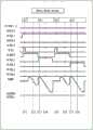
图11是图示了针对像素部120的单位像素行进行的反馈阶段处理的流程的示例的时序图。FIG. 11 is a timing chart illustrating an example of the flow of feedback stage processing performed for the unit pixel row of the
在这种情况下,如图11所示,使选择控制信号(ΦSEL1)导通(步骤S121)且使复位控制信号(ΦRST1)导通(步骤S122)。In this case, as shown in FIG. 11, the selection control signal (ΦSEL1) is turned on (step S121) and the reset control signal (ΦRST1) is turned on (step S122).
其后,在时刻T1进行自动归零处理(AZ)(步骤S123)。此时,AZ连接控制信号(ΦAZ)和VRST连接控制信号(ΦVRST)是导通的。After that, the auto-zero processing (AZ) is performed at time T1 (step S123). At this time, the AZ connection control signal (ΦAZ) and the VRST connection control signal (ΦVRST) are turned on.
据此,如图12所示,比较部171的输入端和输出端是短路的且电源电势VRST施加在垂直信号线(VSL)的VSL开关161与电容器182之间。Accordingly, as shown in FIG. 12 , the input terminal and the output terminal of the
在时刻T2,进行针对单位像素121-11的处理(步骤S124至S126)。此时,FBEN连接控制信号(ΦFBEN)是导通的,且此外,与单位像素121-11相对应的VSL连接控制信号(ΦVSL1)和FBL连接控制信号(ΦFBL1)是导通的。At time T2, processing for the unit pixel 121-11 is performed (steps S124 to S126). At this time, the FBEN connection control signal (ΦFBEN) is turned on, and further, the VSL connection control signal (ΦVSL1) and the FBL connection control signal (ΦFBL1) corresponding to the unit pixels 121-11 are turned on.
据此,如图13所示,比较部171的输出作为复位电平被反馈至单位像素121-11的浮动扩散部(FD)。此外,该复位电平被读取以供给至比较部171的VSL侧输入端子。Accordingly, as shown in FIG. 13 , the output of the
此时,从单位像素121-11读取的信号的信号电平可以被表示为VRST+ΔVOUT*GSF。此外,比较部171的输出(比较结果)的信号电平VOUT可以由下面的方程式(1)来表示。At this time, the signal level of the signal read from the unit pixel 121-11 can be expressed as VRST+ΔVOUT*GSF . Further, the signal level VOUT of the output (comparison result) of the
VOUT=VRST+Vgs(amp)+ΔVOUT…(1)VOUT=VRST+Vgs(amp)+ΔVOUT…(1)
表示比较部171的输出(比较结果)的信号电平VOUT的误差的ΔVOUT可以通过下面的方程式(2)来获得。ΔVOUT representing the error of the signal level VOUT of the output (comparison result) of the
ΔVOUT=ΔVth/(1+GSF×GCM)…(2)ΔVOUT=ΔVth/(1+GSF ×GCM )…(2)
例如,当放大晶体管134的阈值电压Vth的误差ΔVth是100[mV]、GCM是30且GSF是0.85时,ΔVOUT是3.8[mV]。For example, when the error ΔVth of the threshold voltage Vth of the amplifying
其后,使FBEN连接控制信号(ΦFBEN)、VSL连接控制信号(ΦVSL1)和FBL连接控制信号(ΦFBL1)截止。特别地,通过截止FBL连接控制信号(ΦFBL1),如图14所示,在单位像素121-11的浮动扩散部(FD)和从浮动扩散部(FD)到FBL开关162-1的反馈线(FBL1)中,电势[VOUT+ΔVnoise(FBL1)]被保持为复位电平。ΔVnoise(FBL1)包括FBL开关162-1的馈通和kTC噪声。以下,当不需要区别说明各FBL开关162(反馈线(FBL))时,将它们称为ΔVnoise(FBL)。换言之,ΔVnoise(FBLn)是与第n条反馈线(FBLn)相对应的电势,并且包括FBL开关162-n的馈通和kTC噪声。此外,使用ΔVnoise(FBL)进行的说明可以应用于任何ΔVnoise(FBLn)。After that, the FBEN connection control signal (ΦFBEN), the VSL connection control signal (ΦVSL1 ), and the FBL connection control signal (ΦFBL1 ) are turned off. Specifically, by turning off the FBL connection control signal (ΦFBL1), as shown in FIG. 14, at the floating diffusion (FD) of the unit pixel 121-11 and the feedback line (FD) from the floating diffusion (FD) to the FBL switch 162-1 In FBL1), the potential [VOUT+ΔVnoise(FBL1)] is held at the reset level. ΔVnoise(FBL1) includes the feedthrough and kTC noise of FBL switch 162-1. Hereinafter, when each FBL switch 162 (feedback line (FBL)) does not need to be described separately, they will be referred to as ΔVnoise (FBL). In other words, ΔVnoise(FBLn) is the potential corresponding to the nth feedback line (FBLn) and includes the feedthrough and kTC noise of the FBL switch 162-n. Furthermore, the description using ΔVnoise(FBL) can be applied to any ΔVnoise(FBLn).
接着,针对单位像素121-21,重复类似处理。即,与在时刻T1一样,在时刻T3首先进行自动归零处理(AZ)。Next, similar processing is repeated for the unit pixels 121-21. That is, the auto-zero processing (AZ) is first performed at time T3 as at time T1.
据此,如图14所示,比较部171的输入端和输出端是短路的且电源电势VRST施加在垂直信号线(VSL)的VSL开关161与电容器182之间。Accordingly, as shown in FIG. 14 , the input terminal and the output terminal of the
接着,在时刻T4,进行针对单位像素121-21的处理(步骤S124至S126)。此时,FBEN连接控制信号(ΦFBEN)是导通的,且此外,与单位像素121-21相对应的VSL连接控制信号(ΦVSL2)和FBL连接控制信号(ΦFBL2)是导通的。Next, at time T4, processing for the unit pixels 121-21 is performed (steps S124 to S126). At this time, the FBEN connection control signal (ΦFBEN) is turned on, and further, the VSL connection control signal (ΦVSL2) and the FBL connection control signal (ΦFBL2) corresponding to the unit pixels 121-21 are turned on.
据此,如图15所示,比较部171的输出作为复位电平被反馈至单位像素121-21的浮动扩散部(FD)。此外,复位电平被读取以供给至比较部171的VSL侧输入端子。Accordingly, as shown in FIG. 15 , the output of the
此外,从时刻T5至时刻T8,分别针对单位像素121-31和121-41,重复类似处理。图16图示了在时刻T8的状态。此时,比较部171的输出VOUT(即,电势[VRST+Vgs(amp)+ΔVOUT])被反馈至单位像素121-41的浮动扩散部(FD)。同时,在单位像素121-11至121-31的各者中,在浮动扩散部(FD)和从浮动扩散部(FD)至FBL开关162的反馈线(FBL)中,电势[VOUT+ΔVnoise(FBL)]被保持为复位电平。如上所述,ΔVnoise(FBL)的值包括FBL开关162的馈通和kTC噪声,使得对于各单位像素121(反馈线(FBL))而言是独立的。即,在各单位像素121(反馈线(FBL))中保持有以与单位像素(反馈线(FBL))相对应的FBL开关162为依据的值的电势[VOUT+ΔVnoise(FBL)]。Further, from time T5 to time T8, similar processing is repeated for the unit pixels 121-31 and 121-41, respectively. FIG. 16 illustrates the state at time T8. At this time, the output VOUT of the comparison part 171 (ie, the potential [VRST+Vgs(amp)+ΔVOUT]) is fed back to the floating diffusion (FD) of the unit pixel 121 - 41 . Meanwhile, in each of the unit pixels 121-11 to 121-31, in the floating diffusion (FD) and the feedback line (FBL) from the floating diffusion (FD) to the FBL switch 162, the potential [VOUT+ΔVnoise( FBL)] is held at the reset level. As described above, the value of ΔVnoise(FBL) includes the feedthrough of the FBL switch 162 and the kTC noise so as to be independent for each unit pixel 121 (feedback line (FBL)). That is, the potential [VOUT+ΔVnoise(FBL)] based on the value of the FBL switch 162 corresponding to the unit pixel (feedback line (FBL)) is held in each unit pixel 121 (feedback line (FBL)).
此后,针对单位像素121-41,通过截止FBL连接控制信号(ΦFBL1)(通过断开FBL开关162-4),在浮动扩散部(FD)和从浮动扩散部(FD)到FBL开关162-4的反馈线(FBL4)中,也保持有电势[VOUT+ΔVnoise(FBL4)]作为复位电平。Thereafter, for the unit pixel 121-41, by turning off the FBL connection control signal (ΦFBL1) (by turning off the FBL switch 162-4), at the floating diffusion (FD) and from the floating diffusion (FD) to the FBL switch 162-4 In the feedback line (FBL4) of , the potential [VOUT+ΔVnoise(FBL4)] is also held as a reset level.
以这样的方式,在单位像素121-11至121-41的各者中,在浮动扩散部(FD)和从浮动扩散部(FD)至FBL开关162的反馈线(FBL)中,电势[VOUT+ΔVnoise(FBL)]被保持为复位电平。In this way, in each of the unit pixels 121-11 to 121-41, in the floating diffusion (FD) and the feedback line (FBL) from the floating diffusion (FD) to the FBL switch 162, the potential [VOUT +ΔVnoise(FBL)] is held at the reset level.
如上所述,当将比较部171的输出反馈至当前行的所有单位像素121时,使复位控制信号(ΦRST1)截止(时刻T9,步骤S129)。据此,单位像素121-11至121-41的各者的浮动扩散部(FD)被复位。As described above, when the output of the
由此,如图17所示,各单位像素121的复位晶体管133被截止,且在单位像素121-11至121-41各者的浮动扩散部(FD)中,电势[VOUT+ΔVnoise(FBL)+ΔVnoise(RST)]得到保持。ΔVnoise(RST)包括复位晶体管133的馈通和kTC噪声。因此,ΔVnoise(RST)的值对于各单位像素121(反馈线(FBL))而言也是独立的。即,在各单位像素121的浮动扩散部(FD)中,以取决于与单位像素(反馈线(FBL))相对应的FBL开关162和复位晶体管133的值的电势[VOUT+ΔVnoise(FBL)+ΔVnoise(RST)]得到保持。据此,各单位像素121的放大晶体管134的阈值电压Vth的变化减小。Thereby, as shown in FIG. 17 , the
图18是图示了针对像素部120下的单位像素行进行的反馈阶段处理的流程的示例的时序图。FIG. 18 is a timing chart illustrating an example of the flow of feedback stage processing performed for the unit pixel row under the
在这种情况下,如图18所示,使选择控制信号(SEL2)导通(步骤S121)且使复位控制信号(RST2)导通(步骤S122)。即,将要处理单位像素121-12至121-42的单位像素行。在这种情况下,与参照图11说明的情况一样,进行自动归零处理和针对各单位像素121的处理。In this case, as shown in FIG. 18, the selection control signal (SEL2) is turned on (step S121) and the reset control signal (RST2) is turned on (step S122). That is, the unit pixel rows of the unit pixels 121-12 to 121-42 are to be processed. In this case, as in the case described with reference to FIG. 11 , the auto-zero processing and the processing for each
如图19所示,当在时刻T11进行自动归零处理时,在先前处理过的单位像素121-11至121-41的各者的浮动扩散部(FD)中,电势[VOUT+ΔVnoise(FBL)+ΔVnoise(RST)]得到保持。As shown in FIG. 19, when the auto-zero processing is performed at time T11, in the floating diffusion (FD) of each of the previously processed unit pixels 121-11 to 121-41, the potential [VOUT+ΔVnoise(FBL) )+ΔVnoise(RST)] is maintained.
然后,当进行从时刻T11至时刻T18的处理时,如图20所示,在单位像素121-12至121-42的各者的浮动扩散部(FD)和从浮动扩散部(FD)到FBL开关162的反馈线(FBL)中,电势[VOUT+ΔVnoise(FBL)]被保持为复位电平。Then, when the processing from time T11 to time T18 is performed, as shown in FIG. 20 , at the floating diffusion (FD) of each of the unit pixels 121 - 12 to 121 - 42 and from the floating diffusion (FD) to FBL In the feedback line (FBL) of the switch 162, the potential [VOUT+ΔVnoise(FBL)] is held at the reset level.
如上所述,当比较部171的输出被反馈至当前行的所有单位像素121时,使复位控制信号(ΦRST2)截止(时刻T19,步骤S129)。据此,单位像素121-12至121-42的各者的浮动扩散部(FD)被复位。As described above, when the output of the
由此,如图21所示,各单位像素121的复位晶体管被截止,且在单位像素121-12至121-42的各者的浮动扩散部(FD)中,电势[VOUT+ΔVnoise(FBL)+ΔVnoise(RST)]得到保持。由此,各单位像素121的放大晶体管的阈值电压Vth的变化减小。Thereby, as shown in FIG. 21, the reset transistor of each
因此,图像传感器100可以抑制各像素的放大晶体管134的阈值电压Vth的变化。据此,图像传感器100可以抑制被摄图像的图像质量下降。即,本发明也可以被应用于含有区域A/D转换器的图像传感器。Therefore, the
此外,FBL开关162的设置使得可以不必配备与像素列一样多的复位控制线(RST),以使能够自由设置针对一个放大器(比较部171)的将被反馈的像素列的数量。即,配线的数量变得明显少了,使得可以增大配线层布局的自由度。Furthermore, the setting of the FBL switch 162 makes it unnecessary to provide as many reset control lines (RSTs) as pixel columns, so that the number of pixel columns to be fed back for one amplifier (comparison section 171 ) can be freely set. That is, the number of wirings becomes remarkably small, making it possible to increase the degree of freedom in the layout of wiring layers.
此外,可以通过如上所述地设置FBL开关162且如上所述地驱动它来实现本发明,使得可以抑制电路规模的增加。此外,如图7所示,FBL开关162可以布置在像素区域(像素阵列101)以外。因此,可以在不改变像素内的晶体管数量的情况下实现本发明。因此,可以更加容易地应用本发明且可以抑制成本增加。Furthermore, the present invention can be realized by setting the FBL switch 162 as described above and driving it as described above, so that an increase in circuit scale can be suppressed. Furthermore, as shown in FIG. 7, the FBL switch 162 may be arranged outside the pixel area (pixel array 101). Therefore, the present invention can be implemented without changing the number of transistors within a pixel. Therefore, the present invention can be applied more easily and cost increase can be suppressed.
此外,本发明的应用抑制了各垂直信号线(VSL)的电势的变化,使得可以使作为电流源的负载MOS的D范围更窄。Furthermore, the application of the present invention suppresses the variation of the potential of each vertical signal line (VSL), so that the D range of the load MOS as the current source can be made narrower.
<预设读取阶段处理的流程><Flow of Preset Read Phase Processing>
接着,参照图22的流程图来说明在图8的步骤S103中执行的预设读取阶段处理的流程的示例。Next, an example of the flow of the preset read phase processing executed in step S103 of FIG. 8 will be described with reference to the flowchart of FIG. 22 .
当预设读取阶段处理开始时,在步骤S151中,控制部110控制区域扫描部111,并且将当前像素部120的还未被处理的单位像素行(单位像素121的行)选择作为待被处理的目标。例如,区域扫描部111使还未被处理的各单位像素行中的任一行的选择控制信号(SEL)导通。When the preset reading stage process starts, in step S151, the control section 110 controls the area scanning section 111, and selects the unit pixel row (row of the unit pixel 121) of the
在步骤S152中,控制部110控制A/D转换控制部113等以执行自动归零处理(AZ)。例如,A/D转换控制部113使与当前像素部120相对应的区域A/D转换器143所用的AZ连接控制信号(AZ)导通。此外,A/D转换控制部113使区域A/D转换器143的VRST连接控制信号(VRST)导通。In step S152, the control section 110 controls the A/D
在步骤S153中,控制部110控制A/D转换控制部113以读取kTC噪声。例如,A/D转换控制部113在VRST连接控制信号(VRST)保持导通的情况下将D/A转换器(DAC)144产生的斜坡波(RAMP)输入到比较部171的DAC侧输入端子,并且将斜坡波(RAMP)与电源电势VRST进行比较。In step S153, the control section 110 controls the A/D
当比较结束时,在步骤S154中,控制部110控制VSL连接控制部112以将还未被处理的单位像素列(单位像素121的列)选择作为待被处理的目标。例如,VSL连接控制部112使当前像素部120的任一个VSL连接控制信号(VSL)导通。据此,将当前单位像素行中的一个单位像素121选择作为待被处理的目标。When the comparison ends, in step S154 , the control section 110 controls the VSL
在步骤S155中,控制部110控制VSL连接控制部112和A/D转换控制部113以从当前单位像素121读取复位电平。例如,A/D转换控制部113将D/A转换器(DAC)144产生的斜坡波(RAMP)作为参考电压输入到比较部171的DAC侧输入端子,并且将从当前单位像素121读取的复位电平与参考电压(斜坡波(RAMP))进行比较。In step S155 , the control section 110 controls the VSL
当比较结束时,在步骤S156中,控制部110判断当前像素部120的当前单位像素行的所有单位像素列是否都得到处理。当判定存在还未被处理的单位像素列时,程序返回到步骤S152且重复后续的处理。此外,在步骤S156中,当判定当前单位像素行的所有单位像素列都得到处理时,程序转到步骤S157。When the comparison ends, in step S156 , the control section 110 determines whether all the unit pixel columns of the current unit pixel row of the
在步骤S157中,控制部110控制区域扫描部111以取消选择在步骤S151中选择的当前行。例如,区域扫描部111使步骤S151中导通的选择控制信号(SEL)截止。In step S157, the control section 110 controls the area scanning section 111 to deselect the current row selected in step S151. For example, the area scanning unit 111 turns off the selection control signal (SEL) that was turned on in step S151.
在步骤S158中,控制部110判断当前像素部120的所有单位像素行是否都得到处理。当判定存在还未被处理的单位像素行时,程序返回到步骤S151且重复后续的处理。此外,在步骤S158中,当判定当前像素部120的所有单位像素行(即,当前像素部120的所有单位像素121)都得到处理时,预设读取阶段处理结束且程序返回到图8。In step S158, the control unit 110 determines whether all the unit pixel rows of the
即,针对当前像素部120的各单位像素行,进行步骤S151至S158的处理。当处理过所有单位像素行时,程序转到下一个阶段(电荷传输)。That is, the processing of steps S151 to S158 is performed for each unit pixel row of the
<预设读取阶段的时序图><Timing Diagram of Preset Read Phase>
图23是针对像素部120的单位像素121-11和121-21进行的预设读取阶段处理的流程的示例的时序图。FIG. 23 is a timing chart of an example of the flow of the preset read phase processing performed for the unit pixels 121 - 11 and 121 - 21 of the
在这种情况下,如图23所示,使选择控制信号(ΦSEL1)导通(步骤S151)。In this case, as shown in FIG. 23, the selection control signal (ΦSEL1) is turned on (step S151).
其后,在时刻T21进行自动归零处理(AZ)(步骤S152)。此时,AZ连接控制信号(ΦAZ)和VRST连接控制信号(ΦVRST)是导通的。After that, the auto-zero processing (AZ) is performed at time T21 (step S152). At this time, the AZ connection control signal (ΦAZ) and the VRST connection control signal (ΦVRST) are turned on.
据此,如图24所示,比较部171的输入端和输出端是短路的且电源电势VRST施加在垂直信号线(VSL)的VSL开关161与电容器182之间(即,施加于比较部171的VSL侧输入端子)。Accordingly, as shown in FIG. 24 , the input terminal and the output terminal of the
在时刻T22,读取kTC噪声(步骤S153)。此时,在VRST连接控制信号(ΦVRST)保持导通的情况下(即,如图25所示,在电源电势VRST施加于比较部171的VSL侧输入端子的情况下),D/A转换器(DAC)144供给来的斜坡波(参考电压)输入到比较部171的DAC侧输入端子。即,电源电势VRST与参考电势(斜坡波)进行比较。据此,读取kTC噪声(ΔVnoise(CM))。At time T22, kTC noise is read (step S153). At this time, in the case where the VRST connection control signal (ΦVRST) is kept on (ie, in the case where the power supply potential VRST is applied to the VSL side input terminal of the
接着,在时刻T23选择当前单位像素列(步骤S154)。此时,VRST连接控制信号(ΦVRST)是截止的且与当前单位像素121-11相对应的VSL连接控制信号(ΦVSL1)是导通的。即,如图26所示,保持在单位像素121-11的浮动扩散部(FD)中的复位电平传输到比较部171的VSL侧输入端子。因此,比较部171的VSL侧输入端子处的电压变为[ΔVnoise(CM)+[ΔVOUT+ΔVnoise(FBL)+ΔVnoise(RST)]*GSF]。同时,尽管因电容器182介入而乘以电容比,但是电容比充分接近于“1”以致可以被省略。Next, the current unit pixel row is selected at time T23 (step S154). At this time, the VRST connection control signal (ΦVRST) is turned off and the VSL connection control signal (ΦVSL1 ) corresponding to the current unit pixel 121 - 11 is turned on. That is, as shown in FIG. 26 , the reset level held in the floating diffusion (FD) of the unit pixel 121 - 11 is transferred to the VSL side input terminal of the
在时刻T24,从当前单位像素读取复位电平(步骤S155)。即,如图27所示,D/A转换器(DAC)144供给来的斜坡波(参考电压)被输入至比较部171的DAC侧输入端子,且单位像素121-11的复位电平与参考电势(斜坡波)进行比较。At time T24, the reset level is read from the current unit pixel (step S155). That is, as shown in FIG. 27 , the ramp wave (reference voltage) supplied from the D/A converter (DAC) 144 is input to the DAC side input terminal of the
此时,比较部171的VSL侧输入端子处的电压变为[ΔVnoise(CM)+[ΔVOUT+ΔVnoise(FBL)+ΔVnoise(RST)]*GSF]。因此,从单位像素121-11读取的信号的信号电平(Signal(P))由下面的方程式(3)来表示。At this time, the voltage at the VSL side input terminal of the
Signal(P)=[ΔVnoise(CM)+[ΔVOUT+ΔVnoise(FBL)+ΔVnoise(RST)]*GSF]-[ΔVnoise(CM)]Signal(P)=[ΔVnoise(CM)+[ΔVOUT+ΔVnoise(FBL)+ΔVnoise(RST)]*GSF ]-[ΔVnoise(CM)]
=[ΔVOUT+ΔVnoise(FBL)+ΔVnoise(RST)]*GSF…(3)=[ΔVOUT+ΔVnoise(FBL)+ΔVnoise(RST)]*GSF …(3)
接着,从时刻T25至时刻T28,针对单位像素121-21,重复类似处理。例如,在时刻T27,如图28所示,VSL连接控制信号(ΦVSL2)是导通的且保持在单位像素121-21的浮动扩散部(FD)中的复位电平被传输至比较部171的VSL侧输入端子。Next, from time T25 to time T28, similar processing is repeated for the unit pixels 121-21. For example, at time T27, as shown in FIG. 28, the VSL connection control signal (ΦVSL2) is on and the reset level held in the floating diffusions (FD) of the unit pixels 121-21 is transferred to the
然后,在时刻T28,如图29所示,D/A转换器(DAC)144供给来的斜坡波(参考电压)被输入至比较部171的DAC侧输入端子且单位像素121-21的复位电平与参考电势(斜坡波)进行比较。Then, at time T28, as shown in FIG. 29, the ramp wave (reference voltage) supplied from the D/A converter (DAC) 144 is input to the DAC side input terminal of the
图30是图示了针对像素部120的单位像素121-31和121-41进行的预设读取阶段处理的流程的示例的时序图。如图30所示,针对单位像素121-31和121-41的各者,重复与针对单位像素121-11进行的处理类似的处理。FIG. 30 is a timing chart illustrating an example of the flow of preset read phase processing performed for the unit pixels 121 - 31 and 121 - 41 of the
图31是图示了针对像素部120的单位像素121-12和121-22进行的预设读取阶段处理的流程的示例的时序图。如图31所示,针对单位像素121-12和121-22的各者,重复与针对单位像素121-11进行的处理类似的处理。然而,在这种情况下,使选择控制信号(ΦSEL2)导通(步骤S151)。FIG. 31 is a timing chart illustrating an example of the flow of preset read phase processing performed for the unit pixels 121 - 12 and 121 - 22 of the
图32是图示了针对像素部120的单位像素121-32和121-42进行的预设读取阶段处理的流程的示例的时序图。如图32所示,针对单位像素121-32和121-42的各者,重复与针对单位像素121-12进行的处理类似的处理。FIG. 32 is a timing chart illustrating an example of the flow of preset read phase processing performed for the unit pixels 121 - 32 and 121 - 42 of the
<电荷传输><Charge transfer>
图33是图示了在图8的步骤S104中进行的电荷传输的状态的示例的时序图。FIG. 33 is a timing chart illustrating an example of the state of charge transfer performed in step S104 of FIG. 8 .
如图33所示,在时刻T61,区域扫描部111使当前像素部120的单位像素行的传输控制信号(ΦTRG1和2)导通且使其它控制信号截止。据此,如图34所示,累积于光电二极管(PD)131中的电荷被传输至当前像素部120的所有单位像素121中的浮动扩散部(FD)。As shown in FIG. 33 , at time T61 , the area scanning unit 111 turns on the transfer control signals ( ΦTRG1 and 2 ) of the unit pixel row of the
<数据读取阶段处理的流程><Flow of data read phase processing>
接着,参照图35的流程图来说明在图8的步骤S105中执行的数据读取阶段处理的流程的示例。Next, an example of the flow of the data read phase processing executed in step S105 of FIG. 8 will be described with reference to the flowchart of FIG. 35 .
如图35所示,控制部110执行与预设读取阶段处理(图22)的处理(步骤S151至S158)一样的数据读取阶段处理的处理(步骤S171至S178)。As shown in FIG. 35 , the control section 110 executes processing (steps S171 to S178 ) similar to the processing (steps S151 to S158 ) of the preset reading phase processing ( FIG. 22 ).
然而,在步骤S175中,控制部110从当前单位像素121不是读取复位电平而是读取与通过图8的步骤S104中的处理从光电二极管(PD)131传输到浮动扩散部(FD)的电荷相对应的像素信号,并且将该像素信号与参考电压(斜坡波)进行比较。However, in step S175 , the control section 110 does not read the reset level from the
<数据读取阶段的时序图><Timing diagram of data read phase>
图36是图示了针对像素部120的单位像素121-11和121-21进行的数据读取阶段处理的流程的示例的时序图。FIG. 36 is a timing chart illustrating an example of the flow of the data read phase processing performed for the unit pixels 121 - 11 and 121 - 21 of the
如图36所示,在这种情况下,与图23所示的预设读取阶段处理的情况一样,执行各处理。As shown in FIG. 36 , in this case, as in the case of the preset read stage process shown in FIG. 23 , each process is executed.
例如,使选择控制信号(ΦSEL1)导通(步骤S171),且在时刻T71进行自动归零处理(AZ)(步骤S172)。此时,AZ连接控制信号(ΦAZ)和VRST连接控制信号(ΦVRST)是导通的。For example, the selection control signal (ΦSEL1) is turned on (step S171), and the auto-zero processing (AZ) is performed at time T71 (step S172). At this time, the AZ connection control signal (ΦAZ) and the VRST connection control signal (ΦVRST) are turned on.
然后,例如,在时刻T72,如图37所示地读取kTC噪声(步骤S173)。即,将电源电势VRST与参考电势(斜坡波)进行比较。据此,读取kTC噪声(ΔVnoise’(CM))。Then, for example, at time T72, kTC noise is read as shown in FIG. 37 (step S173). That is, the power supply potential VRST is compared with the reference potential (ramp wave). Accordingly, the kTC noise (ΔVnoise'(CM)) is read.
此外,例如,在时刻T73选择当前单位像素列(步骤S174)。此时,VRST连接控制信号(ΦVRST)是截止的且与当前单位像素121-11相对应的VSL连接控制信号(ΦVSL1)是导通的。即,如图38所示,与保持在单位像素121-11的浮动扩散部(FD)中的电荷相对应的像素信号被传输至比较部171的VSL侧输入端子。因此,比较部171的VSL侧输入端子处的电压变为[Vsig+ΔVnoise'(CM)+[ΔVOUT+ΔVnoise(FBL)+ΔVnoise(RST)]*GSF]。Further, for example, the current unit pixel row is selected at time T73 (step S174). At this time, the VRST connection control signal (ΦVRST) is turned off and the VSL connection control signal (ΦVSL1 ) corresponding to the current unit pixel 121 - 11 is turned on. That is, as shown in FIG. 38 , the pixel signal corresponding to the charge held in the floating diffusion (FD) of the unit pixel 121 - 11 is transferred to the VSL side input terminal of the
在时刻T74,从当前单位像素读取复位电平(步骤S175)。即,如图39所示,将D/A转换器(DAC)144供给来的斜坡波(参考电压)输入到比较部171的DAC侧输入端子,并且将单位像素121-11的像素信号的信号电平与参考电势(斜坡波)进行比较。At time T74, the reset level is read from the current unit pixel (step S175). That is, as shown in FIG. 39 , the ramp wave (reference voltage) supplied from the D/A converter (DAC) 144 is input to the DAC side input terminal of the
此时,比较部171的VSL侧输入端子处的电压变为[Vsig+ΔVnoise'(CM)+[ΔVOUT+ΔVnoise(FBL)+ΔVnoise(RST)]*GSF]。因此,从单位像素121-11读取的像素信号的信号电平(Signal(D))由下面的方程式(4)来表示。At this time, the voltage at the VSL side input terminal of the
Signal(D)=[Vsig+ΔVnoise'(CM)+[ΔVOUT+ΔVnoise(FBL)+ΔVnoise(RST)]*GSF]-[ΔVnoise'(CM)]Signal(D)=[Vsig+ΔVnoise'(CM)+[ΔVOUT+ΔVnoise(FBL)+ΔVnoise(RST)]*GSF ]-[ΔVnoise'(CM)]
=Vsig+[ΔVOUT+ΔVnoise(FBL)+ΔVnoise(RST)]*GSF…(4)=Vsig+[ΔVOUT+ΔVnoise(FBL)+ΔVnoise(RST)]*GSF …(4)
从时刻T75至时刻T78,针对单位像素121-21,重复类似处理。From time T75 to time T78, similar processing is repeated for the unit pixels 121-21.
图40是图示了针对像素部120的单位像素121-31和121-41进行的数据读取阶段处理的流程的示例的时序图。如图40所示,针对单位像素121-31和121-41的各者,重复与针对单位像素121-11进行的处理类似的处理。FIG. 40 is a timing chart illustrating an example of the flow of the data read phase processing performed for the unit pixels 121 - 31 and 121 - 41 of the
图41是图示了针对像素部120的单位像素121-12和121-22进行的数据读取阶段处理的流程的示例的时序图。如图41所示,针对单位像素121-12和121-22的各者,重复与针对单位像素121-11进行的处理类似的处理。然而,在这种情况下,使选择控制信号(ΦSEL2)导通(步骤S171)。FIG. 41 is a timing chart illustrating an example of the flow of the data reading phase processing performed for the unit pixels 121 - 12 and 121 - 22 of the
图42是图示了针对像素部120的单位像素121-32和121-42进行的数据读取阶段处理的流程的示例的时序图。如图42所示,针对单位像素121-32和121-42的各者,重复与针对单位像素121-12进行的处理类似的处理。FIG. 42 is a timing chart illustrating an example of the flow of the data read phase processing performed for the unit pixels 121 - 32 and 121 - 42 of the
通过进行如上所述的各处理,图像传感器100可以抑制被摄图像的图像质量下降。By performing each process as described above, the
<2.第二实施例><2. Second Embodiment>
<成像装置><Imaging device>
同时,本发明可应用于图像传感器件以外的器件。例如,本发明也可以应用于例如成像装置等具有图像传感器件的装置(电子设备等)。图43是图示了作为应用本发明的电子设备的示例的成像装置的主要构造例的框图。图43所示的成像装置600是拍摄被摄体的图像且将被摄体的图像作为电信号输出的装置。Meanwhile, the present invention can be applied to devices other than image sensing devices. For example, the present invention can also be applied to an apparatus (electronic equipment, etc.) having an image sensing device such as an imaging apparatus. 43 is a block diagram illustrating a main configuration example of an imaging apparatus as an example of an electronic apparatus to which the present invention is applied. The
如图43所示,成像装置600包括光学部611、CMOS图像传感器612、图像处理器613、显示部614、编码解码处理器615、存储部616、输出部617、通信部618、控制部621、操作部622和驱动器623。As shown in FIG. 43 , the
光学部611由调整用于被摄体的焦点且聚集来自焦点位置的光的透镜、调整曝光的光圈和控制成像时间的快门等形成。光学部611使来自被摄体的光(入射光)透过以使之供给到CMOS图像传感器612。The
CMOS图像传感器612进行入射光的光电转换且进行各像素的信号(像素信号)的A/D转换,进行例如CDS等信号处理,并且将处理后的被摄图像数据供给到图像处理器613。The
图像处理器613对通过图像传感器612而获得的被摄图像数据进行图像处理。更加具体地,图像处理器613对CMOS图像传感器612供给来的被摄图像数据进行例如混色校正、黑电平校正、白平衡校正、去马赛克处理、矩阵处理、伽马校正和YC转换等各种类型的图像处理。图像处理器613将经过图像处理的被摄图像数据供给到显示部614。The
显示部614(例如,被形成为液晶显示器等)显示图像处理器613供给来的被摄图像数据的图像(例如,被摄体的图像)。The display unit 614 (formed as a liquid crystal display or the like, for example) displays an image of the captured image data (eg, an image of a subject) supplied from the
根据需要,图像处理器613还将经过图像处理的被摄图像数据供给到编码解码处理器615。The
编码解码处理器615将预定系统的编码处理施加于图像处理器613供给来的被摄图像数据,并且将获得的编码数据供给到存储部616。此外,编码解码处理器615读取记录于存储部616中的编码数据,解码该编码数据以产生解码图像数据且将解码图像数据供给到图像处理器613。The
图像处理器613将预定的图像处理施加于编码解码处理器615供给来的解码图像数据。图像处理器613将经过图像处理的解码图像数据供给到显示部614。显示部614(例如,被形成为液晶显示器等)显示图像处理器613供给来的解码图像数据的图像。The
此外,编码解码处理器615可以将通过对图像处理器613供给来的被摄图像数据进行编码而获得的编码数据或从存储部616读取的被摄图像数据的编码数据供给到输出部617,并且可以将这些数据输出到成像装置600的外部。此外,编码解码处理器615可以将编码前的被摄图像数据或通过对从存储部616读取的编码数据进行解码而获得的解码图像数据供给到输出部617,并且可以将这些数据输出到成像装置600的外部。In addition, the
此外,编码解码处理器615也可以通过通信部618将被摄图像数据、被摄图像数据的编码数据或解码图像数据传输到另一个装置。编码解码处理器615也可以通过通信部618获得被摄图像数据和图像数据的编码数据。编码解码处理器615适当地编码或解码通过通信部618而获得的被摄图像数据和图像数据的编码数据。编码解码处理器615可以将获得的图像数据或编码数据供给到图像处理器613或可以将这些数据输出到如上所述的存储部616、输出部617和通信部618。Also, the
存储部616存储编码解码处理器615供给来的编码数据等。根据需要,编码解码处理器615读取存储于存储部616的编码数据以将它们解码。将通过解码处理而获得的被摄图像数据供给到显示部614,并且显示与被摄图像数据相对应的被摄图像。The
输出部617(其包括例如外部输出端子等外部输出接口)通过外部输出接口将通过编码解码处理器615而供给来的各种数据输出到成像装置600的外部。The output section 617 (which includes an external output interface such as an external output terminal) outputs various data supplied by the
通信部618将编码解码处理器615供给来的例如图像数据和编码数据等各种类型的信息供给到作为预定通信(有线或无线通信)的通信配对装置的另一个装置。通信部618也获得来自作为预定通信(有线或无线通信)的通信配对装置的另一个装置的例如图像数据和编码数据等各种类型的信息,并且将这些信息供给到编码解码处理器615。The
控制部621控制成像装置600的各处理器(操作部622、驱动器623和由虚线620围绕的各处理器)的操作。The
操作部622(其例如由jog dial(商标)、按键、按钮或触摸面板等任意输入器件形成)接收例如用户等输入的操作,并且将与操作输入相对应的信号供给到控制部621。The operation section 622 (which is formed of, for example, any input device such as jog dial (trademark), keys, buttons, or touch panel) receives operations such as user input, and supplies a signal corresponding to the operation input to the
驱动器623例如读取其上安装的例如磁盘、光盘、磁光盘和半导体存储器等可移除媒介624。驱动器623从可移除媒介624读取例如程序和数据等各种类型的信息,并且将这些信息供给到控制部621。此外,当可写入的可移除媒介624安装在驱动器623上时,驱动器623例如将通过控制部621而供给来的例如图像数据和编码数据等各种类型的信息存储到可移除媒介624。The
作为上述的成像装置600的CMOS图像传感器612,能够应用上面各实施例所述的本发明。即,上述的图像传感器100用作CMOS图像传感器612。据此,CMOS图像传感器612可以抑制被摄图像的图像质量下降。因此,成像装置600可以通过摄取被摄体的图像来获得更高质量的被摄图像。As the
可以由硬件或软件执行上述系列的处理。当由软件执行上述系列的处理时,从网络或记录媒介安装形成软件的程序。The above-described series of processes can be executed by hardware or software. When the above-described series of processes are executed by software, a program forming the software is installed from a network or a recording medium.
记录媒介例如由图43所示的记录有程序的并且被分配用于将程序传递给用户的可移除媒介624以与装置主体分离的形式形成。可移除媒介624包括磁盘(其包括软盘)和光盘(其包括CD-ROM和DVD)。还包括磁光盘(其包括MD(Mini Disc:微型盘))和半导体存储器。The recording medium is formed, for example, by a
在这种情况下,可以通过将可移除媒介624安装在驱动器623上来将程序安装在存储部616上。In this case, the program can be installed on the
也可以通过例如局域网、因特网和数字卫星广播等有线或无线传输媒介来提供程序。在这种情况下,可以通过通信部618接收程序以将程序安装在存储部616上。The programs may also be provided through wired or wireless transmission media such as local area networks, the Internet, and digital satellite broadcasting. In this case, the program can be received through the
也可以事先将程序安装在存储部616上和控制部621内的ROM(Read Only Memory:只读存储器)上。The program may be installed in the
同时,计算机执行的程序可以是按照本说明书所述的顺序以时间顺序进行其处理的程序或可以是并行地或必要时(例如,当发起调用时)进行其处理的程序。Meanwhile, the program executed by the computer may be a program whose processing is performed chronologically in the order described in this specification or may be a program whose processing is performed in parallel or when necessary (eg, when a call is made).
此外,在本说明书中,记录于记录媒介的程序的说明步骤不仅包括按照所述的顺序以时间顺序进行的处理而且包括未必以时间顺序进行的并行地或单独地执行的处理。In addition, in this specification, the description steps of the program recorded in the recording medium include not only processing performed in time series in the stated order but also processing performed in parallel or individually which are not necessarily performed in time series.
此外,上述各步骤中的处理可以在上述的各装置中或在上述装置以外的任何装置中得到执行。在这种情况下,执行处理的装置可以包括用于执行处理所需的功能(功能模块等)。此外,处理所需的信息可以被适当地传输到装置。In addition, the processing in each of the above-described steps may be performed in each of the above-described devices or in any device other than the above-described devices. In this case, the means for executing the processing may include functions (functional modules, etc.) required for executing the processing. Furthermore, information required for processing can be appropriately transmitted to the device.
此外,在本说明书中,系统意味着多个组件(装置、模块(部件)等)的装配且不管所有组件是否在同一壳体内。因此,存储于不同壳体内的通过网络来连接的多个装置和通过将多个模块存储于一个壳体内而获得的一个装置都是系统。Furthermore, in this specification, a system means the assembly of a plurality of components (devices, modules (components), etc.) and regardless of whether all the components are within the same housing. Therefore, a plurality of devices connected by a network stored in different housings and one device obtained by storing a plurality of modules in one housing are both systems.
也可以将上述的作为一个装置(或处理器)的构造划分成多个装置(或处理器)。相反,也可以将上述的作为多个装置(或处理器)的构造放在一起作为一个装置(或处理器)。此外,当然可以的是,将上述构造以外的构造添加到各装置(或各处理器)的构造。此外,也可以将某一装置(或处理器)的构造的一部分包括在另一个装置(或另一个处理器)的构造内,只要作为整体系统的构造和操作是实质相同的。The configuration described above as one device (or processor) may also be divided into a plurality of devices (or processors). Conversely, the configurations described above as multiple devices (or processors) can also be put together as one device (or processor). Furthermore, it is of course possible to add a configuration other than the above-described configuration to the configuration of each device (or each processor). Furthermore, part of the configuration of a certain device (or processor) may be included in the configuration of another device (or another processor), as long as the configuration and operation of the overall system are substantially the same.
尽管参照附图详细说明了本发明的优选实施例,但是本发明的技术范围不限于这些示例。清楚的是,本发明技术领域内的普通技术人员可以在权利要求书记载的技术理念的范围内构思出各种变型例或修正例,且应理解的是,这些变型例或修正例也自然属于本发明的技术范围。Although the preferred embodiments of the present invention have been described in detail with reference to the accompanying drawings, the technical scope of the present invention is not limited to these examples. It is clear that those of ordinary skill in the technical field of the present invention can conceive various modifications or corrections within the scope of the technical idea described in the claims, and it should be understood that these modifications or corrections also naturally belong to Technical scope of the present invention.
例如,本发明可以被构造为云计算,其中,多个装置共用一个功能以通过网络来共同处理。For example, the present invention may be configured as cloud computing, in which a plurality of devices share a function to process together through a network.
此外,可以由一个装置或由以共享方式的多个装置执行上述流程图所述的各步骤。Furthermore, the steps described in the above flowcharts may be performed by one device or by multiple devices in a shared manner.
此外,当多个处理包括在一个步骤中时,可以由一个装置或由以共享方式的多个装置执行包括在一个步骤中的多个处理。Furthermore, when a plurality of processes are included in one step, the plurality of processes included in one step may be executed by one apparatus or by a plurality of apparatuses in a shared manner.
本发明不限于此,并且也可以被实施为安装在形成这样的设备或系统的装置上的任何构造,例如,作为系统LSI(大规模集成)等的处理器、使用多个处理器等的模块、使用多个模块等的单元和通过将其它功能添加到所述单元而获得的套件(即,装置的构造的一部分)。The present invention is not limited thereto, and can also be implemented as any configuration mounted on a device forming such an apparatus or system, for example, as a processor of a system LSI (Large Scale Integration) or the like, a module using a plurality of processors, etc. , a unit using a plurality of modules, etc. and a kit obtained by adding other functions to the unit (ie, part of the construction of the device).
同时,本发明也可以具有下面的构造。Meanwhile, the present invention may also have the following configurations.
(1)一种信号处理器件,其包括:(1) A signal processing device comprising:
连接控制部,控制将从单位像素读取的信号与参考电压进行比较的比较部的输出与所述单位像素的浮动扩散部之间的连接;和a connection control section that controls a connection between an output of a comparison section that compares a signal read from a unit pixel with a reference voltage and the floating diffusion of the unit pixel; and
连接部,根据所述连接控制部的控制来将所述比较部的输出与所述单位像素的浮动扩散部连接或断开。The connection part connects or disconnects the output of the comparison part and the floating diffusion part of the unit pixel according to the control of the connection control part.
(2)根据(1)所述的信号处理器件,其中,(2) The signal processing device according to (1), wherein,
所述连接部包括MOSFET,所述MOSFET作为开关进行驱动以根据所述连接控制部供给来的控制信号将所述比较部的输出与所述单位像素的浮动扩散部连接或断开。The connection portion includes a MOSFET that is driven as a switch to connect or disconnect the output of the comparison portion and the floating diffusion portion of the unit pixel according to a control signal supplied from the connection control portion.
(3)根据(1)或(2)所述的信号处理器件,其中,(3) The signal processing device according to (1) or (2), wherein,
所述连接部根据所述连接控制部的控制将所述比较部的输出与连接至所述单位像素的浮动扩散部的复位晶体管连接或断开。The connection part connects or disconnects the output of the comparison part with the reset transistor connected to the floating diffusion part of the unit pixel according to the control of the connection control part.
(4)根据(1)至(3)中任一项所述的信号处理器件,其中,(4) The signal processing device according to any one of (1) to (3), wherein,
所述连接部针对以矩阵方式布置有多个单位像素的像素阵列中的单位像素的各列而设置。The connection portion is provided for each column of unit pixels in a pixel array in which a plurality of unit pixels are arranged in a matrix.
(5)根据(1)至(4)中任一项所述的信号处理器件,其中,(5) The signal processing device according to any one of (1) to (4), wherein,
多个由所述像素阵列的一些所述单位像素形成的单位像素部形成于所述像素阵列,且a plurality of unit pixel portions formed by some of the unit pixels of the pixel array are formed in the pixel array, and
所述连接部针对各所述单位像素部的所述单位像素的各列而设置。The connection portion is provided for each column of the unit pixel of each of the unit pixel portions.
(6)根据(1)至(5)中任一项所述的信号处理器件,其中,(6) The signal processing device according to any one of (1) to (5), wherein,
所述连接控制部控制所述连接部以将所述比较部的所述输出连接至所述单位像素的所述浮动扩散部从而将所述比较部的所述输出作为复位电平反馈至所述浮动扩散部,并且此后控制所述连接部以使所述比较部的所述输出与所述单位像素的所述浮动扩散部断开,从而使所述浮动扩散部能够保持所述复位电平。The connection control part controls the connection part to connect the output of the comparison part to the floating diffusion part of the unit pixel so as to feed back the output of the comparison part as a reset level to the floating diffusion, and thereafter controlling the connection part to disconnect the output of the comparison part from the floating diffusion of the unit pixel, thereby enabling the floating diffusion to maintain the reset level.
(7)根据(1)至(6)中任一项所述的信号处理器件,还包括:(7) The signal processing device according to any one of (1) to (6), further comprising:
复位控制部,控制所述单位像素的各行的所述复位晶体管的操作,其中,a reset control section that controls the operation of the reset transistors of the respective rows of the unit pixels, wherein,
所述复位控制部连接所述像素阵列的所述单位像素的当前行的所述复位晶体管,the reset control part is connected to the reset transistors of the current row of the unit pixels of the pixel array,
此后,所述连接控制部控制所述连接部以将所述比较部的所述输出顺序地连接至所述单位像素的各列的所述浮动扩散部,从而将所述比较部的所述输出作为所述复位电平顺序地反馈到所述单位像素的各列的所述浮动扩散部,并且此后,所述连接控制部控制所述连接部以使所述比较部的所述输出与所述单位像素的所述浮动扩散部断开,从而使所述浮动扩散部能够保持所述复位电平,且After that, the connection control part controls the connection part to sequentially connect the output of the comparison part to the floating diffusion part of each column of the unit pixel, thereby connecting the output of the comparison part As the reset level is sequentially fed back to the floating diffusion of each column of the unit pixel, and thereafter, the connection control part controls the connection so that the output of the comparison part is the same as the the floating diffusion of the unit pixel is turned off so that the floating diffusion can maintain the reset level, and
此后,所述复位控制部还断开所述像素阵列的所述单位像素的当前行的所述复位晶体管。After that, the reset control section also turns off the reset transistors of the current row of the unit pixels of the pixel array.
(8)根据(1)至(7)中任一项所述的信号处理器件,还包括:(8) The signal processing device according to any one of (1) to (7), further comprising:
信号线连接控制部,控制对从所述单位像素读取的信号进行传输的信号线与所述比较部的输入之间的连接;和a signal line connection control section that controls a connection between a signal line that transmits a signal read from the unit pixel and an input of the comparison section; and
信号线连接部,根据所述信号线连接控制部的控制将所述信号线与所述比较部的所述输入连接或断开。The signal line connection unit connects or disconnects the signal line and the input of the comparison unit according to the control of the signal line connection control unit.
(9)根据(1)至(8)中任一项所述的信号处理器件,其中,(9) The signal processing device according to any one of (1) to (8), wherein,
所述信号线连接部针对以矩阵方式布置有多个所述单位像素的像素阵列中的所述单位像素的各列来设置。The signal line connection portion is provided for each column of the unit pixels in a pixel array in which a plurality of the unit pixels are arranged in a matrix.
(10)根据(1)至(9)中任一项所述的信号处理器件,其中,(10) The signal processing device according to any one of (1) to (9), wherein,
当所述连接控制部将所述比较部的所述输出作为复位电平反馈到所述浮动扩散部时,所述信号线连接控制部控制所述单位像素的列的所述信号线连接部以将所述单位像素的列的所述信号线连接至所述比较部的所述输入。When the connection control part feeds back the output of the comparison part as a reset level to the floating diffusion part, the signal line connection control part controls the signal line connection part of the column of the unit pixel to The signal lines of the columns of the unit pixels are connected to the input of the comparison section.
(11)根据(1)至(10)中任一项所述的信号处理器件,还包括:(11) The signal processing device according to any one of (1) to (10), further comprising:
所述比较部;和the comparison section; and
进行计数直至所述比较部的比较结果改变的计数器。A counter that counts until the comparison result of the comparison section changes.
(12)根据(1)至(11)中任一项所述的信号处理器件,其中,(12) The signal processing device according to any one of (1) to (11), wherein,
所述比较部和所述计数器针对以矩阵方式布置有多个所述单位像素的像素阵列中形成的多个由所述像素阵列中的一些所述单位像素形成的单位像素部中的各者来设置。The comparison section and the counter are for each of a plurality of unit pixel sections formed by some of the unit pixels in the pixel array formed in a pixel array in which a plurality of the unit pixels are arranged in a matrix manner set up.
(13)根据(1)至(12)中任一项所述的信号处理器件,还包括:(13) The signal processing device according to any one of (1) to (12), further comprising:
由多个所述单位像素形成的单位像素组。A unit pixel group formed by a plurality of the unit pixels.
(14)根据(1)至(13)中任一项所述的信号处理器件,其中,(14) The signal processing device according to any one of (1) to (13), wherein,
所述单位像素组形成以矩阵方式布置有多个所述单位像素的像素阵列,且the unit pixel group forms a pixel array in which a plurality of the unit pixels are arranged in a matrix, and
所述连接部针对所述像素阵列的所述单位像素的各列来设置。The connection portion is provided for each column of the unit pixel of the pixel array.
(15)根据(1)至(14)中任一项所述的信号处理器件,其中,(15) The signal processing device according to any one of (1) to (14), wherein,
多个由所述像素阵列中的一些单位像素形成的单位像素部形成于所述像素阵列,且a plurality of unit pixel portions formed by some of the unit pixels in the pixel array are formed in the pixel array, and
所述连接部针对各单位像素部的单位像素的各列来设置。The connection portion is provided for each column of the unit pixel of each unit pixel portion.
(16)一种控制方法,其包括:(16) A control method comprising:
将比较部的输出连接至单位像素的浮动扩散部,从而将所述比较部的所述输出作为复位电平反馈至所述浮动扩散部,所述比较部用于将从所述单位像素读取的信号与参考电压进行比较,以及connecting the output of the comparison part to the floating diffusion of the unit pixel, so as to feed back the output of the comparison part as a reset level to the floating diffusion, the comparison part for reading from the unit pixel The signal is compared with the reference voltage, and
使所述比较部的所述输出与所述单位像素的所述浮动扩散部断开,从而使所述浮动扩散部能够保持所述复位电平。Disconnecting the output of the comparison portion from the floating diffusion portion of the unit pixel enables the floating diffusion portion to maintain the reset level.
(17)一种图像传感器件,其包括:(17) An image sensing device comprising:
像素阵列,在所述像素阵列中以矩阵方式布置有多个单位像素;a pixel array in which a plurality of unit pixels are arranged in a matrix;
连接控制部,控制将从所述单位像素读取的信号与参考电压进行比较的比较部的输出与所述单位像素的浮动扩散部之间的连接;和a connection control section that controls a connection between an output of a comparison section that compares a signal read from the unit pixel with a reference voltage and the floating diffusion of the unit pixel; and
连接部,针对所述像素阵列的所述单位像素的各列而设置,并且根据所述连接控制部的控制将所述比较部的所述输出与所述单位像素的所述浮动扩散部连接或断开。a connection part is provided for each column of the unit pixel of the pixel array, and connects the output of the comparison part to the floating diffusion part of the unit pixel according to the control of the connection control part or disconnect.
(18)根据(17)所述的图像传感器件,还包括:(18) The image sensing device according to (17), further comprising:
所述比较部;和the comparison section; and
进行计数直至所述比较部的比较结果改变的计数器,其中,A counter that counts until the comparison result of the comparison section changes, wherein,
在所述像素阵列中形成有多个由所述像素阵列的一些所述单位像素形成的单位像素部,A plurality of unit pixel portions formed by some of the unit pixels of the pixel array are formed in the pixel array,
所述比较部和所述计数器针对各所述单位像素部而设置,且the comparison part and the counter are provided for each of the unit pixel parts, and
所述连接部针对各所述单位像素部的所述单位像素的各列而设置。The connection portion is provided for each column of the unit pixel of each of the unit pixel portions.
(19)根据(17)或(18)所述的图像传感器件,还包括多个半导体基板,其中,(19) The image sensing device according to (17) or (18), further comprising a plurality of semiconductor substrates, wherein,
所述连接控制部、所述连接部、所述比较部和所述计数器形成在与形成有所述像素阵列的半导体基板不同的半导体基板上。The connection control portion, the connection portion, the comparison portion, and the counter are formed on a semiconductor substrate different from the semiconductor substrate on which the pixel array is formed.
(20)一种电子设备,其包括:(20) An electronic device comprising:
成像部,拍摄被摄体的图像;和an imaging section that captures an image of the subject; and
图像处理器,对通过所述成像部进行成像而获得的图像数据进行图像处理,an image processor that performs image processing on image data obtained by imaging by the imaging section,
所述成像部包括:The imaging section includes:
以矩阵方式布置有多个单位像素的像素阵列;a pixel array having a plurality of unit pixels arranged in a matrix manner;
连接控制部,控制将从所述单位像素读取的信号与参考电压进行比较的比较部的输出与所述单位像素的浮动扩散部之间的连接;和a connection control section that controls a connection between an output of a comparison section that compares a signal read from the unit pixel with a reference voltage and the floating diffusion of the unit pixel; and
连接部,针对所述像素阵列的所述单位像素的各列而设置且根据所述连接控制部的控制将所述比较部的所述输出与所述单位像素的所述浮动扩散部连接或断开。a connection part provided for each column of the unit pixel of the pixel array and connecting or disconnecting the output of the comparison part and the floating diffusion part of the unit pixel according to the control of the connection control part open.
参考符号列表List of reference symbols
100图像传感器 101像素阵列100
102VSL连接部 103A/D转换器102VSL connector 103A/D converter
104水平传输部 105FBL连接部104 Horizontal transmission part 105FBL connection part
110控制部 111区域扫描部110 Control section 111 Area scanning section
112VSL连接控制部 113A/D转换控制部112VSL connection control unit 113A/D conversion control unit
114水平扫描部 115FBL连接控制部114 Horizontal scanning section 115FBL connection control section
120像素部 121单位像素120
141区域FBL连接部 142区域VSL连接部141 area
143区域A/D转换器 144D/A转换器143 area A/D converter 144D/A converter
151像素基板 152电路基板151
161VSL开关 162FBL开关161VSL switch 162FBL switch
171比较部 172计数器
181和182电容器 183VRST开关181 and 182 capacitors 183VRST switch
184XOFFLM开关 185电流源
186和187AZ开关 188FBEN开关186 and 187AZ switches 188FBEN switches
189VROL开关 600成像装置
612CMOS图像传感器612CMOS image sensor
Claims (19)
Applications Claiming Priority (3)
| Application Number | Priority Date | Filing Date | Title |
|---|---|---|---|
| JP2014107809 | 2014-05-26 | ||
| JP2014-107809 | 2014-05-26 | ||
| PCT/JP2015/063862WO2015182390A1 (en) | 2014-05-26 | 2015-05-14 | Signal-processing device, control method, image-capturing element, and electronic apparatus |
Publications (2)
| Publication Number | Publication Date |
|---|---|
| CN106464819A CN106464819A (en) | 2017-02-22 |
| CN106464819Btrue CN106464819B (en) | 2020-01-14 |
Family
ID=54698727
Family Applications (1)
| Application Number | Title | Priority Date | Filing Date |
|---|---|---|---|
| CN201580026327.9AActiveCN106464819B (en) | 2014-05-26 | 2015-05-14 | Signal processing device, control method, image sensing device, and electronic apparatus |
Country Status (5)
| Country | Link |
|---|---|
| US (2) | US10044955B2 (en) |
| JP (1) | JP6607187B2 (en) |
| KR (2) | KR102303870B1 (en) |
| CN (1) | CN106464819B (en) |
| WO (1) | WO2015182390A1 (en) |
Families Citing this family (19)
| Publication number | Priority date | Publication date | Assignee | Title |
|---|---|---|---|---|
| CN106464819B (en)* | 2014-05-26 | 2020-01-14 | 索尼公司 | Signal processing device, control method, image sensing device, and electronic apparatus |
| WO2017179442A1 (en)* | 2016-04-14 | 2017-10-19 | ソニー株式会社 | Solid-state imaging element, method for operating solid-state imaging element, imaging device and electronic device |
| EP3471401B1 (en)* | 2016-06-08 | 2022-12-07 | Sony Group Corporation | Solid-state imaging element, imaging device, and method for controlling solid-state imaging element |
| US9967496B2 (en)* | 2016-06-30 | 2018-05-08 | Sony Corporation | Active reset circuit for reset spread reduction in single-slope ADC |
| JP2018007035A (en) | 2016-07-01 | 2018-01-11 | ソニーセミコンダクタソリューションズ株式会社 | Solid-state image sensing device, imaging apparatus and control method of solid-state image sensing device |
| JP6661498B2 (en)* | 2016-09-12 | 2020-03-11 | シャープ株式会社 | Radiation detector and radiation detection method |
| KR102684972B1 (en)* | 2016-11-28 | 2024-07-16 | 삼성전자주식회사 | Image sensor |
| US20200267342A1 (en)* | 2017-03-29 | 2020-08-20 | Nikon Corporation | Image sensor and electronic camera |
| US10917589B2 (en)* | 2017-06-26 | 2021-02-09 | Facebook Technologies, Llc | Digital pixel with extended dynamic range |
| US10686996B2 (en) | 2017-06-26 | 2020-06-16 | Facebook Technologies, Llc | Digital pixel with extended dynamic range |
| US10598546B2 (en) | 2017-08-17 | 2020-03-24 | Facebook Technologies, Llc | Detecting high intensity light in photo sensor |
| US11906353B2 (en) | 2018-06-11 | 2024-02-20 | Meta Platforms Technologies, Llc | Digital pixel with extended dynamic range |
| US10897586B2 (en) | 2018-06-28 | 2021-01-19 | Facebook Technologies, Llc | Global shutter image sensor |
| US11943561B2 (en) | 2019-06-13 | 2024-03-26 | Meta Platforms Technologies, Llc | Non-linear quantization at pixel sensor |
| US11936998B1 (en) | 2019-10-17 | 2024-03-19 | Meta Platforms Technologies, Llc | Digital pixel sensor having extended dynamic range |
| US11902685B1 (en) | 2020-04-28 | 2024-02-13 | Meta Platforms Technologies, Llc | Pixel sensor having hierarchical memory |
| US11956560B2 (en) | 2020-10-09 | 2024-04-09 | Meta Platforms Technologies, Llc | Digital pixel sensor having reduced quantization operation |
| US12022218B2 (en) | 2020-12-29 | 2024-06-25 | Meta Platforms Technologies, Llc | Digital image sensor using a single-input comparator based quantizer |
| US20240113402A1 (en) | 2021-08-30 | 2024-04-04 | Lg Energy Solution, Ltd. | Cylindrical battery cell, and battery pack and vehicle including the same |
Family Cites Families (23)
| Publication number | Priority date | Publication date | Assignee | Title |
|---|---|---|---|---|
| JPH10281870A (en) | 1997-02-04 | 1998-10-23 | Matsushita Electron Corp | Physical quantity distribution detection semiconductor device and its driving method |
| US6535247B1 (en)* | 1998-05-19 | 2003-03-18 | Pictos Technologies, Inc. | Active pixel sensor with capacitorless correlated double sampling |
| EP1362475B1 (en)* | 2000-11-16 | 2008-12-10 | California Institute Of Technology | Photodiode cmos imager with column-feedback soft-reset |
| US6777660B1 (en)* | 2002-02-04 | 2004-08-17 | Smal Technologies | CMOS active pixel with reset noise reduction |
| US7277129B1 (en)* | 2002-10-31 | 2007-10-02 | Sensata Technologies, Inc. | Pixel design including in-pixel correlated double sampling circuit |
| US7417678B2 (en)* | 2003-01-08 | 2008-08-26 | Sensata Technologies, Inc. | Precise CMOS imager transfer function control for expanded dynamic range imaging using variable-height multiple reset pulses |
| KR20050077434A (en)* | 2004-01-28 | 2005-08-02 | 삼성전자주식회사 | Image pickup device capable of reducing power consumption |
| JP4747781B2 (en)* | 2005-10-27 | 2011-08-17 | 船井電機株式会社 | Imaging device |
| US9609243B2 (en)* | 2007-05-25 | 2017-03-28 | Uti Limited Partnership | Systems and methods for providing low-noise readout of an optical sensor |
| KR101512737B1 (en)* | 2008-11-06 | 2015-04-22 | 삼성전자주식회사 | Pixel sensor array and image sensor using the same |
| JP5620693B2 (en)* | 2010-02-26 | 2014-11-05 | パナソニック株式会社 | Solid-state imaging device, driving method thereof, and camera |
| JP5530277B2 (en) | 2010-07-09 | 2014-06-25 | パナソニック株式会社 | Solid-state imaging device and driving method thereof |
| JP5470181B2 (en) | 2010-07-09 | 2014-04-16 | パナソニック株式会社 | Solid-state imaging device |
| KR20120015702A (en)* | 2010-08-13 | 2012-02-22 | 삼성전자주식회사 | Unit pixel and pixel array including the same |
| JP2012114838A (en) | 2010-11-26 | 2012-06-14 | Panasonic Corp | Solid state imaging device and camera system |
| JP2012151369A (en) | 2011-01-20 | 2012-08-09 | Panasonic Corp | Solid state image sensor |
| JP5868049B2 (en)* | 2011-07-19 | 2016-02-24 | キヤノン株式会社 | Imaging device |
| JPWO2013018293A1 (en)* | 2011-08-04 | 2015-03-05 | パナソニック株式会社 | Solid-state imaging device and switching circuit |
| US9191598B2 (en)* | 2011-08-09 | 2015-11-17 | Altasens, Inc. | Front-end pixel fixed pattern noise correction in imaging arrays having wide dynamic range |
| JP5862126B2 (en) | 2011-09-06 | 2016-02-16 | ソニー株式会社 | Imaging device and method, and imaging apparatus |
| US9001251B2 (en)* | 2013-09-10 | 2015-04-07 | Rambus Inc. | Oversampled image sensor with conditional pixel readout |
| US20150172573A1 (en)* | 2013-12-16 | 2015-06-18 | Yibing Michelle Wang | Reset noise reduction with feedback |
| CN106464819B (en)* | 2014-05-26 | 2020-01-14 | 索尼公司 | Signal processing device, control method, image sensing device, and electronic apparatus |
- 2015
- 2015-05-14CNCN201580026327.9Apatent/CN106464819B/enactiveActive
- 2015-05-14KRKR1020167030591Apatent/KR102303870B1/enactiveActive
- 2015-05-14USUS15/312,299patent/US10044955B2/enactiveActive
- 2015-05-14JPJP2016523418Apatent/JP6607187B2/enactiveActive
- 2015-05-14KRKR1020217029435Apatent/KR20210115064A/ennot_activeCeased
- 2015-05-14WOPCT/JP2015/063862patent/WO2015182390A1/enactiveApplication Filing
- 2018
- 2018-06-29USUS16/023,821patent/US10389958B2/enactiveActive
Also Published As
| Publication number | Publication date |
|---|---|
| KR20170008732A (en) | 2017-01-24 |
| JP6607187B2 (en) | 2019-11-20 |
| WO2015182390A1 (en) | 2015-12-03 |
| US10044955B2 (en) | 2018-08-07 |
| JPWO2015182390A1 (en) | 2017-04-20 |
| KR102303870B1 (en) | 2021-09-23 |
| CN106464819A (en) | 2017-02-22 |
| US10389958B2 (en) | 2019-08-20 |
| KR20210115064A (en) | 2021-09-24 |
| US20170264841A1 (en) | 2017-09-14 |
| US20190014279A1 (en) | 2019-01-10 |
Similar Documents
| Publication | Publication Date | Title |
|---|---|---|
| CN106464819B (en) | Signal processing device, control method, image sensing device, and electronic apparatus | |
| CN110190081B (en) | Camera elements and electronic devices | |
| US8493489B2 (en) | Solid-state imaging device, method for driving solid-state imaging device, and electronic apparatus | |
| US10154210B2 (en) | Global shutter imaging pixels | |
| US10154213B2 (en) | Image sensors having dark pixels | |
| US9906746B2 (en) | Solid-state image pickup device and image pickup apparatus | |
| CN107078745B (en) | Signal processing device, control method, image pickup element, and electronic apparatus | |
| JP7002893B2 (en) | Image sensor and electronic equipment | |
| CN104247404B (en) | Image sensor and control method for image sensor | |
| US9571771B2 (en) | Data transfer circuit, imaging device and imaging apparatus | |
| US12047697B2 (en) | Pixel circuitry with voltage-domain sampling | |
| CN106416227B (en) | Signal processing device, control method, image capture element and electronic device | |
| CN110557583B (en) | Image sensor, method of operating image sensor, and imaging system | |
| US10257446B2 (en) | Solid-state imaging device |
Legal Events
| Date | Code | Title | Description |
|---|---|---|---|
| C06 | Publication | ||
| PB01 | Publication | ||
| SE01 | Entry into force of request for substantive examination | ||
| SE01 | Entry into force of request for substantive examination | ||
| GR01 | Patent grant | ||
| GR01 | Patent grant |