CN106356392B - Display substrate, manufacturing method and display device - Google Patents
Display substrate, manufacturing method and display deviceDownload PDFInfo
- Publication number
- CN106356392B CN106356392BCN201610816073.7ACN201610816073ACN106356392BCN 106356392 BCN106356392 BCN 106356392BCN 201610816073 ACN201610816073 ACN 201610816073ACN 106356392 BCN106356392 BCN 106356392B
- Authority
- CN
- China
- Prior art keywords
- functional film
- display substrate
- film layer
- layer
- photoresist
- Prior art date
- Legal status (The legal status is an assumption and is not a legal conclusion. Google has not performed a legal analysis and makes no representation as to the accuracy of the status listed.)
- Active
Links
Images


Classifications
- H—ELECTRICITY
- H10—SEMICONDUCTOR DEVICES; ELECTRIC SOLID-STATE DEVICES NOT OTHERWISE PROVIDED FOR
- H10K—ORGANIC ELECTRIC SOLID-STATE DEVICES
- H10K59/00—Integrated devices, or assemblies of multiple devices, comprising at least one organic light-emitting element covered by group H10K50/00
- H10K59/80—Constructional details
- H10K59/87—Passivation; Containers; Encapsulations
- H10K59/871—Self-supporting sealing arrangements
- H10K59/8722—Peripheral sealing arrangements, e.g. adhesives, sealants
- C—CHEMISTRY; METALLURGY
- C03—GLASS; MINERAL OR SLAG WOOL
- C03C—CHEMICAL COMPOSITION OF GLASSES, GLAZES OR VITREOUS ENAMELS; SURFACE TREATMENT OF GLASS; SURFACE TREATMENT OF FIBRES OR FILAMENTS MADE FROM GLASS, MINERALS OR SLAGS; JOINING GLASS TO GLASS OR OTHER MATERIALS
- C03C27/00—Joining pieces of glass to pieces of other inorganic material; Joining glass to glass other than by fusing
- C03C27/06—Joining glass to glass by processes other than fusing
- H—ELECTRICITY
- H10—SEMICONDUCTOR DEVICES; ELECTRIC SOLID-STATE DEVICES NOT OTHERWISE PROVIDED FOR
- H10K—ORGANIC ELECTRIC SOLID-STATE DEVICES
- H10K50/00—Organic light-emitting devices
- H10K50/80—Constructional details
- H10K50/84—Passivation; Containers; Encapsulations
- H10K50/841—Self-supporting sealing arrangements
- H—ELECTRICITY
- H10—SEMICONDUCTOR DEVICES; ELECTRIC SOLID-STATE DEVICES NOT OTHERWISE PROVIDED FOR
- H10K—ORGANIC ELECTRIC SOLID-STATE DEVICES
- H10K50/00—Organic light-emitting devices
- H10K50/80—Constructional details
- H10K50/84—Passivation; Containers; Encapsulations
- H10K50/842—Containers
- H10K50/8426—Peripheral sealing arrangements, e.g. adhesives, sealants
- H—ELECTRICITY
- H10—SEMICONDUCTOR DEVICES; ELECTRIC SOLID-STATE DEVICES NOT OTHERWISE PROVIDED FOR
- H10K—ORGANIC ELECTRIC SOLID-STATE DEVICES
- H10K50/00—Organic light-emitting devices
- H10K50/80—Constructional details
- H10K50/84—Passivation; Containers; Encapsulations
- H10K50/844—Encapsulations
- H—ELECTRICITY
- H10—SEMICONDUCTOR DEVICES; ELECTRIC SOLID-STATE DEVICES NOT OTHERWISE PROVIDED FOR
- H10K—ORGANIC ELECTRIC SOLID-STATE DEVICES
- H10K71/00—Manufacture or treatment specially adapted for the organic devices covered by this subclass
- C—CHEMISTRY; METALLURGY
- C03—GLASS; MINERAL OR SLAG WOOL
- C03C—CHEMICAL COMPOSITION OF GLASSES, GLAZES OR VITREOUS ENAMELS; SURFACE TREATMENT OF GLASS; SURFACE TREATMENT OF FIBRES OR FILAMENTS MADE FROM GLASS, MINERALS OR SLAGS; JOINING GLASS TO GLASS OR OTHER MATERIALS
- C03C8/00—Enamels; Glazes; Fusion seal compositions being frit compositions having non-frit additions
- C03C8/24—Fusion seal compositions being frit compositions having non-frit additions, i.e. for use as seals between dissimilar materials, e.g. glass and metal; Glass solders
- H—ELECTRICITY
- H10—SEMICONDUCTOR DEVICES; ELECTRIC SOLID-STATE DEVICES NOT OTHERWISE PROVIDED FOR
- H10K—ORGANIC ELECTRIC SOLID-STATE DEVICES
- H10K2102/00—Constructional details relating to the organic devices covered by this subclass
- H10K2102/301—Details of OLEDs
- H10K2102/302—Details of OLEDs of OLED structures
- H—ELECTRICITY
- H10—SEMICONDUCTOR DEVICES; ELECTRIC SOLID-STATE DEVICES NOT OTHERWISE PROVIDED FOR
- H10K—ORGANIC ELECTRIC SOLID-STATE DEVICES
- H10K50/00—Organic light-emitting devices
- H10K50/80—Constructional details
- H10K50/84—Passivation; Containers; Encapsulations
- H10K50/842—Containers
- H10K50/8428—Vertical spacers, e.g. arranged between the sealing arrangement and the OLED
- H—ELECTRICITY
- H10—SEMICONDUCTOR DEVICES; ELECTRIC SOLID-STATE DEVICES NOT OTHERWISE PROVIDED FOR
- H10K—ORGANIC ELECTRIC SOLID-STATE DEVICES
- H10K59/00—Integrated devices, or assemblies of multiple devices, comprising at least one organic light-emitting element covered by group H10K50/00
- H10K59/10—OLED displays
- H10K59/12—Active-matrix OLED [AMOLED] displays
- H10K59/124—Insulating layers formed between TFT elements and OLED elements
- H—ELECTRICITY
- H10—SEMICONDUCTOR DEVICES; ELECTRIC SOLID-STATE DEVICES NOT OTHERWISE PROVIDED FOR
- H10K—ORGANIC ELECTRIC SOLID-STATE DEVICES
- H10K59/00—Integrated devices, or assemblies of multiple devices, comprising at least one organic light-emitting element covered by group H10K50/00
- H10K59/80—Constructional details
- H10K59/87—Passivation; Containers; Encapsulations
- H10K59/871—Self-supporting sealing arrangements
- H10K59/8723—Vertical spacers, e.g. arranged between the sealing arrangement and the OLED
- H—ELECTRICITY
- H10—SEMICONDUCTOR DEVICES; ELECTRIC SOLID-STATE DEVICES NOT OTHERWISE PROVIDED FOR
- H10K—ORGANIC ELECTRIC SOLID-STATE DEVICES
- H10K71/00—Manufacture or treatment specially adapted for the organic devices covered by this subclass
- H10K71/40—Thermal treatment, e.g. annealing in the presence of a solvent vapour
- H10K71/421—Thermal treatment, e.g. annealing in the presence of a solvent vapour using coherent electromagnetic radiation, e.g. laser annealing
Landscapes
- Chemical & Material Sciences (AREA)
- Engineering & Computer Science (AREA)
- Physics & Mathematics (AREA)
- Optics & Photonics (AREA)
- Life Sciences & Earth Sciences (AREA)
- General Chemical & Material Sciences (AREA)
- Geochemistry & Mineralogy (AREA)
- Materials Engineering (AREA)
- Organic Chemistry (AREA)
- Chemical Kinetics & Catalysis (AREA)
- Ceramic Engineering (AREA)
- Manufacturing & Machinery (AREA)
- Devices For Indicating Variable Information By Combining Individual Elements (AREA)
- Electroluminescent Light Sources (AREA)
Abstract
Description
Translated fromChinese技术领域technical field
本发明涉及显示技术领域,尤其涉及一种显示基板及制作方法和显示设备。The present invention relates to the field of display technology, and in particular, to a display substrate, a manufacturing method and a display device.
背景技术Background technique
随着科技的进步,有机发光二极管(英文全称:Organic Light EmittingDisplay,简称:OLED)在生活中的使用越来越广泛。在平板显示与平面光源技术当中,对于两片平板玻璃的粘结是一项很重要的技术,其封装效果将直接影响器件的性能,这就使得对OLED显示器件封装效果质量的把控显得更加重要。With the advancement of science and technology, organic light-emitting diodes (English full name: Organic Light Emitting Display, abbreviation: OLED) are used more and more widely in life. In the flat panel display and flat light source technology, the bonding of two pieces of flat glass is a very important technology, and its encapsulation effect will directly affect the performance of the device, which makes the control of the quality of the encapsulation effect of the OLED display device more obvious. important.
通常对OLED显示器件的封装是采用封框胶将两侧的基板粘结;这里以采用玻璃胶(英文全称:Frit)封装技术封装的OLED显示器件为例,它是将Frit材料配成一定粘度的溶液,涂覆在玻璃基板上,加热除去溶剂,然后与待封装玻璃贴合,利用激光(英文全称:laser)将Frit材料瞬间烧至融化,从而将两片平板玻璃粘结在一起。Frit封装技术由于采用的是无机封装介质,所以其阻止水汽与氧气的能力很强。特别适合用于对水汽、氧气敏感的OLED制造技术。Usually, the encapsulation of OLED display devices is to use frame sealant to bond the substrates on both sides; here is an example of an OLED display device encapsulated by glass glue (English full name: Frit) packaging technology. The solution is coated on the glass substrate, heated to remove the solvent, and then laminated with the glass to be packaged, and the Frit material is instantly burned to melt by a laser (full name in English: laser), thereby bonding the two pieces of flat glass together. Frit packaging technology uses an inorganic packaging medium, so its ability to block water vapor and oxygen is very strong. It is especially suitable for OLED manufacturing technology that is sensitive to water vapor and oxygen.
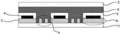
其中,如图1、2所示,根据图1在A-A’方向上的截面可以得出图2所示的Frit部分平面透视结构示意图,其中如图2所示在玻璃基板1的缓冲层3上设置有凹孔区域a和非凹孔区域b,在非凹孔区域b设置有金属层4和绝缘层=5;通过Frit材料6将玻璃基板1与待封装玻璃2粘结在一起;其中,虽然在玻璃基板1上的缓冲层3设置有凹孔区域a,可是在对OLED显示器件Frit封装技术信赖性测试中发现,对出现不良(英文全称:Not Given,简称:NG)的OLED显示器件进行解析时,大部分的封装漏气OLED显示器件是由于Frit材料在非凹孔区域b发生了位移脱落断裂。研究后发现,非凹孔区域b的表面与非凹孔区域b和Frit材料6的接触面是平行的,通过Frit材料6的粘结,只是在水平方向上进行了粘接;Frit材料6在未固化前,在外部环境的影响下,在非凹孔区域b的表面与非凹孔区域b和Frit材料6的接触面就很容易发生位移,导致位于非凹孔区域b表面上的Frit材料6脱落断裂,从而导致OLED显示器件被水氧侵蚀。总之,现有技术中采用封框胶对显示器件中玻璃基板与待封装基板封装时,存在封框胶脱落断裂的概率从而造成显示器件被水氧侵蚀的问题。Among them, as shown in Figures 1 and 2, according to the cross-section of Figure 1 in the AA' direction, a schematic perspective view of the Frit part shown in Figure 2 can be obtained. As shown in Figure 2, the buffer layer of the glass substrate 1 3 is provided with a concave hole area a and a non-concave hole area b, and a
发明内容SUMMARY OF THE INVENTION
本发明的实施例提供一种显示基板及制作方法和显示设备,能够降低封框胶脱落断裂的概率,解决封框胶脱落断裂造成OLED显示器件被水氧侵蚀的问题。Embodiments of the present invention provide a display substrate, a manufacturing method, and a display device, which can reduce the probability of the sealant falling off and breaking, and solve the problem that the OLED display device is eroded by water and oxygen caused by the falling off and breaking of the frame sealant.
为达到上述目的,本发明的实施例采用如下技术方案:To achieve the above object, the embodiments of the present invention adopt the following technical solutions:
第一方面、本发明实施例提供一种显示基板,显示基板上设置有功能膜层,在至少一层功能膜层的远离显示基板的一侧包括凸出阵列;其中,显示基板与另一显示基板对盒时,凸出阵列对应的凸起用于嵌入显示基板与另一显示基板之间的封框胶。In a first aspect, an embodiment of the present invention provides a display substrate, the display substrate is provided with a functional film layer, and a side of at least one functional film layer away from the display substrate includes a protruding array; wherein the display substrate and another display When the substrates are assembled into boxes, the protrusions corresponding to the protruding arrays are used to embed the frame sealant between the display substrate and another display substrate.
具体的,凸出阵列由凸出子阵列排列形成;每个凸出子阵列包括平坦部分以及设置于平坦部分上的至少一个凸起部分。Specifically, the protruding array is formed by arranging protruding sub-arrays; each protruding sub-array includes a flat portion and at least one protruding portion disposed on the flat portion.
具体的,功能膜层包括第一功能膜层、第二功能膜层;第一功能膜层的一侧与显示基板接触,第二功能膜层的一侧与第一功能膜层的另一侧接触;第二功能膜层包括凸出阵列;在第二功能膜层上远离显示基板的一侧形成有凸出阵列;其中,平坦部分以及设置于平坦部分上的至少一个凸起部分位于第一功能膜层上。Specifically, the functional film layer includes a first functional film layer and a second functional film layer; one side of the first functional film layer is in contact with the display substrate, and one side of the second functional film layer is in contact with the other side of the first functional film layer contact; the second functional film layer includes a protruding array; a protruding array is formed on the side of the second functional film layer away from the display substrate; wherein the flat part and at least one protruding part arranged on the flat part are located on the first on the functional membrane.
具体的,在第一功能膜层的远离显示基板的一侧设置有凸出阵列。Specifically, a protruding array is provided on the side of the first functional film layer away from the display substrate.
具体的,功能膜层还包括第三功能膜层;Specifically, the functional film layer further includes a third functional film layer;
第三功能膜层覆盖平坦部分,且第三功能膜层的厚度小于凸起部分的厚度;第三功能膜层上设置有至少一个过孔,设置于平坦部分上的至少一个凸起部分的顶部穿过过孔。The third functional film layer covers the flat part, and the thickness of the third functional film layer is smaller than the thickness of the convex part; the third functional film layer is provided with at least one via hole, which is provided on the top of the at least one convex part on the flat part through the via.
具体的,功能膜层还包括第三功能膜层;Specifically, the functional film layer further includes a third functional film layer;
第三功能膜层覆盖平坦部分和设置于平坦部分上的凸起部分。The third functional film layer covers the flat portion and the convex portion provided on the flat portion.
具体的,第三功能膜层包括与第一功能膜层接触的部分。Specifically, the third functional film layer includes a portion in contact with the first functional film layer.
具体的,至少一层功能膜层包括凹孔区域和非凹孔区域;凸出阵列位于非凹孔区域。Specifically, at least one functional film layer includes a concave hole area and a non-concave hole area; the protruding array is located in the non-concave hole area.
具体的,凸起部分的截面至少为以下一种形状:圆形、三角形、矩形和多边形;Specifically, the cross section of the raised portion is at least one of the following shapes: circle, triangle, rectangle and polygon;
具体的,凸起部分的顶部为弧面。Specifically, the top of the raised portion is an arc surface.
具体的,平坦部分以及设置于平坦部分上的至少一个凸起部分为金属。Specifically, the flat portion and the at least one protruding portion disposed on the flat portion are metal.
具体的,第一功能膜层为缓冲层,缓冲层的材料包含SiNx或者SiO2的至少一种。Specifically, the first functional film layer is a buffer layer, and the material of the buffer layer includes at least one of SiNx or SiO2.
具体的,第二功能膜层为金属层。Specifically, the second functional film layer is a metal layer.
具体的,第三功能膜层为绝缘层;绝缘层的材料包含SiNx或者SiO2的至少一种。Specifically, the third functional film layer is an insulating layer; the material of the insulating layer includes at least one of SiNx or SiO2.
第二方面、本发明实施例提供一种显示基板的制作方法,包括如下:In a second aspect, an embodiment of the present invention provides a method for manufacturing a display substrate, including the following:
在显示基板上形成至少一层功能膜层;forming at least one functional film layer on the display substrate;
在至少一层功能膜层远离显示基板的一侧形成凸出阵列;其中,显示基板与另一显示基板对盒时,凸出阵列对应的凸起用于嵌入显示基板与另一显示基板之间的封框胶。A protrusion array is formed on the side of at least one functional film layer away from the display substrate; wherein, when the display substrate and another display substrate are assembled, the protrusions corresponding to the protrusion array are used to embed the protrusions between the display substrate and the other display substrate. Frame sealant.
具体的,功能膜层包括第一功能膜层,在显示基板上制作第一功能膜层包括如下步骤:Specifically, the functional film layer includes a first functional film layer, and the fabrication of the first functional film layer on the display substrate includes the following steps:
在显示基板上利用沉积工艺形成第一功能膜层;using a deposition process to form a first functional film layer on the display substrate;
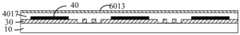
在第一功能膜层上涂覆第一光刻胶层,并进行第一次曝光显影,在第一光刻胶层上形成凹孔区域与非凹孔区域的图案;Coating a first photoresist layer on the first functional film layer, and performing the first exposure and development, and forming a pattern of a concave hole area and a non-concave hole area on the first photoresist layer;
在第一次曝光显影后的显示基板上通过刻蚀工艺在第一功能膜层上形成凹孔区域与非凹孔区域,并剥离第一光刻胶层。On the display substrate after the first exposure and development, a concave hole area and a non-concave hole area are formed on the first functional film layer by an etching process, and the first photoresist layer is peeled off.
具体的,在功能膜层远离显示基板的一侧形成凸出阵列包括如下步骤:Specifically, forming a protruding array on the side of the functional film layer away from the display substrate includes the following steps:
形成第一功能膜层;forming a first functional film layer;
在形成第一功能膜层的显示基板上通过沉积工艺制备第一材料层;preparing a first material layer by a deposition process on the display substrate on which the first functional film layer is formed;
涂覆覆盖第一材料层的第二光刻胶层,并进行第二次曝光显影,在第二光刻胶层上第一功能膜层的非凹孔区域对应的位置形成平坦部分的图案;coating a second photoresist layer covering the first material layer, and performing a second exposure and development to form a pattern of a flat portion on the second photoresist layer at a position corresponding to the non-concave area of the first functional film layer;
在第二次曝光显影后的显示基板通过刻蚀工艺在第一材料层上形成平坦部分,并剥离第二光刻胶层;After the second exposure and development of the display substrate, a flat portion is formed on the first material layer by an etching process, and the second photoresist layer is peeled off;
在形成平坦部分的显示基板上通过沉积工艺制备第三材料层;preparing a third material layer by a deposition process on the display substrate forming the flat portion;
涂覆覆盖第三材料层的第三光刻胶层,并进行第三次曝光显影,在第三光刻胶层上平坦部分对应的位置形成第三功能膜层的图案;Coating the third photoresist layer covering the third material layer, and performing the third exposure and development, and forming the pattern of the third functional film layer on the position corresponding to the flat portion on the third photoresist layer;
在第三次曝光显影后的显示基板通过刻蚀工艺形成第三功能膜层,并剥离第三光刻胶层;其中,第三功能膜层覆盖平坦部分;After the third exposure and development of the display substrate, a third functional film layer is formed by an etching process, and the third photoresist layer is peeled off; wherein, the third functional film layer covers the flat portion;
涂覆覆盖第三功能膜层的第四光刻胶层,并进行第四次曝光显影,在第四光刻胶层上形成过孔的图案;Coating a fourth photoresist layer covering the third functional film layer, and performing a fourth exposure and development to form a pattern of vias on the fourth photoresist layer;
在第四次曝光显影后的显示基板通过刻蚀工艺在第三功能膜层上形成过孔;A via hole is formed on the third functional film layer through an etching process on the display substrate after the fourth exposure and development;
在形成过孔的显示基板上制备第二材料层,第二材料层通过过孔与平坦部分连接;preparing a second material layer on the display substrate with the via hole formed, and the second material layer is connected with the flat part through the via hole;
涂覆覆盖第二材料层的第五光刻胶层,并进行第五次曝光显影,在第五光刻胶层上保留凸起部分对应的光刻胶;Coating the fifth photoresist layer covering the second material layer, and performing the fifth exposure and development, and retaining the photoresist corresponding to the raised portion on the fifth photoresist layer;
在第五次曝光显影后的显示基板通过刻蚀工艺在第二材料层上形成凸起部分,并剥离第四光刻胶层和第五光刻胶层,形成包含平坦部分和设置于平坦部分上的凸起部分的第二功能膜层。After the fifth exposure and development of the display substrate, a raised portion is formed on the second material layer by an etching process, and the fourth photoresist layer and the fifth photoresist layer are peeled off to form a flat portion and a flat portion disposed on the flat portion. The second functional film layer on the raised part.
具体的,在第五光刻胶层上保留凸起部分对应的光刻胶与凸起部分顶部的形状相同。Specifically, the photoresist corresponding to the raised portion remains on the fifth photoresist layer and has the same shape as the top of the raised portion.
具体的,凸起部分的顶部为弧面时,弧面用于反射固化光线。Specifically, when the top of the raised portion is an arc surface, the arc surface is used to reflect curing light.
具体的,在功能膜层远离显示基板的一侧形成凸出阵列包括如下步骤:Specifically, forming a protruding array on the side of the functional film layer away from the display substrate includes the following steps:
形成第一功能膜层;在形成第一功能膜层的显示基板上通过沉积工艺制备第一材料层;forming a first functional film layer; preparing a first material layer by a deposition process on the display substrate on which the first functional film layer is formed;
涂覆覆盖第一材料层的第二光刻胶层,并进行第二次曝光显影,在第二光刻胶层上第一功能膜层的非凹孔区域对应的位置形成平坦部分的图案;coating a second photoresist layer covering the first material layer, and performing a second exposure and development to form a pattern of a flat portion on the second photoresist layer at a position corresponding to the non-concave area of the first functional film layer;
在第二次曝光显影后的显示基板通过刻蚀工艺在第一材料层上形成平坦部分,并剥离第二光刻胶层;After the second exposure and development of the display substrate, a flat portion is formed on the first material layer by an etching process, and the second photoresist layer is peeled off;
涂覆覆盖平坦部分的第三光刻胶层,并通过第三次曝光显影,在第三光刻胶层上平坦部分的凸起部分对应的位置形成过孔的图案;Coating a third photoresist layer covering the flat portion, and through the third exposure and development, a pattern of via holes is formed on the third photoresist layer at the position corresponding to the convex portion of the flat portion;
在第三次曝光显影后的显示基板上通过沉积工艺在第三光刻胶层上形成第二材料层;其中第二材料层通过过孔与平坦部分连接;A second material layer is formed on the third photoresist layer by a deposition process on the display substrate after the third exposure and development; wherein the second material layer is connected to the flat portion through a via hole;
涂覆覆盖第二材料层的第四光刻胶层,并进行第四次曝光显影,在第四光刻胶层上保留凸起部分对应的光刻胶;Coating the fourth photoresist layer covering the second material layer, and performing the fourth exposure and development, and retaining the photoresist corresponding to the raised portion on the fourth photoresist layer;
在第四次曝光显影后的显示基板通过刻蚀工艺在第二材料层上形成凸起部分,并剥离第三光刻胶层和第四光刻胶层,形成包含平坦部分和设置与平坦部分上的凸起部分的第二功能膜层;After the fourth exposure and development of the display substrate, a raised portion is formed on the second material layer by an etching process, and the third photoresist layer and the fourth photoresist layer are peeled off to form a flat portion and a set and flat portion. the second functional film layer on the raised portion;
在第四次曝光显影后的显示基板上通过沉积工艺形成覆盖第二功能膜层的第三材料层;forming a third material layer covering the second functional film layer on the display substrate after the fourth exposure and development by a deposition process;
涂覆覆盖第三材料层的第五光刻胶层,并进行第五次曝光显影,在第五光刻胶层上形成第三功能膜层的图案;Coating the fifth photoresist layer covering the third material layer, and performing the fifth exposure and development to form the pattern of the third functional film layer on the fifth photoresist layer;
在第五次曝光显影后的显示基板通过刻蚀工艺在第三材料层上形成第三功能膜层,并剥离第五光刻胶层。After the fifth exposure and development of the display substrate, a third functional film layer is formed on the third material layer through an etching process, and the fifth photoresist layer is peeled off.
具体的,在第四光刻胶层上保留的凸起部分对应的光刻胶与凸起部分顶部的形状相同。Specifically, the photoresist corresponding to the raised portion remaining on the fourth photoresist layer has the same shape as the top of the raised portion.
具体的,凸起部分的顶部为弧面时,弧面用于反射固化光线。Specifically, when the top of the raised portion is an arc surface, the arc surface is used to reflect curing light.
第三方面、本发明实施例提供一种显示设备,包含权利要求第一方面提供的任一显示基板。In a third aspect, an embodiment of the present invention provides a display device including any display substrate provided in the first aspect of the claim.
本发明的实施例提供一种显示基板,通过在显示基板上设置有功能膜层,在至少一层功能膜层的远离显示基板的一侧包括凸出阵列,并将凸出阵列的凸起嵌入封框胶中,使得显示基板与另一个显示基板通过封框胶粘结时,由于凸出阵列的凸起嵌入了封框胶中,这就会增加一个防止功能膜层远离显示基板的一侧和封框胶的接触面发生位移的作用力,即增大了平行方向上的固定作用,能够阻止功能膜层远离显示基板的一侧与封框胶的接触面之间发生位移,进而能够降低由于位移造成的封框胶脱落断裂的概率,解决封框胶脱落断裂造成显示器件被水氧侵蚀的问题。此外,由于在至少一层功能膜层的远离显示基板的一侧设置有凸出阵列,并将凸出阵列嵌入封框胶中,使得功能膜层远离显示基板的一侧与封框胶的接触面积相比现有技术中功能膜层远离显示基板的一侧与封框胶的接触面积更大,所以使得功能膜层远离显示基板的一侧与封框胶之间的粘结牢固程度,进而增加了封框胶在显示基板与另一显示基板中的粘结牢固程度。An embodiment of the present invention provides a display substrate. By disposing a functional film layer on the display substrate, at least one functional film layer includes a protruding array on the side away from the display substrate, and embeds the protrusions of the protruding array. In the frame sealing glue, when the display substrate and another display substrate are bonded by the frame sealing glue, since the protrusions of the protruding array are embedded in the frame sealing glue, this will add a side that prevents the functional film layer from being far away from the display substrate. The force of displacement of the contact surface with the frame sealant increases the fixing effect in the parallel direction, which can prevent the displacement between the side of the functional film layer away from the display substrate and the contact surface of the frame sealant, thereby reducing the The probability of the frame sealant falling off and breaking due to displacement can solve the problem that the display device is corroded by water and oxygen caused by the frame sealant falling off and breaking. In addition, since a protruding array is provided on the side of at least one functional film layer away from the display substrate, and the protruding array is embedded in the sealant, the side of the functional film layer away from the display substrate is in contact with the sealant. Compared with the prior art, the contact area of the side of the functional film layer away from the display substrate and the frame sealant is larger, so the bonding firmness between the side of the functional film layer away from the display substrate and the frame sealant is made, and then The bonding firmness of the frame sealant between the display substrate and another display substrate is increased.
附图说明Description of drawings
为了更清楚地说明本发明实施例或现有技术中的技术方案,下面将对实施例或现有技术描述中所需要使用的附图作简单地介绍,显而易见地,下面描述中的附图仅仅是本发明的一些实施例,对于本领域普通技术人员来讲,在不付出创造性劳动的前提下,还可以根据这些附图获得其他的附图。In order to explain the embodiments of the present invention or the technical solutions in the prior art more clearly, the following briefly introduces the accompanying drawings that need to be used in the description of the embodiments or the prior art. Obviously, the accompanying drawings in the following description are only These are some embodiments of the present invention. For those of ordinary skill in the art, other drawings can also be obtained according to these drawings without creative efforts.
图1为现有技术中Frit部分平面透视结构示意图;Fig. 1 is a schematic diagram of a plane perspective structure of the Frit part in the prior art;
图2为现有技术中图1中A-A’的截面示意图;Fig. 2 is the cross-sectional schematic diagram of A-A' in Fig. 1 in the prior art;
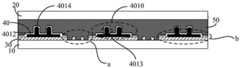
图3为本发明实施例提供的一种显示器件的具体显示基板的平面透视结构示意图;3 is a schematic perspective view of a plane structure of a specific display substrate of a display device according to an embodiment of the present invention;
图4为本发明实施例提供的如图3所示的显示器件的显示基板的B-B’的截面示意图;FIG. 4 is a schematic cross-sectional view of B-B' of the display substrate of the display device shown in FIG. 3 according to an embodiment of the present invention;
图5为本发明实施例提供的如图3所示的显示器件的另一种显示基板的B-B’的截面示意图;Fig. 5 is a schematic cross-sectional view of B-B' of another display substrate of the display device shown in Fig. 3 according to an embodiment of the present invention;
图6为本发明实施例提供的一种显示基板凸起部分顶部示意图;6 is a top schematic diagram of a convex portion of a display substrate according to an embodiment of the present invention;
图7为本发明实施例提供的一种显示基板的制作方法的具体步骤流程图;FIG. 7 is a flow chart of specific steps of a method for manufacturing a display substrate provided by an embodiment of the present invention;
图8-a-8-p为本发明实施例提供的一种显示基板的制作过程中的结构示意图;8-a-8-p are schematic structural diagrams in a manufacturing process of a display substrate according to an embodiment of the present invention;
图9为本发明实施例提供的一种显示基板的另一种制作方法的具体步骤的流程图;9 is a flowchart of specific steps of another method for manufacturing a display substrate according to an embodiment of the present invention;
图10-a-10-q为本发明实施例提供的一种显示基板的另一种制作过程中的结构示意图。10-a-10-q are schematic structural diagrams of another manufacturing process of a display substrate according to an embodiment of the present invention.
附图标记:Reference number:
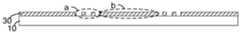
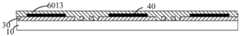
10-显示基板;10-Display substrate;
20-另一显示基板;20-another display substrate;
30-第一功能膜层;30 - the first functional film layer;
40-第二功能膜层;40 - the second functional film layer;
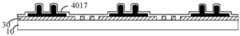
4010-凸出阵列;4011-平坦部分;4012-第三功能膜层;4013-过孔;4014-凸起部分;4015-第一材料层;4016-第二材料层;4017-第三材料层;4010-protrusion array; 4011-flat part; 4012-third functional film layer; 4013-via hole; 4014-protrusion part; 4015-first material layer; 4016-second material layer; 4017-third material layer ;
50-封框胶;50-frame sealant;
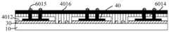
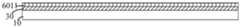
6011-第一光刻胶层;6012第二光刻胶层;6013-第三光刻胶层;6014-第四光刻胶层;6015-第五光刻胶层;6011 - the first photoresist layer; 6012 - the second photoresist layer; 6013 - the third photoresist layer; 6014 - the fourth photoresist layer; 6015 - the fifth photoresist layer;
a-凹孔区域;b-非凹孔区域。a-recessed area; b-non-recessed area.
具体实施方式Detailed ways
下面将结合本发明实施例中的附图,对本发明实施例中的技术方案进行清楚、完整地描述,显然,所描述的实施例仅仅是本发明一部分实施例,而不是全部的实施例。基于本发明中的实施例,本领域普通技术人员在没有做出创造性劳动前提下所获得的所有其他实施例,都属于本发明保护的范围。The technical solutions in the embodiments of the present invention will be clearly and completely described below with reference to the accompanying drawings in the embodiments of the present invention. Obviously, the described embodiments are only a part of the embodiments of the present invention, but not all of the embodiments. Based on the embodiments of the present invention, all other embodiments obtained by those of ordinary skill in the art without creative efforts shall fall within the protection scope of the present invention.
本发明的实施例提供一种显示基板,通过在显示基板上设置有功能膜层,在至少一层功能膜层的远离显示基板的一侧包括凸出阵列,并将凸出阵列的凸起嵌入封框胶中,使得显示基板与另一个显示基板通过封框胶粘结时,由于凸出阵列的凸起嵌入了封框胶中,这就会增加一个防止功能膜层远离显示基板的一侧和封框胶的接触面发生位移的作用力,即增大了平行方向上的固定作用,能够阻止功能膜层远离显示基板的一侧与封框胶的接触面之间发生位移,进而能够降低由于位移造成的封框胶脱落断裂的概率,解决封框胶脱落断裂造成显示器件被水氧侵蚀的问题。此外,由于在至少一层功能膜层的远离显示基板的一侧设置有凸出阵列,并将凸出阵列嵌入封框胶中,使得功能膜层远离显示基板的一侧与封框胶的接触面积相比现有技术中功能膜层远离显示基板的一侧与封框胶的接触面积更大,所以使得功能膜层远离显示基板的一侧与封框胶之间的粘结牢固程度,进而增加了封框胶在显示基板与另一显示基板中的粘结牢固程度。An embodiment of the present invention provides a display substrate. By disposing a functional film layer on the display substrate, at least one functional film layer includes a protruding array on the side away from the display substrate, and embeds the protrusions of the protruding array. In the frame sealing glue, when the display substrate and another display substrate are bonded by the frame sealing glue, since the protrusions of the protruding array are embedded in the frame sealing glue, this will add a side that prevents the functional film layer from being far away from the display substrate. The force of displacement of the contact surface with the frame sealant increases the fixing effect in the parallel direction, which can prevent the displacement between the side of the functional film layer away from the display substrate and the contact surface of the frame sealant, thereby reducing the The probability of the frame sealant falling off and breaking due to displacement can solve the problem that the display device is corroded by water and oxygen caused by the frame sealant falling off and breaking. In addition, since a protruding array is provided on the side of at least one functional film layer away from the display substrate, and the protruding array is embedded in the sealant, the side of the functional film layer away from the display substrate is in contact with the sealant. Compared with the prior art, the contact area of the side of the functional film layer away from the display substrate and the frame sealant is larger, so the bonding firmness between the side of the functional film layer away from the display substrate and the frame sealant is made, and then The bonding firmness of the frame sealant between the display substrate and another display substrate is increased.
实施例一、本发明实施例提供一种显示基板,如图3、4所示,显示基板10上设置有功能膜层,在至少一层功能膜层的远离显示基板10的一侧包括凸出阵列4010,其中,显示基板10与另一显示基板20对盒时,凸出阵列4010对应的凸起用于嵌入显示基板10与另一显示基板20之间的封框胶50。Embodiment 1. The embodiment of the present invention provides a display substrate. As shown in FIGS. 3 and 4 , the
由上述可知,根据图3在B-B’方向上的截面可以得出图4所示的显示基板的具体的平面透视结构示意图,其中如图4所示通过在显示基板上设置有功能膜层,在至少一层功能膜层的远离显示基板的一侧包括凸出阵列,并将凸出阵列的凸起嵌入封框胶中,使得显示基板与另一显示基板通过封框胶粘结时,由于凸出阵列的凸起嵌入了封框胶中,这就会增加一个防止功能膜层远离显示基板的一侧和封框胶的接触面发生位移的作用力,即增大了平行方向上的固定作用,能够阻止功能膜层远离显示基板的一侧与封框胶的接触面之间发生位移,进而能够降低由于位移造成的封框胶脱落断裂的概率,解决封框胶脱落断裂造成显示器件被水氧侵蚀的问题。此外,由于在至少一层功能膜层的远离显示基板的一侧设置有凸出阵列,并将凸出阵列嵌入封框胶中,使得功能膜层远离显示基板的一侧与封框胶的接触面积相比现有技术中功能膜层远离显示基板的一侧与封框胶的接触面积更大,所以使得功能膜层远离显示基板的一侧与封框胶之间的粘结牢固程度,进而增加了封框胶在显示基板与另一显示基板中的粘结牢固程度。As can be seen from the above, according to the cross-section of FIG. 3 in the BB' direction, a specific schematic plane perspective structure of the display substrate shown in FIG. 4 can be obtained. As shown in FIG. 4, a functional film layer is provided on the display substrate as shown in FIG. , the side of at least one functional film layer away from the display substrate includes a protruding array, and the protrusions of the protruding array are embedded in the frame sealant, so that when the display substrate and another display substrate are bonded by the frame sealant, Since the protrusions of the protruding array are embedded in the sealant, this will increase a force that prevents the side of the functional film layer away from the display substrate and the contact surface of the sealant from being displaced, that is, it increases the force in the parallel direction. The fixing effect can prevent the displacement between the side of the functional film layer away from the display substrate and the contact surface of the frame sealant, thereby reducing the probability of the frame sealant falling off and breaking due to displacement, and solving the display device caused by the frame sealant falling off and breaking. The problem of erosion by water and oxygen. In addition, since a protruding array is provided on the side of at least one functional film layer away from the display substrate, and the protruding array is embedded in the sealant, the side of the functional film layer away from the display substrate is in contact with the sealant. Compared with the prior art, the contact area of the side of the functional film layer away from the display substrate and the frame sealant is larger, so the bonding firmness between the side of the functional film layer away from the display substrate and the frame sealant is made, and then The bonding firmness of the frame sealant between the display substrate and another display substrate is increased.
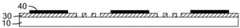
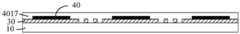
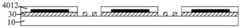
实施例二、一种显示基板,如图3、图4和图6所示,其中:凸出阵列4010由凸出子阵列排列形成;每个凸出子阵列包括平坦部分4011以及设置于平坦部分上的至少一个凸起部分4014。
具体的,所述功能膜层包括第一功能膜层30、第二功能膜层40;所述第一功能膜层30的一侧与所述显示基板10接触,所述第二功能膜层40的一侧与所述第一功能膜层30的另一侧接触;所述第二功能膜层40包括所述凸出阵列4010;在所述第二功能膜层40上远离所述显示基板10的一侧形成有凸出阵列4010;其中,所述平坦部分4011以及设置于所述平坦部分4011上的至少一个凸起部分4014位于所述第一功能膜层30上。Specifically, the functional film layer includes a first
具体的,在所述第一功能膜层30的远离所述显示基板10的一侧设置有所述凸出阵列4010。Specifically, the protruding
具体的,所述功能膜层还包括第三功能膜层4012;Specifically, the functional film layer further includes a third
所述第三功能膜层4012覆盖所述平坦部分4014,且所述第三功能膜层4012的厚度小于所述凸起部分4014的厚度;所述第三功能膜层4012上设置有至少一个过孔4013,所述设置于所述平坦部分4011上的至少一个凸起部分4014的顶部穿过所述过孔4013。The third
需要说明的是,这里凸起部分的顶部可以嵌入封框胶中。It should be noted that the top of the raised portion can be embedded in the frame sealant.
具体的,所述第三功能膜层4012包括与所述第一功能膜层30接触的部分。Specifically, the third
具体的,至少一层所述功能膜层包括凹孔区域a和非凹孔区域b;所述凸出阵列4010位于所述非凹孔区域b。Specifically, at least one layer of the functional film layer includes a concave hole area a and a non-concave hole area b; the
具体的,所述凸起部分4014的截面至少为以下一种形状:圆形、三角形、矩形和多边形,所述凸起部分4014的顶部为弧面。Specifically, the cross section of the raised
具体的,所述平坦部分4011以及设置于平坦部分4011上的至少一个凸起部分4014为金属。Specifically, the flat portion 4011 and at least one protruding
需要说明的是,平坦部分以及设置于平坦部分上的至少一个凸起部分的制备材料可以为钼。It should be noted that, the preparation material of the flat portion and the at least one convex portion disposed on the flat portion may be molybdenum.
具体的,所述第一功能膜层30为缓冲层,所述缓冲层的材料包含SiNx或者SiO2的至少一种。Specifically, the first
具体的,所述第二功能膜层40为金属层。Specifically, the second
具体的,所述第三功能膜层4012为绝缘层;所述绝缘层的材料包含SiNx或者SiO2的至少一种。Specifically, the third
需要说明的是,在实际制备过程中,由于直接将第二功能膜层设置在显示基板上时,显示基板对第二功能膜层的固定作用不够;因此,需要在显示基板上首先设置第一功能膜层,由于第一功能膜层可以很好的与显示基板之间的结合力很强,并且金属层和第一功能膜层之间的结合力也很好,这样就可以很好的固定产品,增加产品的稳定性。It should be noted that, in the actual preparation process, when the second functional film layer is directly arranged on the display substrate, the fixing effect of the display substrate on the second functional film layer is not enough; The functional film layer, because the first functional film layer can have a good bonding force with the display substrate, and the bonding force between the metal layer and the first functional film layer is also very good, so that the product can be well fixed , to increase the stability of the product.
由上述可知,根据图3在B-B’方向上的截面可以得出图4所示的显示基板的平面透视结构示意图,其中如图4所示凸出阵列由若干个凸出子阵列组成,其中每个凸出子阵列包括平坦部分以及设置于平坦部分上的至少一个凸起部分组成;制备第三功能膜层与第一功能膜层的材料可以为SiNx或者SiO2中的至少一种,设置于平坦部分上的至少一个凸起部分是通过设置在第三功能膜层上的过孔,将凸起部分的顶部嵌入封框胶中;其中,平坦部分以及设置于平坦部分上的至少一个凸起部分形成的材料为金属;形成的凸起部分的截面可以根据实际的需要,制备成不同的形状,如圆形;如图6所示,当凸起部分的顶部为弧形时,这样就可以在激光密封时,通过凸起部分顶部的弧形来反射激光光线;现有技术中,因为发射激光光线的装置位于第一基板上的上方,所以位于第一功能膜层非凹孔区域表面的封框胶只能接收到垂直方向上的激光光线;而本发明实施例提供凸出子阵列中的凸起部分的顶部为弧形,这样可以使得位于凸起部分周围的封框胶不仅接收到垂直方向上的激光光线而且还可以接收到弧形表面所反射的激光光线,从而使得位于凸起部分周围的封框胶在同样的时间内所接收到的激光光线更多,即激光的能量更多,进而使得封框胶的熔融状态更好。As can be seen from the above, according to the cross-section of FIG. 3 in the BB' direction, a schematic plan perspective structure of the display substrate shown in FIG. 4 can be obtained, wherein the protruding array shown in FIG. 4 is composed of several protruding sub-arrays, Wherein each protruding sub-array comprises a flat part and at least one protruding part arranged on the flat part; the material for preparing the third functional film layer and the first functional film layer can be at least one of SiNx or SiO2, and the set At least one protruding part on the flat part is through the via hole arranged on the third functional film layer, and the top of the protruding part is embedded in the frame sealant; wherein, the flat part and the at least one protruding part arranged on the flat part are The material of the raised part is metal; the cross-section of the raised part can be prepared into different shapes according to actual needs, such as a circle; as shown in Figure 6, when the top of the raised part is arc-shaped, so During laser sealing, the laser light can be reflected by the arc at the top of the convex part; in the prior art, because the device for emitting laser light is located above the first substrate, it is located on the surface of the non-concave area of the first functional film layer The frame sealant can only receive the laser light in the vertical direction; and the embodiment of the present invention provides that the top of the protruding part in the protruding sub-array is arc-shaped, so that the frame sealant around the protruding part can not only receive The laser light in the vertical direction can also receive the laser light reflected by the curved surface, so that the frame sealant around the convex part can receive more laser light in the same time, that is, the energy of the laser more, which in turn makes the melting state of the sealant better.
需要说明的是凸出子阵列至少可以包含一个凸起部分。其中如图3所示,凹孔区域为阵列排布,凸出阵列围绕凹孔区域分布。It should be noted that the protruding sub-array may include at least one protruding portion. As shown in FIG. 3 , the concave hole area is arranged in an array, and the protruding array is distributed around the concave hole area.
实施例三、一种显示基板,如图3、图5和图6所示,其中:凸出阵列4010由凸出子阵列排列形成;每个凸出子阵列包括平坦部分4011以及设置于平坦部分上的至少一个凸起部分4014。
具体的,所述功能膜层包括第一功能膜层30、第二功能膜层40;所述第一功能膜层30的一侧与所述显示基板10接触,所述第二功能膜层40的一侧与所述第一功能膜层30的另一侧接触;所述第二功能膜层40包括所述凸出阵列4010;在所述第二功能膜层40上远离所述显示基板10的一侧形成有凸出阵列4010;其中,所述平坦部分4011以及设置于所述平坦部分4011上的至少一个凸起部分4014位于所述第一功能膜层30上。Specifically, the functional film layer includes a first
具体的,在所述第一功能膜层30的远离所述显示基板10的一侧设置有所述凸出阵列4010。Specifically, the protruding
具体的,所述功能膜层还包括第三功能膜层4012;Specifically, the functional film layer further includes a third
所述第三功能膜层4012覆盖所述平坦部分4014,且所述第三功能膜层4012的厚度小于所述凸起部分4014的厚度;所述第三功能膜层4012上设置有至少一个过孔4013,所述设置于所述平坦部分4011上的至少一个凸起部分4014的顶部穿过所述过孔4013。The third
需要说明的是,这里凸起部分的顶部可以嵌入封框胶中。It should be noted that the top of the raised portion can be embedded in the frame sealant.
具体的,所述第三功能膜层4012包括与所述第一功能膜层30接触的部分。Specifically, the third
具体的,至少一层所述功能膜层包括凹孔区域a和非凹孔区域b;所述凸出阵列4010位于所述非凹孔区域b。Specifically, at least one layer of the functional film layer includes a concave hole area a and a non-concave hole area b; the
具体的,所述凸起部分4014的截面至少为以下一种形状:圆形、三角形、矩形和多边形,所述凸起部分4014的顶部为弧面。Specifically, the cross section of the raised
具体的,所述平坦部分4011以及设置于平坦部分4011上的至少一个凸起部分4014为金属。Specifically, the flat portion 4011 and at least one protruding
需要说明的是,平坦部分以及设置于平坦部分上的至少一个凸起部分的制备材料可以为钼。It should be noted that, the preparation material of the flat portion and the at least one convex portion disposed on the flat portion may be molybdenum.
具体的,所述第一功能膜层30为缓冲层,所述缓冲层的材料包含SiNx或者SiO2的至少一种。Specifically, the first
具体的,所述第二功能膜层40为金属层。Specifically, the second
具体的,所述第三功能膜层4012为绝缘层;所述绝缘层的材料包含SiNx或者SiO2的至少一种。Specifically, the third
需要说明的是,在实际制备过程中,由于直接将第二功能膜层设置在显示基板上时,显示基板对第二功能膜层的固定作用不够;因此,需要在显示基板上首先设置第一功能膜层,由于第一功能膜层可以很好的与显示基板之间的结合力很强,并且金属层和第一功能膜层之间的结合力也很好,这样就可以很好的固定产品,增加产品的稳定性。It should be noted that, in the actual preparation process, when the second functional film layer is directly arranged on the display substrate, the fixing effect of the display substrate on the second functional film layer is not enough; The functional film layer, because the first functional film layer can have a good bonding force with the display substrate, and the bonding force between the metal layer and the first functional film layer is also very good, so that the product can be well fixed , to increase the stability of the product.
由上述可知,根据图3在B-B’方向上的截面可以得出图5所示的显示器基板的平面透视结构示意图,其中如图5所示凸出阵列由若干个凸出子阵列组成,其中每个凸出子阵列包括平坦部分以及设置于平坦部分上的至少一个凸起部分组成;制备第三功能膜层与第一功能膜层的材料可以为SiNx或者SiO2中的至少一种,其中第三功能膜层设置在第一功能膜层上,并覆盖平坦部分和设置于平坦部分上的凸起部分;其中,平坦部分以及设置于平坦部分上的至少一个凸起部分形成的材料为金属;形成的凸起部分的截面可以根据实际的需要,制备成不同的形状。As can be seen from the above, according to the cross section of FIG. 3 in the BB' direction, a schematic plane perspective structure of the display substrate shown in FIG. 5 can be obtained, wherein the protruding array as shown in FIG. 5 is composed of several protruding sub-arrays, Wherein each protruding sub-array comprises a flat part and at least one protruding part arranged on the flat part; the material for preparing the third functional film layer and the first functional film layer can be at least one of SiNx or SiO2, wherein The third functional film layer is disposed on the first functional film layer, and covers the flat portion and the convex portion disposed on the flat portion; wherein, the material of the flat portion and at least one convex portion disposed on the flat portion is metal ; The cross-section of the formed raised portion can be prepared into different shapes according to actual needs.
需要说明的是凸出子阵列至少可以包含一个凸起部分。其中如图3所示,凹孔区域为阵列排布,凸出阵列围绕凹孔区域分布。It should be noted that the protruding sub-array may include at least one protruding portion. As shown in FIG. 3 , the concave hole area is arranged in an array, and the protruding array is distributed around the concave hole area.
其中,这里的嵌入封框胶中的凸起为设置于第一功能膜层上的第三功能膜层,其中,第三功能膜层覆盖平坦部分和设置于平坦部分上的凸起部分,在对应设置于平坦部分上的凸起部分上方的第三功能膜层上形成了凸出阵列的凸起,并将设置于平坦部分上的凸起部分上方的第三功能膜层上形成的凸出阵列的凸起嵌入封框胶中,使得显示基板与另一显示基板通过封框胶粘结时,由于凸出阵列的凸起部分嵌入了封框胶中,这就会增加一个防止第三功能膜层的表面与第三功能膜层和封框胶的接触面发生位移的作用力,即增大了平行方向上的固定作用,能够阻止第三功能膜层与封框胶的接触面之间发生位移,进而能够降低由于位移造成的封框胶脱落断裂的概率,解决封框胶脱落断裂造成显示器件被水氧侵蚀的问题。此外,由于在第三功能膜层的一侧设置有凸出阵列,并将凸出阵列的凸起嵌入封框胶中,使得第三功能膜层表面与封框胶的接触面积相比现有技术中第三功能膜层表面与封框胶的接触面积更大,所以使得第三功能膜层表面与封框胶之间的粘结牢固程度,进而增加了封框胶在显示基板与另一显示基板中的粘结牢固程度。Wherein, the protrusion embedded in the frame sealant here is the third functional film layer disposed on the first functional film layer, wherein the third functional film layer covers the flat part and the convex part disposed on the flat part, Correspondingly, the protrusions of the protrusion array are formed on the third functional film layer above the protrusions on the flat part, and the protrusions formed on the third functional film layer above the protrusions on the flat part are arranged. The protrusions of the array are embedded in the sealant, so that when the display substrate and another display substrate are bonded by the sealant, since the protrusions of the protruding array are embedded in the sealant, this will add a third function of preventing The force of displacement between the surface of the film layer and the contact surface of the third functional film layer and the frame sealant increases the fixing effect in the parallel direction, which can prevent the contact surface between the third functional film layer and the frame sealant. Displacement occurs, thereby reducing the probability of the frame sealant falling off and breaking due to the displacement, and solving the problem that the display device is eroded by water and oxygen caused by the frame sealant falling off and breaking. In addition, since a protruding array is provided on one side of the third functional film layer, and the protrusions of the protruding array are embedded in the frame sealant, the contact area between the surface of the third functional film layer and the frame sealant is compared with the existing ones. In the technology, the contact area between the surface of the third functional film layer and the sealant is larger, so the bond between the surface of the third functional film layer and the sealant is firm, which in turn increases the distance between the display substrate and the sealant. Shows how strong the bond is in the substrate.
实施例四、本发明实施例提供一种显示基板制作方法,具体的制作步骤如下:
步骤S101、在显示基板10上形成至少一层功能膜层;Step S101, forming at least one functional film layer on the
步骤S102、在至少一层功能膜层远离显示基板10的一侧形成凸出阵列4010;其中,显示基板10与另一显示基板20对盒时,凸出阵列4010的凸起用于嵌入显示基板10与另一显示基板20之间的封框胶50。Step S102 , forming a
由上述可知,在制备显示基板时,首先是在显示基板上形成功能膜层,并在功能膜层远离显示基板的一侧形成凸出阵列,在制备完功能膜层以及设置于功能膜层远离显示基板的一侧形成凸出阵列的显示基板上可以涂覆封框胶,然后通过激光密封将显示基板与另一显示基板粘结;而封框胶是通过功能膜层远离显示基板的一侧与显示基板粘结,由于在功能膜层远离显示基板的一侧形成凸出阵列的凸起嵌入了封框胶中,这样就可以在功能膜层远离显示基板的一侧和封框胶的接触面的垂直方向上产生一个作用力;由于现有技术中功能膜层远离显示基板的一侧和封框胶的接触面平行的,产生的作用力也只是在水平方向上,封框胶在固化后,在外界环境的影响下,有可能会在功能膜层远离显示基板的一侧和封框胶的接触面之间发生位移,从而导致封框胶在非凹孔区域的表面发生脱落断裂;本发明通过在第一功能膜层的非凹孔区域制备凸出阵列,使得在封框胶粘结显示基板与另一显示基板时,不仅在水平方向上产生作用力,由于凸出阵列嵌入封框胶中,这就会产生一个防止功能膜层远离显示基板的一侧和封框胶的接触面发生位移的作用力,即增大了平行方向上的固定作用,能够阻止功能膜层远离显示基板的一侧与封框胶的接触面之间发生位移,进而能够降低由于位移造成的封框胶脱落断裂的概率,解决封框胶脱落断裂造成显示器件被水氧侵蚀的问题。此外,由于在功能膜层远离显示基板的一侧形成凸出阵列,并将凸出阵列的凸起嵌入封框胶中,使得功能膜层远离显示基板的一侧与封框胶的接触面积相比现有技术中功能膜层远离显示基板的一侧与封框胶的接触面积更大,所以使得功能膜层远离显示基板的一侧与封框胶之间的粘结牢固程度,进而增加了封框胶在显示基板与另一显示基板中的粘结牢固程度。It can be seen from the above that when preparing the display substrate, first, a functional film layer is formed on the display substrate, and a protruding array is formed on the side of the functional film layer away from the display substrate. A frame sealant can be coated on the display substrate with a protruding array formed on one side of the display substrate, and then the display substrate is bonded to another display substrate by laser sealing; and the frame sealant is the side away from the display substrate through the functional film layer. It is bonded to the display substrate, because the protrusions forming the protruding array on the side of the functional film layer away from the display substrate are embedded in the frame sealant, so that the side of the functional film layer away from the display substrate can be in contact with the frame sealant. A force is generated in the vertical direction of the surface; since the side of the functional film layer away from the display substrate in the prior art is parallel to the contact surface of the sealant, the force generated is only in the horizontal direction, and the sealant is cured after curing. , Under the influence of the external environment, there may be displacement between the side of the functional film layer away from the display substrate and the contact surface of the sealant, resulting in the sealant falling off and breaking on the surface of the non-recessed area; this The invention prepares a protruding array in the non-concave area of the first functional film layer, so that when the frame sealing glue bonds the display substrate and another display substrate, not only a force is generated in the horizontal direction, but the protruding array is embedded in the sealing frame. In the glue, this will generate a force that prevents the contact surface of the functional film layer away from the display substrate and the contact surface of the frame sealant from displacing, which increases the fixing effect in the parallel direction and can prevent the functional film layer from moving away from the display substrate. Displacement occurs between one side of the frame sealant and the contact surface of the sealant, thereby reducing the probability of the sealant falling off and breaking due to the displacement, and solving the problem that the display device is eroded by water and oxygen caused by the falling off and breaking of the frame sealant. In addition, since the protruding array is formed on the side of the functional film layer away from the display substrate, and the protrusions of the protruding array are embedded in the frame sealant, the contact area of the side of the functional film layer away from the display substrate and the frame sealant is similar. Compared with the prior art, the contact area of the side of the functional film layer away from the display substrate and the frame sealant is larger, so the bonding firmness between the side of the functional film layer away from the display substrate and the frame sealant is increased, thereby increasing the The bond firmness of the frame sealant between the display substrate and another display substrate.
具体提供以下两种情景:Specifically, the following two scenarios are provided:
情景一、如图7和图8-a-8-p所示,本发明实施例提供一种显示基板,以设置在平坦部分的凸起部分的顶部为弧形为例进行说明,制作方法包括如下步骤:Scenario 1. As shown in Fig. 7 and Fig. 8-a-8-p, an embodiment of the present invention provides a display substrate, and the top of the convex portion disposed on the flat portion is taken as an example to be arc-shaped. The manufacturing method includes: Follow the steps below:
步骤S1010、在显示基板上30利用沉积工艺制备第一功能膜层30。In step S1010, a first
其中,如图8-a所示步骤S1010可以采用等离子体增强化学气相沉积法(英文全称:Plasma Enhanced Chemical Vapor Deposition,简称:PECVD)在显示基板上沉积预定厚度的SiNx与SiO2形成第一功能膜层30。Wherein, as shown in FIG. 8-a in step S1010, plasma enhanced chemical vapor deposition (full name in English: Plasma Enhanced Chemical Vapor Deposition, PECVD for short) can be used to deposit a predetermined thickness of SiNx and SiO2 on the display substrate to form a first
步骤S1011、在第一功能膜层30上涂覆第一光刻胶层6011,并进行第一次曝光显影,在第一光刻胶层6011上形成凹孔区域a与非凹孔区域b的图案。In step S1011, a
其中,如图8-b所示步骤S1011中,将显示基板20上制备的第一功能膜层30覆盖涂覆形成第一光刻胶层6011,采用单灰阶掩膜板工艺曝光,在第一光刻胶层6011上形成凹孔区域a与非凹孔区域b的图案,通过第一次显影,将形成凹孔区域a的第一光刻胶层6011去除,将形成非凹孔区域b的第一光刻胶层6011保留。Wherein, in step S1011 as shown in FIG. 8-b, the first
步骤S1012、在第一次曝光显影后的显示基板20上通过刻蚀工艺在第一功能膜层30上形成凹孔区域a与非凹孔区域b,并剥离第一光刻胶层6011。Step S1012 , forming a concave hole area a and a non-concave hole area b on the first
其中,如图8-c所示步骤S1012中可以通过干法刻蚀(英文全称:Dry etching)在第一次曝光显影后的显示基板20的第一功能膜层30上形成凹孔区域a与非凹孔区域b。Wherein, as shown in FIG. 8-c, in step S1012, dry etching (full name in English: Dry etching) may be used to form the concave hole area a and Non-recessed area b.
步骤S1013、在形成第一功能膜层30的显示基板20上通过沉积工艺制备第一材料层4015;Step S1013, preparing a
需要说明的是,由于平坦部分以及设置于平坦部分上的凸起部分的制备材料相同且为金属,而平坦部分以及设置于平坦部分上的凸起部分位于第一材料层上,因此这里以第一材料层的制备材料为钼金属进行说明。It should be noted that, since the preparation materials of the flat portion and the raised portion arranged on the flat portion are the same and are metal, and the flat portion and the raised portion arranged on the flat portion are located on the first material layer, the first material layer is used here. The preparation material of a material layer is described as molybdenum metal.
其中,如图8-d所示步骤S1013可以采用PECVD在第二次曝光显影后的显示基板20上沉积预定厚度的钼金属形成第一材料层4015。Wherein, as shown in FIG. 8-d, in step S1013, PECVD may be used to deposit a predetermined thickness of molybdenum metal on the
步骤S1014、涂覆覆盖第二功能膜层40的第二光刻胶层6012,并进行第二次曝光显影,在第二光刻胶层6012上第一功能膜层30的非凹孔区域b对应的位置形成平坦部分4011的图案。Step S1014, coating the
其中,如图8-e所示步骤S1014中,将显示基板上20制备的第一材料层4015覆盖涂覆形成第二光刻胶层6012,采用单灰阶掩膜板工艺曝光,在第二光刻胶层6012上形成平坦部分4011的图案,通过第二次显影,将形成平坦部分4011的第二光刻胶层6012保留,将其他区域的第二光刻胶层6012去除。Wherein, in step S1014 as shown in FIG. 8-e, the
步骤S1015、在第二次曝光显影后的显示基板20通过刻蚀工艺在第一材料层4015上形成平坦部分4011,并剥离第二光刻胶层6012。In step S1015 , a flat portion 4011 is formed on the
其中,如图8-f所示步骤S1015中,可以通过湿法刻蚀(英文全称:Dry etching)在第二次曝光显影后的显示基板20的第一材料层4015上形成平坦部分4011。Wherein, in step S1015 shown in FIG. 8-f , a flat portion 4011 may be formed on the
步骤S1016、在形成平坦部分4011的显示基板上通过沉积工艺制备第三材料层4017。In step S1016, a
其中,如图8-g所示步骤S1016可以采用等离子体增强化学气相沉积法(英文全称:Plasma Enhanced Chemical Vapor Deposition,简称:PECVD)在显示基板上沉积预定厚度的SiNx与SiO2形成第三材料层4017。Wherein, as shown in FIG. 8-g, in step S1016, plasma enhanced chemical vapor deposition (full name: Plasma Enhanced Chemical Vapor Deposition, PECVD for short) can be used to deposit a predetermined thickness of SiNx and SiO2 on the display substrate to form a
步骤S1017、涂覆覆盖第三材料层4017的第三光刻胶层6013,并进行第三次曝光显影,在第三光刻胶层6013上平坦部分4011对应的位置形成第三功能膜层4012的图案。Step S1017, coating a
其中,如图8-h所示步骤S1017中,将显示基板上20制备的第三材料层4017上覆盖涂覆形成第三光刻胶层6013,采用单灰阶掩膜板工艺曝光,在第三光刻胶层6013上形成第三功能膜层4012的图案,通过第三次显影,将形成第三功能膜层4012的第三光刻胶层6013保留,将其他区域的第三光刻胶层6013去除。Among them, in step S1017 as shown in FIG. 8-h, the
步骤S1018、在第三次曝光显影后的显示基板20通过刻蚀工艺形成第三功能膜层4012,并剥离第三光刻胶层6013;其中,第三功能膜层4012覆盖平坦部分4011。In step S1018 , the third
其中,如图8-i所示步骤S1018中,可以通过干法刻蚀(英文全称:Dry etching)在第三次曝光显影后的显示基板20的第三材料层4017上形成第三功能膜层4012。Wherein, in step S1018 as shown in FIG. 8-i, a third functional film layer may be formed on the
步骤S1019、涂覆覆盖第三功能膜层4012的第四光刻胶层6014,并进行第四次曝光显影,在第四光刻胶层6014上形成过孔4013的图案。In step S1019 , a
其中,如图8-j所示步骤S1019中,通过将第三功能膜层4012覆盖涂覆形成第四光刻胶层6014,利用单灰阶掩膜板工艺曝光,将形成过孔4013的第四光刻胶层6014去除,将其他区域的第四光刻胶层6014保留。Among them, in step S1019 as shown in FIG. 8-j, a
步骤S1020、在第四次曝光显影后的显示基板20通过刻蚀工艺在第三功能膜层4012上形成过孔4013。In step S1020, via
其中,如图8-k所示步骤S1020中,可以通过干法刻蚀(英文全称:Dry etching)在第四次曝光显影后的显示基板20的第三功能膜层4012上形成过孔4013。Wherein, in step S1020 shown in FIG. 8-k, via
步骤S1021、在形成过孔4013的显示基板20上制备第二材料层4016,第二材料层4016通过过孔4013与平坦部分4011连接。In step S1021 , a
需要说明的是,由于设置于平坦部分的凸起部分不能一次成型制备出来,因此需要制备第二材料层将设置于第三功能膜层的过孔覆盖,同时平坦层通过过孔与平坦部分连接,因此可以制备出设置于平坦部分上的凸起部分;考虑到金属之间的连接牢靠程度,因此在制备平坦层时使用的材料也为钼金属。It should be noted that, since the convex part provided on the flat part cannot be formed by one-time molding, it is necessary to prepare a second material layer to cover the via hole provided in the third functional film layer, and at the same time, the flat layer is connected to the flat part through the via hole. , so that the protruding part can be prepared on the flat part; considering the reliability of the connection between the metals, the material used in preparing the flat layer is also molybdenum metal.
其中,如图8-l所示步骤S1021中可以采用PECVD在形成过孔4013的显示基板20上沉积预定厚度的钼金属形成第二材料层4016。Wherein, as shown in FIG. 8-1, in step S1021, PECVD may be used to deposit a predetermined thickness of molybdenum metal on the
步骤S1022、涂覆覆盖第二材料层4016的第五光刻胶层6015,并进行第五次曝光显影,在第五光刻胶层6015上保留凸起部分4014对应的光刻胶40;其中,在第五光刻胶层6015上保留凸起部分4014对应的光刻胶的形状与凸起部分4014顶部的形状相同。Step S1022, coating the
其中,如图8-m和图8-n所示步骤S1022中,通过将第二材料层4016覆盖涂覆形成第五光刻胶层6015,采用多灰阶掩膜板(英文全称:Gray-tone mask)曝光,将形成凸起部分的第五光刻胶层6015的光刻胶保留,将其他区域的第五光刻胶层6015去除;这里的多灰阶掩膜板(英文全称:Gray-tone mask)是指,它是制作出曝光机解析度以下的线路掩膜板,再通过掩膜板中的线路部位遮住一部份的光源,以达成半曝光的效果。Among them, in step S1022 shown in FIG. 8-m and FIG. 8-n, a
步骤S1023、在第五次曝光显影后的显示基板20通过刻蚀工艺在第二材料层4016上形成凸起部分4014,并剥离第四光刻胶层6014和第五光刻胶层6015,形成包含平坦部分4011和设置于平坦部分4011上的凸起部分4014的第二功能膜层40。In step S1023, the
其中,如图8-o所示在步骤S1023中,刻蚀工艺可以采用通过蚀刻液对第二材料层进行湿法刻蚀,形成凸起部分4014。Wherein, as shown in FIG. 8-o, in step S1023, the etching process may use an etching solution to wet-etch the second material layer to form the raised
步骤S1030、在上述形成的显示基板20上涂覆封框胶50,对封框胶50进行激光固化,其中弧面用于向封框胶50反射固化光线。Step S1030 , coating the
其中,如图8-p所示步骤S1030中,当凸起部分4014的顶部为弧形时,这样就可以在激光密封时,通过凸起部分4014顶部的弧形来反射激光光线,使得位于凸起部分周围的封框胶50不仅接收到垂直方向上的激光光线而且还可以接收到弧形表面所反射的激光光线,从而使得位于凸起部分4014周围的封框胶50在同样的时间内所接收到的激光光线更多,即激光的能量更多,进而使得封框胶50的熔融状态更好,从而通过固化的封框胶50将显示基板10与另一显示基板20粘结。Wherein, in step S1030 as shown in Fig. 8-p, when the top of the
需要说的是,这里是以凸出子阵列中的凸起部分的顶部为弧形为例进行说明,对其凸起部分的截面形状并不做限定;考虑到实际的制作流程,我们在制备平坦部分所使用的材料与栅极的材料相同,平坦层所使用的材料与源极的材料相同,由于平坦层的材料与凸出子阵列的凸起部分的材料相同,所以在制备平坦部分与平坦层时,二者的制备材料可以相同也可以不同。在此对平坦部分与平坦层的材料不做限定。It needs to be said that the top of the convex part in the convex sub-array is taken as an example for illustration, and the cross-sectional shape of the convex part is not limited; considering the actual production process, we are preparing The material used in the flat part is the same as that of the gate, and the material used in the flat layer is the same as that of the source electrode. Since the material of the flat layer is the same as the material of the raised part of the protruding sub-array, the same When the flat layer is used, the preparation materials of the two can be the same or different. The materials of the flat portion and the flat layer are not limited herein.
由上述可知,在制备显示器件的基板时,经过多次工艺才可实现制备出设置于平坦部分上的凸出阵列,而凸出阵列的凸出子阵列中的凸起部分通过第二材料层来制备,并通过设置于第三功能膜层的过孔将凸起部分的底部与平坦部分连接,而凸起部分的顶部高于第三功能膜层;这就使得在激光密封时,封框胶将显示基板与另一显示基板粘结,由于第三功能膜层的厚度小于凸起部分,使得凸出子阵列的凸起部分嵌入了封框胶中;当显示基板与另一显示基板通过封框胶粘结时,虽然第三功能膜层的表面和封框胶的接触面是平行的,但是由于凸出阵列的凸起部分嵌入了封框胶中,这就会增加一个防止第三功能膜层的表面和封框胶的接触面发生位移的作用力,即增大了平行方向上的固定作用,能够阻止第三功能膜层的表面与封框胶的接触面之间发生位移,进而能够降低由于位移造成的封框胶脱落断裂的概率,解决封框胶脱落断裂造成显示器件被水氧侵蚀的问题。此外,由于在平坦部分上设置有凸出阵列,并通过设置于第三功能膜层栅固定过孔将设置于平坦部分上的凸起部分嵌入封框胶中,使得第三功能膜层的表面与封框胶的接触面积相比现有技术中第三功能膜层的表面与封框胶的接触面积更大,所以使得第三功能膜层的表面与封框胶之间的粘结牢固程度,进而增加了封框胶在显示基板与另一显示基板中的粘结牢固程度。It can be seen from the above that when preparing the substrate of the display device, the protruding array disposed on the flat part can be prepared after several processes, and the protruding part in the protruding sub-array of the protruding array passes through the second material layer. The bottom of the raised part is connected to the flat part through the via hole provided in the third functional film layer, and the top of the raised part is higher than the third functional film layer; this makes the frame sealing during laser sealing. The adhesive bonds the display substrate to another display substrate. Since the thickness of the third functional film layer is smaller than that of the protruding part, the protruding part of the protruding sub-array is embedded in the sealant; when the display substrate and the other display substrate pass through When the frame sealant is bonded, although the surface of the third functional film layer and the contact surface of the frame sealant are parallel, since the protruding part of the protruding array is embedded in the frame sealant, this will increase the prevention of the third function. The force of displacement between the surface of the functional film layer and the contact surface of the sealant increases the fixing effect in the parallel direction, which can prevent the displacement between the surface of the third functional layer and the contact surface of the sealant. Furthermore, the probability of the frame sealant falling off and breaking due to displacement can be reduced, and the problem of the display device being eroded by water and oxygen caused by the frame sealant falling off and breaking can be solved. In addition, since a protruding array is provided on the flat portion, and the protruding portion provided on the flat portion is embedded in the sealant through the gate fixing vias provided in the third functional film layer, the surface of the third functional film layer is Compared with the contact area of the frame sealant in the prior art, the contact area between the surface of the third functional film layer and the frame sealant is larger, so the bonding firmness between the surface of the third functional film layer and the frame sealant is increased. , thereby increasing the bonding firmness of the frame sealant between the display substrate and another display substrate.
情景二、如图9和图10-a-10-q所示,本发明实施例提供一种显示基板,以凸出子阵列中的凸起部分的顶部为弧形为例进行说明,制作方法包括如下步骤:
步骤S2010、在显示基板上30利用沉积工艺制备第一功能膜层30。In step S2010, a first
其中,如图10-a所示步骤S2010可以采用等离子体增强化学气相沉积法(英文全称:Plasma Enhanced Chemical Vapor Deposition,简称:PECVD)在显示基板上沉积预定厚度的SiNx与SiO2形成第一功能膜层30。Among them, as shown in FIG. 10-a in step S2010, plasma enhanced chemical vapor deposition (full name in English: Plasma Enhanced Chemical Vapor Deposition, PECVD for short) can be used to deposit a predetermined thickness of SiNx and SiO2 on the display substrate to form a first
步骤S2011、在第一功能膜层30上涂覆第一光刻胶层6011,并进行第一次曝光显影,在第一光刻胶层6011上形成凹孔区域a与非凹孔区域b的图案。In step S2011, a
其中,如图10-b所示步骤S2011中,将显示基板20上制备的第一功能膜层30覆盖涂覆形成第一光刻胶层6011,采用单灰阶掩膜板工艺曝光,在第一光刻胶层6011上形成凹孔区域a与非凹孔区域b的图案,通过第一次显影,将形成凹孔区域a的第一光刻胶层6011去除,将形成非凹孔区域b的第一光刻胶层6011保留。Wherein, as shown in FIG. 10-b in step S2011, the first
步骤S2012、在第一次曝光显影后的显示基板20上通过刻蚀工艺在第一功能膜层30上形成凹孔区域a与非凹孔区域b,并剥离第一光刻胶层6011。Step S2012 , forming a concave hole area a and a non-concave hole area b on the first
其中,如图10-c所示步骤S2012中可以通过干法刻蚀(英文全称:Dry etching)在第一次曝光显影后的显示基板20的第一功能膜层30上形成凹孔区域a与非凹孔区域b。Wherein, as shown in FIG. 10-c, in step S2012, dry etching (full name in English: Dry etching) may be used to form the concave hole region a and the first
步骤S2013、在形成第一功能膜层30的显示基板10上通过沉积工艺制备第一材料层4015。In step S2013, a
需要说明的是,由于平坦部分以及设置于平坦部分上的凸起部分的制备材料相同且为金属,而平坦部分以及设置于平坦部分上的凸起部分位于第一材料层上,因此这里以第一材料层的制备材料为钼金属进行说明。It should be noted that, since the preparation materials of the flat portion and the raised portion arranged on the flat portion are the same and are metal, and the flat portion and the raised portion arranged on the flat portion are located on the first material layer, the first material layer is used here. The preparation material of a material layer is described as molybdenum metal.
其中,如图10-d所示步骤S2013可以采用PECVD在第二次曝光显影后的显示基板20上沉积预定厚度的钼金属形成第一材料层4015。Wherein, as shown in FIG. 10-d, in step S2013, PECVD may be used to deposit a predetermined thickness of molybdenum metal on the
步骤S2014、涂覆覆盖第一材料层4015的第二光刻胶层6012,并进行第二次曝光显影,在第二光刻胶层6012上第一功能膜层30的非凹孔区域b对应的位置形成平坦部分4011的图案。Step S2014, coating the
其中,如图10-e所示在步骤S2014中,通过将第一材料层4015上涂覆第二光刻胶层6012,利用单灰阶掩膜板工艺曝光,将形成平坦部分4011的第二光刻胶层6012保留,将其他区域的第二光刻胶层6012去除。Among them, as shown in FIG. 10-e, in step S2014, by coating the
步骤S2015、在第二次曝光显影后的显示基板20通过刻蚀工艺在第一材料层4015上形成平坦部分4011,并剥离第二光刻胶层6012。In step S2015 , a flat portion 4011 is formed on the
其中,如图10-f所示在步骤S2015中,可以采用通过湿法刻蚀对第一材料层4015进行刻蚀,形成平坦部分4011。Wherein, as shown in FIG. 10-f, in step S2015, wet etching may be used to etch the
步骤S2016、涂覆覆盖平坦部分4011的第三光刻胶层6013,并通过第三次曝光显影,在第三光刻胶层6013上平坦部分4011的凸起部分4014对应的位置形成过孔4013的图案。In step S2016, a
其中,如图10-g和图10-h所示在步骤S2016中,通过将平坦部分4011上涂覆第三光刻胶层6013,利用单灰阶掩膜板工艺曝光,将形成过孔4013的第三光刻胶层6013去除,将其他区域的第三光刻胶层6013保留。Among them, as shown in FIG. 10-g and FIG. 10-h, in step S2016, by coating the flat part 4011 with a
步骤S2017、在第三次曝光显影后的显示基板20上通过沉积工艺在第三光刻胶层6013上形成第二材料层4016;其中第二材料层4016通过过孔4013与平坦部分4011连接。In step S2017 , a
需要说明的是,由于设置于平坦部分的凸起部分不能一次成型制备出来,因此需要制备第二材料层将设置于第三光刻胶层的过孔覆盖,同时平坦层通过过孔与平坦部分连接,因此可以制备出设置于平坦部分上的凸起部分;考虑到金属之间的连接牢靠程度,因此在制备第二材料层时使用的材料也为钼金属。It should be noted that, since the convex part provided on the flat part cannot be formed by one-time molding, it is necessary to prepare a second material layer to cover the via hole provided in the third photoresist layer, and at the same time, the flat layer passes through the via hole and the flat part. Therefore, a raised portion disposed on the flat portion can be prepared; considering the reliability of the connection between metals, the material used in preparing the second material layer is also molybdenum metal.
其中,如图10-i所示步骤S2017可以采用PECVD在第三次曝光显影后的显示基板20上沉积预定厚度的钼金属形成第二材料层4016。Wherein, as shown in FIG. 10-i, in step S2017, PECVD may be used to deposit a predetermined thickness of molybdenum metal on the
步骤S2018、涂覆覆盖第二材料层4016的第四光刻胶层6014,并进行第四次曝光显影,在第四光刻胶层6014上保留凸起部分4014对应的光刻胶。In step S2018 , a
其中,如图10-j和图10-k所示步骤S2018中,通过将第二材料层4016覆盖涂覆形成第四光刻胶层6014,采用多灰阶掩膜板(英文全称:Gray-tone mask)曝光,将形成凸起部分4014的第四光刻胶层6014的光刻胶保留,将其他区域的第四光刻胶层6014去除;这里的多灰阶掩膜板(英文全称:Gray-tone mask)是指,它是制作出曝光机解析度以下的线路掩膜板,再通过掩膜板中的线路部位遮住一部份的光源,以达成半曝光的效果;其中在第四光刻胶层6014上保留凸起部分4014对应的光刻胶50与凸起部分4014顶部的形状相同。Among them, in step S2018 shown in FIG. 10-j and FIG. 10-k, a
步骤S2019、在第四次曝光显影后的显示基板20通过刻蚀工艺在第二材料层4016上形成凸起部分4014,并剥离第三光刻胶层6013和第四光刻胶层6014;形成包含平坦部分4011和设置于平坦部分4011上的凸起部分4014的第二功能膜层40。Step S2019, after the fourth exposure and development of the
其中,如图10-l和图10-m所示在步骤S2019中,刻蚀工艺可以采用通过蚀刻液对第二材料层4016进行湿法刻蚀,形成凸起部分4014。Wherein, as shown in FIG. 10-1 and FIG. 10-m, in step S2019, the etching process may use an etching solution to wet-etch the
步骤S2020、在第四次曝光显影后的显示基板上通过沉积工艺形成覆盖平坦部分4011与设置于平坦部分4011上的凸起部分4014上的第三材料层4017。In step S2020 , a
其中,如图10-n所示步骤S2020可以采用等离子体增强化学气相沉积法(英文全称:Plasma Enhanced Chemical Vapor Deposition,简称:PECVD)在显示基板上沉积预定厚度的SiNx与SiO2形成第三材料层4017。Among them, as shown in FIG. 10-n in step S2020, plasma enhanced chemical vapor deposition (full name: Plasma Enhanced Chemical Vapor Deposition, PECVD for short) can be used to deposit a predetermined thickness of SiNx and SiO2 on the display substrate to form a
步骤S2021、涂覆覆盖第三材料层4017的第五光刻胶层6015,并进行第五次曝光显影,在第五光刻胶层6015上形成第三功能膜层4012的图案。Step S2021 , coating a
其中,如图10-o所示在步骤S2021中,通过将第三材料层4017上涂覆第五光刻胶层6015,利用单灰阶掩膜板工艺曝光,将形成第三功能膜层4012图案的第五光刻胶层6015保留,将其他区域的第五光刻胶层6015去除。Wherein, as shown in FIG. 10-o, in step S2021, by coating the
步骤S2022、在第五次曝光显影后的显示基板20通过刻蚀工艺在第三材料层4017上形成第三功能膜层4012的图案,并剥离第五光刻胶层6015。In step S2022 , a pattern of the third
其中,如图10-p所示在步骤S2022中,通过干法刻蚀对第三材料层4017进行刻蚀,形成第三功能膜层4012。Wherein, as shown in FIG. 10-p, in step S2022, the
步骤S2030、在上述形成的显示基板20上涂覆封框胶50,对封框胶50进行激光固化,通过固化的封框胶50将显示基板10与另一显示基板20粘结。Step S2030 , coating the
其中,如图10-q所示步骤S2030中,凸起部分的4014顶部为弧面,对封框胶50进行激光固化时,第三功能膜层4012在覆盖凸起部分4014的位置形成凸出阵列4010的凸起的顶部为弧面,激光通过第三功能膜层4012进入到凸起部分4014的顶部,凸起部分4014的顶部的弧面用于反射激光穿过覆盖凸起部分的第三功能膜层4012后形成封框胶50的固化光线;通过固化的封框胶50将显示基板10与另一显示基板20粘结。Wherein, in step S2030 as shown in FIG. 10-q, the top of the
由上述可知,嵌入封框胶中的凸起为设置于第一功能膜层上的第三功能膜层,其中,第三功能膜层覆盖平坦部分和设置于平坦部分上的凸起部分,在对应设置于平坦部分上的凸起部分上方的第三功能膜层上形成了凸出阵列的凸起,并将设置于平坦部分上的凸起部分上方的第三功能膜层上形成的凸出阵列的凸起嵌入封框胶中,使得显示基板与另一显示基板通过封框胶粘结时,虽然第三功能膜层的表面与第三功能膜层和封框胶的接触面是平行的,但是由于凸出阵列的凸起部分嵌入了封框胶中,这就会增加一个防止第三功能膜层的表面与第三功能膜层和封框胶的接触面发生位移的作用力,即增大了平行方向上的固定作用,能够阻止第三功能膜层与封框胶的接触面之间发生位移,进而能够降低由于位移造成的封框胶脱落断裂的概率,解决封框胶脱落断裂造成显示器件被水氧侵蚀的问题。此外,由于在第三功能膜层的一侧设置有凸出阵列,并将凸出阵列的凸起嵌入封框胶中,使得第三功能膜层表面与封框胶的接触面积相比现有技术中第三功能膜层表面与封框胶的接触面积更大,所以使得第三功能膜层表面与封框胶之间的粘结牢固程度,进而增加了封框胶在显示基板与另一显示基板中的粘结牢固程度。It can be seen from the above that the protrusion embedded in the sealant is the third functional film layer disposed on the first functional film layer, wherein the third functional film layer covers the flat part and the convex part disposed on the flat part, Correspondingly, the protrusions of the protrusion array are formed on the third functional film layer above the protrusions on the flat part, and the protrusions formed on the third functional film layer above the protrusions on the flat part are arranged. The protrusions of the array are embedded in the frame sealant, so that when the display substrate and another display substrate are bonded by the frame sealant, although the surface of the third functional film layer is parallel to the contact surface of the third functional film layer and the frame sealant , but since the protruding part of the protruding array is embedded in the sealant, this will increase a force that prevents the surface of the third functional film layer from displacing the contact surface of the third functional film layer and the sealant, namely The fixing effect in the parallel direction is increased, which can prevent the displacement between the contact surface of the third functional film layer and the sealant, thereby reducing the probability of the sealant falling off and breaking due to displacement, and solving the problem of the sealant falling off and breaking. Causes the display device to be corroded by water and oxygen. In addition, since a protruding array is provided on one side of the third functional film layer, and the protrusions of the protruding array are embedded in the frame sealant, the contact area between the surface of the third functional film layer and the frame sealant is compared with the existing ones. In the technology, the contact area between the surface of the third functional film layer and the sealant is larger, so the bond between the surface of the third functional film layer and the sealant is firmer, which in turn increases the distance between the sealant and the display substrate. Shows how strong the bond is in the substrate.
实施例五、本发明实施例提供一种显示设备,包括:实施例一、实施例二和实施例三提供的任意一种显示基板。
另外,显示装置可以为:电子纸、手机、平板电脑、电视机、显示器、笔记本电脑、数码相框、导航仪等任何具有显示功能的产品或部件。In addition, the display device may be any product or component with display function, such as electronic paper, mobile phone, tablet computer, television, monitor, notebook computer, digital photo frame, and navigator.
以上所述,仅为本发明的具体实施方式,但本发明的保护范围并不局限于此,任何熟悉本技术领域的技术人员在本发明揭露的技术范围内,可轻易想到变化或替换,都应涵盖在本发明的保护范围之内。因此,本发明的保护范围应以所述权利要求的保护范围为准。The above are only specific embodiments of the present invention, but the protection scope of the present invention is not limited thereto. Any person skilled in the art can easily think of changes or substitutions within the technical scope disclosed by the present invention. should be included within the protection scope of the present invention. Therefore, the protection scope of the present invention should be based on the protection scope of the claims.
Claims (12)
Translated fromChinesePriority Applications (3)
| Application Number | Priority Date | Filing Date | Title |
|---|---|---|---|
| CN201610816073.7ACN106356392B (en) | 2016-09-09 | 2016-09-09 | Display substrate, manufacturing method and display device |
| US15/778,773US10510982B2 (en) | 2016-09-09 | 2017-06-30 | Display substrate, method for fabricating the same, and display apparatus |
| PCT/CN2017/091180WO2018045801A1 (en) | 2016-09-09 | 2017-06-30 | Display substrate, manufacturing method therefor, and display device |
Applications Claiming Priority (1)
| Application Number | Priority Date | Filing Date | Title |
|---|---|---|---|
| CN201610816073.7ACN106356392B (en) | 2016-09-09 | 2016-09-09 | Display substrate, manufacturing method and display device |
Publications (2)
| Publication Number | Publication Date |
|---|---|
| CN106356392A CN106356392A (en) | 2017-01-25 |
| CN106356392Btrue CN106356392B (en) | 2020-01-10 |
Family
ID=57859131
Family Applications (1)
| Application Number | Title | Priority Date | Filing Date |
|---|---|---|---|
| CN201610816073.7AActiveCN106356392B (en) | 2016-09-09 | 2016-09-09 | Display substrate, manufacturing method and display device |
Country Status (3)
| Country | Link |
|---|---|
| US (1) | US10510982B2 (en) |
| CN (1) | CN106356392B (en) |
| WO (1) | WO2018045801A1 (en) |
Families Citing this family (2)
| Publication number | Priority date | Publication date | Assignee | Title |
|---|---|---|---|---|
| CN106356392B (en) | 2016-09-09 | 2020-01-10 | 京东方科技集团股份有限公司 | Display substrate, manufacturing method and display device |
| CN111730963A (en)* | 2020-06-30 | 2020-10-02 | 福建华佳彩有限公司 | A screen structure and screen printing method |
Citations (3)
| Publication number | Priority date | Publication date | Assignee | Title |
|---|---|---|---|---|
| CN101196635A (en)* | 2006-12-08 | 2008-06-11 | 群康科技(深圳)有限公司 | Liquid crystal panel and producing method |
| CN103337511A (en)* | 2013-07-05 | 2013-10-02 | 深圳市华星光电技术有限公司 | OLED panel and packaging method thereof |
| CN104090428A (en)* | 2014-06-06 | 2014-10-08 | 京东方科技集团股份有限公司 | Display substrate, display panel and display device |
Family Cites Families (12)
| Publication number | Priority date | Publication date | Assignee | Title |
|---|---|---|---|---|
| SG142140A1 (en)* | 2003-06-27 | 2008-05-28 | Semiconductor Energy Lab | Display device and method of manufacturing thereof |
| US7541734B2 (en)* | 2003-10-03 | 2009-06-02 | Semiconductor Energy Laboratory Co., Ltd. | Light emitting device having a layer with a metal oxide and a benzoxazole derivative |
| KR100603350B1 (en)* | 2004-06-17 | 2006-07-20 | 삼성에스디아이 주식회사 | Electroluminescent display device |
| EP1895545B1 (en)* | 2006-08-31 | 2014-04-23 | Semiconductor Energy Laboratory Co., Ltd. | Liquid crystal display device |
| US8304982B2 (en)* | 2006-11-30 | 2012-11-06 | Lg Display Co., Ltd. | Organic EL device and method for manufacturing the same |
| CN103811432B (en)* | 2012-11-12 | 2016-09-14 | 财团法人工业技术研究院 | Environment sensitive electronic element packaging body |
| US20150008819A1 (en) | 2013-07-05 | 2015-01-08 | Shenzhen China Star Optoelectronics Technology Co., Ltd. | OLED Panel and Package Method Thereof |
| KR102118676B1 (en)* | 2014-02-05 | 2020-06-04 | 삼성디스플레이 주식회사 | Organic light-emitting display apparatus |
| KR102223676B1 (en)* | 2014-06-24 | 2021-03-08 | 삼성디스플레이 주식회사 | Display device |
| KR102399574B1 (en)* | 2015-04-03 | 2022-05-19 | 삼성디스플레이 주식회사 | Organic light emitting display apparatus |
| KR102422279B1 (en)* | 2015-10-22 | 2022-07-19 | 삼성디스플레이 주식회사 | Organic light emitting diode display and manufacturing method thereof |
| CN106356392B (en)* | 2016-09-09 | 2020-01-10 | 京东方科技集团股份有限公司 | Display substrate, manufacturing method and display device |
- 2016
- 2016-09-09CNCN201610816073.7Apatent/CN106356392B/enactiveActive
- 2017
- 2017-06-30USUS15/778,773patent/US10510982B2/enactiveActive
- 2017-06-30WOPCT/CN2017/091180patent/WO2018045801A1/ennot_activeCeased
Patent Citations (3)
| Publication number | Priority date | Publication date | Assignee | Title |
|---|---|---|---|---|
| CN101196635A (en)* | 2006-12-08 | 2008-06-11 | 群康科技(深圳)有限公司 | Liquid crystal panel and producing method |
| CN103337511A (en)* | 2013-07-05 | 2013-10-02 | 深圳市华星光电技术有限公司 | OLED panel and packaging method thereof |
| CN104090428A (en)* | 2014-06-06 | 2014-10-08 | 京东方科技集团股份有限公司 | Display substrate, display panel and display device |
Also Published As
| Publication number | Publication date |
|---|---|
| WO2018045801A1 (en) | 2018-03-15 |
| US20180342695A1 (en) | 2018-11-29 |
| CN106356392A (en) | 2017-01-25 |
| US10510982B2 (en) | 2019-12-17 |
Similar Documents
| Publication | Publication Date | Title |
|---|---|---|
| KR102540517B1 (en) | Display devices and methods for forming display devices | |
| JP6110889B2 (en) | Chip package and manufacturing method thereof | |
| TWI546925B (en) | Package and method for forming the same | |
| CN108461655B (en) | A kind of manufacturing method of display panel | |
| KR102338029B1 (en) | Semiconductor device, layered semiconductor device, sealed-then-layered semiconductor device, and manufacturing methods therefor | |
| JP2007324162A (en) | Semiconductor device and its manufacturing process | |
| EP1242849A1 (en) | Improved encapsulation for organic led device | |
| WO2018219270A1 (en) | Packaging structure and packaging method for oled display component, and display device | |
| WO2012059004A1 (en) | Method for chip package | |
| CN101431086B (en) | Semiconductor package and its forming method | |
| CN111276503B (en) | Fan-out packaging method for optical device and optical device | |
| CN103426832A (en) | Chip package and method for forming the same | |
| CN102621598A (en) | Lens assembly and method for forming the same | |
| CN106356392B (en) | Display substrate, manufacturing method and display device | |
| JP5553642B2 (en) | Manufacturing method of semiconductor device and manufacturing method of thinned substrate | |
| JP6116476B2 (en) | Method for manufacturing a chip stack and carrier for carrying out the method | |
| TW201630136A (en) | Hybrid circuit board and method for making the same, and semiconductor packaging structure | |
| TWI510155B (en) | Semiconductor package structure and method for fabricating the same | |
| TWI637663B (en) | Circuit board and manufacturing method thereof | |
| US8748926B2 (en) | Chip package with multiple spacers and method for forming the same | |
| JP5633096B2 (en) | Semiconductor package | |
| US10622582B2 (en) | Substrate for display panel, manufacturing method thereof, display panel and encapsulation method | |
| CN111146099B (en) | Semiconductor structure and manufacturing method thereof | |
| JP6290987B2 (en) | Semiconductor package substrate and manufacturing method thereof | |
| JP4725178B2 (en) | Semiconductor device and manufacturing method thereof |
Legal Events
| Date | Code | Title | Description |
|---|---|---|---|
| C06 | Publication | ||
| PB01 | Publication | ||
| SE01 | Entry into force of request for substantive examination | ||
| SE01 | Entry into force of request for substantive examination | ||
| GR01 | Patent grant | ||
| GR01 | Patent grant |