CN106328030B - Calibration method and display device - Google Patents
Calibration method and display deviceDownload PDFInfo
- Publication number
- CN106328030B CN106328030BCN201510388863.5ACN201510388863ACN106328030BCN 106328030 BCN106328030 BCN 106328030BCN 201510388863 ACN201510388863 ACN 201510388863ACN 106328030 BCN106328030 BCN 106328030B
- Authority
- CN
- China
- Prior art keywords
- work
- display
- brightness
- display device
- correction
- Prior art date
- Legal status (The legal status is an assumption and is not a legal conclusion. Google has not performed a legal analysis and makes no representation as to the accuracy of the status listed.)
- Active
Links
- 238000000034methodMethods0.000titleclaimsabstractdescription43
- 238000012937correctionMethods0.000claimsabstractdescription80
- 238000009826distributionMethods0.000claimsdescription23
- 230000002950deficientEffects0.000claimsdescription18
- 238000003860storageMethods0.000claimsdescription8
- 238000001514detection methodMethods0.000claimsdescription7
- 230000007547defectEffects0.000description44
- 238000010586diagramMethods0.000description14
- 238000002834transmittanceMethods0.000description11
- 238000003384imaging methodMethods0.000description4
- 238000004519manufacturing processMethods0.000description3
- 238000013507mappingMethods0.000description3
- 239000000758substrateSubstances0.000description3
- 238000013461designMethods0.000description2
- 238000005516engineering processMethods0.000description2
- 230000006870functionEffects0.000description2
- 238000005259measurementMethods0.000description2
- 238000012986modificationMethods0.000description2
- 230000004048modificationEffects0.000description2
- 238000003908quality control methodMethods0.000description2
- 238000004064recyclingMethods0.000description2
- 230000000007visual effectEffects0.000description2
- 230000016776visual perceptionEffects0.000description2
- 241001270131Agaricus moelleriSpecies0.000description1
- 229910021419crystalline siliconInorganic materials0.000description1
- 230000007423decreaseEffects0.000description1
- 239000011521glassSubstances0.000description1
- 239000004973liquid crystal related substanceSubstances0.000description1
- 239000000463materialSubstances0.000description1
- 230000003287optical effectEffects0.000description1
- 238000012545processingMethods0.000description1
- 238000003672processing methodMethods0.000description1
- 238000012827research and developmentMethods0.000description1
- 238000012795verificationMethods0.000description1
- 238000011179visual inspectionMethods0.000description1
- 239000002699waste materialSubstances0.000description1
Images


Landscapes
- Controls And Circuits For Display Device (AREA)
- Liquid Crystal Display Device Control (AREA)
- Control Of Indicators Other Than Cathode Ray Tubes (AREA)
Abstract
Description
Translated fromChinese技术领域technical field
本发明涉及一种校正方法及显示设备,尤其涉及一种可相应校正与补偿显示设备上一缺陷处的显示亮度的校正方法。The invention relates to a calibration method and a display device, in particular to a calibration method capable of correspondingly correcting and compensating the display brightness at a defect on the display device.
背景技术Background technique
为了便于用户随身携带,移动电子装置的重量与尺寸已成为使用者最重要的考虑,其中窄边框移动电子装置的研发即成为市场上的热门类型,而为了实现窄边框的移动电子装置,将对应采用栅极驱动电路基板技术(Gate or Array,GAO)来驱动显示设备,并将栅极驱动电路设置在显示设备的玻璃基板上,来减少所需设计面积与相关走线的设置。In order to be convenient for users to carry around, the weight and size of mobile electronic devices have become the most important considerations for users. Among them, the research and development of narrow-bezel mobile electronic devices has become a popular type in the market. In order to realize narrow-bezel mobile electronic devices, corresponding A gate driving circuit substrate technology (Gate or Array, GAO) is used to drive the display device, and the gate driving circuit is arranged on the glass substrate of the display device to reduce the required design area and the arrangement of related wirings.
然而,使用非单晶硅制作栅极驱动电路易出现制程稳定性、均匀度或可靠性有问题,而让使用栅极驱动电路基板技术的显示设备常出现某些特定像素单元产生水平线缺陷的问题,并导致相关产品的生产良率下降。为了解决此问题,现有的做法仅能从显示设备的制程、材料、设备或质量管控等方式来下手,以有效维持显示设备的生产良率。一旦显示设备的像素单元出现有水平线缺陷的问题,其可能包含有一些水平线缺陷情况不严重的显示设备,但因为该些显示设备的硬件条件已无法满足客户端的需求,将导致该些显示设备仅能被丢弃而无法为回收再利用,进而造成成本的浪费。However, the use of non-single-crystalline silicon to fabricate gate drive circuits is prone to problems with process stability, uniformity or reliability, and display devices using gate drive circuit substrate technology often have horizontal line defects in some specific pixel units. , and lead to a decline in the production yield of related products. In order to solve this problem, the existing practice can only start from the process, material, equipment or quality control of the display device, so as to effectively maintain the production yield of the display device. Once a pixel unit of a display device has a horizontal line defect problem, it may include some display devices with less serious horizontal line defects, but because the hardware conditions of these display devices can no longer meet the needs of the client, these display devices will only be It can be discarded and cannot be recycled and reused, resulting in a waste of cost.
因此,提供一种可相应校正与补偿显示设备上一缺陷处的显示亮度的校正方法,已成为本领域的重要课题。Therefore, it has become an important subject in the art to provide a correction method that can correspondingly correct and compensate the display brightness of a defect on a display device.
发明内容SUMMARY OF THE INVENTION
因此,本发明的主要目的即在于提供一种可相应校正与补偿显示设备上一缺陷处的显示亮度的校正方法。Therefore, the main purpose of the present invention is to provide a correction method which can correspondingly correct and compensate the display brightness of a defect on a display device.
本发明公开一种校正方法,用来校正一显示设备的一显示亮度,该校正方法包含判断该显示设备的一显示面板上是否有至少一校正区域;以及若判断该显示面板上有该至少一校正区域,根据该至少一校正区域的该显示亮度与一预定亮度间的差值,进行一补偿工作来使该至少一校正区域内的该显示亮度相符于该预定亮度。The invention discloses a calibration method for calibrating a display brightness of a display device. The calibration method comprises determining whether there is at least one calibration area on a display panel of the display device; and if it is determined that there is at least one calibration area on the display panel In the correction area, a compensation operation is performed according to the difference between the display brightness of the at least one correction area and a predetermined brightness to make the display brightness in the at least one correction area match the predetermined brightness.
本发明另公开一种显示设备,包含有一处理器,用来产生一控制信号;一显示面板,耦接该处理器,且包含有多个像素单元;以及一储存装置,耦接该处理器,并储存有一程序代码,该程序代码根据该控制信号来校正该多个像素单元的一显示亮度,该显示方法包含有判断该显示面板上是否有至少一校正区域;以及若判断该显示面板上有该至少一校正区域,根据该至少一校正区域的该多个像素单元的该显示亮度与一预定亮度间的差值,进行一补偿工作来使该显示亮度相符于该预定亮度。The present invention further discloses a display device, comprising a processor for generating a control signal; a display panel coupled to the processor and including a plurality of pixel units; and a storage device coupled to the processor, and stores a program code, the program code corrects a display brightness of the plurality of pixel units according to the control signal, the display method includes judging whether there is at least one correction area on the display panel; The at least one correction area performs a compensation operation according to the difference between the display brightness of the plurality of pixel units in the at least one correction area and a predetermined brightness to make the display brightness match the predetermined brightness.
附图说明Description of drawings
图1为本发明实施例一显示设备的示意图。FIG. 1 is a schematic diagram of a display device according to an embodiment of the present invention.
图2为本发明实施例一校正流程的流程图。FIG. 2 is a flowchart of a calibration process according to an embodiment of the present invention.
图3为本发明实施例中一数字影像工作的示意图。FIG. 3 is a schematic diagram of a digital imaging operation in an embodiment of the present invention.
图4为本发明实施例中另一数字影像工作的示意图。FIG. 4 is a schematic diagram of another digital imaging operation in an embodiment of the present invention.
图5为本发明实施例中一模拟伽马补偿工作的示意图。FIG. 5 is a schematic diagram of an analog gamma compensation operation in an embodiment of the present invention.
图6A~图6C为本发明实施例中一显示画面进行补偿工作的示意图。6A-6C are schematic diagrams of compensation work performed on a display screen according to an embodiment of the present invention.
图7所示本发明实施例中一缺陷显示画面的示意图。FIG. 7 is a schematic diagram of a defect display screen in an embodiment of the present invention.
其中,附图标记说明如下:Among them, the reference numerals are described as follows:
10 显示设备10 Display devices
100 处理器100 processors
102 显示面板102 Display panel
104 储存装置104 Storage device
20 显示流程20 Display process
200、202、204、206 步骤200, 202, 204, 206 steps
70 缺陷显示画面70 Defect display screen
C1、C3、C5、C7 虚线C1, C3, C5, C7 dotted lines
C2、C4、C6、C8 实线C2, C4, C6, C8 solid lines
C9 电压调整曲线C9 Voltage Adjustment Curve
DL1 缺陷区域DL1 defective area
DL2 校正区域DL2 correction area
DL3 正常显示区域DL3 normal display area
具体实施方式Detailed ways
在说明书及后续的申请专利范围当中使用了某些词汇来指称特定的组件。所属领域中具有通常知识者应可理解,制造商可能会用不同的名词来称呼同样的组件。本说明书及后续的申请专利范围并不以名称的差异来作为区别组件的方式,而是以组件在功能上的差异来作为区别的基准。在通篇说明书及后续的权利要求当中所提及的「包含」为一开放式的用语,故应解释成「包含但不限定于」。此外,「耦接」一词在此包含任何直接及间接的电气连接手段。因此,若文中描述一第一装置耦接于一第二装置,则代表该第一装0置可直接连接于该第二装置,或通过其他装置或连接手段间接地连接至该第二装置。Certain terms are used in the specification and subsequent claims to refer to specific components. It should be understood by those of ordinary skill in the art that manufacturers may refer to the same component by different nouns. The scope of this specification and subsequent patent applications does not take the difference in name as a way of distinguishing components, but takes the difference in function of the components as a basis for distinction. The reference to "comprising" throughout the specification and the following claims is an open-ended term, so it should be interpreted as "including but not limited to". Furthermore, the term "coupled" herein includes any direct and indirect means of electrical connection. Therefore, if a first device is described as being coupled to a second device, it means that the first device can be directly connected to the second device, or indirectly connected to the second device through other devices or connecting means.
请参考图1,图1为本发明实施例一显示设备10的示意图。如图1所示,本实施例的显示设备10包含有一处理器100、一显示面板102以及一储存装置104。较佳地,本实施例中的处理器100可整合一中央处理器及/或一图像处理器的功能,且耦接有显示面板102以及储存装置104,并传输相关的控制信号与显示数据至显示面板102与储存装置104,以对应提供频率信号与显示信号。显示面板102包含有多个像素单元,且通过处理器100的控制信号,可对应显示或播放一显示数据。储存装置104储存有一程序代码,且程序代码可根据处理器100的控制信号的控制工作,以校正显示面板102上多个像素单元的一显示亮度。据此,当制造商或产品用户发现显示设备10的显示面板102的一或多个像素单元已出现至少一水平线缺陷时,将可利用本实施例所提供的一校正方法来对应修正该至少一水平线缺陷所对应的像素单元的显示亮度,以恢复显示设备10的正常显示工作。Please refer to FIG. 1 , which is a schematic diagram of a
值得注意地,本实施例并未限制用来承载显示设备10的移动电子产品为何者,也或显示设备10本身可进行独立工作,换言之,根据用户或产品设计者的不同需求,本实施例中的显示设备10可工作为附属装置并整合在一电子产品(例如一手机、一平板装置、一穿戴式电子产品或一笔记型计算器)中,来增加电子产品的应用范围,当然,显示设备10也可独立为电子系统(例如液晶显示器)且耦接一电子运算系统(例如一个人计算器或一多媒体装置),并在两者相互支持运作时对应提供显示工作者,都属于本发明的范围。It should be noted that this embodiment does not limit the mobile electronic product used to carry the
进一步,本实施例显示设备10所适用的校正方法可归纳为一校正流程20,且被编译为程序代码而储存于储存装置104中,如图2所示,校正流程20包含以下步骤。Further, the calibration method applicable to the
步骤200:开始。Step 200: Start.
步骤202:判断显示面板102上是否有至少一校正区域。Step 202 : Determine whether there is at least one calibration area on the
步骤204:若判断显示面板102上有至少一校正区域,根据校正区域的显示亮度与一预定亮度间的差值,进行一补偿工作来使显示亮度相符于预定亮度。Step 204 : If it is determined that there is at least one calibration area on the
步骤206:结束。Step 206: End.
当用户启动显示设备10的显示工作后,可再进行产品良率校验/品管工作,来对应启动校正流程20(即步骤200)。在步骤202中,使用者可通过一目测方式来判断显示面板102上是否有至少一校正区域,即通过目测来检视显示设备10的像素单元是否有水平线缺陷的问题。当然,在另一实施例中,使用者还可利用耦接于显示设备10的一侦测模块来检验或侦测显示设备10的像素单元是否有水平线缺陷的问题。进一步,侦测模块可用来撷取显示面板102上多个像素单元的显示亮度,以取得该些像素单元的实际显示亮度值来供后续工作使用。After the user starts the display work of the
较佳地,本实施例中的侦测模块可同时参考一最佳样品(Golden Sample)的比较结果,以判断侦测显示设备10的至少一像素单元是否有水平线缺陷的问题。换言之,由于最佳样品(即另一无缺陷的显示设备)所对应的硬设备已为最佳设置与优良制品,即最佳样品的多个像素单元不包含像素单元有水平线缺陷的问题,据此,使用者可将显示设备10与最佳样品同时工作于多个灰阶值,以取得显示设备10的一第一灰阶值分布与最佳样品的一第二灰阶值分布,并由显示设备10的处理器100参考第一灰阶值分布与第二灰阶值分布的差值,以决定显示面板102上是否有至少一校正区域。Preferably, the detection module in this embodiment can simultaneously refer to a comparison result of an optimal sample (Golden Sample) to determine whether there is a horizontal line defect in at least one pixel unit of the
进一步,当处理器100判断第一灰阶值分布与第二灰阶值分布的差值超过一预定数值时,将对应判断显示设备10包含有至少一校正区域(即显示设备10的至少一像素单元有水平线缺陷的问题)。在此情况下,本实施例的校正流程20还可对至少一校正区域中一个或多个像素单元进行一定位工作与一分类工作,以决定校正区域中有水平线缺陷的一个或多个像素单元其实际缺陷的轻重程度与相关数据。较佳地,本实施例中的定位工作可判断至少一校正区域是位在显示面板102的一绝对位置,而分类工作可判断至少一校正区域中一个或多个像素单元是为一丛聚模式或一分散模式,即分类工作将进一步决定该些像素单元是否为零散分布或群聚分布。据此,处理器100再对应收集至少一校正区域中有水平线缺陷的一个或多个像素单元所对应的绝对位置与分类数据(即判断该些像素单元为丛聚模式或分散模式),以供后续工作使用。Further, when the
在步骤204中,若处理器100已判断显示面板102上有至少一校正区域,处理器100将比较校正区域上像素单元的显示亮度与预定亮度间的差值,以进行一补偿工作来使显示亮度相符于预定亮度。较佳地,本实施例中的处理器100先在步骤202中收集有水平线缺陷的一个或多个像素单元的绝对位置与分类数据(即判断该些像素单元为丛聚模式或分散模式),再比较有水平线缺陷的一个或多个像素单元的显示亮度与预定亮度间的数值差异,以对应决定处理器100将采用何种方式来进行显示面板102的补偿工作,并让有水平线缺陷的一个或多个像素单元的显示亮度可恢复至理想的预定亮度,进而相应地优化显示设备10的显示工作且对应提高产品的回收再利用率。In
详细来说,本实施例中的补偿方式包含有进行一数字影像工作,而数字影像工作包含有在至少一校正区域上取得一个或多个像素单元相对于不同灰阶值的一映像曲线,或针对不同色域空间进行一亮度补偿工作或一颜色补偿工作,使得处理器100可执行数字影像工作来让至少一校正区域内的显示亮度相符于预定亮度。请参考图3,图3为本发明实施例中一数字影像工作的示意图。如图3所示,其左图已绘出一实线C2来表示工作在不同灰阶值下正常多个像素单元所对应的一理想穿透率,而一虚线C1可表示工作在不同灰阶值下校正区域中某一像素单元所对应的一实际穿透率。据此,根据两者的比较结果,即可对应得知校正区域中有水平线缺线的该特定像素单元的穿透率将高于正常工作像素单元的穿透率,使得校正区域中该特定像素单元所产生的显示亮度是大于正常工作像素单元的预定亮度。在此情况下,本实施例将可对应进行数字影像工作来将原始灰阶值(即图3右图一实线C4)映像到校正灰阶值(即图3图另一虚线C3),使调整后所欲输出的校正灰阶值将低于原始灰阶值,以让校正区域内修正后的一个或多个像素单元可对应显示正常的预定亮度。Specifically, the compensation method in this embodiment includes performing a digital image operation, and the digital image operation includes obtaining a mapping curve of one or more pixel units with respect to different grayscale values in at least one correction area, or A luminance compensation work or a color compensation work is performed for different color gamut spaces, so that the
请参考图4,图4为本发明实施例中另一数字影像工作的示意图。如图4所示,若多个灰阶值可对应一数值范围从0到255,本实施利还可再简化修改图3实施例的工作方式,即每16个灰阶值才对应量测一个灰阶值所对应的穿透率(如图4中左图所绘一虚线C5上的多个量测点),以相应降低校正方法所需的执行成本,而其他未量测灰阶值所对应的穿透率则可通过内差方式来取得,据此,即可取得图4左图所绘的完整虚线C5,至于图4左图所绘另一实线C6则为不同灰阶值下正常多个像素单元所对应的理想穿透率。在此情况下,根据虚线C5与实线C6的比较结果,即可对应取得图4有水平线缺线的特定像素单元的穿透率是高于正常工作像素单元的穿透率为1.5倍,据此,本实施例所进行的数字影像工作是可将原始灰阶值(即图4右图一实线C8)映像到校正灰阶值(即图4右图另一虚线C7),使调整后所欲输出的校正灰阶值将低于原始灰阶值,以让校正区域内修正后的一个或多个像素单元可对应显示正常的预定亮度。Please refer to FIG. 4 . FIG. 4 is a schematic diagram of another digital imaging operation according to an embodiment of the present invention. As shown in FIG. 4 , if a plurality of gray-scale values can correspond to a value range from 0 to 255, this implementation can further simplify and modify the working mode of the embodiment in FIG. 3 , that is, only one measurement corresponds to every 16 gray-scale values. The transmittance corresponding to the gray-scale value (a plurality of measurement points on the dotted line C5 as shown in the left figure in Fig. 4 ) can correspondingly reduce the execution cost required by the calibration method, while the other unmeasured gray-scale values The corresponding transmittance can be obtained by the method of inner difference. According to this, the complete dotted line C5 drawn in the left picture of Fig. 4 can be obtained, and the other solid line C6 drawn in the left picture of Fig. 4 is under different grayscale values. The ideal transmittance corresponding to normal multiple pixel units. In this case, according to the comparison result between the dotted line C5 and the solid line C6, it can be correspondingly obtained that the transmittance of the specific pixel unit with the missing horizontal line in FIG. 4 is 1.5 times higher than that of the normal working pixel unit. Therefore, the digital image work performed in this embodiment can map the original grayscale value (ie, a solid line C8 in the right figure of FIG. 4 ) to a corrected grayscale value (ie, another dotted line C7 in the right figure of FIG. 4 ), so that the adjusted The corrected grayscale value to be output will be lower than the original grayscale value, so that the corrected one or more pixel units in the correction area can correspondingly display normal predetermined brightness.
当然,在其他实施例中,若显示设备10被检验还包含有其他需进行校正/补偿的多个校正区域,而每一校正区域还包含多个像素单元已被判定具有水平线缺线的问题,同时该些像素单元的水平线缺线的轻重程度也不相同时,本实施例处理器100还可进一步参考且判断该些多个像素单元所对应的绝对位置与分类数据,以分别将不同校正/补偿方式的数字影像工作应用在该些像素单元,来对应进行不同缺陷程度的灰阶值映像工作者,也属于本发明的范围,至于详细内容可参考后续段落。Of course, in other embodiments, if the
在另一实施例中,处理器100所进行的数字图像处理方式也可根据不同色域空间来进行亮度补偿工作或颜色补偿工作,例如可对于RGB色域空间来进行校正与补偿工作,也可以于HSV、YCbCr或其他色域空间来进行校正与补偿工作。此外,本实施例也未限制校正与补偿工作的执行细节,例如可以选择以上色域空间内的各颜色亮度来进行校正与补偿工作,或者仅针对色域空间HSV中特定参数如亮度参数V来进行校正与补偿工作,也可针对色域空间YCbCr中的特定参数如亮度参数Y来进行校正与补偿工作。当然,其他实施例也可以选择针对特定色域空间的其他参数来进行校正与补偿工作,非用以限制本发明的范围。再者,由于人眼的视觉感知是参考几合空间内多个成像参数的平均数值,假若校正区域内有水平线缺陷的多个像素单元所对应的设置距离过于接近,且导致人眼的视觉感知产生不连续性时,在此情况下,本实施例所进行的校正与补偿工作也可相应地调整该些像素单元所对应的映像曲线,以对应进行另一曲线的内插/补偿工作,此也属于本发明的范围。In another embodiment, the digital image processing method performed by the
除此之外,本实施例中的补偿方式还包含有进行一模拟伽马(Gamma)补偿工作,以取得至少一校正区域上一特定灰阶值的一伽马设定曲线,且利用模拟伽马补偿工作来使至少一校正区域内一个或多个像素单元的显示亮度相符于预定亮度。请参考图5,图5为本发明实施例中一模拟伽马补偿工作的示意图。如图5所示,本实施例的左图绘出类似图4左图的虚线C5(即需进行校正与补偿工作的某一像素单元的穿透率曲线)与实线C6(即理想像素单元的穿透率曲线),即有水平线缺线的特定像素单元的穿透率是高于正常工作像素单元的穿透率为1.5倍。据此,本实施例所提供的模拟伽马补偿工作将参考图5右图所绘的一电压调整曲线C9,以将有水平线缺线的特定像素单元的电压值进行相应调整,进而让校正区域内有水平线缺陷的该特定像素单元的显示亮度可调整至预定亮度。In addition, the compensation method in this embodiment also includes performing an analog gamma (Gamma) compensation work to obtain a gamma setting curve of a specific grayscale value in at least one correction area, and using the analog gamma The compensation works to make the display brightness of one or more pixel units in at least one correction area conform to a predetermined brightness. Please refer to FIG. 5 , which is a schematic diagram of an analog gamma compensation operation in an embodiment of the present invention. As shown in FIG. 5 , the left diagram of this embodiment draws a dotted line C5 (ie, the transmittance curve of a pixel unit that needs to be corrected and compensated) and a solid line C6 (ie, an ideal pixel unit) similar to the left diagram of FIG. 4 . The transmittance curve), that is, the transmittance of a specific pixel unit with a missing horizontal line is 1.5 times higher than that of a normal working pixel unit. Accordingly, the analog gamma compensation work provided by this embodiment will refer to a voltage adjustment curve C9 drawn in the right figure of FIG. 5 to adjust the voltage value of a specific pixel unit with a missing horizontal line, so as to allow the correction area to be adjusted accordingly. The display brightness of the specific pixel unit with the horizontal line defect can be adjusted to a predetermined brightness.
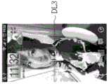
请参考图6A~图6C,图6A~图6C为本发明实施例中一显示画面进行补偿工作的示意图。在本实施例中。图6A为一显示画面的中央处产生一缺陷区域DL1,即对于一NormallyWhite的显示面板来说,缺陷区域DL1是代表该些像素单元为充电不足,相对地,假设对应于一Normally Black的显示面板来说,缺陷区域DL1是代表该些像素单元为过度充电(或者也可表示显示面板上其他位置的像素单元为充电不足)。在此情况下,由于有水平线缺陷的像素单元所显示的显示亮度已高于预定亮度,据此,本实施例将可相应通过上述多种校正与补偿工作,而预先将有水平线缺线的像素单元的灰阶值相应调降(如图6B所示)为一校正区域DL2,进而得到校正与补偿工作后的显示画面(如图6C所示),即该显示画面将包含一正常显示区域DL3,即恢复显示面板102上该些校正区域内一个或多个像素单元的显示亮度为预定亮度。Please refer to FIGS. 6A to 6C . FIGS. 6A to 6C are schematic diagrams of compensation work performed on a display screen according to an embodiment of the present invention. In this example. FIG. 6A shows a defective area DL1 generated in the center of a display screen, that is, for a Normally White display panel, the defective area DL1 represents that the pixel units are insufficiently charged. On the contrary, it is assumed that the display panel corresponds to a Normally Black In other words, the defective area DL1 represents that the pixel units are overcharged (or may also indicate that the pixel units at other positions on the display panel are undercharged). In this case, since the display brightness displayed by the pixel unit with the horizontal line defect has been higher than the predetermined brightness, according to this, this embodiment can correspondingly pass the above-mentioned various correction and compensation work, and pre-define the pixel with the missing horizontal line The grayscale value of the unit is correspondingly lowered (as shown in FIG. 6B ) as a correction area DL2, and then a display image after correction and compensation work (as shown in FIG. 6C ) is obtained, that is, the display image will include a normal display area DL3 , that is, the display brightness of one or more pixel units in the correction regions on the
值得注意地,在其他实施例中,若该些水平线缺陷的像素单元为丛聚模式,且该些像素单元的显示亮度均偏离预定亮度为一固定值时,本实施例的校正与补偿工作将判断其仅包含有一单一缺陷对象,进一步,将对应参考该缺陷对象的一坐标范围,以进行相对应的校正与补偿工作;若该些水平线缺陷的像素单元为分散模式,即判断包含有多个缺陷对象存在时,本实施例也可参考已记录的该些缺陷对象的坐标范围以及该些缺陷对象所包含的缺陷程度,以对应进行该些缺陷对象的校正与补偿工作。请参考图7,图7为本发明实施例中一缺陷显示画面70的示意图,其中缺陷显示画面70包含有多个校正区域且各自对应为不同的缺陷程度。如图7所示,由于缺陷显示画面70已包含多个对应为不同缺陷程度的校正区域,本实施例中的处理器100将对应判断且纪录缺陷显示画面70中多个缺陷对象的相关数据为下表1,以清楚说明该些缺陷对象所对应的坐标范围与缺陷程度,同时,处理器100还可进一步比较不同缺陷程度的像素单元的显示亮度与预定亮度间的差值,以对应判断该些缺陷对象的像素单元所需进行的校正与补偿工作,即对应为不同的方法1~方法3,至于方法1~方法3的详细工作方式,例如可分别为调整不同灰阶值的映像曲线、针对不同色域空间进行亮度补偿工作或进行模拟伽马补偿工作等,然其内容非用以限制本发明的范围。换言之,本实施例可同时针对多个缺陷对象来进行不同类别的校正与补偿工作,以缩短校正流程所需的运行时间与效率,进而配合不同显示设备的设计与应用。It should be noted that, in other embodiments, if the pixel units with horizontal line defects are in the cluster mode, and the display brightness of these pixel units deviates from the predetermined brightness by a fixed value, the correction and compensation work of this embodiment will be It is judged that it only contains a single defect object, and further, a coordinate range of the defect object is correspondingly referenced to perform corresponding correction and compensation work; if the pixel units of these horizontal line defects are in the scattered mode, it is judged that there are multiple When defective objects exist, the present embodiment can also refer to the recorded coordinate ranges of the defective objects and the degree of defects included in the defective objects, so as to perform the corresponding correction and compensation work for the defective objects. Please refer to FIG. 7 . FIG. 7 is a schematic diagram of a
表1Table 1

简言之,本实施例中用于显示设备10的校正方法,可通过侦测模块与目测方式,对应判断显示设备10是否存在需要进行显示亮度的校正与补偿工作的校正区域。若有校正区域存在时,本实施例可相应判断该些校正区域中的一或多个像素单元的缺陷程度、绝对位置与分类数据,以对应进行各类型的数字影像工作及/或模拟伽马补偿工作,直到校正区域内有水平线缺陷的一或多个像素单元的显示亮度恢复为预定亮度且让显示设备10得进行正常的显示工作。当然,本实施例中用于显示设备10的校正方法,也可利用一软件、韧体或硬件等方式来独立呈现,且对应结合其他的电子硬件产品或显示软件工作等,非用以限制本发明的范围。另外,本领域技术人员还可相应地在校正工作进行中,对应加入其他类型的光学影像调整参数或视觉模型调整参数等,来提升显示设备10工作在不同视觉环境的显示性能或应用范围等,也属于本发明的范围。In short, in the calibration method for the
综上所述,本发明实施例提供一种显示设备与校正方法,可针对已出现有水平线缺陷的像素单元来进行校正与补偿工作,以相应调整有水平线缺陷的像素单元的显示亮度。据此,本实施例可通过回收该些水平线缺陷情况不严重的显示设备来降低生产成本,另一方面,本实施例还可提高承载显示设备的电子产品的使用寿命,以对应提高该些电子产品的应用范围与硬件扩充性。To sum up, the embodiments of the present invention provide a display device and a calibration method, which can perform calibration and compensation work for pixel units with horizontal line defects, so as to adjust the display brightness of the pixel units with horizontal line defects accordingly. Accordingly, the present embodiment can reduce the production cost by recycling the display devices with less serious horizontal line defects. On the other hand, the present embodiment can also increase the service life of the electronic product carrying the display device, so as to correspondingly increase the electronic product. Product application range and hardware expandability.
以上所述仅为本发明的优选实施例而已,并不用于限制本发明,对于本领域的技术人员来说,本发明可以有各种更改和变化。凡在本发明的精神和原则之内,所作的任何修改、等同替换、改进等,均应包含在本发明的保护范围之内。The above descriptions are only preferred embodiments of the present invention, and are not intended to limit the present invention. For those skilled in the art, the present invention may have various modifications and changes. Any modification, equivalent replacement, improvement, etc. made within the spirit and principle of the present invention shall be included within the protection scope of the present invention.
Claims (12)
Translated fromChinesePriority Applications (1)
| Application Number | Priority Date | Filing Date | Title |
|---|---|---|---|
| CN201510388863.5ACN106328030B (en) | 2015-07-06 | 2015-07-06 | Calibration method and display device |
Applications Claiming Priority (1)
| Application Number | Priority Date | Filing Date | Title |
|---|---|---|---|
| CN201510388863.5ACN106328030B (en) | 2015-07-06 | 2015-07-06 | Calibration method and display device |
Publications (2)
| Publication Number | Publication Date |
|---|---|
| CN106328030A CN106328030A (en) | 2017-01-11 |
| CN106328030Btrue CN106328030B (en) | 2020-10-30 |
Family
ID=57728152
Family Applications (1)
| Application Number | Title | Priority Date | Filing Date |
|---|---|---|---|
| CN201510388863.5AActiveCN106328030B (en) | 2015-07-06 | 2015-07-06 | Calibration method and display device |
Country Status (1)
| Country | Link |
|---|---|
| CN (1) | CN106328030B (en) |
Families Citing this family (7)
| Publication number | Priority date | Publication date | Assignee | Title |
|---|---|---|---|---|
| CN106847154A (en)* | 2017-02-15 | 2017-06-13 | 京东方科技集团股份有限公司 | Method, device and display device for compensating the bad display panel of display |
| CN107221307A (en) | 2017-07-31 | 2017-09-29 | 京东方科技集团股份有限公司 | The compensation method of display module and compensation device |
| CN107492335A (en)* | 2017-09-26 | 2017-12-19 | 惠科股份有限公司 | Method, structure and restoration system for generating image compensation signal |
| CN107957634B (en)* | 2017-12-06 | 2020-04-17 | 苏州精濑光电有限公司 | Display panel detection method and device |
| KR20230122023A (en)* | 2020-12-29 | 2023-08-22 | 퀄컴 인코포레이티드 | Method and apparatus for adaptive subsampling for demura correction |
| CN115440154A (en)* | 2021-06-01 | 2022-12-06 | 力领科技股份有限公司 | Display panel drive circuit |
| WO2023197241A1 (en)* | 2022-04-14 | 2023-10-19 | 京东方科技集团股份有限公司 | Display defect repairing method for display panel, and display device |
Citations (3)
| Publication number | Priority date | Publication date | Assignee | Title |
|---|---|---|---|---|
| CN102005181A (en)* | 2010-11-19 | 2011-04-06 | 深圳市金立翔光电科技有限公司 | Standard dot matrix light source and image point correction method of LED display screen |
| CN102768816A (en)* | 2012-07-30 | 2012-11-07 | 西安诺瓦电子科技有限公司 | Automatic LED (light-emitting diode) display screen correction method |
| CN103943092A (en)* | 2014-05-05 | 2014-07-23 | 广东威创视讯科技股份有限公司 | Screen color correction method and system for display unit |
Family Cites Families (1)
| Publication number | Priority date | Publication date | Assignee | Title |
|---|---|---|---|---|
| TWI337725B (en)* | 2006-04-10 | 2011-02-21 | Chimei Innolux Corp | Data display method capable of releasing double image and improving mprt |
- 2015
- 2015-07-06CNCN201510388863.5Apatent/CN106328030B/enactiveActive
Patent Citations (3)
| Publication number | Priority date | Publication date | Assignee | Title |
|---|---|---|---|---|
| CN102005181A (en)* | 2010-11-19 | 2011-04-06 | 深圳市金立翔光电科技有限公司 | Standard dot matrix light source and image point correction method of LED display screen |
| CN102768816A (en)* | 2012-07-30 | 2012-11-07 | 西安诺瓦电子科技有限公司 | Automatic LED (light-emitting diode) display screen correction method |
| CN103943092A (en)* | 2014-05-05 | 2014-07-23 | 广东威创视讯科技股份有限公司 | Screen color correction method and system for display unit |
Also Published As
| Publication number | Publication date |
|---|---|
| CN106328030A (en) | 2017-01-11 |
Similar Documents
| Publication | Publication Date | Title |
|---|---|---|
| CN106328030B (en) | Calibration method and display device | |
| US11270663B2 (en) | Method for detecting compensation parameters of brightness, method for compensating brightness, detection device for detecting compensation parameters of brightness, brightness compensation device, display device, and non-volatile storage medium | |
| CN107221290B (en) | mura compensation display method and device and computer readable storage medium | |
| US9892671B2 (en) | Method and device for performing gamma correction for LCD panels | |
| EP3264402A1 (en) | Method for correcting screen asymmetry and device and system thereof | |
| TWI502580B (en) | Systems and methods for mura calibration preparation | |
| US11056078B2 (en) | Multi-screen color correction method and electronic device using the same | |
| US8238640B2 (en) | Display testing apparatus and method | |
| KR20190052195A (en) | Method of compensating for non-uniformity of luminance of a display panel and display device employing the same | |
| CN107945769A (en) | Ambient light intensity detection method and device, storage medium and electronic equipment | |
| US9013580B2 (en) | Method and system for adjusting display parameters | |
| CN106409206A (en) | Display image brightness compensation method and compensation device | |
| CN105825840B (en) | A kind of optical compensation method, optical compensating member and display panel | |
| US10930243B2 (en) | Method and system for adjusting uniformity of image color tones by using a translucent uniformity compensated image layer | |
| CN114331975B (en) | Display screen display defect detection method and device | |
| CN109584792B (en) | Method for quickly adjusting gray scale gamma of O L ED screen | |
| CN115035849A (en) | Gamma debugging method, device, device and storage medium of display panel | |
| TW201523556A (en) | Display device and method for driving same | |
| TWI390483B (en) | Apparatus and method for contrast control | |
| US11334308B2 (en) | Display device and image correction method | |
| US20180261188A1 (en) | Display processing method and apparatus, and display device | |
| CN107195270A (en) | The luminance compensation method and device of display panel | |
| CN114360422A (en) | Afterimage compensation device and display device including the same | |
| CN109686336B (en) | Display device and display control method and device thereof | |
| US10970846B1 (en) | Repairing method for Mura in display panel |
Legal Events
| Date | Code | Title | Description |
|---|---|---|---|
| PB01 | Publication | ||
| PB01 | Publication | ||
| C10 | Entry into substantive examination | ||
| SE01 | Entry into force of request for substantive examination | ||
| GR01 | Patent grant | ||
| GR01 | Patent grant |