CN106325631B - A touch display module with pressure detection and its driving method - Google Patents
A touch display module with pressure detection and its driving methodDownload PDFInfo
- Publication number
- CN106325631B CN106325631BCN201510404705.4ACN201510404705ACN106325631BCN 106325631 BCN106325631 BCN 106325631BCN 201510404705 ACN201510404705 ACN 201510404705ACN 106325631 BCN106325631 BCN 106325631B
- Authority
- CN
- China
- Prior art keywords
- touch
- pressure
- display module
- pulse
- pressure detection
- Prior art date
- Legal status (The legal status is an assumption and is not a legal conclusion. Google has not performed a legal analysis and makes no representation as to the accuracy of the status listed.)
- Expired - Fee Related
Links
Images


Classifications
- G—PHYSICS
- G06—COMPUTING OR CALCULATING; COUNTING
- G06F—ELECTRIC DIGITAL DATA PROCESSING
- G06F3/00—Input arrangements for transferring data to be processed into a form capable of being handled by the computer; Output arrangements for transferring data from processing unit to output unit, e.g. interface arrangements
- G06F3/01—Input arrangements or combined input and output arrangements for interaction between user and computer
- G06F3/03—Arrangements for converting the position or the displacement of a member into a coded form
- G06F3/041—Digitisers, e.g. for touch screens or touch pads, characterised by the transducing means
- G06F3/0412—Digitisers structurally integrated in a display
- G—PHYSICS
- G06—COMPUTING OR CALCULATING; COUNTING
- G06F—ELECTRIC DIGITAL DATA PROCESSING
- G06F3/00—Input arrangements for transferring data to be processed into a form capable of being handled by the computer; Output arrangements for transferring data from processing unit to output unit, e.g. interface arrangements
- G06F3/01—Input arrangements or combined input and output arrangements for interaction between user and computer
- G06F3/03—Arrangements for converting the position or the displacement of a member into a coded form
- G06F3/041—Digitisers, e.g. for touch screens or touch pads, characterised by the transducing means
- G06F3/0414—Digitisers, e.g. for touch screens or touch pads, characterised by the transducing means using force sensing means to determine a position
- G06F3/04144—Digitisers, e.g. for touch screens or touch pads, characterised by the transducing means using force sensing means to determine a position using an array of force sensing means
- G—PHYSICS
- G06—COMPUTING OR CALCULATING; COUNTING
- G06F—ELECTRIC DIGITAL DATA PROCESSING
- G06F3/00—Input arrangements for transferring data to be processed into a form capable of being handled by the computer; Output arrangements for transferring data from processing unit to output unit, e.g. interface arrangements
- G06F3/01—Input arrangements or combined input and output arrangements for interaction between user and computer
- G06F3/03—Arrangements for converting the position or the displacement of a member into a coded form
- G06F3/041—Digitisers, e.g. for touch screens or touch pads, characterised by the transducing means
- G06F3/0416—Control or interface arrangements specially adapted for digitisers
- G06F3/04166—Details of scanning methods, e.g. sampling time, grouping of sub areas or time sharing with display driving
- G—PHYSICS
- G06—COMPUTING OR CALCULATING; COUNTING
- G06F—ELECTRIC DIGITAL DATA PROCESSING
- G06F3/00—Input arrangements for transferring data to be processed into a form capable of being handled by the computer; Output arrangements for transferring data from processing unit to output unit, e.g. interface arrangements
- G06F3/01—Input arrangements or combined input and output arrangements for interaction between user and computer
- G06F3/03—Arrangements for converting the position or the displacement of a member into a coded form
- G06F3/041—Digitisers, e.g. for touch screens or touch pads, characterised by the transducing means
- G06F3/044—Digitisers, e.g. for touch screens or touch pads, characterised by the transducing means by capacitive means
- G06F3/0443—Digitisers, e.g. for touch screens or touch pads, characterised by the transducing means by capacitive means using a single layer of sensing electrodes
- G—PHYSICS
- G06—COMPUTING OR CALCULATING; COUNTING
- G06F—ELECTRIC DIGITAL DATA PROCESSING
- G06F3/00—Input arrangements for transferring data to be processed into a form capable of being handled by the computer; Output arrangements for transferring data from processing unit to output unit, e.g. interface arrangements
- G06F3/01—Input arrangements or combined input and output arrangements for interaction between user and computer
- G06F3/03—Arrangements for converting the position or the displacement of a member into a coded form
- G06F3/041—Digitisers, e.g. for touch screens or touch pads, characterised by the transducing means
- G06F3/044—Digitisers, e.g. for touch screens or touch pads, characterised by the transducing means by capacitive means
- G06F3/0446—Digitisers, e.g. for touch screens or touch pads, characterised by the transducing means by capacitive means using a grid-like structure of electrodes in at least two directions, e.g. using row and column electrodes
- G—PHYSICS
- G06—COMPUTING OR CALCULATING; COUNTING
- G06F—ELECTRIC DIGITAL DATA PROCESSING
- G06F2203/00—Indexing scheme relating to G06F3/00 - G06F3/048
- G06F2203/041—Indexing scheme relating to G06F3/041 - G06F3/045
- G06F2203/04101—2.5D-digitiser, i.e. digitiser detecting the X/Y position of the input means, finger or stylus, also when it does not touch, but is proximate to the digitiser's interaction surface and also measures the distance of the input means within a short range in the Z direction, possibly with a separate measurement setup
Landscapes
- Engineering & Computer Science (AREA)
- General Engineering & Computer Science (AREA)
- Theoretical Computer Science (AREA)
- Human Computer Interaction (AREA)
- Physics & Mathematics (AREA)
- General Physics & Mathematics (AREA)
- Force Measurement Appropriate To Specific Purposes (AREA)
- Position Input By Displaying (AREA)
Abstract
Translated fromChinese
Description
Translated fromChinese【技术领域】【Technical field】
本发明涉及触控领域,尤其涉及一种具有压力侦测的触控显示模组及其驱动方法。The invention relates to the field of touch control, in particular to a touch display module with pressure detection and a driving method thereof.
【背景技术】【Background technique】
随着制程技术的进步,触控显示模组已经成功将触控面板与显示面板进行了整合,使得使用者可直接透过触控面板指示电子装置执行所需的工作。一般来说,触控显示模组上的触控感测单元及像素单元皆以矩阵方式排列于二维平面上,并根据扫描脉冲讯号,决定更新显示画面及侦测触控点的时序。With the advancement of manufacturing technology, the touch display module has successfully integrated the touch panel and the display panel, so that the user can directly instruct the electronic device to perform the required work through the touch panel. Generally speaking, the touch sensing units and pixel units on the touch display module are arranged in a matrix on a two-dimensional plane, and the timing of updating the display screen and detecting touch points is determined according to the scan pulse signal.
一般的平面显示面板而言,其显示画面是由二维的像素所组成,以薄膜晶体管(TFT)的液晶显示(LCD)模组所构成的TFT-LCD显示面板为例来说明。显示面板包括多个阵列的像素单元。如果是彩色显示的话,每一个像素又由三个次像素单元所组成来分显示红绿蓝的颜色。每一个像素单元包括至少一个TFT作为驱动开关。显示面板在驱动机制上包括栅极驱动器与源极驱动器,所述栅极驱动器根据待显讯号产生栅极扫描脉冲以控制像素单元的显示色彩。所述源极驱动器根据待显示讯号产生源极扫描脉冲以控制像素单元的色彩显示强度。For a general flat display panel, its display screen is composed of two-dimensional pixels, and a TFT-LCD display panel composed of a thin film transistor (TFT) liquid crystal display (LCD) module is taken as an example for illustration. The display panel includes a plurality of arrays of pixel units. If it is a color display, each pixel is composed of three sub-pixel units to display red, green and blue colors. Each pixel unit includes at least one TFT as a driving switch. The display panel includes a gate driver and a source driver in a driving mechanism. The gate driver generates a gate scan pulse according to a signal to be displayed to control the display color of the pixel unit. The source driver generates source scan pulses according to the signal to be displayed to control the color display intensity of the pixel unit.
触控面板对应的有触控驱动器,触控驱动器产生触控驱动信号以控制侦测触控点的时序。The touch panel corresponds to a touch driver, and the touch driver generates touch driving signals to control the timing of detecting touch points.
为了进一步丰富触控显示模组的功能,目前已有部分触控面板会加装压力传感器,所述压力传感器包括多个压感单元,该压感单元侦测出使用者的按压力值,其可对应匹配于不同压力值下的设备功能,譬如不同力度下同一触控点可匹配多种功能。这样通过压力传感器的设置进一步为使用者带来了更丰富的体验。现有的触控显示模组设置有对应的有压力驱动器,压力驱动器产生压力驱动扫描脉冲以控制侦测按压力值的时序。In order to further enrich the functions of the touch display module, some touch panels are equipped with pressure sensors. The pressure sensors include a plurality of pressure-sensitive units. It can be matched to the device functions under different pressure values, for example, the same touch point can be matched with multiple functions under different forces. In this way, the setting of the pressure sensor further brings a richer experience to the user. The existing touch display module is provided with a corresponding pressure driver, and the pressure driver generates pressure-driven scan pulses to control the timing of detecting the pressure value.
整合有触控面板和显示面板的触控显示模组虽然功能丰富,但存在一个严重的问题:由于触控显示模组集成度的增加,各元器件以及导电线的排布越来越紧密,电讯号之间的干扰非常严重,以至于触控点位置以及按压力值的侦测精准度降低,如何克服触控面板加载压力传感器,以及触控面板与显示面板在整合时所遇到的讯号之间相互干扰的问题是业界急于解决的一大难题。Although the touch display module integrated with the touch panel and the display panel is rich in functions, there is a serious problem: due to the increase in the integration of the touch display module, the arrangement of components and conductive wires is getting closer and closer. The interference between electrical signals is so serious that the detection accuracy of the position of the touch point and the pressure value is reduced. How to overcome the pressure sensor loaded on the touch panel and the signals encountered during the integration of the touch panel and the display panel The problem of mutual interference between them is a major problem that the industry is eager to solve.
【发明内容】【Content of invention】
为克服目前触控显示模组所存在的电讯号干扰噪声的问题,本发明提供一种抗噪性能好的具有压力侦测的触控显示模组及其驱动方法。In order to overcome the problem of electrical signal interference noise existing in the current touch display module, the present invention provides a touch display module with good noise resistance and pressure detection and a driving method thereof.
本发明提供了一种解决上述技术问题的技术方案:一种具有压力侦测的触控显示模组,包括阵列设置的多个像素单元及三维传感器,该三维传感器包括多个触控单元与至少一压感单元,所述多个像素单元接收一栅极驱动扫描脉冲以控制其显示色彩更新时序;所述多个触控单元接收一触控扫描脉冲以控制侦测触控点的时序;所述至少一压感单元接收一压力扫描脉冲以控制侦测按压力的时序,所述栅极驱动脉冲,所述触控扫描脉冲以及所述压力扫描脉冲之间的电位切换点错开。The present invention provides a technical solution to the above technical problems: a touch display module with pressure detection, including a plurality of pixel units arranged in an array and a three-dimensional sensor, the three-dimensional sensor includes a plurality of touch units and at least A pressure-sensitive unit, the plurality of pixel units receive a gate drive scan pulse to control the timing of their display color update; the plurality of touch units receive a touch scan pulse to control the timing of detecting touch points; The at least one pressure sensing unit receives a pressure scanning pulse to control the timing of detecting the pressing force, and the potential switch points between the gate driving pulse, the touch scanning pulse and the pressure scanning pulse are staggered.
优选地,所述栅极驱动脉冲,所述触控扫描脉冲以及所述压力扫描脉冲分时序交替进行,所述触控扫描脉冲以及所述压力扫描脉冲之脉宽不宽于所述栅极驱动脉冲之脉宽。Preferably, the gate drive pulse, the touch scan pulse and the pressure scan pulse are alternately performed in time sequence, and the pulse width of the touch scan pulse and the pressure scan pulse is not wider than that of the gate drive The pulse width of the pulse.
优选地,所述触控扫描脉冲以及所述压力扫描脉冲均与所述栅极扫描脉冲同时序进行。Preferably, both the touch scan pulse and the pressure scan pulse are performed at the same time as the gate scan pulse.
优选地,所述触控扫描脉冲以及所述压力扫描脉冲分时序进行或同时序进行。Preferably, the touch scanning pulse and the pressure scanning pulse are performed in a time sequence or simultaneously.
优选地,所述具有压力侦测的触控显示模组进一步包括至少一屏蔽层,所述多个像素单元位于该屏蔽层的一侧,所述多个触控单元和所述至少一压感单元位于该屏蔽层的另一侧。Preferably, the touch display module with pressure detection further includes at least one shielding layer, the plurality of pixel units are located on one side of the shielding layer, the plurality of touch units and the at least one pressure-sensitive The unit is on the other side of this shield.
优选地,所述多个触控单元和所述至少一压感单元之间设置一屏蔽层。Preferably, a shielding layer is provided between the plurality of touch-sensitive units and the at least one pressure-sensitive unit.
优选地,所述触控显示模组进一步包括设置有至少一所述压感单元的第一压力层和设置有至少一所述压感单元的第二压力层。Preferably, the touch display module further includes a first pressure layer provided with at least one pressure-sensitive unit and a second pressure layer provided with at least one pressure-sensitive unit.
优选地,所述第一压力层之压感单元接收到的压力扫描脉冲,所述第二压力层之压感单元所接收到的压力扫描脉冲以及所述触控单元所接收到的触控扫描脉冲分时序进行或同时序进行。Preferably, the pressure scanning pulse received by the pressure sensing unit of the first pressure layer, the pressure scanning pulse received by the pressure sensing unit of the second pressure layer and the touch scanning received by the touch unit The pulses are performed sequentially or simultaneously.
优选地,所述栅极驱动脉冲,所述触控扫描脉冲以及所述压力扫描脉冲由同一驱动器直接或间接提供。Preferably, the gate drive pulse, the touch scan pulse and the pressure scan pulse are directly or indirectly provided by the same driver.
优选地,所述至少一压感单元为多个压感单元,所述多个压感单元对应内阻为RF0,RF1,RF2······RFn,在所述的压感单元附近设置有与其一一匹配的电阻RC0,RC1,RC2······RCn,RF1,RF2······RFn与RC0,RC1,RC2······RCn互为参考电阻,所述具有压力侦测的触控显示模组进一步包括一压力信号处理器,该压力信号处理器包括一电阻Ra,一电阻Rb,多路复用器MUX1与多路复用器MUX2,RF0,RF1,RF2······RFn接入多路复用器MUX1的输入端,RC0,RC1,RC2······RCn接入所述多路复用器MUX2的输入端,所述多路复用器MUX1与MUX2分别选择相匹配的电阻RFn和RCn输出并与电阻Ra和Rb构成惠斯通电桥,所述RF0,RF1,RF2······RFn阻值变化量与其所受到的按压力值相关联;请注意,于本发明中电阻Ra和Rb属于电桥中固定共用的电阻,又称共用电阻。Preferably, the at least one pressure-sensing unit is a plurality of pressure-sensing units, and the corresponding internal resistances of the plurality of pressure-sensing units are RF0, RF1, RF2...RFn, and are arranged near the pressure-sensing unit There are resistors RC0, RC1, RC2 that match one by one...RCn, RF1, RF2...RFn and RC0, RC1, RC2...RCn are mutual reference resistors, the The touch display module with pressure detection further includes a pressure signal processor, the pressure signal processor includes a resistor Ra, a resistor Rb, multiplexer MUX1 and multiplexer MUX2, RF0, RF1, RF2·······RFn is connected to the input end of the multiplexer MUX1, RC0, RC1, RC2·······RCn is connected to the input end of the multiplexer MUX2, the multiplexer Multiplexers MUX1 and MUX2 respectively select matching resistors RFn and RCn to output and form a Wheatstone bridge with resistors Ra and Rb. The RF0, RF1, RF2······. The pressure values are related; please note that in the present invention, the resistors Ra and Rb are fixed and shared resistors in the bridge, also known as shared resistors.
优选地,所述具有压力侦测的触控显示模组进一步包括参考电阻与共用电阻,参考电阻与共用电阻以及所述至少一压感单元构成的一惠斯通电桥,所述惠斯通电桥输出端电连接有一运算放大电路,所述运算放大电路输出端依次电连接有滤波电路和ADC电路。Preferably, the touch display module with pressure detection further includes a reference resistor and a shared resistor, a Wheatstone bridge formed by the reference resistor, the shared resistor and the at least one pressure sensing unit, and the Wheatstone bridge The output end is electrically connected with an operational amplifier circuit, and the output end of the operational amplifier circuit is electrically connected with a filter circuit and an ADC circuit in turn.
优选地,所述具有压力侦测的触控显示模组进一步包括一触控信号接收模组,一压力信号接收模组以及一集成处理器,所触控单元电连接于所述触控信号接收模组,所述至少一压感单元电连接于所述压力信号接收模组,所述触控信号接收模组与所述压力信号接收模组电连接于所述集成处理器。Preferably, the touch display module with pressure detection further includes a touch signal receiving module, a pressure signal receiving module and an integrated processor, the touch unit is electrically connected to the touch signal receiving module module, the at least one pressure sensing unit is electrically connected to the pressure signal receiving module, and the touch signal receiving module and the pressure signal receiving module are electrically connected to the integrated processor.
优选地,所述触控单元由多条第一方向触控电极与多条第二方向触控电极所界定。Preferably, the touch unit is defined by a plurality of touch electrodes in the first direction and a plurality of touch electrodes in the second direction.
优选地,所述多条第一方向触控电极相互平行,所述多条第二方向触控电极相互平行,所述多条第一方向触控电极与所述多条第二方向触控电极以及至少一压感单元设置在同一平面内,所述多条第一方向触控电极与所述多条第二方向触控电极之间呈一定夹角,在所述多条第一方向触控电极之间设置有非触控区,所述至少一压感单元设置在该非触控区内,所述至少一压感单元,所述多条第一方向触控电极与所述多条第二方向触控电极之间有交叠区域,在所述交叠区域内设置有位于所述多条第一方向触控电极与所述多条第二方向触控电极之间的绝缘块。Preferably, the plurality of touch electrodes in the first direction are parallel to each other, the plurality of touch electrodes in the second direction are parallel to each other, and the plurality of touch electrodes in the first direction and the plurality of touch electrodes in the second direction And at least one pressure-sensitive unit is arranged in the same plane, the plurality of first-direction touch electrodes and the plurality of second-direction touch electrodes form a certain angle, and the plurality of first-direction touch electrodes A non-touch area is arranged between the electrodes, the at least one pressure-sensitive unit is arranged in the non-touch area, the at least one pressure-sensitive unit, the plurality of touch electrodes in the first direction and the plurality of first-direction touch electrodes There is an overlapping area between the touch electrodes in the two directions, and an insulating block between the plurality of touch electrodes in the first direction and the touch electrodes in the second direction is arranged in the overlapping area.
优选地,所述多条第一方向触控电极与所述多条第二方向触控电极与压感单元设置在同一平面内,所述多条第一方向触控电极与所述多条第二方向触控电极之间无交叠区域,所述多条第一方向触控电极之间,或所述多条第二方向触控电极之间,或所述多条第一方向触控电极与所述多条第二方向触控电极之间设置有非触控区域,所述至少一压感单元设置在该非触控区内。Preferably, the plurality of touch electrodes in the first direction and the plurality of touch electrodes in the second direction are arranged in the same plane as the pressure-sensitive unit, and the plurality of touch electrodes in the first direction and the plurality of touch electrodes in the second direction There is no overlapping area between the two-direction touch electrodes, between the plurality of first-direction touch electrodes, or between the plurality of second-direction touch electrodes, or between the plurality of first-direction touch electrodes A non-touch area is disposed between the plurality of second-direction touch electrodes, and the at least one pressure-sensitive unit is disposed in the non-touch area.
优选地,所述多条第一方向触控电极相互平行,所述多条第二方向触控电极相互平行,所述多条第一方向触控电极与所述多条第二方向触控电极位于不同的基材层上或设置在同一基材层的不同平面内,在所述多条第一方向触控电极之间有非触控区域,所述至少一压感单元设置在所述非触控区内。Preferably, the plurality of touch electrodes in the first direction are parallel to each other, the plurality of touch electrodes in the second direction are parallel to each other, and the plurality of touch electrodes in the first direction and the plurality of touch electrodes in the second direction Located on different substrate layers or arranged in different planes of the same substrate layer, there is a non-touch area between the plurality of first-direction touch electrodes, and the at least one pressure-sensitive unit is arranged on the non-touch area. within the touch area.
优选地,具有压力侦测的触控显示模组进一步包括一盖板与一触控显示面板,所述触控显示面板包括从上至下依次设置的上偏光片,一上基板,一液晶层,一下基板和一下偏光片,所述多条第一方向触控电极和所述多条第二方向触控电极设置在所述上偏光片下表面,所述上基板上表面或下表面,所述下基板上表面或下表面,所述下偏光片下表面中的一个或两个表面上。Preferably, the touch display module with pressure detection further includes a cover plate and a touch display panel, and the touch display panel includes an upper polarizer, an upper substrate, and a liquid crystal layer sequentially arranged from top to bottom , the lower substrate and the lower polarizer, the plurality of touch electrodes in the first direction and the plurality of touch electrodes in the second direction are arranged on the lower surface of the upper polarizer, and the upper or lower surface of the upper substrate, so The upper surface or the lower surface of the lower substrate, and one or both of the lower surfaces of the lower polarizer.
优选地,所述至少一压感单元与所述多条第一方向触控电极和/或所述多条第二方向触控电极互补。Preferably, the at least one pressure sensitive unit is complementary to the plurality of touch electrodes in the first direction and/or the plurality of touch electrodes in the second direction.
本发明还提供一种具有压力侦测触控显示模组之驱动方法,所述具有压力侦测触控显示模组包括阵列设置的多个像素单元及一三维传感器,所述三维传感器包括多个触控单元与至少二压感单元,所述驱动方法包括步骤:S1:提供一栅极驱动扫描脉冲至所述像素单元以控制其显示色彩更新时序;S2:提供一触控扫描脉冲至所述触控单元以控制侦测触控点的时序;及S3:提供一压力扫描脉冲至所述压感单元以控制侦测按压力的时序;其中,所述栅极驱动脉冲,所述触控扫描脉冲以及所述压力扫描脉冲之间的电位切换点错开。The present invention also provides a driving method for a touch display module with pressure detection, the touch display module with pressure detection includes a plurality of pixel units arranged in an array and a three-dimensional sensor, and the three-dimensional sensor includes a plurality of The touch unit and at least two pressure-sensitive units, the driving method includes steps: S1: provide a gate drive scan pulse to the pixel unit to control its display color update timing; S2: provide a touch scan pulse to the The touch unit is used to control the timing of detecting the touch point; and S3: providing a pressure scanning pulse to the pressure sensing unit to control the timing of detecting the pressing force; wherein, the gate driving pulse, the touch scanning The potential switching points between the pulses and the pressure scan pulses are staggered.
与现有技术相比,本发明所提供的具有压力侦测的触控显示模组具有如下优点:Compared with the prior art, the touch display module with pressure detection provided by the present invention has the following advantages:
1.由于电容式触控面板采用的是人体感应电流的原理进行触控点侦测的,而当触控电极与压力侦测电极设置在同一基材层上且显示面板靠近触控面板时,元器件和导电线等之间的排布非常密切,讯号之间的相互干扰非常严重而导致触控点位置侦测及按压力值侦测不精准。本发明中巧妙的通过选择电路和/或脉冲重整电路将为像素单元提供栅极驱动扫描脉冲的栅极驱动器加以利用,通过选择电路和/或脉冲重整电路进行选择,位移,脉宽缩窄以及分频等处理后提供压力扫描脉冲与触控扫描脉冲。栅极扫描脉冲,压力扫描脉冲与触控扫描脉冲之间可以分时序或同时序进行。同时序时,栅极扫描脉冲,压力扫描脉冲与触控扫描脉冲中的两者或三者同时进行,但它们之间的电位切换点相互错位(在电位切换点处,讯号极易受到外部干扰而导致电信号不稳定,讯号错位等等),这样使得具有压力侦测的触控显示模组反应速度快,讯号之间的干扰降低,触控稳定性较好。在分时序时,栅极扫描脉冲,压力扫描脉冲与触控扫描脉冲分时段进行,故,电讯号之间的干扰也同样降低,具有压力侦测的触控显示模组的触控稳定性得到大幅的提升。1. Since the capacitive touch panel uses the principle of human body induction current to detect the touch point, when the touch electrode and the pressure detection electrode are arranged on the same substrate layer and the display panel is close to the touch panel, The arrangement of components and conductive wires is very close, and the mutual interference between signals is very serious, which leads to inaccurate detection of touch point position and pressure value. In the present invention, through the selection circuit and/or the pulse reforming circuit, the gate driver that provides the gate drive scanning pulse for the pixel unit is utilized, and the selection, displacement, and pulse width reduction are performed through the selection circuit and/or the pulse reforming circuit. After processing such as narrowing and frequency division, pressure scanning pulses and touch scanning pulses are provided. The gate scan pulses, the pressure scan pulses and the touch scan pulses can be sequentially or simultaneously performed. At the same time, two or three of the gate scan pulse, pressure scan pulse and touch scan pulse are performed at the same time, but the potential switching points between them are misplaced (at the potential switching point, the signal is extremely susceptible to external interference resulting in unstable electrical signals, signal misalignment, etc.), so that the touch display module with pressure detection has a fast response speed, the interference between signals is reduced, and the touch stability is better. When the timing is divided, the grid scan pulse, the pressure scan pulse and the touch scan pulse are divided into periods, so the interference between electrical signals is also reduced, and the touch stability of the touch display module with pressure detection is improved. Substantial improvement.
2.至少一屏蔽层位于所述多个像素单元与多个触控单元之间,和/或所述至少一压感单元之间与触控单元之间,所述屏蔽层可以有效地降低触控面板与显示面板之间、触控单元与压力单元之间的相互讯号干扰。2. At least one shielding layer is located between the plurality of pixel units and the plurality of touch units, and/or between the at least one pressure-sensitive unit and the touch unit, and the shielding layer can effectively reduce the touch Mutual signal interference between the control panel and the display panel, between the touch unit and the pressure unit.
3.该具有压力侦测的触控显示模组在进行显示的同时,其不仅能够侦测触控点位置,而且能够侦测到触控点的压力值。触控传感器与压力传感器的通过同一栅极驱动器来驱动,其节约了硬件成本,简化了电路设计,提升了具有压力侦测的触控显示模组的集成度,且从一定程度上降低了具有压力侦测的触控显示模组的厚度与重量。触控传感器与压力传感器以及显示面板的导电线结构上靠近,现有技术中采用不同的驱动器分别对像素单元,触控单元与压感单元进行驱动,其设计空间相比较小,元器件的排布密切不利于散热,本发明则很好地解决了这个问题。3. The touch display module with pressure detection can not only detect the position of the touch point, but also detect the pressure value of the touch point while displaying. The touch sensor and the pressure sensor are driven by the same gate driver, which saves hardware cost, simplifies the circuit design, improves the integration of the touch display module with pressure detection, and reduces the power consumption of the touch display module to a certain extent. The thickness and weight of the pressure detection touch display module. The touch sensor is structurally close to the pressure sensor and the conductive lines of the display panel. In the prior art, different drivers are used to drive the pixel unit, the touch unit and the pressure-sensing unit respectively. The design space is relatively small, and the arrangement of components is relatively small. Close cloth is not conducive to heat dissipation, and the present invention solves this problem well.
4.本发明中采用惠斯通电桥对按压力值进行侦测,其电路结构简单,控制精度高。最重要的所述压力信号处理器中采用电桥与多路复用器结合,通过多路复用器选择不同的压感单元,但不同压感单元在侦测压力信号时所构成的惠斯通电桥中,电阻Ra与Rb为共享电阻,这样设计可以大大地降低惠斯通电桥中的电阻数量,且不同压感单元在进行压力侦测时,由于其部分硬件共享,故相互之间的误差率降低。更进一步,所述压感单元所对应的内阻RF0,RF1,RF2······RFn一一对应设置有RC0,RC1,RC2······RCn互为参考电阻,该参考电阻设置在RF0,RF1,RF2······RFn附近,这样,它们之间的受到温度影响一致,受到的其他噪声也近似,这样有利于惠斯通电桥的稳定,降低了硬件电路因自身温度漂移,环境因素所带来的信号误判。RF0,RF1,RF2······RFn与RC0,RC1,RC2······RCn互为参考电阻,这样降低噪声的同时优化了资源的配置。惠斯通电桥的输出信号端接有运算放大电路,所述运算放大电路不仅可以将输出信号U0进行放大,且其可以利用运算放大电路抑制噪声的特性来降低噪声。以RF0与RC0为例来进行说明,在上基板受到按压力时,RF0电阻值变化为△r,但实际上RF0受到如温度以及其他干扰而会产生△s的噪声,对于参考电阻RC0来说,其受到如温度以及其他干扰与其附近的RF0一致,大小也为△s的噪声,该噪声△s在运算放大电路的反向输入端经过反向后即与同向输入端的压敏电阻RF0的噪声相抵消,这样,大大的降低的其他噪声所带来的干扰,进一步提升了压力信号的侦测精度。4. In the present invention, a Wheatstone bridge is used to detect the pressure value, and the circuit structure is simple and the control precision is high. The most important said pressure signal processor adopts the combination of electric bridge and multiplexer, and selects different pressure-sensitive units through multiplexer, but different pressure-sensitive units form Wheath when detecting the pressure signal. In the current bridge, the resistors Ra and Rb are shared resistors. This design can greatly reduce the number of resistors in the Wheatstone bridge, and when different pressure sensing units perform pressure detection, because part of their hardware is shared, the mutual interaction The error rate is reduced. Furthermore, the internal resistances RF0, RF1, RF2...RFn corresponding to the pressure sensing unit are provided with RC0, RC1, RC2...RCn are mutually reference resistors, and the reference resistors Set it near RF0, RF1, RF2······RFn, so that they are affected by the same temperature, and the other noises are also similar, which is conducive to the stability of the Wheatstone bridge and reduces the hardware circuit due to its own Signal misjudgment caused by temperature drift and environmental factors. RF0, RF1, RF2·······RFn and RC0, RC1, RC2·······RCn are mutual reference resistors, which reduces noise and optimizes resource allocation. The output signal of the Wheatstone bridge is connected with an operational amplifier circuit, and the operational amplifier circuit can not only amplify the output signal U0, but also reduce noise by using the noise suppression characteristic of the operational amplifier circuit. Taking RF0 and RC0 as an example, when the upper substrate is pressed, the resistance value of RF0 changes to △r, but in fact, RF0 will generate △s noise due to temperature and other disturbances. For the reference resistor RC0 , it is subject to such as temperature and other disturbances that are consistent with RF0 nearby, and the noise is also △s. The noise is offset, so that the interference caused by other noises is greatly reduced, and the detection accuracy of the pressure signal is further improved.
5.本实施例中,在触控电极的非触控区设置压感单元,其通过绝缘块的设置可以将压感单元以及触控电极集成在同一平面,这样大大的降低了具有压力侦测的触控显示模组的厚度,尤其是触控电极与压感单元之间互补设置,可以使具有压力侦测的触控显示模组的显示效果更佳。5. In this embodiment, the pressure-sensitive unit is set in the non-touch area of the touch electrode, and the pressure-sensitive unit and the touch electrode can be integrated on the same plane through the setting of the insulating block, which greatly reduces the need for pressure detection. The thickness of the touch display module, especially the complementary arrangement between the touch electrodes and the pressure-sensitive unit, can make the display effect of the touch display module with pressure detection better.
【附图说明】【Description of drawings】
图1A是本发明第一实施例具有压力侦测的触控显示模组的层状结构示意图。FIG. 1A is a schematic diagram of a layered structure of a touch display module with pressure detection according to a first embodiment of the present invention.
图1B是本发明第一实施例具有压力侦测的触控显示模组的层状结构之变形一的示意图。1B is a schematic diagram of
图1C是本发明第一实施例具有压力侦测的触控显示模组的层状结构之变形二的示意图。1C is a schematic diagram of
图1D是本发明第一实施例具有压力侦测的触控显示模组的层状结构之变形三的示意图。1D is a schematic diagram of
图2是本发明第一实施例具有压力侦测的触控显示模组之电极图案层的平面结构示意图。2 is a schematic plan view of the electrode pattern layer of the touch display module with pressure detection according to the first embodiment of the present invention.
图3是图2中A处的放大结构示意图。FIG. 3 is a schematic diagram of an enlarged structure at point A in FIG. 2 .
图4A是本发明第一实施例具有压力侦测的触控显示模组的电路结构模块示意图。FIG. 4A is a schematic diagram of a circuit structure module of the touch display module with pressure detection according to the first embodiment of the present invention.
图4B是本发明第一实施例具有压力侦测的触控显示模组的电路结构模块的变形结构示意图。4B is a schematic diagram of a modified structure of the circuit structure module of the touch display module with pressure detection according to the first embodiment of the present invention.
图5A是本发明第一实施例具有压力侦测的触控显示模组的立体结构示意图。FIG. 5A is a schematic perspective view of the three-dimensional structure of the touch display module with pressure detection according to the first embodiment of the present invention.
图5B是本发明第一实施例具有压力侦测的触控显示模组的立体结构变形示意图。5B is a schematic deformation diagram of the three-dimensional structure of the touch display module with pressure detection according to the first embodiment of the present invention.
图6是本发明第一实施例具有压力侦测的触控显示模组之触控扫描脉冲与压力扫描脉冲以及栅极扫描脉冲的时序图。6 is a timing diagram of touch scan pulses, pressure scan pulses, and gate scan pulses of the touch display module with pressure detection according to the first embodiment of the present invention.
图7是图4A中压力信号处理器的电路结构示意图。Fig. 7 is a schematic diagram of the circuit structure of the pressure signal processor in Fig. 4A.
图8A是图7中压力信号侦测原理图。FIG. 8A is a schematic diagram of the pressure signal detection in FIG. 7 .
图8B是图7中另一压力信号侦测原理图。FIG. 8B is another principle diagram of pressure signal detection in FIG. 7 .
图9是本发明第二实施例具有压力侦测的触控显示模组之触控扫描脉冲与压力扫描脉冲以及栅极扫描脉冲的时序图。9 is a timing diagram of touch scan pulses, pressure scan pulses, and gate scan pulses of the touch display module with pressure detection according to the second embodiment of the present invention.
图10是本发明第三实施例具有压力侦测的触控显示模组之触控扫描脉冲与压力扫描脉冲以及栅极扫描脉冲的时序图。10 is a timing diagram of touch scan pulses, pressure scan pulses, and gate scan pulses of the touch display module with pressure detection according to the third embodiment of the present invention.
图11a以及图11b是本发明第四实施例具有压力侦测的触控显示模组之触控扫描脉冲与压力扫描脉冲以及栅极扫描脉冲的时序图。11a and 11b are timing diagrams of touch scan pulses, pressure scan pulses and gate scan pulses of the touch display module with pressure detection according to the fourth embodiment of the present invention.
图12是本发明第五实施例具有压力侦测的触控显示模组之触控扫描脉冲与压力扫描脉冲以及栅极扫描脉冲的时序图。12 is a timing diagram of touch scan pulses, pressure scan pulses, and gate scan pulses of the touch display module with pressure detection according to the fifth embodiment of the present invention.
图13是本发明第六实施例具有压力侦测的触控显示模组的电路结构模块示意图。FIG. 13 is a schematic block diagram of a circuit structure of a touch display module with pressure detection according to a sixth embodiment of the present invention.
图14是本发明第六实施例具有压力侦测的触控显示模组之触控扫描脉冲与压力扫描脉冲以及栅极扫描脉冲的时序图。14 is a timing diagram of touch scan pulses, pressure scan pulses, and gate scan pulses of the touch display module with pressure detection according to the sixth embodiment of the present invention.
图15是本发明第七实施例具有压力侦测的触控显示模组之电极图案层的平面结构示意图。15 is a schematic plan view of the electrode pattern layer of the touch display module with pressure detection according to the seventh embodiment of the present invention.
图16A是本发明第八实施例具有压力侦测的触控显示模组的层状结构示意图。16A is a schematic diagram of the layered structure of the touch display module with pressure detection according to the eighth embodiment of the present invention.
图16B是图16A中电极图案层的平面结构示意图。FIG. 16B is a schematic plan view of the electrode pattern layer in FIG. 16A .
图17是本发明第九实施例具有压力侦测的触控显示模组的层状结构的示意图。FIG. 17 is a schematic diagram of the layered structure of the touch display module with pressure detection according to the ninth embodiment of the present invention.
图18A是本发明第九实施例具有压力侦测的触控显示模组的层状结构变形一的示意图。FIG. 18A is a schematic diagram of a
图18B是本发明第九实施例具有压力侦测的触控显示模组的层状结构变形二的示意图。FIG. 18B is a schematic diagram of a second layered structure variation of the touch display module with pressure detection according to the ninth embodiment of the present invention.
图19是本发明第九实施例具有压力侦测的触控显示模组中第一压力层与第二压力层的局部叠加效果示意图。19 is a schematic diagram of partial superimposition effects of the first pressure layer and the second pressure layer in the touch display module with pressure detection according to the ninth embodiment of the present invention.
图20是本发明第九实施例具有压力侦测的触控显示模组之触控扫描脉冲与压力扫描脉冲以及栅极扫描脉冲的时序图。20 is a timing diagram of touch scan pulses, pressure scan pulses, and gate scan pulses of the touch display module with pressure detection according to the ninth embodiment of the present invention.
图21是本发明第十实施例具有压力侦测的触控显示模组之触控扫描脉冲与压力扫描脉冲以及栅极扫描脉冲的时序图。21 is a timing diagram of touch scan pulses, pressure scan pulses and gate scan pulses of the touch display module with pressure detection according to the tenth embodiment of the present invention.
图22是本发明第十一实施例具有压力侦测的触控显示模组之触控扫描脉冲与压力扫描脉冲以及栅极扫描脉冲的时序图。22 is a timing diagram of touch scan pulses, pressure scan pulses, and gate scan pulses of the touch display module with pressure detection according to the eleventh embodiment of the present invention.
图23是本发明第十二实施例具有压力侦测的触控显示模组的层状结构示意图。23 is a schematic diagram of the layered structure of the touch display module with pressure detection according to the twelfth embodiment of the present invention.
【具体实施方式】【Detailed ways】
为了使本发明的目的,技术方案及优点更加清楚明白,以下结合附图及实施实例,对本发明进行进一步详细说明。应当理解,此处所描述的具体实施例仅仅用以解释本发明,并不用于限定本发明。In order to make the purpose, technical solutions and advantages of the present invention more clear, the present invention will be further described in detail below in conjunction with the accompanying drawings and implementation examples. It should be understood that the specific embodiments described here are only used to explain the present invention, not to limit the present invention.
请参阅图1A,本发明第一实施例具有压力侦测的触控显示模组10从上至下(本发明中所涉及的上、下左右等位置词仅限于指定视图中的相对位置,而非绝对位置)包括一触控面板8,一显示面板9以及信号处理电路15,该触控面板8与显示面板9均通过导电线与信号处理电路电连接。Please refer to FIG. 1A , the first embodiment of the present invention has a
触控面板8从上至下包括一上基板11,一贴合层12,一三维传感器13以及一基材层14,所述三维传感器13与信号处理电路15之间通过导电线(图未视)电连接。The touch panel 8 includes an upper substrate 11 from top to bottom, a
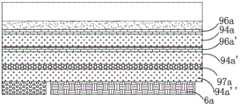
所述具有压力侦测的触控显示模组10还可以进一步选择性地包括至少一屏蔽层,增加至少一屏蔽层时,具有压力侦测的触控显示模组10的层状结构之变型如图1B、1C、与1D所示:The
如图1B,在触控面板8a与显示面板9a之间设置了一屏蔽层7a,该屏蔽层7a为一金属层,其可以以降低触控面板8a与显示面板9a之间的讯号互扰。As shown in FIG. 1B , a
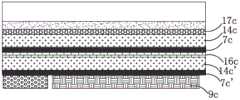
如图1C,所述三维传感器(未标号)包括压力传感器16c与触控传感器17c,所述触控传感器17c与压力传感器16c分别设置在第一基材层14c与第二基材层上14c’上。在所述压力传感器16c与触控传感器17c之间设置有一第一屏蔽层7c,在所述压力传感器16c与显示面板9c之间设置有第二屏蔽层7c’,这样,第一屏蔽层7c与第二屏蔽层7c’可以有效地把压力传感器16c与触控传感器17c以及显示面板9c之间的讯号互扰降低。实际上,我们可以选择仅设置第一屏蔽层7c或第二屏蔽层7c’。压力传感器16c与触控传感器17c位置可以进行互换。As shown in FIG. 1C, the three-dimensional sensor (not labeled) includes a
如图1D,所述三维传感器(未标号)包括压力传感器16d与触控传感器(图未视),所述触控传感器集成于显示面板9d(in-cell结构或者on-cell结构)内,所述压力传感器16d所在平面的上方及下方分别设置有一第一屏蔽层7d与第二屏蔽层7d’,这样,第一屏蔽层7d与第二屏蔽层7d’可以有效地把压力传感器16d与集成有触控传感器的显示面板9d之间的讯号互扰降低。实际上,我们可以选择仅设置第一屏蔽层7d或第二屏蔽层7d’。As shown in FIG. 1D, the three-dimensional sensor (not labeled) includes a
图1A中所示的上基板11可以认定为我们传统触控面板上的触摸盖板,所谓的盖板包括一触控操作面与一组件安装面,其触控操作面用于手指或触控笔等进行触控操作,组件安装面则用于安装触控电极组件或显示面板等。The upper substrate 11 shown in FIG. 1A can be identified as a touch cover on our traditional touch panel. The so-called cover includes a touch operation surface and a component mounting surface. The touch operation surface is used for fingers or touch touch operation with a pen, etc., and the component mounting surface is used for mounting touch electrode components or display panels, etc.
贴合层12可以选用OCA(光学透明胶,Optical Clear Adhesive)或LOCA(液态光学透明胶,Liquid Optical Clear Adhesive)。The
基材层14的材质可以是柔性基材,也可以是刚性基材,基材层14作为三维传感器13的承载层,其通过贴合层12贴合于上基板11的下表面;须留意,以柔性基材作为承载层有助于三维传感器13有更好的压力感测效果。The material of the
所述信号处理电路15设置在基材层14的下方,其位置不作限定,其也可以设置于基材层14上方或其一侧或其它适合的地方。The
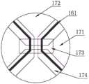
请参阅图2与图3,三维传感器13包括压力传感器16与触控传感器17,两者可以是共平面结构(即如图2与图3所示)或分离结构(即如图18A所示),该压力传感器16包括至少一压感单元161。触控传感器17包括触控电极:设置在X方向上的多条相互平行的第一方向触控电极171,以及在Y方向上的多条相互平行的第二方向触控电极172(图2中分别以4条第一方向触控电极171、4条第二方向触控电极172以及4个压感单元161为例来进行示意说明,实际上,数量不作限制,且压感单元161的数量也可以少于,等于或多于第一触控电极171或第二触控电极172的数量,于变型实施实例中每一条压感单元161可以包含至少两条并排紧靠的回路,达到数量加倍且压感加成的效果)。在本实施例中,所述X方向与Y方向正交,但X和Y方向的夹角角度不作限定。所述多条第一方向触控电极171与多条第二方向触控电极172正交,在两者的交叠区域处,第一方向触控电极171与第二方向触控电极172之间设置有绝缘块173。除交叠区域外,多条第一方向触控电极172之间设置有非触控区174,所述的压感单元161设在该非触控区174内,绝缘块173在压感单元161与第二方向触控电极172之间的交叠区域同样存在,即所述绝缘块173将第一方向触控电极171、第二方向触控电极172以及压感单元161之间的相互交叠的区域覆盖,以使得第一方向触控电极171、第二方向触控电极172以及压感单元161之间相互电性绝缘。最佳地,所述压感单元161的形状与第一方向触控电极171以及第二方向触控电极172形状互补。压感单元161、第一方向触控电极171以及第二方向触控电极172材质可以是ITO或金属导电线或纳米银线导电层。于本实施例中,若压感单元161、第一方向触控电极171以及第二方向触控电极172皆采用ITO制程,将有助于简化制程设计。Please refer to FIGS. 2 and 3 , the three-
多个触控点在X及Y方向上的坐标位置分别由第一方向触控电极171与第二方向触控电极172来确定,而与两方向触控电极交错的压感单元161则负责力度侦测。The coordinate positions of multiple touch points in the X and Y directions are respectively determined by the first-
显示面板9包括一像素阵列(未标号),该像素阵列包括多个阵列的像素单元91(标号见图5A及5B),每一像素单元91根据待显示讯号来控制其显示效果,所述显示效果的控制包括显示色彩控制以及色彩显示强度的控制。The
请参阅图4A与图5A,信号处理电路15包括一三维控制器18与一压力信号处理器19,压力信号处理器19与三维控制器18电性连接。压力传感器16电性连接于三维控制器18与压力信号处理器19。触控传感器17电性连接于三维控制器18。Please refer to FIG. 4A and FIG. 5A , the
压力信号处理器19将压力传感器16所传输过来的压力信号进行处理,其包括一电桥191与一多路复用器192,该多路复用器192电性连接于电桥191。The
三维控制器18包括一栅极驱动器181a,一源极驱动器181b,一驱动脉冲处理电路187,一触控信号接收模组182,一压力信号接收模组183以及一集成处理器186,栅极处理器181a根据待显示讯号产生栅极扫描脉冲Vg_1~Vg_n以指示像素单元91的显示色彩更新时序,源极处理器181b根据待显示讯号产生源极扫描脉冲Vs_1~Vs_m以指示像素单元91的色彩显示强度。所述驱动脉冲处理电路187包括一选择电路184,一脉冲重整电路185,选择电路184与脉冲重整电路185用于对栅极驱动器18所输出的栅极扫描脉冲Vg_1~Vg_n进行处理。栅极扫描脉冲Vg_1~Vg_n经过选择电路184以及脉冲重整电路185为压力传感器16提供压力扫描脉冲Vf_1~Vf_k以控制侦测压感单元161的时序,并且还为触控传感器17提供触控扫描脉冲Vt_1~Vt_p以控制侦测触控点的时序。The three-
于实务操作上,配合触控传感器17与压力传感器16的传感器特性及需要,选择电路184与脉冲重整电路185用于对栅极驱动器18所输出的栅极扫描脉冲Vg_1~Vg_n进行处理后,可以产生不同于栅极扫描脉冲的脉宽宽度与方波振幅,藉以达到提供因各别传感器需求而适合的脉冲讯号;于本发明中,方波为常见的触控显示模块处理讯号形式,但并不以此为限而可以是任何适合的波型讯号。In practice, in accordance with the sensor characteristics and requirements of the
压力传感器16侦测到压力信号后将该电信号传输至压力信号处理器19,所述压力信号处理器19对该压力信号进行处理后再将其传输给控制器18中的压力信号接收模组183。触控传感器17侦测到触控信号后将该信号传递给触控信号接收模组182。集成处理器186对触控信号接收模组182与压力信号接收模组183的电信号进行运算等处理。After the
选择电路184可以从栅极扫描脉冲Vg_1~Vg_n中选择部分信号进行输出,譬如选择单数列栅极扫描脉冲,而脉冲重整电路185对选择电路184中输出的脉冲信号进行位移,脉宽变窄,分频等处理,实际上驱动脉冲处理电路187也可以仅设置脉冲重整电路185/或选择电路184,通过选择电路184或脉冲重整电路185完成栅极扫描脉冲Vg_1~Vg_n的选择或处理,如图4B中所示,栅极驱动器输出信号经过选择电路184提供栅极扫描脉冲,栅极驱动器输出信号经过选择电路184以及脉冲重整电路185提供压力扫描脉冲与触控扫描脉冲。压力信号处理器19可以与三维控制器18分开设置,也可以设置在同一芯片上。The
请参阅图5A与图5B,图5A系为一种单层设置三维传感器13的实施例,压感单元161与触控单元171彼此交错,图5B作为一种变形,压感单元161与触控单元171分别设置在不同层上。Please refer to FIG. 5A and FIG. 5B. FIG. 5A is an embodiment of a single-layer three-
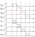
请参阅图6,栅极驱动器181a提供栅极扫描脉冲Vg_1~Vg_n,所述信号经过选择电路184与脉冲重整电路185对其进行处理以形成如图6中所示的触控扫描脉冲与压力扫描脉冲时序图(本发明所有时序图中仅以特定的几组时序图来表示电信号的变化趋势,其实际的时序图数量匹配于第一方向触控电极171、第二方向触控电极172以及压感单元161),Vg_1、Vg_2代表二不同像素单元91的栅极扫描脉冲之更新时序;Vt_1、Vt_2代表二不同触控单元175的触控扫描脉冲更新时序,信号处理电路15根据触控扫描脉冲之时序来侦测手指或触控笔等在上基板11上的触控点位置;Vf_1、Vf_2代表二不同的压感单元161的压力扫描脉冲更新时序,信号处理电路15根据压力扫描脉冲之时序来侦测触控点处所受到的按压力值。Please refer to FIG. 6, the
所述栅极扫描脉冲Vg_1和Vg_2、栅极扫描脉冲Vt_1和Vt_2以及压力扫描脉冲Vf_1与Vf_2之间相互错开,相互无时间间隙地彼此交替,即该三者分时序进行而可以避免相互之间的电性干扰。优选地在相邻栅极扫描脉冲与触控扫描脉冲之间,触控扫描脉冲以及压力扫描脉冲之间,栅极扫描脉冲以及压力扫描脉冲之间设置有时间间隙以避开彼此之间的电位切换点,因为在电位切换点处理讯号之间容易相互干扰,故,避开讯号之间的电位切换点可提升具有压力侦测的触控显示模组的抗噪性能。The gate scanning pulses Vg_1 and Vg_2, the gate scanning pulses Vt_1 and Vt_2, and the pressure scanning pulses Vf_1 and Vf_2 are staggered from each other, and alternate with each other without time gaps, that is, the three are performed in time sequence to avoid mutual interference. electrical interference. Preferably, a time gap is set between adjacent gate scan pulses and touch scan pulses, between touch scan pulses and pressure scan pulses, and between gate scan pulses and pressure scan pulses to avoid potentials between them Switching point, because signals processed at the potential switching point are likely to interfere with each other, so avoiding the potential switching point between signals can improve the anti-noise performance of the touch display module with pressure detection.
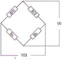
请参阅图7,压力信号处理器19包括一电桥191与一多路复用器192,多路复用器192包括第一多路复用器MUX1,第二多路复用器MUX2,电桥191包括至少一电阻Ra,至少一电阻Rb与一运算放大电路,第一多路复用器MUX1与第二多路复用器MUX2的输出端作为运算放大电路的输入信号U0分别电性连接于运算放大电路的同相输入端以及反向输入端,运算放大电路的输出端连接有滤波电路193以及ADC电路194,这样运算放大电路所输出的电信号可以通过滤波电路193进行去噪处理后再传递至ADC电路194进行模数转换。第一多路复用器MUX1的输出端连接在电阻Ra的一端,电阻Ra的另一端电性连接于激励源的正极端VEX+;第二多路复用器MUX2的输出端连接在电阻Rb的一端,电阻Rb的另一端电性连接于激励源的正极端VEX+;请注意,于本发明中电阻Ra和Rb属于电桥中固定共享的电阻,又称共享电阻。于相关实施例中,激励源的建置采用单电源或双电源供电方式但并非限定,而激励讯号可以采用方波、正弦波或定电压讯号等合适的给定讯号,讯号型态亦并不加以限定;优选地,激励源较佳可以采用本文每一实施例所揭示具方波型态扫描脉冲式的压力扫描脉冲作为激励源提供的信号,对压力传感器16进行激励并侦测变化。7, the
第一多路复用器MUX1的输入端连接的是压力传感器16的第一组多个压感单元161,所述第一组多个压感单元161对应的内阻为RF0,RF1,RF2······RFn,在用户触摸上基板11产生一定的压力时,位于上基板11之下的压感单元161所对应的内阻RF0,RF1,RF2······RFn阻值发生变化从而引起压力传感器16的压力信号的变化,第一多路复用器MUX1可以选择RF0,RF1,RF2······RFn的其中一个电阻作为其输入。The input end of the first multiplexer MUX1 is connected to the first group of multiple pressure-
第二多路复用器MUX2的输入端连接的是压力传感器16的第二组多个压感单元161,所述第二组多个压感单元161内阻为RC0,RC1,RC2······RCn,其与RF0,RF1,RF2······RFn一一匹配相邻设置,举例来说RC0设置在RF0的附近,RC1设置在RF1的附近,如此类推。RC0,RC1,RC2······RCn与RF0,RF1,RF2······RFn互为参考电阻而设置,第二多路复用器MUX2可以选择RC0,RC1,RC2······RCn的其中一个电阻作为其输入。在RF0,RF1,RF2······RFn所对应的压感单元161受到按压力时,RC0,RC1,RC2······RCn作为RF0,RF1,RF2······RFn的参考电阻;反之RC0,RC1,RC2······RCn所对应的压感单元161受到按压力时,RF0,RF1,RF2······RFn为RC0,RC1,RC2······RCn的参考电阻且它们一端连激励源的正极端VEX-。The input end of the second multiplexer MUX2 is connected to the second group of multiple
请参阅图8A,以第一多路复用器MUX1选择RF0与第二多路复用器MUX2选择RC0为例来对压力传感器16的工作原理进行说明。所述电阻RF0、电阻RC0以及电阻Ra与Rb构成了惠斯通电桥,在无按压力作用时,惠斯通电桥处于平衡状态。激励源为电桥191提供稳压电源,所述稳压电源在接入时不考虑其正负极极性,本实施例中优选直流稳压电源。当用户在上基板11操作时,其对上基板11有一个按压力,所述压力传感器16中对应内阻RF0,RF1,RF2······RFn一个或多个阻值改变,这样,惠斯通电桥平衡被打破而导致输出电信号U0必定发生变化,不同阻值的改变对应着不同的压力值,故,通过对惠斯通电桥的输出信号U0进行计算及处理即可以得出相应的压力值。实际上,我们也可以根据需要设置一个共享电阻来代替RC0,RC1,RC2······RCn。Referring to FIG. 8A , the working principle of the
于一选择性实施例中,如图8B所示,Ra及RC0也可以互换成为另一种形式的电桥。In an optional embodiment, as shown in FIG. 8B , Ra and RCO can also be exchanged into another form of electric bridge.
值得留意,于较佳实施例中,电阻(即如电阻Ra与Rb)可选用可变电阻,经由电路可程序动态调整,已达成动态调整与使相对应之多组RFn、RCn,Ra与Rb所构成的电桥平衡。It is worth noting that in a preferred embodiment, the resistors (such as resistors Ra and Rb) can be variable resistors, which can be dynamically adjusted through the circuit program, and the dynamic adjustment and corresponding multiple sets of RFn, RCn, Ra and Rb have been achieved. The formed bridge is balanced.
与现有技术相比,本发明所提供的具有压力侦测的触控显示模组10具有如下优点:Compared with the prior art, the
1.由于电容式触控面板采用的是人体感应电流的原理进行触控点侦测的,而当触控电极与压力侦测电极161设置在同一基材层14上且显示面板9靠近触控面板8时,元器件和导电线等之间的排布非常密切,讯号之间的相互干扰非常严重而导致触控点位置侦测及按压力值侦测不精准。本发明中巧妙的通过选择电路184和/或脉冲重整电路185将为像素单元91提供栅极驱动扫描脉冲的栅极驱动器181a加以利用,通过选择电路184和/或脉冲重整电路185进行选择,位移,脉宽缩窄以及分频等处理后提供压力扫描脉冲与触控扫描脉冲。栅极扫描脉冲,压力扫描脉冲与触控扫描脉冲之间可以分时序或同时序进行。同时序时,栅极扫描脉冲,压力扫描脉冲与触控扫描脉冲中的两者或三者同时进行,但它们之间的电位切换点相互错位(在电位切换点处,讯号极易受到外部干扰而导致电信号不稳定,讯号错位等等),这样使得具有压力侦测的触控显示模组10反应速度快,讯号之间的干扰降低,触控稳定性较好。在分时序时,栅极扫描脉冲,压力扫描脉冲与触控扫描脉冲分时段进行,故,电讯号之间的干扰也同样降低,具有压力侦测的触控显示模组10的触控稳定性得到大幅的提升。1. Since the capacitive touch panel uses the principle of human body induction current to detect touch points, when the touch electrodes and the
2.至少一屏蔽层位于所述多个像素单元91与多个触控单元171之间,和/或所述至少一压感单元161之间与触控单元171之间,所述屏蔽层可以有效地降低触控面板8与显示面板9之间、触控单元与压力单元之间的相互讯号干扰。2. At least one shielding layer is located between the plurality of
3.该具有压力侦测的触控显示模组10在进行显示的同时,其不仅能够侦测触控点位置,而且能够侦测到触控点的压力值。触控传感器17与压力传感器16的通过同一栅极驱动器181a来驱动,其节约了硬件成本,简化了电路设计,提升了具有压力侦测的触控显示模组10的集成度,且从一定程度上降低了具有压力侦测的触控显示模组10的厚度与重量。触控传感器17与压力传感器16以及显示面板9的导电线结构上靠近,现有技术中采用不同的驱动器分别对像素单元91,触控单元175与压感单元161进行驱动,其设计空间相比较小,元器件的排布密切不利于散热,本发明则很好地解决了这个问题。3. The
4.本发明中采用惠斯通电桥对按压力值进行侦测,其电路结构简单,控制精度高。最重要的所述压力信号处理器19中采用电桥191与多路复用器192结合,通过多路复用器192选择不同的压感单元161,但不同压感单元161在侦测压力信号时所构成的惠斯通电桥中,电阻Ra与Rb为共享电阻,这样设计可以大大地降低惠斯通电桥中的电阻数量,且不同压感单元161在进行压力侦测时,由于其部分硬件共享,故相互之间的误差率降低。更进一步,所述压感单元161所对应的内阻RF0,RF1,RF2······RFn一一对应设置有RC0,RC1,RC2······RCn互为参考电阻,该参考电阻设置在RF0,RF1,RF2······RFn附近,这样,它们之间的受到温度影响一致,受到的其他噪声也近似,这样有利于惠斯通电桥的稳定,降低了硬件电路因自身温度漂移,环境因素所带来的信号误判。RF0,RF1,RF2······RFn与RC0,RC1,RC2······RCn互为参考电阻,这样降低噪声的同时优化了资源的配置。惠斯通电桥的输出信号端接有运算放大电路,所述运算放大电路不仅可以将输出信号U0进行放大,且其可以利用运算放大电路抑制噪声的特性来降低噪声。以RF0与RC0为例来进行说明,在上基板11受到按压力时,RF0电阻值变化为△r,但实际上RF0受到如温度以及其他干扰而会产生△s的噪声,对于参考电阻RC0来说,其受到如温度以及其他干扰与其附近的RF0一致,大小也为△s的噪声,该噪声△s在运算放大电路的反向输入端经过反向后即与同向输入端的压敏电阻RF0的噪声相抵消,这样,大大的降低的其他噪声所带来的干扰,进一步提升了压力信号的侦测精度。实际上,于运算放大电路可能的噪声相抵消手法均可使用,例如,U=A((V+)-(V-))=A((V△r+V△s)-(-V△r+V△s))=2A V△r,△s系不受反向电压影响而存在的外部引发噪声效应,其中使用差动放大器或放大器组合皆为本发明可以采用的手法,并不以此为限,只要能消弭外部引发噪声效应的电路守法皆为本发明保护范围。4. In the present invention, a Wheatstone bridge is used to detect the pressure value, and the circuit structure is simple and the control precision is high. The most important thing is that the
5.本实施例中,在触控电极的非触控区174设置压感单元161,其通过绝缘块173的设置可以将压感单元161以及触控电极集成在同一平面,这样大大的降低了具有压力侦测的触控显示模组10的厚度,尤其是触控电极与压感单元161之间互补设置,可以使具有压力侦测的触控显示模组10的显示效果更佳。5. In this embodiment, the pressure-
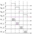
请参阅图9,本发明第二实施例提供一种具有压力侦测的触控显示模组(均未标号),所述具有压力侦测的触控显示模组与第一实施例的具有压力侦测的触控显示模组10的不同之处仅在于:所述的触控扫描脉冲与压力扫描脉冲以及栅极扫描脉冲的时序变化不一致,在本实施例中触控扫描脉冲与压力扫描脉冲均与栅极扫描脉冲同时序进行,但触控扫描脉冲与压力扫描脉冲之间分时序进行。压力扫描脉冲以及触控扫描脉冲的经驱动脉冲处理电路后脉宽变窄,这样,栅极扫描脉冲与压力扫描脉冲以及触控扫描脉冲之间存在时间间隙,举例来说,Vg_1中栅极扫描脉冲在t1和t2时刻切换电位,Vt_1中触控扫描脉冲脉宽小于栅极扫描脉冲脉宽,其在t3和t4时刻切换电位点,Vf_1中压力扫描脉冲脉宽小于栅极扫描脉冲脉宽,其在t5和t6时刻切换电位点,t1<t3<t4<t<t5<t6,像素单元、触控单元以及压感单元之间的运作的电位切换点彼此错开。在电位切换点,触控电极、压力传感器以及像素单元之间容易相互讯号干扰而导致触控点位置以及按压力值侦测不精准,本实施例则通过在栅极扫描脉冲、压力扫描脉冲与触控扫描脉冲设置一定的时间间隙使该两者的电位切换点错位来避免相互之间的讯号干扰。实际操作中所述触控扫描脉冲以及所述压力扫描脉冲之脉宽不宽于所述栅极驱动脉冲之脉宽即可。Please refer to FIG. 9 , the second embodiment of the present invention provides a touch display module with pressure detection (not labeled), the touch display module with pressure detection is the same as the touch display module with pressure detection in the first embodiment The detected
在本发明所有实施例中,所谓同时序即指在栅极扫描脉冲的一个工作周期(电位为“1”)内,压力扫描脉冲/触控扫描脉冲之工作周期与其存在重叠(不包括时序图的端点重叠)。反之,则为分时序。In all embodiments of the present invention, the so-called simultaneity means that within one working period of the gate scanning pulse (the potential is "1"), the working period of the pressure scanning pulse/touch scanning pulse overlaps with it (not including the timing diagram endpoints overlap). On the contrary, it is timing.
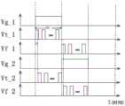
请参阅图10,本发明第三实施例提供一种具有压力侦测的触控显示模组(均未标号),所述具有压力侦测的触控显示模组与第二实施例的具有压力侦测的触控显示模组10的不同之处仅在于:所述的触控扫描脉冲与压力扫描脉冲的时序发生了变化,在本实施例中,触控扫描脉冲与压力扫描脉冲分时序进行,1个压力扫描脉冲及触控扫描脉冲包括多个短脉冲以降低噪声,图10中仅以3个短脉冲为例来进行说明,所述短脉冲也可以是2个或多个。Please refer to FIG. 10 , the third embodiment of the present invention provides a touch display module with pressure detection (not labeled), and the touch display module with pressure detection is the same as the touch display module with pressure detection in the second embodiment. The detected
请参阅图11a,本发明第四实施例提供一种具有压力侦测的触控显示模组(均未标号),所述具有压力侦测的触控显示模组与第一、二实施例的具有压力侦测的触控显示模组10的不同之处仅在于:在本实施例中,栅极扫描脉冲、触控扫描脉冲与压力扫描脉冲均同时序进行,在图10中,栅极扫描脉冲、触控扫描脉冲与压力扫描脉冲脉宽依次变窄以错开彼此电位切换点。举例来说,Vg_1中栅极扫描脉冲在t11和t21时刻切换电位,Vt_1中触控扫描脉冲脉宽小于Vg_1中栅极扫描脉冲脉宽,其在t31和t41时刻切换电位点,t11<t31,t21>t41,Vf_1中压力扫描脉冲脉宽小于Vt_1中触控扫描脉冲脉宽,且t51>t31,t61<t41,这样电位切换点进行了错位,即使产在生了干扰信号,它们之间也降低相互干扰的可能,如,压力扫描脉冲在电位切换点处产生了干扰讯号,但此时的栅极扫描脉冲与触控扫描脉冲正值稳定期,故,该干扰讯号对它们影响不大。栅极扫描脉冲、触控扫描脉冲与压力扫描脉冲在一工作周期内完全重叠,实际上,触控扫描脉冲与压力扫描脉冲脉宽不作限定,它们可以选择部分重叠而避开彼此的电位切换点,如图11b中所示,触控扫描脉冲与压力扫描脉冲均匀栅极扫描脉冲同时序进行,触控扫描脉冲与压力扫描脉冲相互之间也同时序但两者仅部分工作周期重叠。Please refer to FIG. 11a, the fourth embodiment of the present invention provides a touch display module with pressure detection (not labeled), the touch display module with pressure detection is the same as that of the first and second embodiments The
请参阅图12,本发明第五实施例提供一种具有压力侦测的触控显示模组(均未标号),所述具有压力侦测的触控显示模组与第一至四实施例的具有压力侦测的触控显示模组的不同之处仅在于:触控扫描脉冲的脉宽变窄,其错开了栅极扫描脉冲的电位切换点,压力扫描脉冲的脉宽比触控扫描脉冲频率更窄且电位切换点也错开了,设定栅极扫描脉冲频率为Fg,触控扫描脉冲频率为Ft,压力扫描脉冲频率为Ff,Fg>Ft>Ff。由于具有压力侦测的触控显示模组依次对像素单元,触控单元以及压感单元的扫描脉宽要求要依次降低,故,相对于栅极扫描脉冲的扫描频率来依次降低触控扫描脉冲以及压力扫描脉冲的扫描脉宽同样可以达到触控点与按压力侦测的目的,且这样降低了具有压力侦测的触控显示模组的能耗。优选地,Fg=(1-20)Ft,Fg=(1-50)Ff。Please refer to FIG. 12 , the fifth embodiment of the present invention provides a touch display module with pressure detection (not labeled), the touch display module with pressure detection is the same as that of the first to fourth embodiments The touch display module with pressure detection is only different in that: the pulse width of the touch scan pulse is narrowed, which staggers the potential switching point of the gate scan pulse, and the pulse width of the pressure scan pulse is wider than that of the touch scan pulse. The frequency is narrower and the potential switching point is also staggered. Set the grid scan pulse frequency as Fg, the touch scan pulse frequency as Ft, and the pressure scan pulse frequency as Ff, where Fg>Ft>Ff. Since the touch display module with pressure detection sequentially reduces the scanning pulse width requirements of the pixel unit, the touch unit and the pressure-sensing unit, the touch scanning pulse is sequentially reduced relative to the scanning frequency of the gate scanning pulse And the scanning pulse width of the pressure scanning pulse can also achieve the purpose of touch point and pressing force detection, and thus reduce the energy consumption of the touch display module with pressure detection. Preferably, Fg=(1-20)Ft, Fg=(1-50)Ff.
请参阅图13,本发明第六实施例提供一种具有压力侦测的触控显示模组(未标号),所述具有压力侦测的触控显示模组与第一至五实施例的具有压力侦测的触控显示模组10的不同之处仅在于:该具有压力侦测的触控显示模组之驱动脉冲处理电路687包括多路选择电路与脉冲重整电路:第一选择电路684a,第一脉冲重整电路685b,第二选择电路684a,第二脉冲重整电路685b······第n选择电路684a以及第n脉冲重整电路685n,不同组选择电路及脉冲重整电路为不同的触控电极与压感单元分别提供触控扫描脉冲与压力扫描脉冲。Please refer to FIG. 13 , the sixth embodiment of the present invention provides a touch display module with pressure detection (not labeled), the touch display module with pressure detection is the same as that of the first to fifth embodiments The pressure detection
请参阅图14,以2组触控单元及压感单元与像素单元(均未标号)为例来对驱动脉冲处理电路687所输出的栅极触控扫描脉冲和触控扫描脉冲与压力扫描脉冲来进行说明,设定:Vg_1与Vg_2分别是显示面板9像素单元1与像素单元2所接收到的栅极扫描脉冲,Vt_1与Vt_2分别是触控传感器66上的触控单元1与触控单元2所接收到的触控扫描脉冲信号,Vf_1与Vf_2分别是压力传感器67上的压感单元1和压感单元2所接收到的压力扫描脉冲信号与触控扫描脉冲以及压力扫描脉冲分时序进行。触控扫描脉冲的一个脉冲周期为tz,其由多个短脉冲td组成,触控单元1与触控单元2之间的触控极扫描脉冲起始电位切换点之间存在ts(ts<tz,ts≠ntd,n为正整数)的延迟,故,触控素单元1与触控单元2之间的触控扫描脉冲的电位切换点进行了错位。同样的,压感单元1与压感单元2之间的压力扫描脉冲也进行了电位切换点的错位。触控单元以及压感单元之间的电讯号干扰降低,且由于多组选择电路与脉冲重整电路对栅极扫描脉冲进行处理来为压感单元以及触控单元同时提供压力扫描脉冲及触控扫描脉冲,故,其工作周期缩短,电讯号之间的相互干扰也降低。本实施例中的电位切换点错位技术同样适用于其他实施例。Please refer to FIG. 14 , taking two groups of touch units, pressure sensing units and pixel units (not labeled) as an example to control the gate touch scan pulse, touch scan pulse and pressure scan pulse output by the driving
请参阅图15,本发明第七实施例提供一种具有压力侦测的触控显示模组(未标号),所述具有压力侦测的触控显示模组与第一至六实施例的具有压力侦测的触控显示模组10的不同之处仅在于:所述触控电极(未标号)之间无交叠区域,即第一方向触控电极771与第二方向触控电极772之间无交叠区域,且在该两者之间的所形成的非触控区774内设置有压感单元761,这样可以避免触控电极之间、触控电极与压感单元761之间因交叠所带来的线路易断裂的问题。最佳地,所述第一方向触控电极771、第二方向触控电极772以及压感单元761之间互补设计。第一方向触控电极771与第二方向触控电极772的图案形状不作限定,其可以是矩形,三角形或其他不规则的形状。Please refer to FIG. 15 , the seventh embodiment of the present invention provides a touch display module with pressure detection (not labeled), the touch display module with pressure detection is the same as that of the first to sixth embodiments The
请参阅图16A,本发明第八实施例提供一种具有压力侦测的触控显示模组80,所述具有压力侦测的触控显示模组80与第一至七实施例的具有压力侦测的触控显示模组10的不同之处仅在于:该具有压力侦测的触控显示模组80从上至下包括一上基板81,一贴合层82,一第一电极图案层83,一第一基材层84,一第二电极图案层86,一第二基材层87,一信号处理电路85与一显示面板7,第一基材层84与第二基材层87分别作为第一电极图案层83与第二电极图案层86的承载层,第一基材层84通过贴合层82与上基板81贴合。其中,第一基材层84与第二基材层87分别可以为不同应力系数的柔性基材,也因此各自设置于差异化应力系数的柔性基材的压感单元于按压时能有不同的信号感应量以提升压感灵敏度。第一电极图案层83与第二电极图案层86以及显示面板7通过导电线(图未视)电连接于信号处理电路85。该信号处理电路85位置不作限定,其可以设置在第二基材层87的下方或者其上方或者一侧。Please refer to FIG. 16A , the eighth embodiment of the present invention provides a
请参阅图16B,第一电极图案层83包括多条相互平行的第一方向触控电极871,在所述多条第一方向触控电极871之间设置有非触控区域874,所述非触控区域874内设置有压感单元861。所述第二电极图案层86上表面或下表面设置有多条相互平行的第二方向触控电极(未标号)。第一方向触控电极871与第二方向触控电极分层设置可避免触控电极之间因交叠所带来的线路易断裂的问题。Please refer to FIG. 16B , the first
第二电极图案层86也可以设置在第一基材层84的下表面,或第一电极图案层83直接设置在上基板81上,第二电极图案层86设置在第一基材层84上,这样既可以减少第二基材层87的设置,可以把具有压力侦测的触控显示模组80做的更薄。The second
请参阅图17,本发明第九实施例提供一种具有压力侦测的触控显示模组90,所述具有压力侦测的触控显示模组90与第一至八实施例的具有压力侦测的触控显示模组10的不同之处仅在于:本实施例中具有压力侦测的触控显示模组90增设了一第二压力层96,具有压力侦测的触控显示模组90从上至下包括一上基板91,一贴合层92,一电极图案层93,一第一基材层94,一第二压力层96,一第二基材层97,一信号处理电路95以及一显示面板6,界定所述电极图案层93上的多个压感单元(未标号)形成的是第一压力层(未标号),本实施例增设了第二压力层96,我们可以通过两层的压力层侦测结果的叠加以更加精准地侦测按压力值。Please refer to FIG. 17 , the ninth embodiment of the present invention provides a
请参阅图18A-18B,作为具有压力侦测的触控显示模组90的变形:图18A中,第一压力层96a与一第二压力层96a’以及触控传感器97a由上至下依次设置在第一基材层94a、第二基材层94a’和第三基材层94a”上。第一压力层96a与一第二压力层96a’,触控传感器97a以及显示面板6a之间可以设置至少一屏蔽层。请参阅图18B,其与图18A的不同之处仅在于所述第一压力层96b与一第二压力层96b’设置于同一基材层94b的上下表面上。于较佳实施例中,屏蔽层为一金属层外,另可选择性地配合像素单元设计进行镂空设计,以提高具有压力侦测的触控显示模组90的整体透光率。Please refer to FIGS. 18A-18B , as a deformation of the
请参阅图19,位于第一压力层与一第二压力层96上的压感单元961之间优选为偏移及错排而不完全对应。第一压力层上压感单元961在对应的第二压力层96之压感单元961上的垂直投影面积为单个压感单元961面积的10%-90%,优选地为50%-80%。Please refer to FIG. 19 , the
请参阅图20,以2组像素单元,触控单元及压感单元为例来对驱动脉冲处理电路(图未视)所输出的触控扫描脉冲与压力扫描脉冲来进行说明,设定Vt_1与Vt_2分别是触控电极1与触控电极2所接收到的触控扫描脉冲信号,Vg_1与Vg_2分别是像素单元1与像素单元2所接收到的栅极扫描脉冲,Vt_1与Vt_2分别是触控单元1与触控单元2所接收到的触控扫描脉冲信号,Vf_1与Vf_2分别是第一压力层上压感单元1和压感单元2所接收到的压力扫描脉冲信号,Vf_a与Vf_b分别是第二压力层96上的压感单元a与压感单b所接收到的压力扫描脉冲信号,触控扫描脉冲,第一压力层上压感单元所接收到的压力扫描脉冲以及第二压力层上压感单元所接收到的压力扫描脉冲分别分时序进行,但它们与栅极扫描脉冲为同时序进行。触控扫描脉冲,第一压力层上压感单元所接收到的压力扫描脉冲以及第二压力层上压感单元所接收到的压力扫描脉冲的脉宽缩窄以避开彼此的电位切换点以提升讯号之间的抗干扰性能,当然此处也可以不进行脉宽缩窄。压力扫描脉冲或触控扫描脉冲也可以包括多个短脉冲。Please refer to FIG. 20 , taking two groups of pixel units, a touch unit and a pressure sensing unit as an example to illustrate the touch scan pulse and pressure scan pulse output by the drive pulse processing circuit (not shown in the figure), set Vt_1 and Vt_2 is the touch scan pulse signal received by
请参阅图21,本发明第十实施例提供一种具有压力侦测的触控显示模组(均未标号),所述具有压力侦测的触控显示模组与八实施例的具有压力侦测的触控显示模组90的不同之处仅在于:触控扫描脉冲脉宽缩窄与栅极扫描脉冲同时序进行,第一压力层与第二压力层的压力扫描脉冲与栅极扫描脉冲同时序进行但与触控扫描脉冲分时序进行。第一压力层的压力扫描脉冲脉宽窄于与第二压力层的压力扫描脉冲之脉宽。栅极扫描脉冲,触控扫描脉冲,压力扫描脉冲之间的电位切换点均错开,这样讯号之间的干扰降低。实际上,触控电极与第一压力层以及第二压力层的扫描脉宽不作限定,只要保证触控电极与第一压力层以及第二压力层之间的扫描脉冲之电位切换点错开即可。触控扫描脉冲,第一压力层的压力扫描脉冲与第二压力层的压力扫描脉冲中的一项或多项可以同时序进行。Please refer to FIG. 21 , the tenth embodiment of the present invention provides a touch display module with pressure detection (not labeled), the touch display module with pressure detection is the same as the touch display module with pressure detection in the eighth embodiment The
请参阅图22,本发明第十一实施例提供一种具有压力侦测的触控显示模组(均未标号),所述具有压力侦测的触控显示模组与八实施例的具有压力侦测的触控显示模组90的不同之处仅在于:栅极扫描脉冲,触控扫描脉冲以及第一压力层与第二压力层的压力扫描脉冲脉宽依次缩窄后同时序进行,且它们之间的工作周期完全重叠但电位切换点错位。Please refer to FIG. 22 , the eleventh embodiment of the present invention provides a touch display module with pressure detection (not labeled), and the touch display module with pressure detection is the same as the touch display module with pressure detection in the eighth embodiment. The detected
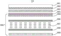
请参阅图23,本发明的第十二实施例的具有压力侦测的触控显示模组99从上至下包括一盖板991,一贴合层992,一压力层993,以及一触控显示面板990,所述触控显示面板990从上至下依次包括一上偏光片994,一触控电极层995,一上基板996,一液晶层997,一下基板998和一下偏光片999,上基板996和下基板998夹持液晶层997,触控电极层995位置不作限定,其可以设置在上偏光片994的下表面,或上基板996上表面/下表面,或下基板998上表面/下表面、或下偏光片999下表面上。该触控电极层995包括多条第一方向触控电极(图未视)和多条第二方向触控电极(图未视),所述多条第一方向触控电极和多条第二方向触控电极可以分别设置在上偏光片994的下表面,上基板996上表面/下表面,下基板998上表面/下表面、下偏光片999下表面中的任意两个表面上。压力层993与盖板991之间通过贴合层992贴合后直接与显示面板990贴合即可。这样,可以快速地在嵌入式(例如On-cell或In-cell)结构的触控显示面板上加载压力层993,使具有压力侦测的触控显示模组99具有触控显示功能的同时具有侦测触控点按压力值的功能。Please refer to FIG. 23, the
本发明第十三实施例提供一种具有压力侦测的触控显示模组之驱动方法,该具有压力侦测的触控显示模组包括阵列设置的多个像素单元及一三维传感器,所述三维传感器包括多个触控单元与至少一压感单元,所述触控显示模组可以是本发明中实施例一至实施例十二中所提及的任一种触控显示模组(本实施例中所提及的机械元器件名称及其标号参考实施例一中的机械元器件命名及其标号),该触控显示模组之驱动方法包括步骤:The thirteenth embodiment of the present invention provides a method for driving a touch display module with pressure detection. The touch display module with pressure detection includes a plurality of pixel units arranged in an array and a three-dimensional sensor. The three-dimensional sensor includes a plurality of touch units and at least one pressure-sensitive unit, and the touch display module can be any touch display module mentioned in
S1:提供一栅极驱动扫描脉冲至像素单元91以控制其显示色彩更新时序;S1: providing a gate driving scan pulse to the
S2:提供一触控扫描脉冲至触控单元175以控制侦测触控点的时序;及S2: providing a touch scan pulse to the
S3:提供一压力扫描脉冲至压感单元161以控制侦测按压力的时序;S3: providing a pressure scanning pulse to the
其中,所述栅极驱动脉冲,触控扫描脉冲以及压力扫描脉冲之间的电位切换点错开。Wherein, the potential switching points among the gate driving pulse, the touch scanning pulse and the pressure scanning pulse are staggered.
其中,触控扫描脉冲以及压力扫描脉冲可以分时序进行,也可以同时序进行。Wherein, the touch scanning pulse and the pressure scanning pulse can be performed in a time sequence, or can be performed in a simultaneous sequence.
与现有设计相比,本发明所提供的触控显示模组之驱动方法通过电位切换点的错位可以达到优越的抗噪性能。Compared with the existing design, the driving method of the touch display module provided by the present invention can achieve superior anti-noise performance through the dislocation of the potential switching point.
以上所述仅为本发明的较佳实施例而已,并不用以限制本发明,凡在本发明的原则之内所作的任何修改,等同替换和改进等均应包含本发明的保护范围之内。The above descriptions are only preferred embodiments of the present invention, and are not intended to limit the present invention. Any modifications, equivalent replacements and improvements within the principles of the present invention shall be included within the protection scope of the present invention.
Claims (20)
Priority Applications (4)
| Application Number | Priority Date | Filing Date | Title |
|---|---|---|---|
| CN201510404705.4ACN106325631B (en) | 2015-07-10 | 2015-07-10 | A touch display module with pressure detection and its driving method |
| TW105208700UTWM529885U (en) | 2015-07-10 | 2016-06-08 | Touch display module having pressure detection mechanism |
| TW105118172ATWI627567B (en) | 2015-07-10 | 2016-06-08 | Touch display module having pressure detection mechanism and driving method of the same |
| US15/206,307US10261614B2 (en) | 2015-07-10 | 2016-07-10 | Touch display module having pressure detection mechanism |
Applications Claiming Priority (1)
| Application Number | Priority Date | Filing Date | Title |
|---|---|---|---|
| CN201510404705.4ACN106325631B (en) | 2015-07-10 | 2015-07-10 | A touch display module with pressure detection and its driving method |
Publications (2)
| Publication Number | Publication Date |
|---|---|
| CN106325631A CN106325631A (en) | 2017-01-11 |
| CN106325631Btrue CN106325631B (en) | 2023-03-07 |
Family
ID=57726215
Family Applications (1)
| Application Number | Title | Priority Date | Filing Date |
|---|---|---|---|
| CN201510404705.4AExpired - Fee RelatedCN106325631B (en) | 2015-07-10 | 2015-07-10 | A touch display module with pressure detection and its driving method |
Country Status (3)
| Country | Link |
|---|---|
| US (1) | US10261614B2 (en) |
| CN (1) | CN106325631B (en) |
| TW (2) | TWM529885U (en) |
Families Citing this family (34)
| Publication number | Priority date | Publication date | Assignee | Title |
|---|---|---|---|---|
| KR101793857B1 (en) | 2010-04-13 | 2017-11-03 | 지이 비디오 컴프레션, 엘엘씨 | Inheritance in sample array multitree subdivision |
| CN106067983B (en) | 2010-04-13 | 2019-07-12 | Ge视频压缩有限责任公司 | The method of decoding data stream, the method and decoder for generating data flow |
| CN106231323B (en) | 2010-04-13 | 2020-07-28 | Ge视频压缩有限责任公司 | Decoder, decoding method, encoder, and encoding method |
| KR102669292B1 (en)* | 2010-04-13 | 2024-05-28 | 지이 비디오 컴프레션, 엘엘씨 | Sample region merging |
| CN106325631B (en)* | 2015-07-10 | 2023-03-07 | 宸鸿科技(厦门)有限公司 | A touch display module with pressure detection and its driving method |
| CN105677112B (en)* | 2016-02-24 | 2019-01-18 | 上海天马微电子有限公司 | Touch display panel and touch display device |
| KR102555596B1 (en)* | 2016-06-21 | 2023-07-17 | 삼성디스플레이 주식회사 | Electronic apparatus |
| KR102565939B1 (en)* | 2016-07-05 | 2023-08-11 | 삼성디스플레이 주식회사 | Touch sensor and display device having the same |
| KR102667249B1 (en) | 2016-10-31 | 2024-05-17 | 엘지디스플레이 주식회사 | Display apparatus for sensing a press |
| CN106328685B (en)* | 2016-10-31 | 2019-08-02 | 上海天马有机发光显示技术有限公司 | Organic light emitting display panel and display device comprising it |
| CN108572755A (en) | 2017-03-13 | 2018-09-25 | 义隆电子股份有限公司 | Pointing input device, signal processing device thereof and pointing input module |
| TWI643102B (en)* | 2017-03-13 | 2018-12-01 | 義隆電子股份有限公司 | Pointing input device and its signal processing device, pointing input module |
| CN107315502B (en)* | 2017-06-30 | 2020-05-19 | 上海天马微电子有限公司 | Display panel, display device and pressure detection method |
| CN107479743B (en)* | 2017-07-28 | 2020-08-18 | 上海天马微电子有限公司 | Display substrate, display panel and display device |
| CN107393497A (en)* | 2017-08-30 | 2017-11-24 | 上海天马微电子有限公司 | Display panel and display device |
| CN107656643B (en)* | 2017-09-26 | 2020-08-11 | 厦门天马微电子有限公司 | Display panel and electronic equipment |
| JP2019067141A (en)* | 2017-09-29 | 2019-04-25 | 株式会社ジャパンディスプレイ | Detection device and display device |
| CN107562285B (en)* | 2017-10-25 | 2020-08-14 | 厦门天马微电子有限公司 | Display panel, pressure detection method thereof and display device |
| CN107643854B (en)* | 2017-10-31 | 2020-10-09 | 上海天马微电子有限公司 | Array substrate, display panel and display device |
| TWI728275B (en)* | 2017-11-03 | 2021-05-21 | 瑞鼎科技股份有限公司 | Organic light-emitting diode touch display operating method |
| CN108198530A (en)* | 2018-01-03 | 2018-06-22 | 厦门天马微电子有限公司 | A kind of display panel and its driving method, display device |
| CN108597424B (en)* | 2018-01-08 | 2021-03-23 | 厦门天马微电子有限公司 | Display panel, display device and detection method |
| CN108446050B (en)* | 2018-03-16 | 2021-06-15 | 厦门天马微电子有限公司 | Pressure sensor, display panel, pressure detection method and display device |
| CN108693993B (en)* | 2018-03-28 | 2021-04-02 | 厦门天马微电子有限公司 | Touch substrate, touch display panel and touch display device |
| CN108510953B (en)* | 2018-04-17 | 2021-11-26 | 厦门天马微电子有限公司 | Display panel and display device |
| KR102647742B1 (en)* | 2018-10-15 | 2024-03-14 | 삼성디스플레이 주식회사 | Touch sensor and display device |
| CN109558799B (en)* | 2018-10-26 | 2022-04-15 | 国微集团(深圳)有限公司 | Fingerprint acquisition method and device and product adopting fingerprint acquisition device |
| KR102783612B1 (en)* | 2019-01-30 | 2025-03-19 | 삼성디스플레이 주식회사 | Touch sensor and display device |
| CN112445273B (en)* | 2019-08-29 | 2024-06-25 | 华硕电脑股份有限公司 | Electronic device and pressure sensing touch control assembly thereof |
| JP7567814B2 (en)* | 2020-01-31 | 2024-10-16 | ソニーグループ株式会社 | Sensor Modules and Electronic Devices |
| TWI724906B (en)* | 2020-05-20 | 2021-04-11 | 晶田科技有限公司 | Intelligent TFT touch sensing device and information processing device using it |
| TW202437081A (en) | 2021-01-29 | 2024-09-16 | 南韓商希迪普公司 | Touch device, driving method the same and touch system |
| CN114168012B (en)* | 2021-12-08 | 2023-12-15 | 京东方科技集团股份有限公司 | Driving circuit, driving method thereof and touch display device |
| TWI827364B (en)* | 2022-11-15 | 2023-12-21 | 達運精密工業股份有限公司 | Electronic switch device and system thereof |
Citations (2)
| Publication number | Priority date | Publication date | Assignee | Title |
|---|---|---|---|---|
| CN101291111A (en)* | 2007-04-06 | 2008-10-22 | 电力集成公司 | Method and apparatus for sensing multiple voltage values from a single terminal of a power converter controller |
| CN102340245A (en)* | 2010-04-29 | 2012-02-01 | 电力集成公司 | Apparatus and method for sensing of isolated power converter output |
Family Cites Families (9)
| Publication number | Priority date | Publication date | Assignee | Title |
|---|---|---|---|---|
| CN201107503Y (en)* | 2007-11-21 | 2008-08-27 | 宸鸿光电科技股份有限公司 | Touch display panel with electric field shielding layer |
| TWI395008B (en)* | 2009-10-22 | 2013-05-01 | Au Optronics Corp | Touch panel and touch display device |
| TW201205369A (en)* | 2010-07-20 | 2012-02-01 | Novatek Microelectronics Corp | Driving method, driving device and touch sensible display device using the same |
| US8698769B2 (en)* | 2011-08-01 | 2014-04-15 | Sharp Kabushiki Kaisha | Dual mode capacitive touch panel |
| US9246486B2 (en)* | 2011-12-16 | 2016-01-26 | Apple Inc. | Electronic device with noise-cancelling force sensor |
| KR101472806B1 (en)* | 2012-01-30 | 2014-12-15 | 삼성디스플레이 주식회사 | Touch panel and display device having a touch panel |
| WO2014018116A1 (en)* | 2012-07-26 | 2014-01-30 | Changello Enterprise Llc | Ultrasound-based force sensing and touch sensing |
| US9195354B2 (en)* | 2013-03-12 | 2015-11-24 | Synaptics Incorporated | Device and method for localized force and proximity sensing |
| CN106325631B (en)* | 2015-07-10 | 2023-03-07 | 宸鸿科技(厦门)有限公司 | A touch display module with pressure detection and its driving method |
- 2015
- 2015-07-10CNCN201510404705.4Apatent/CN106325631B/ennot_activeExpired - Fee Related
- 2016
- 2016-06-08TWTW105208700Upatent/TWM529885U/ennot_activeIP Right Cessation
- 2016-06-08TWTW105118172Apatent/TWI627567B/enactive
- 2016-07-10USUS15/206,307patent/US10261614B2/enactiveActive
Patent Citations (2)
| Publication number | Priority date | Publication date | Assignee | Title |
|---|---|---|---|---|
| CN101291111A (en)* | 2007-04-06 | 2008-10-22 | 电力集成公司 | Method and apparatus for sensing multiple voltage values from a single terminal of a power converter controller |
| CN102340245A (en)* | 2010-04-29 | 2012-02-01 | 电力集成公司 | Apparatus and method for sensing of isolated power converter output |
Also Published As
| Publication number | Publication date |
|---|---|
| TWI627567B (en) | 2018-06-21 |
| TWM529885U (en) | 2016-10-01 |
| US20170010730A1 (en) | 2017-01-12 |
| CN106325631A (en) | 2017-01-11 |
| US10261614B2 (en) | 2019-04-16 |
| TW201702843A (en) | 2017-01-16 |
Similar Documents
| Publication | Publication Date | Title |
|---|---|---|
| CN106325631B (en) | A touch display module with pressure detection and its driving method | |
| US11327615B2 (en) | Touch panel and apparatus for driving thereof | |
| US10365751B2 (en) | Display device with three-dimension input module | |
| CN204904241U (en) | Display device containing three -dimensional input module | |
| CN105117089B (en) | Touch base plate, touch-control display panel and its driving method, touch control display apparatus | |
| CN106557207B (en) | Touch display panel and sensing driving method thereof | |
| CN105786251B (en) | Display panel, driving method thereof, and display device | |
| TWI603243B (en) | Touch assembly with pressure detection and driving method thereof | |
| CN205375417U (en) | Touch -control display module assembly with pressure is listened | |
| WO2017118017A1 (en) | Touch-control panel, touch-control display apparatus and driving method thereof | |
| KR101360782B1 (en) | Display device with integrated touch screen | |
| WO2014131248A1 (en) | Capacitive in-cell touch panel and display device | |
| CN105549790A (en) | A pressure sensing touch module | |
| CN205353969U (en) | Touch -control assembly with pressure is listened | |
| CN107193427B (en) | Display device | |
| WO2017020344A1 (en) | Mutual-capacitance touch unit, touch liquid crystal panel, and driving method | |
| CN109669568B (en) | Active matrix touch panel with narrow bezel | |
| CN108196723B (en) | display panel | |
| CN107422896B (en) | Touch display panel, driving method thereof and display device | |
| CN104407761A (en) | Touch display panel, driving method of touch display panel and touch display device | |
| CN205193765U (en) | Array substrate , touch -control display panel | |
| CN106339117B (en) | Display device comprising three-dimensional input module | |
| US10318037B2 (en) | Detection method for enhanced 3D detection module | |
| TWI614663B (en) | Touch detection method of capacitive 3d detection module | |
| TWI503722B (en) | Touch display apparatus |
Legal Events
| Date | Code | Title | Description |
|---|---|---|---|
| PB01 | Publication | ||
| PB01 | Publication | ||
| C10 | Entry into substantive examination | ||
| SE01 | Entry into force of request for substantive examination | ||
| GR01 | Patent grant | ||
| GR01 | Patent grant | ||
| CF01 | Termination of patent right due to non-payment of annual fee | Granted publication date:20230307 | |
| CF01 | Termination of patent right due to non-payment of annual fee |