CN106256017B - Semiconductor device and display device including the same - Google Patents
Semiconductor device and display device including the sameDownload PDFInfo
- Publication number
- CN106256017B CN106256017BCN201580020352.6ACN201580020352ACN106256017BCN 106256017 BCN106256017 BCN 106256017BCN 201580020352 ACN201580020352 ACN 201580020352ACN 106256017 BCN106256017 BCN 106256017B
- Authority
- CN
- China
- Prior art keywords
- film
- insulating film
- oxide semiconductor
- transistor
- oxygen
- Prior art date
- Legal status (The legal status is an assumption and is not a legal conclusion. Google has not performed a legal analysis and makes no representation as to the accuracy of the status listed.)
- Expired - Fee Related
Links
Images


Classifications
- G—PHYSICS
- G02—OPTICS
- G02F—OPTICAL DEVICES OR ARRANGEMENTS FOR THE CONTROL OF LIGHT BY MODIFICATION OF THE OPTICAL PROPERTIES OF THE MEDIA OF THE ELEMENTS INVOLVED THEREIN; NON-LINEAR OPTICS; FREQUENCY-CHANGING OF LIGHT; OPTICAL LOGIC ELEMENTS; OPTICAL ANALOGUE/DIGITAL CONVERTERS
- G02F1/00—Devices or arrangements for the control of the intensity, colour, phase, polarisation or direction of light arriving from an independent light source, e.g. switching, gating or modulating; Non-linear optics
- G02F1/01—Devices or arrangements for the control of the intensity, colour, phase, polarisation or direction of light arriving from an independent light source, e.g. switching, gating or modulating; Non-linear optics for the control of the intensity, phase, polarisation or colour
- G02F1/13—Devices or arrangements for the control of the intensity, colour, phase, polarisation or direction of light arriving from an independent light source, e.g. switching, gating or modulating; Non-linear optics for the control of the intensity, phase, polarisation or colour based on liquid crystals, e.g. single liquid crystal display cells
- G02F1/133—Constructional arrangements; Operation of liquid crystal cells; Circuit arrangements
- G02F1/136—Liquid crystal cells structurally associated with a semi-conducting layer or substrate, e.g. cells forming part of an integrated circuit
- G02F1/1362—Active matrix addressed cells
- G02F1/1368—Active matrix addressed cells in which the switching element is a three-electrode device
- H—ELECTRICITY
- H10—SEMICONDUCTOR DEVICES; ELECTRIC SOLID-STATE DEVICES NOT OTHERWISE PROVIDED FOR
- H10D—INORGANIC ELECTRIC SEMICONDUCTOR DEVICES
- H10D30/00—Field-effect transistors [FET]
- H10D30/60—Insulated-gate field-effect transistors [IGFET]
- H10D30/67—Thin-film transistors [TFT]
- H10D30/6704—Thin-film transistors [TFT] having supplementary regions or layers in the thin films or in the insulated bulk substrates for controlling properties of the device
- H10D30/6713—Thin-film transistors [TFT] having supplementary regions or layers in the thin films or in the insulated bulk substrates for controlling properties of the device characterised by the properties of the source or drain regions, e.g. compositions or sectional shapes
- H—ELECTRICITY
- H10—SEMICONDUCTOR DEVICES; ELECTRIC SOLID-STATE DEVICES NOT OTHERWISE PROVIDED FOR
- H10D—INORGANIC ELECTRIC SEMICONDUCTOR DEVICES
- H10D30/00—Field-effect transistors [FET]
- H10D30/60—Insulated-gate field-effect transistors [IGFET]
- H10D30/67—Thin-film transistors [TFT]
- H10D30/6729—Thin-film transistors [TFT] characterised by the electrodes
- H10D30/673—Thin-film transistors [TFT] characterised by the electrodes characterised by the shapes, relative sizes or dispositions of the gate electrodes
- H10D30/6733—Multi-gate TFTs
- H10D30/6734—Multi-gate TFTs having gate electrodes arranged on both top and bottom sides of the channel, e.g. dual-gate TFTs
- H—ELECTRICITY
- H10—SEMICONDUCTOR DEVICES; ELECTRIC SOLID-STATE DEVICES NOT OTHERWISE PROVIDED FOR
- H10D—INORGANIC ELECTRIC SEMICONDUCTOR DEVICES
- H10D30/00—Field-effect transistors [FET]
- H10D30/60—Insulated-gate field-effect transistors [IGFET]
- H10D30/67—Thin-film transistors [TFT]
- H10D30/674—Thin-film transistors [TFT] characterised by the active materials
- H10D30/6755—Oxide semiconductors, e.g. zinc oxide, copper aluminium oxide or cadmium stannate
- H—ELECTRICITY
- H10—SEMICONDUCTOR DEVICES; ELECTRIC SOLID-STATE DEVICES NOT OTHERWISE PROVIDED FOR
- H10D—INORGANIC ELECTRIC SEMICONDUCTOR DEVICES
- H10D30/00—Field-effect transistors [FET]
- H10D30/60—Insulated-gate field-effect transistors [IGFET]
- H10D30/67—Thin-film transistors [TFT]
- H10D30/6757—Thin-film transistors [TFT] characterised by the structure of the channel, e.g. transverse or longitudinal shape or doping profile
- H—ELECTRICITY
- H10—SEMICONDUCTOR DEVICES; ELECTRIC SOLID-STATE DEVICES NOT OTHERWISE PROVIDED FOR
- H10D—INORGANIC ELECTRIC SEMICONDUCTOR DEVICES
- H10D86/00—Integrated devices formed in or on insulating or conducting substrates, e.g. formed in silicon-on-insulator [SOI] substrates or on stainless steel or glass substrates
- H10D86/40—Integrated devices formed in or on insulating or conducting substrates, e.g. formed in silicon-on-insulator [SOI] substrates or on stainless steel or glass substrates characterised by multiple TFTs
- H10D86/421—Integrated devices formed in or on insulating or conducting substrates, e.g. formed in silicon-on-insulator [SOI] substrates or on stainless steel or glass substrates characterised by multiple TFTs having a particular composition, shape or crystalline structure of the active layer
- H10D86/423—Integrated devices formed in or on insulating or conducting substrates, e.g. formed in silicon-on-insulator [SOI] substrates or on stainless steel or glass substrates characterised by multiple TFTs having a particular composition, shape or crystalline structure of the active layer comprising semiconductor materials not belonging to the Group IV, e.g. InGaZnO
- H—ELECTRICITY
- H10—SEMICONDUCTOR DEVICES; ELECTRIC SOLID-STATE DEVICES NOT OTHERWISE PROVIDED FOR
- H10D—INORGANIC ELECTRIC SEMICONDUCTOR DEVICES
- H10D86/00—Integrated devices formed in or on insulating or conducting substrates, e.g. formed in silicon-on-insulator [SOI] substrates or on stainless steel or glass substrates
- H10D86/40—Integrated devices formed in or on insulating or conducting substrates, e.g. formed in silicon-on-insulator [SOI] substrates or on stainless steel or glass substrates characterised by multiple TFTs
- H10D86/60—Integrated devices formed in or on insulating or conducting substrates, e.g. formed in silicon-on-insulator [SOI] substrates or on stainless steel or glass substrates characterised by multiple TFTs wherein the TFTs are in active matrices
- H—ELECTRICITY
- H10—SEMICONDUCTOR DEVICES; ELECTRIC SOLID-STATE DEVICES NOT OTHERWISE PROVIDED FOR
- H10D—INORGANIC ELECTRIC SEMICONDUCTOR DEVICES
- H10D99/00—Subject matter not provided for in other groups of this subclass
Landscapes
- Physics & Mathematics (AREA)
- Nonlinear Science (AREA)
- Mathematical Physics (AREA)
- Engineering & Computer Science (AREA)
- Chemical & Material Sciences (AREA)
- Crystallography & Structural Chemistry (AREA)
- Microelectronics & Electronic Packaging (AREA)
- General Physics & Mathematics (AREA)
- Optics & Photonics (AREA)
- Thin Film Transistor (AREA)
- Electrodes Of Semiconductors (AREA)
- Liquid Crystal (AREA)
- Formation Of Insulating Films (AREA)
Abstract
Description
Translated fromChinese技术领域technical field
本发明的一个方式涉及一种使用氧化物半导体膜的半导体装置及包括该半导体装置的显示装置。One aspect of the present invention relates to a semiconductor device using an oxide semiconductor film and a display device including the semiconductor device.
注意,本发明的一个方式不局限于上述技术领域。本说明书等所公开的发明的一个方式的技术领域涉及一种物体、方法或制造方法。另外,本发明涉及一种工序(process)、机器(machine)、产品(manufacture)或者组合物(composition of matter)。尤其是,本发明的一个方式涉及一种半导体装置、显示装置、发光装置、蓄电装置、存储装置、它们的驱动方法和制造方法。Note that one form of the present invention is not limited to the above-mentioned technical field. The technical field of one aspect of the invention disclosed in this specification and the like relates to an object, a method, or a manufacturing method. In addition, the present invention relates to a process, machine, manufacture or composition of matter. In particular, one embodiment of the present invention relates to a semiconductor device, a display device, a light-emitting device, a power storage device, a storage device, a method for driving these, and a method for manufacturing the same.
注意,在本说明书等中,半导体装置通常是指通过利用半导体特性而能够工作的所有装置。除了晶体管等半导体元件,半导体电路、运算装置或存储装置也各自是半导体装置的一个方式。成像装置、显示装置、液晶显示装置、发光装置、电光装置、发电装置(包括薄膜太阳能电池或有机薄膜太阳能电池等)及电子设备有时包括半导体装置。Note that, in this specification and the like, a semiconductor device generally refers to all devices that can operate by utilizing semiconductor characteristics. In addition to semiconductor elements such as transistors, a semiconductor circuit, an arithmetic device, or a storage device are each a form of a semiconductor device. Imaging devices, display devices, liquid crystal display devices, light-emitting devices, electro-optical devices, power generation devices (including thin-film solar cells or organic thin-film solar cells, etc.), and electronic equipment sometimes include semiconductor devices.
背景技术Background technique
通过利用形成在具有绝缘表面的衬底上的半导体薄膜来构成晶体管(也称为场效应晶体管(FET)或薄膜晶体管(TFT))的技术受到关注。该晶体管被广泛地应用于如集成电路(IC)及图像显示装置(显示装置)等电子器件。作为可以应用于晶体管的半导体薄膜,以硅为代表的半导体材料被周知。另外,作为其他材料,氧化物半导体受到关注(例如,专利文献1)。A technique of constructing a transistor (also called a field effect transistor (FET) or a thin film transistor (TFT)) by using a semiconductor thin film formed on a substrate having an insulating surface has attracted attention. This transistor is widely used in electronic devices such as integrated circuits (ICs) and image display devices (display devices). As a semiconductor thin film that can be applied to a transistor, a semiconductor material typified by silicon is known. In addition, as another material, an oxide semiconductor is attracting attention (for example, Patent Document 1).
此外,公开了如下半导体装置:将由于加热而释放氧的绝缘层用作其中形成沟道的氧化物半导体层的基底绝缘层,来降低该氧化物半导体层的氧空位(例如,专利文献2)。In addition, a semiconductor device is disclosed in which an insulating layer that releases oxygen due to heating is used as a base insulating layer of an oxide semiconductor layer in which a channel is formed to reduce oxygen vacancies in the oxide semiconductor layer (eg, Patent Document 2) .
此外,公开了如下半导体装置的制造方法:在氧化物半导体层上形成氧化物绝缘层,经过氧化物绝缘层引入(添加)氧并进行加热处理,通过该氧引入处理及加热处理来从氧化物半导体层排除氢、水分、羟基或者氢化物等杂质而实现高纯度化的氧化物半导体层(例如,专利文献3)。In addition, a method for manufacturing a semiconductor device is disclosed in which an oxide insulating layer is formed on an oxide semiconductor layer, oxygen is introduced (added) through the oxide insulating layer, and heat treatment is performed, and the oxygen introduction treatment and the heat treatment are performed to remove the oxide from the oxide. The semiconductor layer is a highly purified oxide semiconductor layer that excludes impurities such as hydrogen, moisture, hydroxyl, or hydride (for example, Patent Document 3).
[参考文献][references]
[专利文献1]日本专利申请公开第2006-165529号公报[Patent Document 1] Japanese Patent Application Laid-Open No. 2006-165529
[专利文献2]日本专利申请公开第2012-009836号公报[Patent Document 2] Japanese Patent Application Laid-Open No. 2012-009836
[专利文献3]日本专利申请公开第2011-199272号公报[Patent Document 3] Japanese Patent Application Laid-Open No. 2011-199272
发明内容SUMMARY OF THE INVENTION
当将氧化物半导体膜用于沟道区域制造晶体管时,形成在氧化物半导体膜中的沟道区域中的氧空位给晶体管特性带来不良影响,所以氧空位成为问题的原因。例如,当在氧化物半导体膜中的沟道区域中形成有氧空位时,该氧空位与氢键合以成为载流子供应源。当在氧化物半导体膜中的沟道区域中形成有载流子供应源时,产生具有氧化物半导体膜的晶体管的电特性的变动,典型的是,产生阈值电压的漂移。此外,发生各晶体管的电特性不均匀的问题。由此,在氧化物半导体膜的沟道区域中氧空位越少越优选。When an oxide semiconductor film is used for a channel region to fabricate a transistor, oxygen vacancies formed in the channel region of the oxide semiconductor film adversely affect transistor characteristics, so the oxygen vacancies cause problems. For example, when an oxygen vacancy is formed in a channel region in an oxide semiconductor film, the oxygen vacancy is bonded with hydrogen to become a carrier supply source. When a carrier supply source is formed in the channel region in the oxide semiconductor film, the electrical characteristics of the transistor including the oxide semiconductor film vary, typically, the threshold voltage shifts. In addition, there is a problem that the electrical characteristics of the respective transistors are not uniform. Therefore, it is preferable that there are fewer oxygen vacancies in the channel region of the oxide semiconductor film.
鉴于上述问题,本发明的一个方式的目的之一是在使用包含氧化物半导体的晶体管的半导体装置中抑制电特性的变动且提高可靠性。本发明的一个方式的其他目的之一是提供一种功耗得到降低的半导体装置。本发明的一个方式的其他目的之一是提供一种新颖的半导体装置。本发明的一个方式的其他目的之一是提供一种新颖的显示装置。In view of the above-mentioned problems, one of the objects of one aspect of the present invention is to suppress fluctuations in electrical characteristics and improve reliability in a semiconductor device using a transistor including an oxide semiconductor. Another object of one embodiment of the present invention is to provide a semiconductor device with reduced power consumption. One of the other objects of one embodiment of the present invention is to provide a novel semiconductor device. One of the other objects of one embodiment of the present invention is to provide a novel display device.
注意,上述目的的记载不妨碍其他目的的存在。本发明的一个方式并不需要实现所有上述目的。上述目的以外的目的从说明书等的记载是显然的,并可以从说明书等中抽出。Note that the description of the above purpose does not prevent the existence of other purposes. One form of the present invention need not achieve all of the above objectives. Objects other than the above-mentioned objects are obvious from the description of the specification and the like, and can be extracted from the specification and the like.
本发明的一个方式是一种包括晶体管的半导体装置,该晶体管包括:栅电极;栅电极上的第一绝缘膜;第一绝缘膜上的氧化物半导体膜;与氧化物半导体膜电连接的源电极;以及与氧化物半导体膜电连接的漏电极。在晶体管上设置有第二绝缘膜。在第二绝缘膜上设置有保护膜,第二绝缘膜包含氧。保护膜包含用于氧化物半导体膜的金属元素中的至少一个。One aspect of the present invention is a semiconductor device including a transistor including: a gate electrode; a first insulating film on the gate electrode; an oxide semiconductor film on the first insulating film; and a source electrically connected to the oxide semiconductor film an electrode; and a drain electrode electrically connected to the oxide semiconductor film. A second insulating film is provided on the transistor. A protective film is provided on the second insulating film, and the second insulating film contains oxygen. The protective film contains at least one of metal elements used for the oxide semiconductor film.
本发明的其他一个方式是一种包括晶体管的半导体装置,该晶体管包括:栅电极;栅电极上的第一绝缘膜;第一绝缘膜上的氧化物半导体膜;氧化物半导体膜上的第二绝缘膜;设置在第二绝缘膜上且与氧化物半导体膜电连接的源电极;以及设置在第二绝缘膜上且与氧化物半导体膜电连接的漏电极。在晶体管上设置有保护膜。第二绝缘膜包含氧,且保护膜包含用于氧化物半导体膜的金属元素中的至少一个。Another aspect of the present invention is a semiconductor device including a transistor including: a gate electrode; a first insulating film on the gate electrode; an oxide semiconductor film on the first insulating film; and a second insulating film on the oxide semiconductor film an insulating film; a source electrode provided on the second insulating film and electrically connected to the oxide semiconductor film; and a drain electrode provided on the second insulating film and electrically connected to the oxide semiconductor film. A protective film is provided on the transistor. The second insulating film contains oxygen, and the protective film contains at least one of metal elements used for the oxide semiconductor film.
本发明的其他一个方式是一种包括晶体管的半导体装置,该晶体管包括:第一栅电极;第一栅电极上的第一绝缘膜;第一绝缘膜上的氧化物半导体膜;与氧化物半导体膜电连接的源电极;与氧化物半导体膜电连接的漏电极;氧化物半导体膜、源电极及漏电极上的第二绝缘膜;第二绝缘膜上的保护膜;保护膜上的第三绝缘膜;以及第三绝缘膜上的第二栅电极。第二绝缘膜包含氧。保护膜包含用于氧化物半导体膜的金属元素中的至少一个。Another aspect of the present invention is a semiconductor device including a transistor including: a first gate electrode; a first insulating film on the first gate electrode; an oxide semiconductor film on the first insulating film; and an oxide semiconductor The source electrode electrically connected to the film; the drain electrode electrically connected to the oxide semiconductor film; the second insulating film on the oxide semiconductor film, the source electrode and the drain electrode; the protective film on the second insulating film; the third insulating film on the protective film an insulating film; and a second gate electrode on the third insulating film. The second insulating film contains oxygen. The protective film contains at least one of metal elements used for the oxide semiconductor film.
在上述各结构中,第二绝缘膜也可以具有不平的表面。另外,在上述各结构中,保护膜优选覆盖第二绝缘膜所具有的不平的表面。另外,在上述各结构中,保护膜的厚度优选为3nm以上且30nm以下。In each of the above-described structures, the second insulating film may have an uneven surface. In addition, in each of the above-mentioned structures, the protective film preferably covers the uneven surface of the second insulating film. In addition, in each of the above-mentioned structures, the thickness of the protective film is preferably 3 nm or more and 30 nm or less.
另外,在上述各结构中,氧化物半导体膜优选包含In、Zn及M(M表示Ti、Ga、Sn、Y、Zr、La、Ce、Nd或Hf)。另外,在上述各结构中,优选的是氧化物半导体膜具有结晶部,该结晶部具有c轴取向性。In addition, in each of the above structures, the oxide semiconductor film preferably contains In, Zn, and M (M represents Ti, Ga, Sn, Y, Zr, La, Ce, Nd, or Hf). In addition, in each of the above-described structures, it is preferable that the oxide semiconductor film has a crystal portion having a c-axis orientation.
本发明的其他一个方式是一种具有根据上述各结构中的任一个的半导体装置及显示元件的显示装置。另外,本发明的其他一个方式是一种具有该显示装置及触摸传感器的显示模块。另外,本发明的其他一个方式是一种电子设备,包括:根据上述各结构中的任一个的半导体装置、上述显示装置或上述显示模块;以及操作键或电池。Another aspect of the present invention is a display device including the semiconductor device and the display element according to any one of the above-described structures. In addition, another aspect of the present invention is a display module including the display device and a touch sensor. In addition, another aspect of the present invention is an electronic device including: the semiconductor device, the display device, or the display module according to any one of the above-described structures; and an operation key or a battery.
通过本发明的一个方式,在使用包含氧化物半导体的晶体管的半导体装置中可以抑制电特性的变动且提高可靠性。另外,通过本发明的一个方式,可以提供一种耗电量得到降低的半导体装置。另外,通过本发明的一个方式,可以提供一种新颖的半导体装置。另外,通过本发明的一个方式,可以提供一种新颖的显示装置。According to one aspect of the present invention, in a semiconductor device using a transistor including an oxide semiconductor, it is possible to suppress fluctuations in electrical characteristics and improve reliability. In addition, according to one aspect of the present invention, a semiconductor device with reduced power consumption can be provided. In addition, according to one aspect of the present invention, a novel semiconductor device can be provided. In addition, according to one aspect of the present invention, a novel display device can be provided.
注意,这些效果的记载不妨碍其他效果的存在。另外,本发明的一个方式并不需要具有所有上述效果。另外,从说明书、附图、权利要求书等的记载看来除这些效果外的效果是显然的,从而可以从说明书、附图、权利要求书等的记载中抽出除这些效果外的效果。Note that the description of these effects does not prevent the existence of other effects. In addition, it is not necessary for one embodiment of the present invention to have all of the above-described effects. In addition, effects other than these effects are obvious from the description of the specification, drawings, claims, and the like, and effects other than these effects can be extracted from the description of the specification, drawings, claims, and the like.
附图说明Description of drawings
在图式中:In the schema:
图1A至1C是示出半导体装置的一个方式的俯视图及截面图;1A to 1C are a plan view and a cross-sectional view showing one embodiment of a semiconductor device;
图2A至2C是示出半导体装置的一个方式的俯视图及截面图;2A to 2C are a plan view and a cross-sectional view showing one embodiment of a semiconductor device;
图3A和3B是示出半导体装置的一个方式的截面图;3A and 3B are cross-sectional views illustrating one mode of a semiconductor device;
图4A至4C是示出半导体装置的一个方式的俯视图及截面图;4A to 4C are a plan view and a cross-sectional view showing one embodiment of a semiconductor device;
图5A和5B是示出半导体装置的一个方式的截面图;5A and 5B are cross-sectional views illustrating one mode of a semiconductor device;
图6A至6C是示出半导体装置的一个方式的俯视图及截面图;6A to 6C are a plan view and a cross-sectional view showing one embodiment of a semiconductor device;
图7A及7B和图7C及7D是示出半导体装置的一个方式的截面图;7A and 7B and FIGS. 7C and 7D are cross-sectional views illustrating one embodiment of a semiconductor device;
图8A及8B和图8C及8D是示出半导体装置的一个方式的截面图;8A and 8B and FIGS. 8C and 8D are cross-sectional views illustrating one embodiment of a semiconductor device;
图9A和9B是说明能带结构的图;9A and 9B are diagrams illustrating energy band structures;
图10A至10D是示出半导体装置的制造工序的一个例子的截面图;10A to 10D are cross-sectional views showing an example of a manufacturing process of a semiconductor device;
图11A至11C是示出半导体装置的制造工序的一个例子的截面图;11A to 11C are cross-sectional views showing an example of a manufacturing process of a semiconductor device;
图12A和12B是示出半导体装置的制造工序的一个例子的截面图;12A and 12B are cross-sectional views showing an example of a manufacturing process of a semiconductor device;
图13A至13D是示出半导体装置的制造工序的一个例子的截面图;13A to 13D are cross-sectional views showing an example of a manufacturing process of a semiconductor device;
图14A和14B是示出半导体装置的制造工序的一个例子的截面图;14A and 14B are cross-sectional views showing an example of a manufacturing process of a semiconductor device;
图15A至15D是示出半导体装置的制造工序的一个例子的截面图;15A to 15D are cross-sectional views showing an example of a manufacturing process of a semiconductor device;
图16A至16D是示出半导体装置的制造工序的一个例子的截面图;16A to 16D are cross-sectional views showing an example of a manufacturing process of a semiconductor device;
图17A至17F是示出半导体装置的制造工序的一个例子的截面图;17A to 17F are cross-sectional views showing an example of a manufacturing process of a semiconductor device;
图18A至18F是示出半导体装置的制造工序的一个例子的截面图;18A to 18F are cross-sectional views showing an example of a manufacturing process of a semiconductor device;
图19A至19F是示出半导体装置的制造工序的一个例子的截面图;19A to 19F are cross-sectional views showing an example of a manufacturing process of a semiconductor device;
图20是示出显示装置的一个方式的俯视图;20 is a plan view showing one embodiment of a display device;
图21是示出显示装置的一个方式的截面图;21 is a cross-sectional view showing one embodiment of a display device;
图22是示出显示装置的一个方式的截面图;22 is a cross-sectional view showing one embodiment of a display device;
图23A至23C是说明显示装置的方框图及电路图;23A to 23C are block diagrams and circuit diagrams illustrating a display device;
图24是说明显示模块的图;24 is a diagram illustrating a display module;
图25A至25G是说明电子设备的图;25A to 25G are diagrams illustrating electronic equipment;
图26A和26B是说明实施例中的样品结构的截面图;26A and 26B are cross-sectional views illustrating sample structures in Examples;
图27A和27B是说明实施例中的TDS测量结果的图;27A and 27B are graphs illustrating TDS measurement results in an embodiment;
图28是说明实施例中的氧释放量的图;FIG. 28 is a graph illustrating the amount of oxygen released in Examples;
图29是说明实施例中的氧释放量的图;FIG. 29 is a graph illustrating the amount of oxygen released in Examples;
图30B和30A是说明实施例中的氧释放量的图;30B and 30A are graphs illustrating the amount of oxygen released in Examples;
图31A至31C是说明实施例中的样品结构的截面图;31A to 31C are cross-sectional views illustrating sample structures in Examples;
图32是说明实施例中的氧释放量的图;32 is a graph illustrating the amount of oxygen released in Examples;
图33A和33B是实施例中的截面STEM图像;33A and 33B are cross-sectional STEM images in Examples;
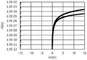
图34A和34B是说明实施例中的晶体管的电特性的图;34A and 34B are graphs illustrating electrical characteristics of transistors in an embodiment;
图35A和35B是说明实施例中的晶体管的电特性的图;35A and 35B are graphs illustrating electrical characteristics of transistors in an embodiment;
图36是说明实施例中的晶体管的GBT试验结果的图;36 is a graph illustrating GBT test results of transistors in the Examples;
图37A至37D是CAAC-OS的截面的Cs校正高分辨率TEM图像以及CAAC-OS的截面示意图;37A to 37D are Cs-corrected high-resolution TEM images of a cross-section of CAAC-OS and schematic cross-sections of CAAC-OS;
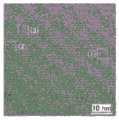
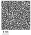
图38A至38D是CAAC-OS的平面的Cs校正高分辨率TEM图像;38A to 38D are Cs-corrected high-resolution TEM images of the plane of CAAC-OS;
图39A至39C是说明通过XRD得到的CAAC-OS及单晶氧化物半导体的结构分析结果的图;39A to 39C are diagrams illustrating the results of structural analysis of CAAC-OS and single crystal oxide semiconductor obtained by XRD;
图40A和40B是示出CAAC-OS的电子衍射图案的图;40A and 40B are graphs showing electron diffraction patterns of CAAC-OS;
图41是示出因电子照射导致的In-Ga-Zn氧化物的结晶部的变化的图。FIG. 41 is a graph showing changes in crystal parts of In-Ga-Zn oxide due to electron irradiation.
具体实施方式Detailed ways
下面将参照附图对实施方式进行说明。但是,实施方式可以以多种方式实施。所属技术领域的普通技术人员可以很容易地理解一个事实,就是其方式和详细内容可以在不脱离本发明的宗旨及其范围的条件下被变换为各种各样的形式。因此,本发明不应该被解释为仅限定于下面的实施方式的记载中。Embodiments will be described below with reference to the accompanying drawings. However, embodiments can be implemented in various ways. Those skilled in the art can easily understand the fact that the modes and details can be changed into various forms without departing from the spirit and scope of the present invention. Therefore, the present invention should not be construed as being limited only to the description of the following embodiments.
在附图中,为了清晰起见,有时夸大表示大小、层的厚度及区域。因此,本发明的实施方式并不一定限定于这种尺寸。此外,附图是示出理想例子的示意图,而本发明的实施方式不局限于附图所示的形状或数值。In the drawings, the size, thickness of layers, and regions are sometimes exaggerated for clarity. Therefore, embodiments of the present invention are not necessarily limited to such dimensions. In addition, the drawings are schematic diagrams showing ideal examples, and embodiments of the present invention are not limited to the shapes or numerical values shown in the drawings.
本说明书所使用的“第一”、“第二”、“第三”等序数词是为了避免构成要素的混淆而附加的,而不是为了在数目方面上进行限定的。The ordinal numbers such as "first", "second", and "third" used in this specification are added to avoid confusion among constituent elements, and are not intended to limit the number.
在本说明书中,为了方便起见,使用“上”、“下”等表示配置的词句以参照附图说明构成要素的位置关系。另外,构成要素的位置关系根据描述各构成要素的方向适当地改变。因此,不局限于本说明书中所说明的词句,根据情况可以适当地更换。In this specification, for the sake of convenience, words and phrases such as "upper" and "lower" that express arrangement are used to describe the positional relationship of the constituent elements with reference to the drawings. In addition, the positional relationship of the constituent elements is appropriately changed according to the direction in which each constituent element is described. Therefore, it is not limited to the words and phrases described in this specification, and can be appropriately replaced according to the situation.
在本说明书等中,晶体管是至少包括栅极、漏极以及源极这三个端子的元件。另外,晶体管在漏极(漏极端子、漏区或漏电极)与源极(源极端子、源区或源电极)之间具有沟道区域,并且电流能够流过漏极区域、沟道区域以及源极区域。注意,在本说明书等中,沟道区域是指电流主要流过的区域。In this specification and the like, a transistor is an element including at least three terminals of a gate, a drain, and a source. In addition, the transistor has a channel region between the drain (drain terminal, drain region or drain electrode) and the source (source terminal, source region or source electrode), and current can flow through the drain region, the channel region and source region. Note that in this specification and the like, the channel region refers to a region through which current mainly flows.
另外,例如当采用极性不同的晶体管或者在电路工作中电流方向变化时,源极及漏极的功能有可能互相调换。因此,在本说明书中,“源极”和“漏极”可以互相调换。In addition, for example, when transistors with different polarities are used or the direction of the current is changed during circuit operation, the functions of the source and the drain may be interchanged with each other. Therefore, in this specification, "source" and "drain" may be interchanged with each other.
在本说明书等中,“电连接”包括通过“具有某种电作用的元件”连接的情况。在此,“具有某种电作用的元件”只要可以进行连接对象间的电信号的授受,就对其没有特别的限制。例如,“具有某种电作用的元件”不仅包括电极和布线,而且还包括晶体管等的开关元件、电阻元件、电感器、电容元件、其他具有各种功能的元件等。In this specification and the like, "electrical connection" includes the case of being connected by "an element having a certain electrical effect". Here, the "element having a certain electrical effect" is not particularly limited as long as it can transmit and receive electrical signals between objects to be connected. For example, "an element having a certain electrical effect" includes not only electrodes and wirings, but also switching elements such as transistors, resistance elements, inductors, capacitance elements, and other elements having various functions.
在本说明书等中,“氧氮化硅膜”是指含氧量多于含氮量的膜,而“氮氧化硅膜”是指含氮量多于含氧量的膜。In this specification and the like, "silicon oxynitride film" refers to a film containing more oxygen than nitrogen, and "silicon oxynitride film" refers to a film containing more nitrogen than oxygen.
注意,在本说明书等中,当利用附图说明发明的结构时,表示相同的部分的符号在不同的附图中共同使用。Note that, in this specification and the like, when the configuration of the invention is described with reference to the drawings, the symbols representing the same parts are used in common in different drawings.
在本说明书等中,“平行”是指两条直线形成的角度为-10°以上且10°以下的状态。因此,也包括该角度为-5°以上且5°以下的状态。“大致平行”是指两条直线形成的角度为-30°以上且30°以下的状态。另外,“垂直”是指两条直线的角度为80°以上且100°以下的状态。因此,也包括该角度为85°以上且95°以下的状态。“大致垂直”是指两条直线形成的角度为60°以上且120°以下的状态。In the present specification and the like, "parallel" refers to a state in which the angle formed by two straight lines is -10° or more and 10° or less. Therefore, the state where this angle is -5° or more and 5° or less is also included. "Substantially parallel" refers to a state where the angle formed by the two straight lines is -30° or more and 30° or less. In addition, "perpendicular" refers to a state in which the angle between two straight lines is 80° or more and 100° or less. Therefore, the state where the angle is 85° or more and 95° or less is also included. "Substantially perpendicular" refers to a state where the angle formed by two straight lines is 60° or more and 120° or less.
实施方式1
在本实施方式中,参照图1A至1C、图2A至2C、图3A和3B、图4A至4C、图5A和5B、图6A至6C、图7A至7D、图8A至8D、图9A和9B、图10A至10D、图11A至11C、图12A和12B、图13A至13D、图14A和14B、图15A至15D、图16A至16D、图17A至17F、图18A至18F、以及图19A至19F说明本发明的一个方式的半导体装置。1A to 1C, FIGS. 2A to 2C, FIGS. 3A and 3B, FIGS. 4A to 4C, FIGS. 5A and 5B, FIGS. 6A to 6C, FIGS. 7A to 7D, FIGS. 8A to 8D, FIGS. 9B, Figures 10A to 10D, Figures 11A to 11C, Figures 12A and 12B, Figures 13A to 13D, Figures 14A and 14B, Figures 15A to 15D, Figures 16A to 16D, Figures 17A to 17F, Figures 18A to 18F, and Figure 19A A semiconductor device according to one embodiment of the present invention will be described through 19F.
〈半导体装置的结构实例1〉<Structure Example 1 of Semiconductor Device>
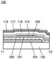
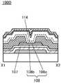
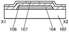
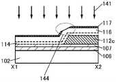
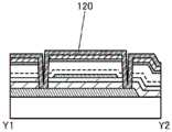
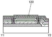
图1A是作为本发明的一个方式的半导体装置的晶体管100的俯视图,图1B相当于沿着图1A所示的点划线X1-X2的切断面的截面图,图1C相当于沿着图1A所示的点划线Y1-Y2的切断面的截面图。注意,在图1A中,为了方便起见,省略晶体管100的构成要素的一部分(用作栅极绝缘膜的绝缘膜等)。此外,有时将点划线X1-X2方向称为沟道长度方向,将点划线Y1-Y2方向称为沟道宽度方向。注意,有时在后面的晶体管的俯视图中也与图1A同样地省略构成要素的一部分。1A is a plan view of a
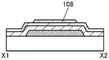
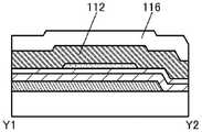
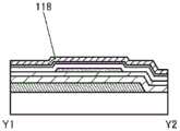
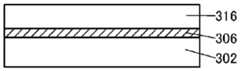
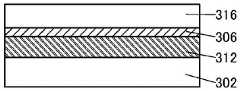
晶体管100包括:衬底102上的用作栅电极的导电膜104;衬底102及导电膜104上的绝缘膜106;绝缘膜106上的绝缘膜107;绝缘膜107上的氧化物半导体膜108;以及与氧化物半导体膜108电连接的用作源电极及漏电极的导电膜112a、112b。另外,在晶体管100上,详细地说,在导电膜112a、112b及氧化物半导体膜108上设置有绝缘膜114、116,并且在绝缘膜116上设置有保护膜117。另外,如图1B和1C所示那样,也可以采用在保护膜117上设置绝缘膜118的结构。The
另外,有时将绝缘膜106及绝缘膜107统称为第一绝缘膜,该第一绝缘膜具有晶体管100的栅极绝缘膜的功能。另外,有时将绝缘膜114及绝缘膜116统称为第二绝缘膜,该第二绝缘膜包含氧并具有对氧化物半导体膜108供应氧的功能。另外,绝缘膜118具有抑制杂质侵入到晶体管100中的保护绝缘膜的功能。In addition, the insulating
当在晶体管100所具有的氧化物半导体膜108中形成有氧空位时,产生作为载流子的电子,由此晶体管容易成为常开启特性。由此,为了获得稳定的晶体管特性,减少氧化物半导体膜108中的氧空位是重要的。本发明的一个方式的晶体管的结构特征在于:通过对氧化物半导体膜108上的绝缘膜,在此,氧化物半导体膜108上的绝缘膜114引入过剩氧,使氧从绝缘膜114移到氧化物半导体膜108中,来填补氧化物半导体膜108中的氧空位。此外,通过对氧化物半导体膜108上的绝缘膜116引入过剩氧,使氧从绝缘膜116经过绝缘膜114移到氧化物半导体膜108中,来填补氧化物半导体膜108中的氧空位。此外,晶体管的结构特征在于:通过对氧化物半导体膜108上的绝缘膜114及绝缘膜116引入过剩氧,使氧从绝缘膜114及绝缘膜116移到氧化物半导体膜108中,来填补氧化物半导体膜108中的氧空位。When oxygen vacancies are formed in the
另外,绝缘膜114、116更优选分别具有含有超过化学计量组成的氧的区域(氧过剩区域)。换句话说,绝缘膜114、116分别是一种能够释放氧的绝缘膜。此外,为了在绝缘膜114、116中分别设置氧过剩区域,例如,通过对沉积后的绝缘膜114、116经过保护膜117引入氧形成氧过剩区域。作为氧的引入方法,可以使用离子注入法、离子掺杂法、等离子体浸没式离子注入法、等离子体处理等。In addition, it is more preferable that the insulating
另外,绝缘膜114、116中的氧被释放,由于进行加热处理而扩散到氧化物半导体膜108中。例如,可以利用热脱附谱分析法(TDS:Thermal Desorption Spectroscopy)测量绝缘膜114、116中的氧分子的释放量。In addition, oxygen in the insulating
另一方面,绝缘膜114、116所包含的氧被释放,有时在晶体管100的制造工序中的加热处理时扩散到外部而不能有利地移动到氧化物半导体膜108中。但是,在本发明的一个方式的半导体装置中,在晶体管100上方,具体而言,在绝缘膜116上设置有保护膜117。保护膜117具有在引入氧时使氧透过且在进行加热处理时抑制氧的释放的功能。具体而言,保护膜117包含用于氧化物半导体膜108的金属元素中的至少一个。On the other hand, oxygen contained in the insulating
如上所述那样,通过在氧化物半导体膜108上设置绝缘膜114、116,可以使绝缘膜114、116中的氧移动到氧化物半导体膜108中,来填补形成在氧化物半导体膜108中的氧空位。另外,通过在绝缘膜116上设置具有抑制氧的释放的功能的保护膜117,可以抑制在晶体管100的制造工序中的加热处理时绝缘膜114、116中的氧被释放并扩散到外部。因此,可以有利地填补氧化物半导体膜108中的氧空位,由此可以提供可靠性得到提高的半导体装置。By providing the insulating
下面,对本实施方式的半导体装置所包括的其他构成要素进行详细的说明。Next, other constituent elements included in the semiconductor device of the present embodiment will be described in detail.
〈衬底〉<substrate>
对衬底102的材料的特性等没有特别的限制,只要该材料具有能够承受至少后续的加热处理的耐热性即可。例如,作为衬底102,可以使用玻璃衬底、陶瓷衬底、石英衬底、蓝宝石衬底等。另外,还可以使用以硅或碳化硅为材料的单晶半导体衬底或多晶半导体衬底、以硅锗等为材料的化合物半导体衬底、SOI(Silicon On Insulator:绝缘体上硅)衬底等用作衬底102。再者,也可以将设置有半导体元件的这些任何衬底可以用作衬底102。当作为衬底102使用玻璃衬底时,通过使用任何第6代(1500mm×1850mm)、第7代(1870mm×2200mm)、第8代(2200mm×2400mm)、第9代(2400mm×2800mm)、第10代(2950mm×3400mm)等尺寸的衬底。因而,可以制造大型显示装置。The properties and the like of the material of the
作为衬底102,也可以使用柔性衬底,并且在柔性衬底上直接形成晶体管100。或者,也可以在衬底102与晶体管100之间设置剥离层。剥离层可以在如下情况下使用,即在剥离层上制造半导体装置的一部分或全部,然后将其从衬底102分离并转置到其他衬底上的情况。此时,也可以将晶体管100转置到耐热性低的衬底或柔性衬底上。As the
〈导电膜〉<Conductive film>
用作栅电极的导电膜104及用作源电极及漏电极的导电膜112a、112b都可以使用选自铬(Cr)、铜(Cu)、铝(Al)、金(Au)、银(Ag)、锌(Zn)、钼(Mo)、钽(Ta)、钛(Ti)、钨(W)、锰(Mn)、镍(Ni)、铁(Fe)、钴(Co)中的金属元素、以上述任何金属元素为成分的合金或者组合上述任何金属元素的合金等形成。The
此外,导电膜104及导电膜112a、112b可以具有单层结构或者两层以上的叠层结构。例如,可以举出包含硅的铝膜的单层结构、在铝膜上层叠钛膜的两层结构、在氮化钛膜上层叠钛膜的两层结构、在氮化钛膜上层叠钨膜的两层结构、在氮化钽膜或氮化钨膜上层叠钨膜的两层结构以及依次层叠钛膜、铝膜和钛膜的三层结构等。另外,还可以使用组合铝与选自钛、钽、钨、钼、铬、钕、钪中的一种或多种而形成的合金膜或氮化物膜。In addition, the
导电膜104及导电膜112a、112b也可以使用铟锡氧化物、包含氧化钨的铟氧化物、包含氧化钨的铟锌氧化物、包含氧化钛的铟氧化物、包含氧化钛的铟锡氧化物、铟锌氧化物、添加有氧化硅的铟锡氧化物等透光导电材料。For the
另外,作为导电膜104及导电膜112a、112b,也可以应用Cu-X合金膜(X为Mn、Ni、Cr、Fe、Co、Mo、Ta或Ti)。通过使用Cu-X合金膜,可以通过湿蚀刻工序进行加工,从而可以抑制制造成本。In addition, as the
<栅极绝缘膜><Gate insulating film>
作为用作晶体管100的栅极绝缘膜的绝缘膜106、107,可以分别使用通过等离子体增强化学气相沉积(PECVD:Plasma Enhanced Chemical Vapor Deposition)法、溅射法等形成的包括氧化硅膜、氧氮化硅膜、氮氧化硅膜、氮化硅膜、氧化铝膜、氧化铪膜、氧化钇膜、氧化锆膜、氧化镓膜、氧化钽膜、氧化镁膜、氧化镧膜、氧化铈膜和氧化钕膜中的一种以上的绝缘层。注意,也可以使用选自上述材料中的单层或三层以上的绝缘膜,而不采用绝缘膜106、107的叠层结构。As the insulating
绝缘膜106具有抑制氧透过的阻挡膜的功能。例如,当对绝缘膜107、114、116及/或氧化物半导体膜108供应过剩氧时,绝缘膜106能够抑制氧透过。The insulating
接触于用作晶体管100的沟道区域的氧化物半导体膜108的绝缘膜107优选为氧化物绝缘膜,更优选包括包含超过化学计量组成的氧的区域(氧过剩区域)。换言之,绝缘膜107是能够释放氧的绝缘膜。为了在绝缘膜107中设置氧过剩区域,例如在氧气氛下形成绝缘膜107即可。或者,也可以对沉积后的绝缘膜107引入氧形成氧过剩区域。作为氧的引入方法,可以使用离子注入法、离子掺杂法、等离子体浸没式离子注入法、等离子体处理等。The insulating
此外,当作为绝缘膜107使用氧化铪时发挥如下效果。氧化铪的介电常数比氧化硅或氧氮化硅高。因此,可以使厚度比氧化硅大,由此,可以减少隧道电流引起的泄漏电流。也就是说,可以实现关态电流(off-state current)小的晶体管。再者,与包括非晶结构的氧化铪相比,包括结晶结构的氧化铪具有的介电常数高。因此,为了形成关态电流小的晶体管,优选使用包括结晶结构的氧化铪。作为结晶结构的一个例子,可以举出单斜晶系或立方晶系等。注意,本发明的一个方式不局限于此。Further, when hafnium oxide is used as the insulating
注意,在本实施方式中,作为绝缘膜106形成氮化硅膜,作为绝缘膜107形成氧化硅膜。与氧化硅膜相比,氮化硅膜的介电常数较高且为了得到与氧化硅膜相等的电容需要的厚度较大,因此,通过使晶体管100的栅极绝缘膜包括氮化硅膜,可以增加绝缘膜的物理厚度。因此,可以通过抑制晶体管100的绝缘耐压的下降并提高绝缘耐压来减少晶体管100的静电放电破坏。Note that, in this embodiment mode, a silicon nitride film is formed as the insulating
<氧化物半导体膜><Oxide semiconductor film>
氧化物半导体膜108具有In、Zn及M(M表示Ti、Ga、Y、Zr、Sn、La、Ce、Nd或Hf)。作为氧化物半导体膜108,典型地可以使用In-Ga氧化物、In-Zn氧化物、或In-M-Zn氧化物。尤其是,作为氧化物半导体膜108,优选使用In-M-Zn氧化物。The
当氧化物半导体膜108为In-M-Zn氧化物时,用来形成In-M-Zn氧化物的溅射靶材的金属元素的原子个数比优选满足In≥M及Zn≥M。这种溅射靶材的金属元素的原子个数比优选为In:M:Zn=1:1:1、In:M:Zn=1:1:1.2、In:M:Zn=3:1:2、In:M:Zn=4:2:4.1。另外,当氧化物半导体膜108为In-M-Zn氧化物时,作为溅射靶材优选使用包含多晶的In-M-Zn氧化物的靶材。通过使用包含多晶的In-M-Zn氧化物的靶材,容易形成具有结晶性的氧化物半导体膜108。注意,所形成的氧化物半导体膜108中的金属元素的原子个数比分别包含上述溅射靶材中的金属元素的原子个数比的±40%的范围内的误差。When the
另外,在氧化物半导体膜108为In-M-Zn氧化物的情况下,除了Zn及O之外的In和M的原子百分比优选为:In的原子百分比为25原子%以上,M的原子百分比低于75原子%,更优选为:In的原子百分比为34原子%以上,M的原子百分比低于66原子%。In addition, when the
氧化物半导体膜108的能隙为2eV以上,优选为2.5eV以上,更优选为3eV以上。如此,通过使用能隙较宽的氧化物半导体,可以降低晶体管100的关态电流。The energy gap of the
氧化物半导体膜108的厚度为3nm以上且200nm以下,优选为3nm以上且100nm以下,更优选为3nm以上且50nm以下。The thickness of the
作为氧化物半导体膜108使用载流子密度较低的氧化物半导体膜。例如,用作氧化物半导体膜108的氧化物半导体膜的载流子密度低于8×10¹¹/cm3,优选低于1×1011/cm3,更优选低于1×1010/cm3,且为1×10-9/cm3以上。As the
本发明不局限于上述记载的组成和材料,可以根据所需的晶体管的半导体特性及电特性(场效应迁移率、阈值电压等)来使用具有适当的组成的材料。另外,优选适当地设定氧化物半导体膜108的载流子密度、杂质浓度、缺陷密度、金属元素与氧的原子个数比、原子间距离、密度等,以得到所需的晶体管的半导体特性。The present invention is not limited to the compositions and materials described above, and materials having appropriate compositions can be used in accordance with desired semiconductor characteristics and electrical characteristics (field-effect mobility, threshold voltage, etc.) of the transistor. In addition, it is preferable to appropriately set the carrier density, impurity concentration, defect density, atomic ratio of metal element to oxygen, interatomic distance, density, etc. of the
注意,优选的是,通过作为氧化物半导体膜108使用杂质浓度低且缺陷态密度低的氧化物半导体膜,晶体管可以具有更优良的电特性。这里,将杂质浓度低且缺陷态密度低(氧空位的量少)的状态称为“高纯度本征”或“实质上高纯度本征”。因为高纯度本征或实质上高纯度本征的氧化物半导体膜的载流子发生源较少,所以可以具有低载流子密度。因此,在该氧化物半导体膜中形成有沟道区域的晶体管很少具有负阈值电压的电特性(很少具有常开启特性)。因为高纯度本征或实质上高纯度本征的氧化物半导体膜具有较低的缺陷态密度,所以有可能具有较少的载流子陷阱。此外,高纯度本征或实质上高纯度本征的氧化物半导体膜具有显著低的关态电流,即便元件具有1×106μm的沟道宽度W和10μm的沟道长度L,当源电极与漏电极间的电压(漏电压)在1V至10V的范围时,关态电流也可以半导体参数分析仪的测定极限以下,即1×10-13A以下。Note that it is preferable that the transistor can have more excellent electrical characteristics by using an oxide semiconductor film having a low impurity concentration and a low density of defect states as the
因此,在上述高纯度本征或实质上高纯度本征的氧化物半导体膜中形成有沟道区域的晶体管可以是电特性变动小且可靠性高的晶体管。此外,被氧化物半导体膜的陷阱能级俘获的电荷被释放需要较长的时间,有时像固定电荷那样动作。因此,有时在陷阱态密度高的氧化物半导体膜中形成有沟道区域的晶体管的电特性不稳定。作为杂质有氢、氮、碱金属及碱土金属等。Therefore, a transistor in which a channel region is formed in the high-purity intrinsic or substantially high-purity intrinsic oxide semiconductor film can be a transistor with little variation in electrical characteristics and high reliability. In addition, it takes a long time for the charges trapped in the trap levels of the oxide semiconductor film to be released, and sometimes behaves like fixed charges. Therefore, the electrical characteristics of a transistor in which a channel region is formed in an oxide semiconductor film having a high trap state density may be unstable. Examples of impurities include hydrogen, nitrogen, alkali metals and alkaline earth metals.
包含在氧化物半导体膜中的氢与键合于金属原子的氧起反应生成水,与此同时在发生氧脱离的晶格(或氧脱离的部分)中形成氧空位。由于氢进入该氧空位而有时生成作为载流子的电子。另外,有时由于氢的一部分与键合于金属原子的氧键合,产生作为载流子的电子。因此,使用包含氢的氧化物半导体膜的晶体管容易具有常开启特性。由此,优选尽可能减少氧化物半导体膜108中的氢。具体而言,在氧化物半导体膜108中,利用SIMS(二次离子质谱分析法:Secondary Ion Mass Spectrometry)测得的氢浓度为2×10²⁰atoms/cm3以下,优选为5×1019atoms/cm3以下,更优选为1×1019atoms/cm3以下,更优选为5×1018atoms/cm3以下,更优选为1×1018atoms/cm3以下,更优选为5×1017atoms/cm3以下,更优选为1×1016atoms/cm3以下。Hydrogen contained in the oxide semiconductor film reacts with oxygen bonded to metal atoms to generate water, and at the same time, oxygen vacancies are formed in the lattice (or the portion where oxygen detachment occurs) from which oxygen detachment occurs. Electrons are sometimes generated as carriers due to the entry of hydrogen into the oxygen vacancies. In addition, electrons as carriers may be generated due to the bonding of a part of hydrogen to oxygen bonded to metal atoms. Therefore, a transistor using an oxide semiconductor film containing hydrogen tends to have normally-on characteristics. Therefore, it is preferable to reduce hydrogen in the
当氧化物半导体膜108包含属于第14族元素之一的硅或碳时,在氧化物半导体膜108中氧空位增加,使得氧化物半导体膜108被n型化。因此,氧化物半导体膜108中的硅或碳的浓度(利用SIMS分析测得的浓度)或与氧化物半导体膜108之间的界面附近的硅或碳的浓度(利用SIMS分析测得的浓度)为2×10¹⁸atoms/cm3以下,优选为2×1017atoms/cm3以下。When the
另外,在氧化物半导体膜108中,利用SIMS分析测得的碱金属或碱土金属的浓度为1×10¹⁸atoms/cm3以下,优选为2×1016atoms/cm3以下。当碱金属及碱土金属与氧化物半导体键合时有时生成载流子而使晶体管的关态电流增大。由此,优选降低氧化物半导体膜108的碱金属或碱土金属的浓度。In addition, in the
当在氧化物半导体膜108中含有氮时,生成作为载流子的电子,载流子密度增加,使得氧化物半导体膜108容易被n型化。其结果是,使用含有氮的氧化物半导体膜的晶体管容易具有常开启特性。因此,优选尽可能地减少氧化物半导体膜中的氮,例如,利用SIMS分析测得的氮浓度优选为5×10¹⁸atoms/cm3以下。When nitrogen is contained in the
氧化物半导体膜108例如可以具有非单晶结构。非单晶结构例如包括下述CAAC-OS(C Axis Aligned Crystalline Oxide Semiconductor:c轴取向结晶氧化物半导体)、多晶结构、微晶结构或非晶结构。在非单晶结构中,非晶结构的缺陷态密度最高,而CAAC-OS的缺陷态密度最低。The
氧化物半导体膜108例如也可以具有非晶结构。非晶结构的氧化物半导体膜例如具有无秩序的原子排列且不具有结晶成分。或者,非晶结构的氧化物膜例如完全地具有非晶结构,而不具有结晶部。The
另外,氧化物半导体膜108也可以为具有非晶结构的区域、微晶结构的区域、多晶结构的区域、CAAC-OS的区域和单晶结构的区域中的两种以上的混合膜。例如混合膜有时具有单层结构,其中包括非晶结构的区域、微晶结构的区域、多晶结构的区域、CAAC-OS的区域和单晶结构的区域中的两种以上的区域。另外,混合膜有时具有非晶结构的区域、微晶结构的区域、多晶结构的区域、CAAC-OS的区域和单晶结构的区域中的两种以上的区域的叠层结构。In addition, the
<绝缘膜><Insulating film>
绝缘膜114、116都具有对氧化物半导体膜108供应氧的功能。绝缘膜118具有晶体管100的保护绝缘膜的功能。绝缘膜114、116包含氧。绝缘膜114是能够使氧透过的绝缘膜。注意,绝缘膜114还用作在后面形成绝缘膜116时缓和对氧化物半导体膜108造成的损伤的膜。Both the insulating
作为绝缘膜114,可以使用厚度为5nm以上且150nm以下,优选为5nm以上且50nm以下的氧化硅膜、氧氮化硅膜等。As the insulating
此外,优选使绝缘膜114中的缺陷量较少,典型的是,通过ESR(Electron SpinResonance:电子自旋共振)测量的起因于硅的悬空键的g=2.001处呈现的信号的自旋密度优选为3×10¹⁷自旋/cm3以下。这是因为若绝缘膜114的缺陷密度高,氧则与该缺陷键合,而使绝缘膜114中的氧透过量减少。In addition, the amount of defects in the insulating
注意,有时从外部进入绝缘膜114的氧不是全部移动到绝缘膜114的外部,而是其一部分残留在绝缘膜114的内部。另外,有时以氧进入绝缘膜114而在绝缘膜114中含有的氧移动到绝缘膜114的外部的方式在绝缘膜114中发生氧的移动。在形成能够使氧透过的氧化物绝缘膜作为绝缘膜114时,可以使从设置在绝缘膜114上的绝缘膜116脱离的氧经由绝缘膜114移动到氧化物半导体膜108。Note that oxygen that has entered the insulating
绝缘膜114可以使用因在氧化物半导体膜的价带顶的能量(Ev_os)和导带底的能量(Ec_os)之间的氮氧化物而态密度低的氧化物绝缘膜来形成。作为因在Ev_os和Ec_os之间的氮氧化物而态密度低的氧化物绝缘膜,可以使用氮氧化物的释放量少的氧氮化硅膜或氮氧化物的释放量少的氧氮化铝膜等。The insulating
此外,在热脱附谱分析中,氮氧化物的释放量少的氧氮化硅膜是氨释放量比氮氧化物的释放量多的膜,典型的是氨释放量为1×10¹⁸个/cm3以上且5×1019个/cm3以下。注意,该氨释放量为在进行膜表面温度为50℃以上且650℃以下,优选为50℃以上且550℃以下的加热处理时的释放量。In addition, in the thermal desorption spectrum analysis, a silicon oxynitride film with a small amount of nitrogen oxide released is a film with a larger amount of ammonia released than nitrogen oxides, and the amount of ammonia released is typically 1 × 10¹⁸ /cm3 or more and 5×10¹⁹ pieces/cm3 or less. Note that this ammonia release amount is the release amount when the film surface temperature is 50°C or higher and 650°C or lower, preferably 50°C or higher and 550°C or lower.
氮氧化物(NOx,x为0以上且2以下,优选为1以上且2以下),典型的是NO2或NO,在绝缘膜114等中形成能级。该能级位于氧化物半导体膜108的能隙中。由此,当氮氧化物被释放并扩散到绝缘膜114与氧化物半导体膜108的界面时,有时该能级在绝缘膜114一侧俘获电子。其结果,被俘获的电子留在绝缘膜114与氧化物半导体膜108的界面附近,由此使晶体管的阈值电压向正方向漂移。Nitrous oxide (NOx , where x is 0 or more and 2 or less, preferably 1 or more and 2 or less), typically NO2 or NO, forms an energy level in the insulating
另外,当进行加热处理时,氮氧化物与氨及氧起反应。当进行加热处理时,绝缘膜114所包含的氮氧化物与绝缘膜116所包含的氨起反应,由此绝缘膜114所包含的氮氧化物减少。因此,在绝缘膜114与氧化物半导体膜108之间的界面处不容易俘获电子。In addition, when heat treatment is performed, nitrogen oxides react with ammonia and oxygen. When the heat treatment is performed, the oxynitride contained in the insulating
绝缘膜114可以使用因氮氧化物而态密度低的氧化物绝缘膜而形成。注意,归因该氮氧化物的态密度有时可能会形成在氧化物半导体膜的价带顶的能量(Ev_os)和氧化物半导体膜的导带底的能量(Ec_os)之间。通过使用这种氧化物绝缘膜,可以降低晶体管的阈值电压的漂移,从而可以降低晶体管的电特性的变动。The insulating
通过进行晶体管的制造工序的加热处理,典型的是300℃以上且低于衬底的应变点的加热处理,在对绝缘膜114利用100K以下的ESR测得的光谱中,观察到g值为2.037以上且2.039以下的第一信号、g值为2.001以上且2.003以下的第二信号以及g值为1.964以上且1.966以下的第三信号。在X带的ESR测定中,第一信号与第二信号之间的分割宽度(splitwidth)及第二信号与第三信号之间的分割宽度大约为5mT。另外,g值为2.037以上且2.039以下的第一信号、g值为2.001以上且2.003以下的第二信号以及g值为1.964以上且1.966以下的第三信号的自旋密度的总和低于1×10¹⁸spins/cm3,典型为1×1017spins/cm3以上且低于1×1018spins/cm3。By performing the heat treatment in the manufacturing process of the transistor, typically at 300° C. or higher and lower than the strain point of the substrate, the g value was observed to be 2.037 in the spectrum measured by the ESR of 100 K or less for the insulating
在100K以下的ESR谱中,g值为2.037以上且2.039以下的第一信号、g值为2.001以上且2.003以下的第二信号以及g值为1.964以上且1.966以下的第三信号相当于起因于氮氧化物(NOx,x为0以上且2以下,优选为1以上且2以下)的信号。氮氧化物的典型例子包括一氧化氮、二氧化氮。就是说,g值为2.037以上且2.039以下的第一信号、g值为2.001以上且2.003以下的第二信号以及g值为1.964以上且1.966以下的第三信号的自旋密度的总数越少,氧化物绝缘膜中的氮氧化物含量越少。In the ESR spectrum of 100K or less, the first signal with a g value of 2.037 or more and 2.039 or less, the second signal with a g value of 2.001 or more and 2.003 or less, and the third signal with a g value of 1.964 or more and 1.966 or less correspond to A signal of nitrogen oxides (NOx , where x is 0 or more and 2 or less, preferably 1 or more and 2 or less). Typical examples of nitrogen oxides include nitrogen monoxide, nitrogen dioxide. That is, the smaller the total number of spin densities of the first signal with a g value of 2.037 or more and 2.039 or less, the second signal with a g value of 2.001 or more and 2.003 or less, and the third signal with a g value of 1.964 or more and 1.966 or less, The oxynitride content in the oxide insulating film is smaller.
另外,对因Ev_os与Ec_os之间的氮氧化物而态密度低的氧化物绝缘膜利用SIMS测得的氮浓度为6×10²⁰atoms/cm3以下。In addition, the nitrogen concentration of the oxide insulating film having a low density of states due to oxynitride between Ev_os and Ec_os was 6×10²⁰ atoms/cm3 or less as measured by SIMS.
通过在衬底温度为220℃以上、280℃以上或350℃以上的情况下利用使用硅烷及一氧化二氮的PECVD法形成Ev_os与Ec_os之间的氮氧化物的态密度低的氧化物绝缘膜,可以形成致密且硬度高的膜。An oxide with a low density of state of oxynitride between Ev_os and Ec_os is formed by PECVD using silane and nitrous oxide at a substrate temperature of 220° C. or higher, 280° C. or higher, or 350° C. or higher The insulating film can form a dense and high hardness film.
绝缘膜116使用其氧含量超过化学计量组成的氧化物绝缘膜形成。其氧含量超过化学计量组成的氧化物绝缘膜由于被加热而其一部分的氧脱离。通过TDS测量,其氧含量超过化学计量组成的氧化物绝缘膜换算为氧原子的氧的脱离量为1.0×10¹⁹atoms/cm3以上,优选为3.0×1020atoms/cm3以上。注意,上述TDS测量时的膜的表面温度优选为100℃以上且700℃以下或100℃以上且500℃以下。The insulating
作为绝缘膜116可以使用厚度为30nm以上且500nm以下,优选为50nm以上且400nm以下的氧化硅膜、氧氮化硅膜等。As the insulating
此外,优选使绝缘膜116中的缺陷量较少,典型的是,通过ESR测量的起因于硅的悬空键的g=2.001处呈现的信号的自旋密度低于1.5×10¹⁸自旋/cm3,更优选为1×1018自旋/cm3以下。由于绝缘膜116与绝缘膜114相比离氧化物半导体膜108更远,所以绝缘膜116的缺陷密度也可以高于绝缘膜114。In addition, the amount of defects in the insulating
另外,因为绝缘膜114、116可以使用相同种类材料形成,所以有时无法明确地确认到绝缘膜114与绝缘膜116之间的界面。因此,在本实施方式中,以虚线图示出绝缘膜114与绝缘膜116之间的界面。注意,虽然在本实施方式中说明绝缘膜114与绝缘膜116的两层结构,但是本发明不局限于此,例如,也可以采用绝缘膜114的单层结构。In addition, since the insulating
绝缘膜118包含氮。另外,绝缘膜118包含氮及硅。此外,绝缘膜118具有能够阻挡氧、氢、水、碱金属、碱土金属等的功能。通过设置绝缘膜118,能够防止氧从氧化物半导体膜108释放并扩散到外部,并且能够防止绝缘膜114、116所包含的氧被释放并扩散到外部,还能够抑制氢、水等从外部侵入氧化物半导体膜108中。作为绝缘膜118,例如可以使用氮化物绝缘膜。作为该氮化物绝缘膜,有氮化硅、氮氧化硅、氮化铝、氮氧化铝等。另外,也可以设置对氧、氢、水等具有阻挡效果的氧化物绝缘膜代替对氧、氢、水、碱金属、碱土金属等具有阻挡效果的氮化物绝缘膜。作为对氧、氢、水等具有阻挡效果的氧化物绝缘膜,有氧化铝膜、氧氮化铝膜、氧化镓膜、氧氮化镓膜、氧化钇膜、氧氮化钇膜、氧化铪膜、氧氮化铪膜等。The insulating
<保护膜><Protective film>
保护膜117包含用于氧化物半导体膜108的金属元素中的至少一个。例如,在氧化物半导体膜108包含In、Zn及M(M表示Ti、Ga、Sn、Y、Zr、La、Ce、Nd或Hf)的情况下,保护膜117包含In、Zn、Ti、Ga、Sn、Y、Zr、La、Ce、Nd或Hf中的至少一个元素。尤其是,作为保护膜117优选使用In-Sn氧化物、In-Zn氧化物、In-Ga氧化物、Zn氧化物、Al-Zn氧化物或In-Ga-Zn氧化物。The
当作为氧化物半导体膜108使用In-Ga-Zn氧化物时,保护膜117优选至少包含Ga。另外,当作为氧化物半导体膜108使用In-Ga-Zn氧化物时,保护膜117优选至少包含Zn。另外,当作为氧化物半导体膜108使用In-Ga-Zn氧化物时,保护膜117优选至少包含Ga和Zn。When In-Ga-Zn oxide is used as the
当保护膜117的厚度薄时,抑制氧的释放的功能可能降低。另一方面,当保护膜117的厚度厚时,在氧添加处理时氧不容易穿过保护膜117。因此,保护膜117的厚度为3nm以上且30nm以下,优选为5nm以上且15nm以下。另外,保护膜117优选具有结晶性。例如,当作为保护膜117使用In-Ga-Zn氧化物且该In-Ga-Zn氧化物是下面说明的CAAC-OS膜时,可以优选地抑制添加到绝缘膜116中的氧的释放。另外,保护膜117的电阻率优选高。当保护膜117的电阻率低时,在保护膜117和导电膜112a、112b之间有时形成寄生电容。保护膜117的电阻率例如可以为1010Ωcm以上且低于1018Ωcm。When the thickness of the
虽然上述所记载的导电膜、绝缘膜、保护膜及氧化物半导体膜等各种膜可以利用溅射法或PECVD法形成,但是也可以利用例如热CVD(Thermaml Chemical VaporDeposition:热化学气相沉积)法或ALD(Atomic Layer Deposition:原子层沉积)法形成。作为热CVD法的例子,可以举出MOCVD(Metal Organic Chemical Vapor Deposition:金属有机化学气相沉积)法。Various films such as the conductive film, insulating film, protective film, and oxide semiconductor film described above can be formed by sputtering or PECVD, but can also be formed by, for example, thermal CVD (Thermaml Chemical Vapor Deposition: Thermal Chemical Vapor Deposition) Or ALD (Atomic Layer Deposition: Atomic Layer Deposition) method. As an example of a thermal CVD method, MOCVD (Metal Organic Chemical Vapor Deposition: Metal Organic Chemical Vapor Deposition) method is mentioned.
由于热CVD法是不使用等离子体的成膜方法,因此具有不产生因等离子体损伤所引起的缺陷的优点。Since the thermal CVD method is a film formation method that does not use plasma, it has an advantage that defects due to plasma damage do not occur.
可以以如下方法进行利用热CVD法的沉积:将源气体及氧化剂同时供应到处理室内,将处理室内的压力设定为大气压或减压,使其在衬底附近或在衬底上发生反应。Deposition by thermal CVD can be performed by supplying a source gas and an oxidizing agent simultaneously into a processing chamber, setting the pressure in the processing chamber to atmospheric pressure or reduced pressure, and causing a reaction near or on the substrate.
另外,也可以以如下方法进行利用ALD法的沉积:将处理室内的压力设定为大气压或减压,将用于反应的源气体依次引入处理室,并且按该顺序反复地引入气体。例如,通过切换各开关阀(也称为高速阀)来将两种以上的源气体依次供应到处理室内。为了防止多种源气体混合,例如,在引入第一源气体的同时或之后引入惰性气体(氩或氮等)等,然后引入第二源气体。注意,当同时引入第一源气体及惰性气体时,惰性气体被用作载气,另外,可以在引入第二源气体的同时引入惰性气体。另外,也可以不引入惰性气体而通过真空抽气将第一源气体排出,然后引入第二源气体。第一源气体附着到衬底表面形成第一层,之后引入的第二源气体与该第一层起反应,由此第二层层叠在第一层上而形成薄膜。通过按该顺序反复多次地引入气体直到获得所希望的厚度为止,可以形成台阶覆盖性良好的薄膜。由于薄膜的厚度可以根据按顺序反复引入气体的次数来进行调节,因此,ALD法可以准确地调节厚度而适用于制造微型FET。Alternatively, deposition by the ALD method may be performed by setting the pressure in the processing chamber to atmospheric pressure or reduced pressure, sequentially introducing the source gas for the reaction into the processing chamber, and repeating the introduction of the gas in this order. For example, by switching each on-off valve (also referred to as a high-speed valve), two or more source gases are sequentially supplied into the processing chamber. In order to prevent mixing of various source gases, for example, an inert gas (argon, nitrogen, etc.) or the like is introduced at the same time as or after the introduction of the first source gas, and then the second source gas is introduced. Note that when the first source gas and the inert gas are introduced at the same time, the inert gas is used as the carrier gas, and in addition, the inert gas may be introduced simultaneously with the introduction of the second source gas. Alternatively, the first source gas may be exhausted by vacuum evacuation without introducing the inert gas, and then the second source gas may be introduced. The first source gas is attached to the surface of the substrate to form a first layer, and the second source gas introduced thereafter reacts with the first layer, whereby the second layer is laminated on the first layer to form a thin film. By repeatedly introducing gas in this order until a desired thickness is obtained, a thin film with good step coverage can be formed. Since the thickness of the thin film can be adjusted according to the number of repeated introduction of the gas in sequence, the ALD method can accurately adjust the thickness and is suitable for the fabrication of micro-FETs.
通过MOCVD法等热CVD法可以形成上述导电膜、绝缘膜、氧化物半导体膜等各种膜,例如,当形成In-Ga-Zn-O膜时,使用三甲基铟、三甲基镓及二甲基锌。三甲基铟的化学式为In(CH3)3。三甲基镓的化学式为Ga(CH3)3。另外,二甲基锌的化学式为Zn(CH3)2。另外,不局限于上述组合,也可以使用三乙基镓(化学式为Ga(C2H5)3)代替三甲基镓,并使用二乙基锌(化学式为Zn(C2H5)2)代替二甲基锌。Various films such as the conductive film, insulating film, and oxide semiconductor film described above can be formed by thermal CVD such as MOCVD. For example, when forming an In-Ga-Zn-O film, trimethyl indium, trimethyl gallium and Dimethyl zinc. The chemical formula of trimethylindium is In(CH3 )3 . The chemical formula of trimethylgallium is Ga(CH3 )3 . In addition, the chemical formula of dimethyl zinc is Zn(CH3 )2 . In addition, not limited to the above combination, triethylgallium (chemical formula Ga(C2 H5 )3 ) may be used instead of trimethylgallium, and diethylzinc (chemical formula Zn(C2 H5 )2 ) instead of dimethylzinc.
例如,在使用利用ALD法的沉积装置形成氧化铪膜时,使用如下两种气体:通过使包含溶剂和铪前体化合物的液体(铪醇盐、四二甲基酰胺铪(TDMAH)等铪酰胺)气化而得到的源气体;以及用作氧化剂的臭氧(O3)。此外,四二甲基酰胺铪的化学式为Hf[N(CH3)2]4。另外,作为其它材料液有四(乙基甲基酰胺)铪等。For example, when forming a hafnium oxide film using a deposition apparatus using the ALD method, two gases are used. ) gasified source gas; and ozone (O3 ) used as an oxidant. In addition, the chemical formula of hafnium tetradimethylamide is Hf[N(CH3 )2 ]4 . In addition, tetrakis(ethylmethylamide) hafnium etc. are mentioned as another material liquid.
例如,在使用利用ALD法的沉积装置形成氧化铝膜时,使用如下两种气体:用作氧化剂的H2O;以及通过使包含溶剂和铝前体化合物的液体(三甲基铝(TMA)等)气化而得到的源气体。此外,三甲基铝的化学式为Al(CH3)3。另外,作为其它材料液有三(二甲基酰胺)铝、三异丁基铝、三(2,2,6,6-四甲基-3,5-庚二酮)铝。For example, when an aluminum oxide film is formed using a deposition apparatus utilizing the ALD method, two gases are used: H2 O used as an oxidant; and a liquid (trimethylaluminum (TMA) containing a solvent and an aluminum precursor compound) is used etc.) source gas obtained by gasification. In addition, the chemical formula of trimethylaluminum is Al(CH3 )3 . In addition, as other material liquids, there are tris(dimethylamide)aluminum, triisobutylaluminum, and tris(2,2,6,6-tetramethyl-3,5-heptanedione)aluminum.
例如,在使用利用ALD法的沉积装置形成氧化硅膜时,使六氯乙硅烷附着在被成膜面上,去除附着物所包含的氯,供应氧化性气体(O2、一氧化二氮)的自由基使其与附着物起反应。For example, when a silicon oxide film is formed using a deposition apparatus using the ALD method, hexachlorodisilane is adhered to the film-forming surface, chlorine contained in the adherend is removed, and oxidizing gas (O2 , nitrous oxide) is supplied. free radicals to react with attachments.
例如,在使用利用ALD法的沉积装置形成钨膜时,依次多次引入WF6气体和B2H6气体形成初始钨膜,然后依次多次引入WF6气体和H2气体形成钨膜。注意,也可以使用SiH4气体代替B2H6气体。For example, when forming a tungsten film using an ALD deposition apparatus,WF6 gas andB2H6 gas are sequentially introduced multiple times to form an initial tungsten film, and thenWF6 gas andH2gas are sequentially introduced multiple times to form a tungsten film. Note that SiH4 gas may also be used instead of B2 H6 gas.
例如,在使用利用ALD法的沉积装置形成氧化物半导体膜如In-Ga-ZnO膜时,连续地多次引入In(CH3)3气体和O3气体形成In-O层,然后引入Ga(CH3)3气体和O3气体形成GaO层,之后连续地多次引入Zn(CH3)2气体和O3气体形成ZnO层。注意,这些层的顺序不局限于上述例子。此外,也可以混合这些气体来形成混合化合物层如In-Ga-O层、In-Zn-O层、Ga-Zn-O层等。注意,虽然也可以使用利用Ar等惰性气体进行鼓泡而得到的H2O气体代替O3气体,但是优选使用不包含H的O3气体。另外,也可以使用In(C2H5)3气体代替In(CH3)3气体。也可以使用Ga(C2H5)3气体代替Ga(CH3)3气体。也可以使用Zn(CH3)2气体。For example, when an oxide semiconductor film such as an In-Ga-ZnO film is formed using a deposition apparatus utilizing the ALD method, In(CH3 )3 gas and O3 gas are successively introduced multiple times to form an In-O layer, and then Ga( CH3 )3 gas and O3 gas form a GaO layer, and then Zn(CH3 )2 gas and O3 gas are continuously introduced multiple times to form a ZnO layer. Note that the order of these layers is not limited to the above example. In addition, these gases may also be mixed to form mixed compound layers such as In-Ga-O layers, In-Zn-O layers, Ga-Zn-O layers, and the like. Note that H2 O gas bubbling with an inert gas such as Ar may be used instead of O3 gas, but O3 gas not containing H is preferably used. In addition, In(C2 H5 )3 gas may be used instead of In(CH3 )3 gas. Instead of Ga(CH3 )3 gas, Ga(C2 H5 )3 gas may also be used. Zn(CH3 )2 gas can also be used.
〈半导体装置的结构实例2〉<Structure Example 2 of Semiconductor Device>
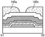
接着,参照图2A至2C说明与图1A至1C所示的晶体管100不同的结构实例。另外,当表示具有与上面所说明的功能相同的功能的部分时有时使用相同的阴影线,而不特别附加附图标记。Next, structural examples different from those of the
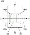
图2A是作为本发明的一个方式的半导体装置的晶体管150的俯视图,图2B相当于沿着图2A所示的点划线X1-X2的切断面的截面图,图2C相当于沿着图2A所示的点划线Y1-Y2的切断面的截面图。2A is a plan view of a
晶体管150包括:衬底102上的用作栅电极的导电膜104;衬底102及导电膜104上的绝缘膜106;绝缘膜106上的绝缘膜107;绝缘膜107上的氧化物半导体膜108;氧化物半导体膜108上的绝缘膜114;绝缘膜114上的绝缘膜116;以及通过设置在绝缘膜114及绝缘膜116中的开口部141a、141b与氧化物半导体膜108电连接的用作源电极及漏电极的导电膜112a、112b。另外,在晶体管150上,详细地说,在导电膜112a、112b及绝缘膜116上设置有保护膜117。另外,如图2B和2C所示那样,也可以在保护膜117上设置绝缘膜118。The
晶体管100采用沟道蚀刻型结构,而图2A、2B及2C所示的晶体管150采用沟道保护型结构。如此,本发明的一个方式的半导体装置可以采用沟道蚀刻型结构及沟道保护型结构中的任一个。The
晶体管150与上面所示的晶体管100同样地具有氧化物半导体膜108上的绝缘膜114、116,由此绝缘膜114、116所包含的氧可以填补氧化物半导体膜108中的氧空位。另外,通过在绝缘膜116上设置具有抑制氧的释放的功能的保护膜117,可以抑制在晶体管150的制造工序中的加热处理时绝缘膜114、116中的氧被释放并扩散到外部。因此,可以适当地填补氧化物半导体膜108中的氧空位,可以提供可靠性得到提高的半导体装置。The
〈半导体装置的结构实例3〉<Structure Example 3 of Semiconductor Device>
接着,参照图3A和3B说明与图2A至2C所示的晶体管150不同的结构实例。另外,当表示具有与上面所说明的功能相同的功能的部分时有时使用相同的阴影线,而不特别附加附图标记。Next, structural examples different from those of the
图3A是晶体管150A的沟道长度方向的截面图,图3B是晶体管150A的沟道宽度方向的截面图。注意,晶体管150A的俯视图与图2A所示的俯视图相似,所以在此省略其记载。3A is a cross-sectional view in the channel length direction of the
图3A和3B所示的晶体管150A包括:衬底102上的用作栅电极的导电膜104;衬底102及导电膜104上的绝缘膜106;绝缘膜106上的绝缘膜107;绝缘膜107上的氧化物半导体膜108;氧化物半导体膜108上的绝缘膜114;绝缘膜114上的绝缘膜116;绝缘膜116上的保护膜117;以及通过形成在绝缘膜114、绝缘膜116、保护膜117中的开口部141a、141b与氧化物半导体膜108电连接的用作源电极及漏电极的导电膜112a、112b。另外,如图3A和3B所示那样,也可以采用在晶体管150A上,详细地说,在导电膜112a、112b及保护膜117上设置绝缘膜118的结构。The
晶体管150A在设置有保护膜117之处与图2B及2C所示的晶体管150不同。其他结构与晶体管150同样,并且发挥同样的效果。The
〈半导体装置的结构实例4〉<Structure Example 4 of Semiconductor Device>
接着,参照图4A至4C说明与图2A至2C所示的晶体管150不同的结构实例。另外,当表示具有与上面所说明的功能相同的功能的部分时有时使用相同的阴影线,而不特别附加附图标记。Next, structural examples different from those of the
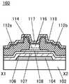
图4A是作为本发明的一个方式的半导体装置的晶体管160的俯视图,图4B相当于沿着图4A所示的点划线X1-X2的切断面的截面图,图4C相当于沿着图4A所示的点划线Y1-Y2的切断面的截面图。4A is a plan view of a
晶体管160包括:衬底102上的用作栅电极的导电膜104;衬底102及导电膜104上的绝缘膜106;绝缘膜106上的绝缘膜107;绝缘膜107上的氧化物半导体膜108;氧化物半导体膜108上的绝缘膜114;绝缘膜114上的绝缘膜116;以及与氧化物半导体膜108电连接的用作源电极及漏电极的导电膜112a、112b。另外,在晶体管160上,详细地说,在导电膜112a、112b及绝缘膜116上设置有保护膜117。另外,如图4B和4C所示那样,也可以采用在晶体管160上,详细地说,在导电膜112a、112b及保护膜117上设置绝缘膜118的结构。The
晶体管160与图2A至2C所示的晶体管150的不同之处在于绝缘膜114、116的形状。具体而言,晶体管160的绝缘膜114、116以岛状设置在氧化物半导体膜108的沟道区域上。其他结构与晶体管150同样,并且发挥同样的效果。The
〈半导体装置的结构实例5〉<Structure Example 5 of Semiconductor Device>
接着,参照图5A及5B说明与图4A至4C所示的晶体管160不同的结构实例。另外,当表示具有与上面所说明的功能相同的功能的部分时有时使用相同的阴影线,而不特别附加附图标记。Next, structural examples different from those of the
图5A是晶体管160A的沟道长度方向的截面图,图5B是晶体管160A的沟道宽度方向的截面图。注意,晶体管160A的俯视图与图4A所示的俯视图相似,所以在此省略其记载。5A is a cross-sectional view in the channel length direction of the
晶体管160A包括:衬底102上的用作栅电极的导电膜104;衬底102及导电膜104上的绝缘膜106;绝缘膜106上的绝缘膜107;绝缘膜107上的氧化物半导体膜108;氧化物半导体膜108上的绝缘膜114;绝缘膜114上的绝缘膜116;绝缘膜116上的保护膜117;以及与氧化物半导体膜108电连接的用作源电极及漏电极的导电膜112a、112b。另外,如图5A和5B所示那样,也可以采用在晶体管160A上,详细地说,在导电膜112a、112b及保护膜117上设置绝缘膜118的结构。
晶体管160A在设置有保护膜117之处与图4B和4C所示的晶体管160不同。其他结构与晶体管160同样,并且发挥同样的效果。The
〈半导体装置的结构实例6〉<Structure Example 6 of Semiconductor Device>
接着,参照图6A至6C说明与图1A至1C所示的晶体管100不同的结构实例。另外,当表示具有与上面所说明的功能相同的功能的部分时有时使用相同的阴影线,而不特别附加附图标记。Next, structural examples different from those of the
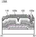
图6A是作为本发明的一个方式的半导体装置的晶体管170的俯视图,图6B相当于沿着图6A所示的点划线X1-X2的切断面的截面图,图6C相当于沿着图6A所示的点划线Y1-Y2的切断面的截面图。6A is a plan view of a
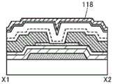
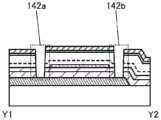
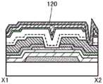
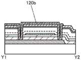
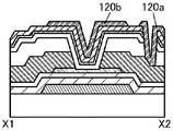
晶体管170包括:衬底102上的用作栅电极的导电膜104;衬底102及导电膜104上的绝缘膜106;绝缘膜106上的绝缘膜107;绝缘膜107上的氧化物半导体膜108;与氧化物半导体膜108电连接的用作源电极及漏电极的导电膜112a、112b;氧化物半导体膜108、导电膜112a、112b上的绝缘膜114;绝缘膜114上的绝缘膜116;绝缘膜116上的保护膜117;保护膜117上的绝缘膜118;以及绝缘膜118上的导电膜120a、120b。另外,导电膜120a通过形成在绝缘膜114、116、绝缘膜118、保护膜117中的开口部142c与导电膜112b连接。另外,导电膜120b形成在绝缘膜118上的与氧化物半导体膜108重叠的位置上。The
在晶体管170中,绝缘膜114、116、118及保护膜117被用作晶体管170的第二栅极绝缘膜。在晶体管170中,导电膜120a例如具有用作用于显示装置的像素电极的功能。在晶体管170中,导电膜120b被用作第二栅电极(也称为背栅电极)。In the
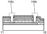
如图6C所示,导电膜120b通过设置于绝缘膜106、107、114、116、118及保护膜117中的开口部142a、142b中连接于用作栅电极的导电膜104。因此,对导电膜120b和导电膜104施加相同的电位。As shown in FIG. 6C , the
另外,在本实施方式中例示出设置开口部142a、142b使导电膜120b与导电膜104连接的结构,但是本发明的有一个方式不局限于此。例如,也可以采用仅形成开口部142a和开口部142b中的任一个而使导电膜120b与导电膜104连接的结构,或者,不设置开口部142a和开口部142b而不使导电膜120b与导电膜104连接的结构。当不使导电膜120b与导电膜104连接时,可以对导电膜120b和导电膜104施加不同的电位。In addition, in the present embodiment, the configuration in which the
如图6B所示,氧化物半导体膜108位于与用作栅电极的导电膜104及用作第二栅电极的导电膜120b相对的位置,夹在两个用作栅电极的导电膜之间。用作第二栅电极的导电膜120b的沟道长度方向的长度及沟道宽度方向的长度都大于氧化物半导体膜108的沟道长度方向的长度及沟道宽度方向的长度。导电膜120b隔着绝缘膜114、116、118及保护膜117覆盖整个氧化物半导体膜108。此外,由于用作第二栅电极的导电膜120b与用作栅电极的导电膜104在设置于绝缘膜106、107、114、116、118及保护膜117中的开口部142a、142b中连接,所以氧化物半导体膜108的沟道宽度方向的侧面隔着绝缘膜114、116、118及保护膜117与用作第二栅电极的导电膜120b相对。As shown in FIG. 6B , the
换言之,在晶体管170的沟道宽度方向上,用作栅电极的导电膜104及用作第二栅电极的导电膜120b通过设置于用作栅极绝缘膜的绝缘膜106、107及用作第二栅极绝缘膜的绝缘膜114、116、118及保护膜117中的开口部连接,同时导电膜104及导电膜120b隔着用作栅极绝缘膜的绝缘膜106、107及用作第二栅极绝缘膜的绝缘膜114、116、118及保护膜117围绕氧化物半导体膜108。In other words, in the channel width direction of the
上述结构能够利用用作栅电极的导电膜104及用作第二栅电极的导电膜120b的电场电围绕晶体管170所包括的氧化物半导体膜108。如晶体管170所示,可以将利用栅电极及第二栅电极的电场电围绕形成有沟道区域的氧化物半导体膜的晶体管的装置结构称为围绕的沟道(s-沟道)结构。The above-described structure can electrically surround the
因为晶体管170具有s-沟道结构,所以可以使用用作栅电极的导电膜104对氧化物半导体膜108有效地施加用来引起沟道的电场。由此,晶体管170的电流驱动能力得到提高,从而可以得到高的通态电流(on-state current)特性。此外,由于可以增加通态电流,所以可以使晶体管170的尺寸缩小。另外,由于晶体管170具有被用作栅电极的导电膜104及用作第二栅电极的导电膜120b围绕的结构,所以可以提高晶体管170的机械强度。Since the
其他结构与图1A至1C所示的晶体管100同样,并且发挥与晶体管100同样的效果。The other structures are the same as those of the
〈半导体装置的结构实例7〉<Structure Example 7 of Semiconductor Device>
接着,参照图7A至7D说明与图6A至6C所示的晶体管170不同的结构实例。另外,当表示具有与上面所说明的功能相同的功能的部分时有时使用相同的阴影线,而不特别附加附图标记。Next, structural examples different from those of the
图7A是晶体管170A的沟道长度方向的截面图,图7B是晶体管170A的沟道宽度方向的截面图。图7C是晶体管170B的沟道长度方向的截面图,图7D是晶体管170B的沟道宽度方向的截面图。注意,晶体管170A及晶体管170B的俯视图与图6A所示的俯视图相似,所以在此省略其记载。另外,当表示具有与上面所说明的功能相同的功能的部分时有时使用相同的阴影线,而不特别附加附图标记。7A is a cross-sectional view in the channel length direction of the
图7A和7B都是图6B和6C所示的晶体管170的变形例的截面图。图7C和7D都是图6B和6C所示的晶体管170的变形例的截面图。7A and 7B are each a cross-sectional view of a modification of the
在图7A和7B所示的晶体管170A中,在图6B和6C所示的晶体管170上,具体地说,在绝缘膜118及导电膜120a、120b上设置有绝缘膜122的结构。In the
可以使用与能够用于绝缘膜118的材料相似的材料形成绝缘膜122。另外,以覆盖导电膜120b且使导电膜120a的一部分露出的方式设置绝缘膜122,即可。通过设置绝缘膜122,可以保护导电膜120b,可以制造可靠性得到提高的半导体装置。The insulating
图7C和7D所示的晶体管170B与图6B和6C所示的晶体管170的不同之处是绝缘膜114、116、118、保护膜117的层叠顺序。另外,因为层叠顺序不同,所以图7C和7D中的绝缘膜114、116、118、保护膜117及导电膜120a、120b的形状不同与图6B和6C中的。The
另外,如图7C所示那样,晶体管170B的绝缘膜116设置在导电膜112a、112b上。通过形成如图7C所示的绝缘膜116的形状,可以减少导电膜112a与导电膜120b之间的寄生电容、导电膜112b与导电膜120b之间的寄生电容。另外,因为在氧化物半导体膜108的沟道区域中不形成绝缘膜116,所以可以减薄第二栅极绝缘膜的膜厚度。In addition, as shown in FIG. 7C , the insulating
另外,晶体管170B的绝缘膜114设置在绝缘膜116及氧化物半导体膜108上。另外,保护膜117设置在绝缘膜114上。另外,绝缘膜118设置在保护膜117上。另外,导电膜120a、120b设置在绝缘膜118上。另外,绝缘膜114、保护膜117及绝缘膜118具有晶体管170B的第二栅极绝缘膜的功能。In addition, the insulating
晶体管170A及晶体管170B的其他结构与晶体管170同样,并且发挥与晶体管170同样的效果。The other structures of the
〈半导体装置的结构实例8〉<Structure Example 8 of Semiconductor Device>
接着,参照图8A至8D说明与图1A至1C所示的晶体管100不同的结构实例。另外,当表示具有与上面所说明的功能相同的功能的部分时有时使用相同的阴影线,而不特别附加附图标记。Next, structural examples different from those of the
图8A和8B都是图1B和1C所示的晶体管100的变形例的截面图。图8C和8D都是图1B和1C所示的晶体管100的变形例的截面图。8A and 8B are each a cross-sectional view of a modification of the
除了氧化物半导体膜108具有三层结构之外,图8A和8B所示的晶体管100C具有与图1B和1C所示的晶体管100相同的结构。更具体地说,晶体管100C所具有的氧化物半导体膜108具有氧化物半导体膜108a、氧化物半导体膜108b以及氧化物半导体膜108c。另外,除了氧化物半导体膜108具有两层结构之外,图8C和8D所示的晶体管100D具有与图1B和1C所示的晶体管100相同的结构。更具体地说,晶体管100D所具有的氧化物半导体膜108具有氧化物半导体膜108b及氧化物半导体膜108c。The
在此,参照图9A和9B说明包括氧化物半导体膜108a、108b、108c、以及接触于氧化物半导体膜108b、108c的绝缘膜的能带结构。Here, the energy band structure including the
图9A是包括绝缘膜107、氧化物半导体膜108a、108b、108c以及绝缘膜114的叠层的膜厚方向的能带结构的一个例子。另外,图9B是包括绝缘膜107、氧化物半导体膜108b、108c以及绝缘膜114的叠层的膜厚方向的能带结构的一个例子。在能带结构中,为了容易理解,分别示出绝缘膜107、氧化物半导体膜108a、108b、108c及绝缘膜114的导带底的能级(Ec)。9A is an example of the energy band structure in the film thickness direction of the stack including the insulating
在图9A的能带图中,使用氧化硅膜作为绝缘膜107、114,使用利用金属元素的原子个数比为In:Ga:Zn=1:3:2的金属氧化物靶材而形成的氧化物半导体膜作为氧化物半导体膜108a,使用利用金属元素的原子个数比为In:Ga:Zn=1:1:1的金属氧化物靶材而形成的氧化物半导体膜作为氧化物半导体膜108b,使用利用金属元素的原子个数比为In:Ga:Zn=1:3:2的金属氧化物靶材而形成的氧化物半导体膜作为氧化物半导体膜108c。In the energy band diagram of FIG. 9A , silicon oxide films are used as the insulating
在图9B的能带图中,使用氧化硅膜作为绝缘膜107、114,使用利用金属元素的原子个数比为In:Ga:Zn=1:1:1的金属氧化物靶材而形成的氧化物半导体膜作为氧化物半导体膜108b,使用利用金属元素的原子个数比为In:Ga:Zn=1:3:2的金属氧化物靶材而形成的金属氧化膜作为氧化物半导体膜108c。In the energy band diagram of FIG. 9B , silicon oxide films are used as insulating
如图9A和9B所示,在氧化物半导体膜108a与氧化物半导体膜108b之间及氧化物半导体膜108b与氧化物半导体膜108c之间,导带底的能级平缓地变化。也可以说导带底的能级连续地变化或连续接合。为了实现这样的能带结构,优选不使在氧化物半导体膜108a与氧化物半导体膜108b之间的界面或在氧化物半导体膜108b与氧化物半导体膜108c之间的界面存在杂质,该杂质会形成对氧化物半导体成为陷阱中心或复合中心等缺陷能级。As shown in FIGS. 9A and 9B , the energy level of the bottom of the conduction band varies gently between the
为了在氧化物半导体膜108a与氧化物半导体膜108b之间及氧化物半导体膜108b与氧化物半导体膜108c之间形成连续接合,需要使用具备装载闭锁室的多室沉积装置(溅射装置)以使各膜不暴露于大气中的方式连续地层叠。In order to form continuous bonding between the
通过采用图9A和9B所示的结构,氧化物半导体膜108b成为阱(well),在使用上述叠层结构的晶体管中沟道区域形成在氧化物半导体膜108b中。By adopting the structure shown in FIGS. 9A and 9B, the
另外,通过设置氧化物半导体膜108a及/或氧化物半导体膜108c,可以使氧化物半导体膜108b与陷阱能级远离。In addition, by providing the
另外,有时与用作沟道区域的氧化物半导体膜108b的导带底能级(Ec)相比,陷阱能级离真空能级更远,而在陷阱能级中容易积累电子。当电子积累在陷阱能级中时,电子成为负固定电荷,导致晶体管的阈值电压漂移到正方向。因此,优选采用陷阱能级比氧化物半导体膜108b的导带底能级(Ec)接近于真空能级。上述结构抑制在陷阱能级中的电子的积累。其结果,能够增大晶体管的通态电流及场效应迁移率。In addition, there are cases where the trap level is farther from the vacuum level than the conduction band bottom level (Ec) of the
在图9A和9B中,作为氧化物半导体膜108a、108c,与氧化物半导体膜108b相比,导带底能级较接近于真空能级,典型的是,氧化物半导体膜108b的导带底能级和氧化物半导体膜108a、108c的导带底能级之间的差值为0.15eV以上或0.5eV以上,且2eV以下或1eV以下。换言之,氧化物半导体膜108a、108c的电子亲和势与氧化物半导体膜108b的电子亲和势之间的差值为0.15eV以上或0.5eV以上,且2eV以下或1eV以下。In FIGS. 9A and 9B, as the
通过具有上述结构,氧化物半导体膜108b成为电流的主要的路径并被用作沟道区域。由于氧化物半导体膜108a、108c都是包含构成形成有沟道区域的氧化物半导体膜108b的金属元素中的一种以上的氧化物半导体膜,所以在氧化物半导体膜108a与氧化物半导体膜108b之间的界面或在氧化物半导体膜108b与氧化物半导体膜108c之间的界面不容易产生界面散射。由此,由于在该界面中载流子的移动不被阻碍,因此晶体管的场效应迁移率得到提高。By having the above-mentioned structure, the
另外,为了防止氧化物半导体膜108a、108c被用作沟道区域的一部分,氧化物半导体膜108a、108c使用导电率够低的材料。或者,氧化物半导体膜108a、108c使用其电子亲和势(真空能级与导带底能级之差)小于氧化物半导体膜108b且其导带底能级与氧化物半导体膜108b的导带底能级有差异(能带偏移)的材料。另外,为了抑制起因于漏极电压值的阈值电压之间之差的产生,优选使用其导带底能级比氧化物半导体膜108b的导带底能级更接近于真空能级0.2eV以上,优选为0.5eV以上的材料形成的氧化物半导体膜108a、108c。In addition, in order to prevent the
在氧化物半导体膜108a、108c中优选不包含尖晶石型结晶结构。这是因为在氧化物半导体膜108a、108c中包含尖晶石型结晶结构时,导电膜112a、112b的构成元素有时会经过该尖晶石型结晶结构与其他区域之间的界面被释放并扩散到氧化物半导体膜108b中。注意,在氧化物半导体膜108a、108c为后述的CAAC-OS的情况下,阻挡导电膜112a、112b的构成元素如铜的特性得到提高,所以是优选的。The
氧化物半导体膜108a、108c的厚度为大于或等于能够抑制导电膜112a、112b的构成元素被释放并扩散到氧化物半导体膜108b的厚度且小于从绝缘膜114向氧化物半导体膜108b的氧的供应被抑制的厚度。例如,当氧化物半导体膜108a、108c的厚度为10nm以上时,能够抑制导电膜112a、112b的构成元素被释放并扩散到氧化物半导体膜108b。另外,当氧化物半导体膜108a、108c的厚度为100nm以下时,能够高效地从绝缘膜114、116向氧化物半导体膜108b供应氧。The thickness of the
在将In-M-Zn氧化物用于氧化物半导体膜108a、108c的情况下,通过作为元素M以高于In的原子个数比包含Ti、Ga、Sn、Y、Zr、La、Ce、Nd或Hf,氧化物半导体膜108a、108c的能隙会变大,电子亲和势会变小。因此,有时根据元素M的比率而可以控制氧化物半导体膜108a、108c与氧化物半导体膜108b的电子亲和势之差。另外,因为Ti、Ga、Sn、Y、Zr、La、Ce、Nd或Hf是与氧的键合力强的金属元素,所以通过使这些元素的原子个数比高于In,不容易产生氧空位。When In-M-Zn oxide is used for the
另外,在氧化物半导体膜108a、108c为In-M-Zn氧化物的情况下,除了Zn及O之外的In和M的原子百分比优选为:In的原子百分比低于50原子%,M的原子百分比为50原子%以上,更优选为:In的原子百分比低于25原子%,M的原子百分比为75原子%以上。另外,作为氧化物半导体膜108a、108c,也可以使用氧化镓膜。In addition, when the
另外,当氧化物半导体膜108a、108b、108c为In-M-Zn氧化物时,氧化物半导体膜108a、108c所含的M的原子个数比大于氧化物半导体膜108b所含的M的原子个数比,典型的是,氧化物半导体膜108a、108c所含的M的原子个数比为氧化物半导体膜108b所含的M的原子个数比的1.5倍以上,优选为2倍以上,更优选为3倍以上。In addition, when the
另外,在氧化物半导体膜108a、108b、108c为In-M-Zn氧化物,且氧化物半导体膜108b的原子个数比为In:M:Zn=x1:y1:z1,且氧化物半导体膜108a、108c的原子个数比为In:M:Zn=x2:y2:z2的情况下,y2/x2大于y1/x1,优选为y2/x2为y1/x1的1.5倍以上。更优选的是,y2/x2为y1/x1的2倍以上,进一步优选的是y2/x2为y1/x1的3倍以上或4倍以上。此时,在氧化物半导体膜108b中,在y1为x1以上的情况下,包括氧化物半导体膜108b的晶体管具有稳定的电特性,因此是优选的。但是,在y1为x1的3倍以上的情况下,包括氧化物半导体膜108b的晶体管的场效应迁移率降低,因此,优选y1为小于x1的3倍。In addition, the
当氧化物半导体膜108b是In-M-Zn氧化物时,在用于沉积氧化物半导体膜108b的靶材的金属元素的原子个数比为In:M:Zn=x1:y1:z1的情况下,x1/y1优选为1/3以上且6以下,更优选为1以上且6以下,z1/y1优选为1/3以上且6以下,更优选为1以上且6以下。注意,通过使z1/y1为1以上且6以下,容易形成用作氧化物半导体膜108b的后述CAAC-OS。作为靶材的金属元素的原子个数比的典型例子,可以举出In:M:Zn=1:1:1、In:M:Zn=1:1:1.2、In:M:Zn=3:1:2等。When the
当氧化物半导体膜108a、108c都是In-M-Zn氧化物时,在用于沉积氧化物半导体膜108a、108c的靶材的金属元素的原子个数比为In:M:Zn=x2:y2:z2的情况下,优选x2/y2<x1/y1,z2/y2优选为1/3以上且6以下,更优选为1以上且6以下。另外,通过提高相对于铟的M的原子个数比,能够扩大氧化物半导体膜108a、108c的能隙并减小其电子亲和势,由此y2/x2优选为3以上或4以上。作为靶材的金属元素的原子个数比的典型例子,可以举出In:M:Zn=1:3:2、In:M:Zn=1:3:4、In:M:Zn=1:3:5、In:M:Zn=1:3:6、In:M:Zn=1:4:2、In:M:Zn=1:4:4、In:M:Zn=1:4:5、In:M:Zn=1:5:5等。When the
在氧化物半导体膜108a、108c都为In-M氧化物的情况下,当M不包含二价金属原子(例如,锌等)时,能够形成不具有尖晶石型结晶结构的氧化物半导体膜108a、108c。另外,作为氧化物半导体膜108a、108c,例如可以使用In-Ga氧化物膜。例如,通过溅射法并使用In-Ga金属氧化物靶材(In:Ga=7:93),可以形成该In-Ga氧化物膜。另外,为了通过使用DC放电的溅射法沉积氧化物半导体膜108a、108c,在原子个数比为In:M=x:y时,将y/(x+y)设定为0.96以下,优选为0.95以下,例如为0.93。When both the
另外,氧化物半导体膜108a、108b、108c的原子个数比作为误差包括上述原子个数比的±40%的变动。In addition, the atomic number ratio of the
根据本实施方式的晶体管可以与上述各结构自由地组合。The transistor according to this embodiment mode can be freely combined with each of the above-described structures.
〈半导体装置的制造方法1〉<
接着,参照图10A至10D、图11A至11C、以及图12A和12B详细说明本发明的一个方式的半导体装置的晶体管100的制造方法。图10A至10D、图11A至11C、以及图12A和12B是说明半导体装置的制造方法的截面图。Next, a method of manufacturing the
构成晶体管100的膜(绝缘膜、氧化物半导体膜、导电膜等)可以通过溅射法、化学气相沉积(CVD)法、真空蒸镀法、脉冲激光沉积(PLD)法、ALD(原子层沉积)法形成。或者,可以通过涂敷法或印刷法形成。作为成膜方法的典型例子,有溅射法、等离子体增强化学气相沉积(PECVD)法,但也可以使用热CVD法。作为热CVD法的例子,也可以举出MOCVD(金属有机化学气相沉积)法。Films (insulating films, oxide semiconductor films, conductive films, etc.) constituting the
以如下方法进行利用热CVD法的沉积:将处理室内的压力设定为大气压或减压,将源气体及氧化剂同时供应到处理室内,使其在衬底附近或在衬底上发生反应而沉积在衬底上。由于热CVD法是不产生等离子体的成膜方法,因此具有不产生因等离子体损伤所引起的缺陷的优点。Deposition by thermal CVD is carried out by setting the pressure in the processing chamber to atmospheric pressure or reduced pressure, supplying source gas and oxidant simultaneously into the processing chamber, and causing them to react near or on the substrate to deposit on the substrate. Since the thermal CVD method is a film formation method that does not generate plasma, it has an advantage of not generating defects due to plasma damage.
另外,以如下方法进行利用ALD法的沉积:将处理室内的压力设定为大气压或减压,将用于反应的源气体依次引入处理室,并且按该顺序反复地引入气体。例如,通过切换各开关阀(也称为高速阀)来将两种以上的源气体依次供应到处理室内。在该情况下,为了防止多种源气体混合,在引入第一源气体的同时或之后引入惰性气体(氩或氮等)等,然后引入第二源气体。注意,当同时引入第一源气体及惰性气体时,惰性气体被用作载气,另外,可以在引入第二源气体的同时引入惰性气体。另外,也可以不引入惰性气体而通过真空抽气将第一源气体排出,然后引入第二源气体。第一源气体吸附到衬底表面形成第一单原子层,之后引入的第二源气体与该第一单原子层起反应,由此第二单原子层层叠在第一单原子层上而形成薄膜。In addition, deposition by the ALD method was performed by setting the pressure in the processing chamber to atmospheric pressure or reduced pressure, sequentially introducing the source gas for the reaction into the processing chamber, and repeatedly introducing the gas in this order. For example, by switching each on-off valve (also referred to as a high-speed valve), two or more source gases are sequentially supplied into the processing chamber. In this case, in order to prevent mixing of various source gases, an inert gas (argon or nitrogen, etc.) or the like is introduced at the same time as or after the introduction of the first source gas, and then the second source gas is introduced. Note that when the first source gas and the inert gas are introduced at the same time, the inert gas is used as the carrier gas, and in addition, the inert gas may be introduced simultaneously with the introduction of the second source gas. Alternatively, the first source gas may be exhausted by vacuum evacuation without introducing the inert gas, and then the second source gas may be introduced. The first source gas is adsorbed to the surface of the substrate to form a first monoatomic layer, and the second source gas introduced later reacts with the first monoatomic layer, whereby the second monoatomic layer is stacked on the first monoatomic layer to form film.
通过按该顺序反复多次地引入气体直到获得所希望的厚度为止,可以形成台阶覆盖性良好的薄膜。由于薄膜的厚度可以根据按顺序反复引入气体的次数来进行调节,因此,ALD法可以准确地调节厚度而适用于制造微型晶体管。By repeatedly introducing gas in this order until a desired thickness is obtained, a thin film with good step coverage can be formed. Since the thickness of the thin film can be adjusted according to the number of repeated introduction of the gas in sequence, the ALD method can accurately adjust the thickness and is suitable for the manufacture of micro transistors.
首先,在衬底102上形成导电膜,通过光刻工序及蚀刻工序对该导电膜进行加工,来形成用作栅电极的导电膜104。接着,在导电膜104上形成用作栅极绝缘膜的绝缘膜106、107(参照图10A)。First, a conductive film is formed on the
用作栅电极的导电膜104可以通过溅射法、化学气相沉积(CVD)法、真空蒸镀法、脉冲激光沉积(PLD)法形成。或者,可以通过涂敷法或印刷法形成。作为典型的沉积方法,有溅射法、等离子体化学气相沉积(PECVD)法,也可以利用如上所说明的金属有机化学气相沉积(MOCVD)法等热CVD法或原子层沉积(ALD)法。The
在本实施方式中,作为衬底102使用玻璃衬底。作为用作栅电极的导电膜104,通过溅射法形成厚度为100nm的钨膜。In this embodiment mode, a glass substrate is used as the
通过溅射法、PECVD法、热CVD法、真空蒸镀法、PLD法等可以形成用作栅极绝缘膜的绝缘膜106、107。在本实施方式中,作为绝缘膜106,通过PECVD法形成厚度为400nm的氮化硅膜,作为绝缘膜107形成厚度为50nm的氧氮化硅膜。The insulating
作为绝缘膜106,可以采用氮化硅膜的叠层结构。具体而言,作为绝缘膜106,可以采用第一氮化硅膜、第二氮化硅膜及第三氮化硅膜的三层结构。该三层结构的一个例子如下。As the insulating
在如下条件下可以形成厚度为50nm的第一氮化硅膜:例如,作为源气体使用流量为200sccm的硅烷、流量为2000sccm的氮以及流量为100sccm的氨气体,向PE-CVD装置的反应室内供应该源气体,将反应室内的压力控制为100Pa,使用27.12MHz的高频电源供应2000W的功率。The first silicon nitride film with a thickness of 50 nm can be formed under the following conditions: For example, silane with a flow rate of 200 sccm, nitrogen gas with a flow rate of 2000 sccm, and ammonia gas with a flow rate of 100 sccm are used as source gases, and are introduced into the reaction chamber of the PE-CVD apparatus. The source gas was supplied, the pressure in the reaction chamber was controlled to 100 Pa, and a power of 2000 W was supplied using a high-frequency power supply of 27.12 MHz.
在如下条件下可以形成厚度为300nm的第二氮化硅膜:作为源气体使用流量为200sccm的硅烷、流量为2000sccm的氮以及流量为2000sccm的氨气体,向PECVD装置的反应室内供应该源气体,将反应室内的压力控制为100Pa,使用27.12MHz的高频电源供应2000W的功率。A second silicon nitride film with a thickness of 300 nm can be formed under the following conditions: silane at a flow rate of 200 sccm, nitrogen at a flow rate of 2000 sccm, and ammonia gas at a flow rate of 2000 sccm are used as source gases, and the source gases are supplied into the reaction chamber of the PECVD apparatus , the pressure in the reaction chamber is controlled to 100Pa, and the high-frequency power supply of 27.12MHz is used to supply the power of 2000W.
在如下条件下可以形成厚度为50nm的第三氮化硅膜:作为源气体使用流量为200sccm的硅烷以及流量为5000sccm的氮,向PECVD装置的反应室内供应该源气体,将反应室内的压力控制为100Pa,使用27.12MHz的高频电源供应2000W的功率。A third silicon nitride film with a thickness of 50 nm can be formed under the following conditions: silane with a flow rate of 200 sccm and nitrogen with a flow rate of 5000 sccm are used as source gases, the source gas is supplied into the reaction chamber of the PECVD apparatus, and the pressure in the reaction chamber is controlled For 100Pa, use a 27.12MHz high-frequency power supply to supply 2000W of power.
另外,可以将形成上述第一氮化硅膜、第二氮化硅膜及第三氮化硅膜时的衬底温度设定为350℃。In addition, the substrate temperature at the time of forming the first silicon nitride film, the second silicon nitride film, and the third silicon nitride film can be set to 350°C.
例如,在作为导电膜104使用包含铜(Cu)的导电膜的情况下,通过作为绝缘膜106采用氮化硅膜的三层结构,发挥如下效果。For example, when a conductive film containing copper (Cu) is used as the
第一氮化硅膜可以抑制铜(Cu)元素从导电膜104释放并扩散。第二氮化硅膜具有释放氢的功能,可以提高用作栅极绝缘膜的绝缘膜的耐压。第三氮化硅膜是氢的释放量少且可以抑制从第二氮化硅膜释放的氢的扩散。The first silicon nitride film can suppress the release and diffusion of copper (Cu) elements from the
作为绝缘膜107,为了提高绝缘膜107与后面形成的氧化物半导体膜108的界面特性,优选使用包含氧的绝缘膜形成。The insulating
接着,在绝缘膜107上形成氧化物半导体膜108(参照图10B)。Next, an
在本实施方式中,利用使用In-Ga-Zn金属氧化物靶材(In:Ga:Zn=1:1:1.2(原子个数比))的溅射法形成氧化物半导体膜,通过光刻工序在该氧化物半导体膜上形成掩模,将该氧化物半导体膜加工为所希望的区域,来形成岛状的氧化物半导体膜108。In this embodiment mode, an oxide semiconductor film is formed by a sputtering method using an In-Ga-Zn metal oxide target (In:Ga:Zn=1:1:1.2 (atomic ratio)), and photolithography is used to form an oxide semiconductor film. In the step, a mask is formed on the oxide semiconductor film, the oxide semiconductor film is processed into a desired region, and an island-shaped
在形成氧化物半导体膜108之后也可以以150℃以上且低于衬底应变点,优选以200℃以上且450℃以下,更优选以300℃以上且450℃以下进行加热処理。在此的加热处理是氧化物半导体膜的高纯度化处理之一,可以减少氧化物半导体膜108所包括的氢、水等。此外,以减少氢、水等为目的的加热处理也可以在将氧化物半导体膜108加工为岛状之前进行。After the
对氧化物半导体膜108进行的加热处理可以使用电炉、RTA装置等。通过使用RTA装置,可只在短时间内在衬底的应变点以上的温度下进行加热处理。由此,可以缩短加热处理时间。For the heat treatment of the
对氧化物半导体膜108进行的加热处理可以在氮、氧、超干燥空气(含水量为20ppm以下,优选为1ppm以下,更优选为10ppb以下的空气)或稀有气体(氩、氦等)的气氛下进行。上述氮、氧、超干燥空气或稀有气体优选不含有氢、水等。此外,在氮或稀有气体气氛下进行加热处理之后,可以在氧或超干燥空气气氛下进行加热。其结果是,在可以使氧化物半导体膜中的氢、水等脱离的同时,可以将氧供应到氧化物半导体膜。其结果是,可以减少氧化物半导体膜中的氧空位量。The heat treatment for the
另外,在通过溅射法形成氧化物半导体膜108的情况下,作为溅射气体,适当地使用稀有气体(典型的是氩)、氧或稀有气体和氧的混合气体。此外,当采用稀有气体和氧的混合气体时,优选增高相对于稀有气体的氧气体比例。另外,需要进行溅射气体的高纯度化。例如,作为溅射气体的氧气体或氩气体,使用露点为-40℃以下,优选为-80℃以下,更优选为-100℃以下,进一步优选为-120℃以下的高纯度气体,由此能够尽可能地防止水分等混入氧化物半导体膜108。In addition, when the
另外,在通过溅射法形成氧化物半导体膜108的情况下,在溅射装置的处理室中,优选使用低温泵等吸附式真空抽气泵进行高真空抽气(抽空到5×10⁻⁷Pa至1×10⁻⁴Pa左右)以尽可能地去除对氧化物半导体膜108来说是杂质的水等。或者,优选组合涡轮分子泵和冷阱来防止气体的倒流,尤其是包含碳或氢的气体从抽气系统倒流到处理室内。In addition, in the case of forming the
接着,在绝缘膜107及氧化物半导体膜108上形成用作源电极及漏电极的导电膜112a、112b(参照图10C)。Next,
在本实施方式中,在下面步骤中形成导电膜112a、112b:通过溅射法形成厚度为50nm的钨膜和厚度为400nm的铝膜的叠层体,且在该叠层体上通过光刻工序形成掩模来将该叠层体加工为所希望的区域。虽然在本实施方式中导电膜112a、112b分别采用两层结构,但是本发明的一个方式不局限于此。例如,导电膜112a、112b都可以采用厚度为50nm的钨膜、厚度为400nm的铝膜以及厚度为100nm的钛膜的三层结构。In this embodiment mode, the
另外,也可以在形成导电膜112a、112b之后清洁氧化物半导体膜108的表面(背沟道一侧)。作为该清洁方法,例如,可以举出使用磷酸等化学溶液进行清洁。通过使用磷酸等化学溶液进行清洁,可以去除附着于氧化物半导体膜108表面的杂质(例如,包含在导电膜112a、112b中的元素等)。In addition, the surface (back channel side) of the
在形成导电膜112a、112b时及/或在上述清洁工序中,有时凹部形成在氧化物半导体膜108的一部分中。When the
经上述工序,形成晶体管100。Through the above steps, the
接着,在晶体管100上,具体地说,在晶体管100的氧化物半导体膜108及导电膜112a及112b上形成绝缘膜114及116(参照图10D)。Next, on the
优选的是,在形成绝缘膜114之后,在不暴露于大气的状态下连续地形成绝缘膜116。在形成绝缘膜114之后,在不暴露于大气的状态下,调节源气体的流量、压力、高频功率和衬底温度中的一个以上以连续地形成绝缘膜116,由此可以在绝缘膜114与绝缘膜116之间的界面的来源于大气成分的杂质浓度降低并使包含于绝缘膜作为绝缘膜114及116中的氧移动到氧化物半导体膜108中,而可以减少氧化物半导体膜108的氧空位量。It is preferable that, after the insulating
例如,作为绝缘膜114,通过PECVD法可以形成氧氮化硅膜。此时,作为源气体,优选使用含有硅的沉积气体及氧化性气体。包含硅的沉积气体的典型例子包括硅烷、乙硅烷、丙硅烷、氟化硅烷等。作为氧化性气体,有一氧化二氮、二氧化氮等。另外,可以在如下条件下利用PECVD法形成包含氮且缺陷量少的绝缘膜114:相对于上述沉积气体的氧化性气体比例为大于20倍且小于100倍,优选为40倍以上且80倍以下;并且处理室内的压力为低于100Pa,优选为50Pa以下。For example, as the insulating
在本实施方式中,作为绝缘膜114,在如下条件下利用PECVD法形成氧氮化硅膜:保持衬底102的温度为220℃;作为源气体使用流量为50sccm的硅烷及流量为2000sccm的一氧化二氮;处理室内的压力为20Pa;并且供应到平行平板电极的高频功率为13.56MHz下100W(功率密度为1.6×10⁻²W/cm2)。In this embodiment, as the insulating
作为绝缘膜116,在如下条件下形成氧化硅膜或氧氮化硅膜:将安装在PECVD装置中的进行了真空抽气的处理室内的衬底的温度保持为180℃以上且280℃以下,优选为200℃以上且240℃以下,将源气体导入处理室中的压力设定为100Pa以上且250Pa以下,优选设定为100Pa以上且200Pa以下,并对设置在处理室内的电极供应0.17W/cm2以上且0.5W/cm2以下,更优选为0.25W/cm2以上且0.35W/cm2以下的高频功率。As the insulating
在绝缘膜116的成膜条件中,在具有上述压力的反应室中供应具有上述功率密度的高频功率,由此在等离子体中源气体的分解效率得到提高,氧自由基增加,且促进源气体的氧化,使得绝缘膜116中的含氧量超过化学计量组成。同时,在上述衬底温度下形成的膜中,由于硅与氧的键合力较弱,因此,因后面工序的加热处理而使膜中的氧的一部分脱离。其结果,可以形成其氧含量超过化学计量组成且因加热而氧的一部分脱离的氧化物绝缘膜。In the film-forming conditions of the insulating
在绝缘膜116的形成工序中,绝缘膜114被用作氧化物半导体膜108的保护膜。因此,可以在减少对氧化物半导体膜108造成的损伤的同时使用功率密度高的高频功率形成绝缘膜116。In the step of forming the insulating
另外,在绝缘膜116的沉积条件中,通过增加相对于氧化性气体的包含硅的沉积气体的流量,可以减少绝缘膜116中的缺陷量。典型的是,能够形成缺陷量较少的氧化物绝缘层,其中通过ESR测量,在起因于硅的悬空键的g=2.001处呈现的信号的自旋密度低于6×10¹⁷自旋/cm3,优选为3×1017自旋/cm3以下,更优选为1.5×1017自旋/cm3以下。由此能够提高晶体管的可靠性。In addition, in the deposition conditions of the insulating
另外,因为绝缘膜114、116沿着导电膜112a、112b的侧面等而形成,所以该绝缘膜114、116具有不平的表面。In addition, since the insulating
另外,也可以在形成绝缘膜114、116之后进行加热处理。通过该加热处理,可以减少包含在绝缘膜114、116中的氮氧化物。另外,通过该加热处理,可以将绝缘膜114、116中的氧的一部分移动到氧化物半导体膜108中以减少氧化物半导体膜108中的氧空位量。Alternatively, the heat treatment may be performed after the insulating
将对绝缘膜114、116进行的加热处理的温度典型地设定为150℃以上且400℃以下,优选为300℃以上且400℃以下,更优选为320℃以上且370℃以下。加热处理可以在氮、氧、超干燥空气(含水量为20ppm以下,优选为1ppm以下,更优选为10ppb以下的空气)或稀有气体(氩、氦等)的气氛下进行。注意,该加热处理可以使用电炉、RTA装置等,上述氮、氧、超干燥空气或稀有气体优选不含有氢、水等。The temperature of the heat treatment for the insulating
在本实施方式中,在氮气氛下,以350℃进行1小时的加热处理。In the present embodiment, heat treatment is performed at 350° C. for 1 hour in a nitrogen atmosphere.
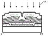
接着,在绝缘膜116上形成保护膜117。以覆盖绝缘膜114、116所具有的不平表面的方式形成保护膜117(参照图11A)。Next, a
在本实施方式中,作为保护膜117,通过溅射法形成厚度为5nm的In-Ga-Zn氧化物膜(In:Ga:Zn=1:3:2[原子%])。另外,当通过溅射法形成保护膜117时,优选的是,作为沉积气体使用氧且增高沉积气体中的氧的比例。例如,当形成In-Ga-Zn氧化物膜(In:Ga:Zn=1:3:2[原子%])时,也可以作为沉积气体使用氧且在氧为100%的气氛下进行溅射。通过增高沉积气体中的氧的比例,使保护膜117包含过剩的氧。在保护膜117包含过剩的氧的情况下,在后面添加氧时可以有效地使氧透过保护膜117。因此,可以有效地对绝缘膜114、116添加氧。In the present embodiment, as the
接着,经过保护膜117对绝缘膜114、116及氧化物半导体膜108添加氧141(参照图11B)。Next,
作为经过保护膜117对绝缘膜114、116以及氧化物半导体膜108添加氧141的方法,有离子掺杂法、离子注入法、等离子体处理法等。另外,当添加氧141时,通过对衬底一侧施加偏压可以有效地对绝缘膜114、116以及氧化物半导体膜108添加氧141。作为该偏压,例如将功率密度设定为1W/cm2以上且5W/cm2以下即可。通过在绝缘膜116上设置保护膜117然后添加氧,保护膜117被用作抑制氧从绝缘膜116脱离的保护膜。由此,可以对绝缘膜114、116以及氧化物半导体膜108添加更多量的氧。As a method of adding
另外,当利用等离子体处理引入氧时,通过利用微波使氧激发而产生高密度的氧等离子体,可以增加对绝缘膜114、116引入的氧的量。In addition, when oxygen is introduced by plasma treatment, the amount of oxygen introduced to the insulating
图12A和12B示出添加氧141时的与图11B所示的截面图不同的截面图。12A and 12B show cross-sectional views different from the cross-sectional view shown in FIG. 11B when
图12A和12B都示出通过与晶体管100相同的制造工序形成的半导体装置的一部分。图12A和12B表示的半导体装置都包括:衬底102上的绝缘膜106;绝缘膜106上的绝缘膜107;绝缘膜107上的导电膜112c;绝缘膜107及导电膜112c上的绝缘膜114;绝缘膜114上的绝缘膜116;以及绝缘膜116上的保护膜117。Both FIGS. 12A and 12B illustrate a part of a semiconductor device formed through the same manufacturing process as the
图12A示出以覆盖绝缘膜114、116的不平表面的方式形成保护膜117的情况的例子。图12B示出保护膜117不覆盖形成于绝缘膜114、116的不平表面的情况的例子。FIG. 12A shows an example of the case where the
更具体地说,在图12A中,因为保护膜117沿着由于导电膜112c形成的绝缘膜114、116的不平表面而形成,所以在添加氧141时能够抑制氧从绝缘膜114、116脱离。另一方面,在图12B中,因为保护膜117不沿着由于导电膜112c形成的绝缘膜114、116的不平的表面而形成,所以氧从图12B所示的区域144脱离。More specifically, in FIG. 12A , since the
另外,作为图12B所示的结构,有由于保护膜117的覆盖性不好而形成区域144的情况、或者在添加氧141时由于保护膜117及绝缘膜116的端部的一部分被削掉而形成区域144的情况。例如,在使用导电性高的金属膜(银、铜、铝、钛、钽、钼等的膜)形成保护膜117的情况下,在添加氧141时由于施加到衬底102一侧的偏压而在保护膜117的端部中发生电场集中,有时绝缘膜114、116及保护膜117的一部分被去除。因此,如本发明的一个方式那样,通过使用包含与氧化物半导体膜108相同的金属元素中的至少一个形成的保护膜117,能够缓和上述电场集中。In addition, as the structure shown in FIG. 12B , the
因此,如图12A所示那样,保护膜117优选以覆盖绝缘膜114、116的不平表面的方式形成。Therefore, as shown in FIG. 12A , the
接着,在保护膜117上形成绝缘膜118(参照图11C)。Next, an insulating
另外,通过在形成绝缘膜118之前或者在形成绝缘膜118之后进行加热处理,也可以使包含于绝缘膜114、116中的过剩氧释放并扩散到氧化物半导体膜108中,来填补氧化物半导体膜108中的氧空位。或者,通过进行加热形成绝缘膜118,也可以使包含于绝缘膜114、116中的过剩氧释放并扩散到氧化物半导体膜108中,来填补氧化物半导体膜108中的氧空位。此时,保护膜117抑制包含于绝缘膜114、116中的氧的外部释放和扩散。In addition, by performing heat treatment before or after the insulating
在通过PECVD法形成绝缘膜118的情况下,通过将衬底温度优选设定为300℃以上且400℃以下,更优选设定为320℃以上且370℃以下,可以形成致密的膜。When the insulating
例如,当作为绝缘膜118利用PECVD法形成氮化硅膜时,作为源气体优选使用包含硅的沉积气体、氮及氨。通过使用与氮相比少量的氨,在等离子体中氨离解而产生活性物质。该活性物质切断包含在包含硅的沉积气体中的硅与氢的键合及氮分子之间的三键。其结果是,可以形成促进硅与氮的键合且硅与氢的键合较少、缺陷较少且致密的氮化硅膜。另一方面,在相对于氮的氨量多时,包含硅的沉积气体及氮的分解未受到促进,以使形成硅与氢的键合残留且缺陷较多的不致密的氮化硅膜。由此,在源气体中,将相对于氨的氮的流量比设定为5以上且50以下,优选设定为10以上且50以下。For example, when a silicon nitride film is formed by PECVD as the insulating
在本实施方式中,作为绝缘膜118,通过利用PECVD装置并使用硅烷、氮及氨的源气体,形成厚度为50nm的氮化硅膜。硅烷的流量为50sccm,氮的流量为5000sccm,氨的流量为100sccm。将处理室的压力设定为100Pa,将衬底温度设定为350℃,用27.12MHz的高频电源对平行平板电极供应1000W的高频功率。PECVD装置是电极面积为6000cm2的平行平板型PECVD装置,将所供应的电功率的换算为每单位面积的功率(功率密度)为1.7×10⁻¹W/cm2。In the present embodiment, as the insulating
另外,在形成绝缘膜118之后也可以进行加热处理。将该加热处理的温度典型地设定为150℃以上且400℃以下,优选为300℃以上且400℃以下,更优选为320℃以上且370℃以下。由于在进行上述加热处理时绝缘膜114、116中的氢及水被减少,所以上述氧化物半导体膜108中的缺陷的产生得到抑制。In addition, heat treatment may be performed after the insulating
通过上述工序,可以制造图1A至1C所示的半导体装置。Through the above-described steps, the semiconductor device shown in FIGS. 1A to 1C can be manufactured.
<半导体装置的制造方法2><
下面,参照图13A至13D及图14A和14B对作为本发明的一个方式的半导体装置的图2A至2C所示的晶体管150的制造方法进行详细的说明。图13A至13D及图14A和14B是说明半导体装置的制造方法的截面图。13A to 13D and FIGS. 14A and 14B, a method for manufacturing the
首先,进行到图10B所示的工序为止的工序,然后在氧化物半导体膜108上形成绝缘膜114、116。(参照图13A)。First, the steps up to the step shown in FIG. 10B are performed, and then the insulating
接着,通过光刻工序在绝缘膜116上形成掩模,在绝缘膜114、116的所希望的区域中形成开口部141a、141b。开口部141a、141b到达氧化物半导体膜108(参照图13B)。Next, a mask is formed on the insulating
接着,以覆盖开口部141a、141b的方式在氧化物半导体膜108及绝缘膜116上沉积导电膜,在该导电膜上通过光刻工序形成掩模,且将该导电膜加工为所希望的区域,来形成导电膜112a及112b(参照图13C)。Next, a conductive film is deposited on the
接着,在绝缘膜116、导电膜112a及112b上形成保护膜117(参照图13D)。Next, a
接着,经过保护膜117对绝缘膜114、116及氧化物半导体膜108添加氧141(参照图14A)。Next,
另外,在图14A所示的工序中,将导电膜112a、112b用作掩模,对氧化物半导体膜108的沟道区域添加氧141。In addition, in the process shown in FIG. 14A ,
接着,在保护膜117上形成绝缘膜118(参照图14B)。Next, an insulating
通过上述工序,可以制造图2A至2C所示的半导体装置。Through the above-described processes, the semiconductor device shown in FIGS. 2A to 2C can be manufactured.
另外,关于图3A和3B所示的晶体管150A可以通过如下步骤制造:在形成绝缘膜116之后形成保护膜117;经过保护膜117添加氧;在保护膜117及绝缘膜114、116中形成到达氧化物半导体膜108的开口部141a、141b;以及以覆盖开口部141a、141b的方式形成导电膜112a、112b;在导电膜112a、112b及保护膜117上形成绝缘膜118。In addition, the
另外,关于图4A至4C所示的晶体管160,在进行图13B所示的开口部141a、141b的形成工序时,通过将绝缘膜114、116在氧化物半导体膜108上形成为岛状来制造。另外,关于图5A和5B所示的晶体管160A,在进行图13B所示的开口部141a、141b的形成工序时,通过将绝缘膜114、116及保护膜117在氧化物半导体膜108上形成为岛状来制造。In addition, the
<半导体装置的制造方法3><
下面,参照图15A至15D及图16A至16D对作为本发明的一个方式的半导体装置的晶体管170的制造方法进行详细的说明。图15A至15D及图16A至16D是说明半导体装置的制造方法的截面图。Next, a method of manufacturing the
图15A和15C及图16A和16C分别示出晶体管170的沟道长度方向的截面图,图15B和15D及图16B和16D分别示出晶体管170的沟道宽度方向的截面图。15A and 15C and FIGS. 16A and 16C respectively show cross-sectional views in the channel length direction of the
首先,进行到图11C所示的工序的工序(参照图15A和15B)。First, the process proceeds to the process shown in FIG. 11C (refer to FIGS. 15A and 15B ).
接着,通过光刻工序在绝缘膜118上形成掩模,在绝缘膜114、116、118以及保护膜117的所希望的区域中形成开口部142c。此外,通过光刻工序在绝缘膜118上形成掩模,在绝缘膜106、107、114、116、118以及保护膜117的所希望的区域中形成开口部142a、142b。开口部142c以到达导电膜112b的方式形成。此外,开口部142a、142b以都到达导电膜104的方式形成(参照图15C和15D)。Next, a mask is formed on the insulating
另外,开口部142a、142b及开口部142c既可以同时形成又可以以不同工序形成。当同时形成开口部142a、142b及开口部142c时,例如可以使用灰色调掩模或半色调掩模形成。另外,也可以在两个步骤中形成开口部142a、142b。例如,也可以加工绝缘膜106、107,然后加工绝缘膜114、116、118及保护膜117。In addition, the
接着,以覆盖开口部142a、142b、142c的方式在绝缘膜118上形成导电膜120(参照图16A和16B)。Next, the
作为导电膜120,例如可以使用包含选自铟(In)、锌(Zn)和锡(Sn)中的一种的材料。导电膜120尤其可以使用包含氧化钨的铟氧化物、包含氧化钨的铟锌氧化物、包含氧化钛的铟氧化物、包含氧化钛的铟锡氧化物、铟锡氧化物(ITO)、铟锌氧化物、添加有氧化硅的铟锡氧化物(Indium Tin SiO2doped Oxide:以下称为ITSO)等透光导电材料。此外,例如可以使用溅射法形成导电膜120。在本实施方式中,通过溅射法形成膜厚度为110nm的ITSO膜。As the
接着,通过光刻工序在导电膜120上形成掩模,将导电膜120加工为所希望的区域,来形成导电膜120a、120b(参照图16C和16D)。Next, a mask is formed on the
通过上述步骤,可以制造图6A至6C所示的晶体管170。Through the above steps, the
另外,关于图7A和7B所示的晶体管170A,在进行图16C和16D所示的工序之后,通过在导电膜120a、120b及绝缘膜118上形成绝缘膜122来制造。In addition, the
〈半导体装置的制造方法4〉<
下面,参照图17A至17F、图18A至18F及图19A至19F对作为本发明的一个方式的半导体装置的图7C和7D所示的晶体管170B的制造方法进行详细的说明。图17A至17F、图18A至18F及图19A至19F是说明半导体装置的制造方法的截面图。17A to 17F , FIGS. 18A to 18F , and FIGS. 19A to 19F , a method for manufacturing the
图17A、17C和17E、图18A、18C和18E、以及图19A、19C和19E分别示出晶体管170B的沟道长度方向的截面图,图17B、17D和17F、图18B、18D和18F、以及图19B、19D和19F分别示出晶体管170B的沟道宽度方向的截面图。17A, 17C, and 17E, FIGS. 18A, 18C, and 18E, and FIGS. 19A, 19C, and 19E, respectively, show cross-sectional views in the channel length direction of
首先,进行到图10B所示的工序的工序,然后在氧化物半导体膜108及绝缘膜107上形成导电膜112及绝缘膜116。(参照图17A和17B)。First, the process proceeds to the process shown in FIG. 10B , and then the
可以使用可用于导电膜112a、112b的任何材料及任何方法形成导电膜112。The
接着,在绝缘膜116上的所希望的区域中形成掩模140a、140b(参照图17C和17D)。Next,
接着,从掩模140a、140b上使用蚀刻气体142,对绝缘膜116及导电膜112进行加工(参照图17E和17F)。Next, the insulating
另外,在使用湿蚀刻装置对绝缘膜116及导电膜112进行加工的情况下,也可以使用化学溶液代替蚀刻气体142。另外,也可以使用湿蚀刻装置和干蚀刻装置的双方对绝缘膜116及导电膜112进行加工。In addition, when the insulating
接着,通过去除掩模140a、140b,形成导电膜112a、112b及绝缘膜116a、116b。然后,在氧化物半导体膜108、导电膜112a、112b及绝缘膜116a、116b上形成绝缘膜114(参照图18A和18B)。Next, by removing the
另外,也可以在形成绝缘膜114之前对氧化物半导体膜108的表面(背沟道一侧)进行清洁。作为该清洁方法,例如可以举出使用磷酸等化学溶液的清洁。通过进行使用磷酸等化学溶液的清洁,可以去除附着在氧化物半导体膜108的表面上的杂质(例如,包含在导电膜112a、112b及绝缘膜116a、116b中的元素等)。In addition, the surface (back channel side) of the
在形成导电膜112a、112b及绝缘膜116a、116b的工序及/或在上述清洁工序中,有时凹部形成在氧化物半导体膜108的一部分中。In the step of forming the
接着,在绝缘膜114上形成保护膜117,将氧141经过保护膜117添加到绝缘膜114、116(参照图18C和18D)。Next, a
接着,在保护膜117上形成绝缘膜118(参照图18E和18F)。Next, an insulating
接着,通过光刻工序在绝缘膜118上形成掩模,在绝缘膜114、116、118以及保护膜117的所希望的区域中形成开口部142c。此外,通过光刻工序在绝缘膜118上形成掩模,在绝缘膜106、107、114、116、118以及保护膜117的所希望的区域中形成开口部142a、142b。开口部142c到达导电膜112b。此外,开口部142a、142b到达导电膜104(参照图19A和19B)。Next, a mask is formed on the insulating
接着,以覆盖开口部142a、142b、142c的方式在绝缘膜118上形成导电膜120(参照图19C和19D)。Next, the
接着,通过光刻工序在导电膜120上形成掩模,将导电膜120加工为所希望的区域,来形成导电膜120a、120b(参照图19E和19F)。Next, a mask is formed on the
通过上述步骤,可以制造图7C和7D所示的晶体管170B。Through the above steps, the
在本实施方式中,描述了本发明的一个方式。其他实施方式描述在实施方式2至4中。本发明的一个方式不局限于此。虽然作为本发明的一个方式示出晶体管100等包含氧化物半导体膜的例子,但是本发明的一个方式不局限于此。根据情形或状况,本发明的一个方式晶体管100等也可以不包含氧化物半导体膜。例如,在本发明的一个方式中,根据情况或状况,也可以使用包含Si(硅)、Ge(锗)、SiGe(硅锗)、GaAs(砷化镓)等的材料形成晶体管100等的沟道及沟道、源区域及漏区域等的附近。In this embodiment, one form of the present invention is described. Other embodiments are described in
本实施方式所示的结构、方法可以与其他实施方式所示的结构、方法适当地组合而使用。The structures and methods shown in this embodiment can be used in combination with the structures and methods shown in other embodiments as appropriate.
实施方式2
在本实施方式中,以下详细说明本发明的一个方式的半导体装置所具有的氧化物半导体。In this embodiment mode, the oxide semiconductor included in the semiconductor device according to one embodiment of the present invention will be described in detail below.
<氧化物半导体的结构><Structure of oxide semiconductor>
首先,对氧化物半导体的结构进行说明。First, the structure of the oxide semiconductor will be described.
氧化物半导体被分为单晶氧化物半导体和非单晶氧化物半导体。作为非单晶氧化物半导体有CAAC-OS(C-Axis Aligned Crystalline Oxide Semiconductor:c轴取向结晶氧化物半导体)、多晶氧化物半导体、nc-OS(nanocrystalline Oxide Semiconductor:纳米晶氧化物半导体)、类a的OS(amorphous like Oxide Semiconductor,类非晶的氧化物半导体)以及非晶氧化物半导体等。Oxide semiconductors are classified into single crystal oxide semiconductors and non-single crystal oxide semiconductors. Examples of non-single crystal oxide semiconductors include CAAC-OS (C-Axis Aligned Crystalline Oxide Semiconductor: c-axis oriented crystalline oxide semiconductor), polycrystalline oxide semiconductor, nc-OS (nanocrystalline Oxide Semiconductor: nanocrystalline oxide semiconductor), A-like OS (amorphous like Oxide Semiconductor, amorphous oxide semiconductor) and amorphous oxide semiconductor, etc.
从其他观点看来,氧化物半导体被分为非晶氧化物半导体和结晶氧化物半导体。作为结晶氧化物半导体的例子包括单晶氧化物半导体、CAAC-OS、多晶氧化物半导体以及nc-OS。From other viewpoints, oxide semiconductors are classified into amorphous oxide semiconductors and crystalline oxide semiconductors. Examples of the crystalline oxide semiconductor include single crystal oxide semiconductor, CAAC-OS, polycrystalline oxide semiconductor, and nc-OS.
作为非晶结构的定义,一般而言,已知:它成为介稳状态并没有固定化,它为各向同性且不具有不均匀结构。换句话说,非晶结构具有灵活键角并具有短程有序性而不具有长程有序性。As a definition of an amorphous structure, generally speaking, it is known that it becomes a metastable state and is not immobilized, and that it is isotropic and does not have an inhomogeneous structure. In other words, the amorphous structure has flexible bond angles and has short-range order but not long-range order.
这意味着不能将实质上稳定的氧化物半导体称为完全非晶(completelyamorphous)氧化物半导体。另外,不能将不具有各向同性(例如,在微观区域中具有周期结构)的氧化物半导体称为完全非晶氧化物半导体。注意,类a的OS在微观区域中具有周期结构,但是同时具有空位(也称为void),并具有不稳定结构。因此,类a的OS具有近乎于非晶氧化物半导体的物性。This means that a substantially stable oxide semiconductor cannot be called a completely amorphous oxide semiconductor. In addition, an oxide semiconductor that does not have isotropy (eg, has a periodic structure in a microscopic region) cannot be called a completely amorphous oxide semiconductor. Note that the OS of class a has a periodic structure in the microscopic region, but at the same time has vacancies (also called voids), and has an unstable structure. Therefore, the a-like OS has physical properties close to those of an amorphous oxide semiconductor.
<CAAC-OS><CAAC-OS>
首先,对CAAC-OS进行说明。First, CAAC-OS will be described.
CAAC-OS是包含多个c轴取向的结晶部(也称为颗粒)的氧化物半导体之一。CAAC-OS is one of oxide semiconductors including a plurality of c-axis-oriented crystal parts (also referred to as particles).
在利用透射电子显微镜(TEM:Transmission Electron Microscope)观察所得到的CAAC-OS的明视场图像与衍射图案的复合分析图像(也称为高分辨率TEM图像)中,观察到多个颗粒。然而,在高分辨率TEM图像中,观察不到颗粒与颗粒之间的明确的边界,即晶界(grain boundary)。因此,可以说在CAAC-OS中,不容易发生起因于晶界的电子迁移率的降低。In a composite analysis image (also referred to as a high-resolution TEM image) of the bright-field image of CAAC-OS and the diffraction pattern obtained by observation with a transmission electron microscope (TEM: Transmission Electron Microscope), many particles were observed. However, in high-resolution TEM images, clear boundaries between particles, ie, grain boundaries, are not observed. Therefore, it can be said that in CAAC-OS, the decrease in electron mobility due to grain boundaries does not easily occur.
下面,对利用TEM观察的CAAC-OS进行说明。图37A示出从大致平行于样品面的方向观察所得到的CAAC-OS的截面的高分辨率TEM图像。利用球面像差校正(SphericalAberration Corrector)功能得到高分辨率TEM图像。将利用球面像差校正功能所得到的高分辨率TEM图像特别称为Cs校正高分辨率TEM图像。例如可以使用日本电子株式会社(JEOLltd)制造的原子分辨率分析型电子显微镜JEM-ARM200F等得到Cs校正高分辨率TEM图像。Next, CAAC-OS observed by TEM will be described. FIG. 37A shows a high-resolution TEM image of a cross-section of the resulting CAAC-OS viewed from a direction approximately parallel to the sample surface. High-resolution TEM images were obtained using the Spherical Aberration Corrector function. The high-resolution TEM image obtained by utilizing the spherical aberration correction function is particularly referred to as a Cs-corrected high-resolution TEM image. For example, a Cs-corrected high-resolution TEM image can be obtained using an atomic resolution analytical electron microscope JEM-ARM200F manufactured by JEOL Ltd., or the like.
图37B示出将图37A中的区域(1)放大的Cs校正高分辨率TEM图像。由图37B可以确认到在颗粒中金属原子排列为层状。各金属原子层具有反映了形成CAAC-OS膜的面(下面,该面被称为形成面)或CAAC-OS的顶面的不平度的配置并以平行于CAAC-OS的形成面或顶面的方式排列。Fig. 37B shows a Cs-corrected high-resolution TEM image magnified of region (1) in Fig. 37A. From FIG. 37B , it was confirmed that the metal atoms were arranged in layers in the particles. Each metal atomic layer has a configuration reflecting the unevenness of the surface on which the CAAC-OS film is formed (hereinafter, this surface is referred to as the formation surface) or the top surface of the CAAC-OS and is arranged in parallel with the formation surface or the top surface of the CAAC-OS. arranged in a manner.
如图37B所示,CAAC-OS具有特有的原子排列。图37C是以辅助线示出特有的原子排列的图。由图37B和图37C可知,一个颗粒的尺寸为1nm以上且3nm以下左右,由颗粒与颗粒之间的倾斜产生的空隙的尺寸为0.8nm左右。因此,也可以将颗粒称为纳米晶(nc:nanocrystal)。注意,也可以将CAAC-OS称为具有CANC(C-Axis Aligned nanocrystals:c轴取向纳米晶)的氧化物半导体。As shown in Figure 37B, CAAC-OS has a characteristic atomic arrangement. FIG. 37C is a diagram showing a characteristic atomic arrangement with an auxiliary line. As can be seen from FIGS. 37B and 37C , the size of one particle is about 1 nm or more and 3 nm or less, and the size of the voids generated by the inclination between the particles is about 0.8 nm. Therefore, the particles may also be referred to as nanocrystals (nc: nanocrystals). Note that CAAC-OS may also be referred to as an oxide semiconductor with CANC (C-Axis Aligned nanocrystals).
在此,根据Cs校正高分辨率TEM图像,将衬底5120上的CAAC-OS的颗粒5100的配置示意性地表示为堆积砖块或块体的结构(参照图37D)。在图37C中观察到的颗粒产生倾斜的部分相当于图37D所示的区域5161。Here, the configuration of the particles 5100 of CAAC-OS on the substrate 5120 is schematically represented as a structure of stacked bricks or blocks based on the Cs-corrected high-resolution TEM image (refer to FIG. 37D ). The portion where the particle is inclined observed in Fig. 37C corresponds to the region 5161 shown in Fig. 37D.
图38A示出从大致垂直于样品面的方向观察所得到的CAAC-OS的平面的Cs校正高分辨率TEM图像。图38B、图38C和图38D分别示出将图38A中的区域(1)、区域(2)和区域(3)放大的Cs校正高分辨率TEM图像。由图38B、图38C和图38D可知在颗粒中金属原子排列为三角形状、四角形状或六角形状。但是,在不同的颗粒之间金属原子的排列没有规律性。FIG. 38A shows a Cs-corrected high-resolution TEM image of the plane of the resulting CAAC-OS viewed from a direction approximately perpendicular to the sample surface. Figures 38B, 38C, and 38D show enlarged Cs-corrected high-resolution TEM images of Region (1), Region (2), and Region (3) in Figure 38A, respectively. It can be seen from FIGS. 38B , 38C and 38D that the metal atoms are arranged in a triangular shape, a quadrangular shape or a hexagonal shape in the particles. However, there is no regularity in the arrangement of metal atoms between different particles.
接着,说明使用X射线衍射(XRD:X-Ray Diffraction)进行分析的CAAC-OS。例如,当利用平面外(out-of-plane)法分析包含InGaZnO4结晶的CAAC-OS的结构时,如图39A所示,在衍射角(2θ)为31°附近时出现峰值。由于该峰值来源于InGaZnO4结晶的(009)面,由此可知CAAC-OS中的结晶具有c轴取向性,并且c轴朝向大致垂直于CAAC-OS的形成面或顶面的方向。Next, CAAC-OS analyzed by X-ray diffraction (XRD: X-Ray Diffraction) will be described. For example, when the structure of CAAC-OS including InGaZnO4 crystals is analyzed by the out-of-plane method, as shown in FIG. 39A , a peak appears when the diffraction angle (2θ) is around 31°. Since this peak is derived from the (009) plane of the InGaZnO4 crystal, it is understood that the crystal in CAAC-OS has c-axis orientation, and the c-axis is oriented in a direction substantially perpendicular to the formation surface or top surface of CAAC-OS.
注意,当利用平面外法分析CAAC-OS的结构时,除了2θ为31°附近的峰值以外,有时在2θ为36°附近时也出现峰值。2θ为36°附近的峰值表示CAAC-OS中的一部分包含不具有c轴取向性的结晶。优选的是,在利用平面外法分析的CAAC-OS的结构中,在2θ为31°附近时出现峰值而在2θ为36°附近时不出现峰值。Note that when the structure of CAAC-OS was analyzed by the out-of-plane method, in addition to the peak at 2θ around 31°, a peak sometimes appeared at around 36° 2θ. The peak near 36° in 2θ indicates that a part of CAAC-OS contains crystals that do not have c-axis orientation. Preferably, in the structure of CAAC-OS analyzed by the out-of-plane method, a peak appears when 2θ is around 31° and no peak appears when 2θ is around 36°.
另一方面,当利用从大致垂直于c轴的方向使X射线入射到样品的平面内(in-plane)法分析CAAC-OS的结构时,在2θ为56°附近时出现峰值。该峰值来源于InGaZnO4结晶的(110)面。在CAAC-OS中,当将2θ固定为56°附近并在以样品面的法线向量为轴(φ轴)旋转样品的条件下进行分析(φ扫描)时,如图39B所示的那样观察不到明确的峰值。相比之下,在InGaZnO4的单晶氧化物半导体中,在将2θ固定为56°附近来进行φ扫描时,如图39C所示的那样观察到来源于相等于(110)面的结晶面的六个峰值。因此,由使用XRD的结构分析可以确认在CAAC-OS中的a轴和b轴的取向没有规律性。On the other hand, when the structure of CAAC-OS is analyzed by the in-plane method in which X-rays are incident on the sample from a direction substantially perpendicular to the c-axis, a peak appears when 2θ is around 56°. This peak originates from the (110) plane of the InGaZnO4 crystal. In CAAC-OS, when 2θ is fixed at around 56° and the sample is rotated with the normal vector of the sample surface as the axis (φ axis), the analysis (φ scan) is performed, as shown in FIG. 39B . less than a clear peak. In contrast, in the single crystal oxide semiconductor of InGaZnO4 , when φ scan is performed with 2θ fixed at around 56°, a crystal plane derived from the (110) plane is observed as shown in FIG. 39C . of six peaks. Therefore, it can be confirmed from the structural analysis using XRD that there is no regularity in the orientation of the a-axis and the b-axis in the CAAC-OS.
接着,说明利用电子衍射进行分析的CAAC-OS。例如,当对包含InGaZnO4结晶的CAAC-OS在平行于样品面的方向上入射束径为300nm的电子束时,可能会获得图40A所示的衍射图案(也称为选区透射电子衍射图案)。在该衍射图案中包含起因于InGaZnO4结晶的(009)面的斑点。因此,由电子衍射也可知CAAC-OS所包含的颗粒具有c轴取向性,并且c轴朝向大致垂直于CAAC-OS的形成面或顶面的方向。另一方面,图40B示出对相同的样品在垂直于样品面的方向上入射束径为300nm的电子束时的衍射图案。由图40B观察到环状的衍射图案。因此,由电子衍射也可知CAAC-OS所包含的颗粒的a轴和b轴不具有取向性。可以认为图40B中的第一环起因于InGaZnO4结晶的(010)面和(100)面等。另外,可以认为图40B中的第二环起因于(110)面等。Next, CAAC-OS analyzed by electron diffraction will be described. For example, when an electron beam with a beam diameter of 300 nm is incident on a CAAC- OS containing InGaZnO crystals in a direction parallel to the sample surface, a diffraction pattern as shown in Fig. 40A (also called a selected area transmission electron diffraction pattern) may be obtained. . The diffraction pattern includes spots originating from the (009) plane of the InGaZnO4 crystal. Therefore, it can be seen from electron diffraction that the particles contained in the CAAC-OS have c-axis orientation, and the c-axis is oriented in a direction substantially perpendicular to the formation surface or the top surface of the CAAC-OS. On the other hand, FIG. 40B shows the diffraction pattern when an electron beam having a beam diameter of 300 nm is incident on the same sample in a direction perpendicular to the sample surface. A ring-shaped diffraction pattern is observed from FIG. 40B . Therefore, the a-axis and b-axis of the particle|grains contained in CAAC-OS have no orientation property also from electron diffraction. It is considered that the first ring in FIG. 40B originates from the (010) plane, the (100) plane, and the like of the InGaZnO4 crystal. In addition, the second loop in FIG. 40B can be considered to be caused by the (110) plane or the like.
如上所述,CAAC-OS是结晶性高的氧化物半导体。氧化物半导体的结晶性有时因杂质的混入或缺陷的生成等而降低。这意味着CAAC-OS是杂质或缺陷(氧空位等)少的氧化物半导体。As described above, CAAC-OS is an oxide semiconductor with high crystallinity. The crystallinity of an oxide semiconductor may be lowered due to contamination of impurities, generation of defects, or the like. This means that CAAC-OS is an oxide semiconductor with few impurities or defects (oxygen vacancies, etc.).
另外,杂质是指氧化物半导体的主要成分以外的元素,诸如氢、碳、硅和过渡金属元素等。例如,与氧的键合力比包含在氧化物半导体中的金属元素强的元素(具体而言,硅等)会夺取从氧化物半导体的氧,由此导致氧化物半导体的原子排列的杂乱以及结晶性下降。另外,由于铁或镍等的重金属、氩、二氧化碳等的原子半径(或分子半径)大,所以会打乱氧化物半导体的原子排列,导致结晶性下降。In addition, the impurities refer to elements other than the main components of the oxide semiconductor, such as hydrogen, carbon, silicon, transition metal elements, and the like. For example, an element (specifically, silicon, etc.) having a stronger bonding force with oxygen than a metal element contained in the oxide semiconductor robs oxygen from the oxide semiconductor, thereby causing disorder in the atomic arrangement of the oxide semiconductor and crystallization Sexual decline. In addition, since heavy metals such as iron and nickel, argon, carbon dioxide, and the like have large atomic radii (or molecular radii), the atomic arrangement of the oxide semiconductor is disturbed, resulting in a decrease in crystallinity.
具有杂质或缺陷的氧化物半导体的特性有时因光或热等会发生变动。例如,包含于氧化物半导体中的杂质有时会成为载流子陷阱或载流子发生源。另外,氧化物半导体中的氧空位会成为载流子陷阱或在俘获氢时成为载流子发生源。The properties of an oxide semiconductor having impurities or defects may vary due to light, heat, or the like. For example, impurities contained in an oxide semiconductor may become a carrier trap or a carrier generation source. In addition, oxygen vacancies in the oxide semiconductor serve as a carrier trap or a carrier generation source when hydrogen is trapped.
杂质及氧空位少的CAAC-OS是载流子密度低的氧化物半导体。具体而言,可以使载流子密度小于8×10¹¹/cm3,优选小于1×1011/cm3,更优选小于1×1010/cm3,且是1×10-9/cm3以上。将这样的氧化物半导体称为高纯度本征或实质上高纯度本征的氧化物半导体。CAAC-OS的杂质浓度和缺陷态密度低。因此,CAAC-OS可以被称为具有稳定特性的氧化物半导体。CAAC-OS with few impurities and oxygen vacancies is an oxide semiconductor with low carrier density. Specifically, the carrier density can be made smaller than 8×10¹¹ /cm3 , preferably smaller than 1×10¹¹ /cm3 , more preferably smaller than 1×10¹⁰ /cm3 , and 1×10⁻⁹ /cm3 above. Such an oxide semiconductor is called a high-purity intrinsic or substantially high-purity intrinsic oxide semiconductor. The impurity concentration and defect state density of CAAC-OS are low. Therefore, CAAC-OS can be called an oxide semiconductor with stable characteristics.
<nc-OS><nc-OS>
接着说明nc-OS。Next, nc-OS will be described.
nc-OS在高分辨率TEM图像中具有观察到结晶部的区域和观察不到明确的结晶部的区域。nc-OS所包含的结晶部的尺寸大多为1nm以上且10nm以下或1nm以上且3nm以下。注意,有时将其结晶部的尺寸大于10nm且是100nm以下的氧化物半导体称为微晶氧化物半导体。例如,在nc-OS的高分辨率TEM图像中,有时无法明确地观察到晶界。注意,纳米晶的来源有可能与CAAC-OS中的颗粒相同。因此,下面有时将nc-OS的结晶部称为颗粒。In the high-resolution TEM image, nc-OS has a region where crystal parts are observed and a region where no clear crystal parts are observed. The size of the crystal part included in nc-OS is often 1 nm or more and 10 nm or less, or 1 nm or more and 3 nm or less. Note that an oxide semiconductor whose crystal portion size is larger than 10 nm and 100 nm or less may be referred to as a microcrystalline oxide semiconductor. For example, in high-resolution TEM images of nc-OS, grain boundaries are sometimes not clearly observed. Note that it is possible that the source of nanocrystals is the same as the particles in CAAC-OS. Therefore, the crystal part of nc-OS is sometimes referred to as a particle below.
在nc-OS中,微观的区域(例如1nm以上且10nm以下的区域,特别是1nm以上且3nm以下的区域)中的原子排列具有周期性。另外,nc-OS在不同的颗粒之间没有结晶取向的规律性。因此,观察不到膜整体的取向性。所以,nc-OS不能够根据分析方法与类a的OS和非晶氧化物半导体区别开来。例如,当利用使用其束径比颗粒大的X射线的平面外法对nc-OS进行结构分析时,检测不到表示结晶面的峰值。在使用其束径比颗粒的尺寸大(例如,50nm以上)的电子射线对nc-OS进行电子衍射时,观察到类似光晕图案的衍射图案。另一方面,在使用其束径近于颗粒的尺寸或者比颗粒的尺寸小的电子射线时,nc-OS在纳米束电子衍射图案呈现斑点。另外,在nc-OS的纳米束电子衍射图案中,有时观察到如圆圈那样的(环状的)亮度高的区域。而且,在nc-OS的纳米束电子衍射图案中,有时还观察到环状的区域内的多个斑点。In nc-OS, the atomic arrangement in a microscopic region (for example, a region of 1 nm or more and 10 nm or less, in particular, a region of 1 nm or more and 3 nm or less) has periodicity. In addition, nc-OS has no regularity of crystallographic orientation among different particles. Therefore, the orientation of the whole film was not observed. Therefore, nc-OS cannot be distinguished from a-like OS and amorphous oxide semiconductor according to the analytical method. For example, when the structure of nc-OS is analyzed by the out-of-plane method using X-rays whose beam diameter is larger than that of particles, no peaks representing crystal planes are detected. When the nc-OS is electron-diffracted using electron rays whose beam diameter is larger than the particle size (eg, 50 nm or more), a halo pattern-like diffraction pattern is observed. On the other hand, when an electron beam whose beam diameter is close to or smaller than the particle size is used, nc-OS exhibits speckle in the nanobeam electron diffraction pattern. In addition, in the nanobeam electron diffraction pattern of nc-OS, a region with high brightness such as a circle (ring-shaped) may be observed. Furthermore, in the nanobeam electron diffraction pattern of nc-OS, a plurality of spots in a ring-shaped region may be observed.
如此,由于在颗粒(纳米晶)之间结晶取向都没有规律性,所以也可以将nc-OS称为包含RANC(Random Aligned nanocrystals:无规取向纳米晶)的氧化物半导体或包含NANC(Non-Aligned nanocrystals:无取向纳米晶)的氧化物半导体。In this way, since there is no regularity in crystal orientation among particles (nanocrystals), nc-OS can also be called an oxide semiconductor containing RANC (Random Aligned nanocrystals) or an oxide semiconductor containing NANC (Non- Aligned nanocrystals: Non-oriented nanocrystals) oxide semiconductors.
nc-OS是规律性比非晶氧化物半导体高的氧化物半导体。因此,nc-OS的缺陷态密度比类a的OS或非晶氧化物半导体低。但是,在nc-OS中的不同的颗粒之间没有晶体取向的规律性。所以,nc-OS的缺陷态密度比CAAC-OS高。nc-OS is an oxide semiconductor with higher regularity than an amorphous oxide semiconductor. Therefore, the density of defect states of nc-OS is lower than that of a-like OS or amorphous oxide semiconductors. However, there is no regularity of crystal orientation among different particles in nc-OS. Therefore, the defect state density of nc-OS is higher than that of CAAC-OS.
<类a的OS><OS of class a>
类a的OS具有介于nc-OS与非晶氧化物半导体之间的结构。The OS of class a has a structure intermediate between nc-OS and amorphous oxide semiconductor.
在类a的OS的高分辨率TEM图像中有时观察到空位。另外,在高分辨率TEM图像中,有明确地观察到结晶部的区域和不观察到结晶部的区域。Vacancies are sometimes observed in high-resolution TEM images of a-like OS. In addition, in the high-resolution TEM image, there are regions where crystal parts are clearly observed and regions where crystal parts are not observed.
由于类a的OS包含空洞,所以其结构不稳定。为了证明与CAAC-OS及nc-OS相比类a的OS具有不稳定的结构,下面示出电子照射所导致的结构变化。Since the OS of class a contains holes, its structure is unstable. In order to prove that the a-like OS has an unstable structure compared with CAAC-OS and nc-OS, the structural change by electron irradiation is shown below.
作为进行电子照射的样品,准备类a的OS(样品A)、nc-OS(样品B)和CAAC-OS(样品C)。每个样品都是In-Ga-Zn氧化物。As samples for electron irradiation, OS of class a (sample A), nc-OS (sample B), and CAAC-OS (sample C) were prepared. Each sample is In-Ga-Zn oxide.
首先,取得各样品的高分辨率截面TEM图像。由高分辨率截面TEM图像可知,所有样品都具有结晶部。First, a high-resolution cross-sectional TEM image of each sample is acquired. From the high-resolution cross-sectional TEM images, it was found that all the samples had crystal parts.
注意,如下那样决定将哪个部分作为一个结晶部。已知InGaZnO4结晶的晶胞具有包括三个In-O层和六个Ga-Zn-O层的九个层在c轴方向上层叠的结构。这些彼此靠近的层之间的间隔与(009)面的晶格表面间隔(也称为d值)是相等的。由结晶结构分析求出其值为0.29nm。由此,可以将晶格条纹的间隔为0.28nm以上且0.30nm以下的部分作为InGaZnO4结晶部。每个晶格条纹对应于InGaZnO4结晶的a-b面。Note that which part is determined as one crystal part is determined as follows. It is known that the unit cell of the InGaZnO4 crystal has a structure in which nine layers including three In-O layers and six Ga-Zn-O layers are stacked in the c-axis direction. The spacing between these adjacent layers is equal to the lattice surface spacing of the (009) plane (also referred to as the d value). The value was found to be 0.29 nm from the crystal structure analysis. Thereby, the part where the interval of the lattice fringes is 0.28 nm or more and 0.30 nm or less can be used as the InGaZnO4 crystal part. Each lattice fringe corresponds to the ab plane of theInGaZnO crystal.
图41示出各样品的结晶部(22个点至45个点)的平均尺寸的变化。注意,结晶部尺寸对应于上述晶格条纹的长度。由图41可知,在类a的OS中,结晶部尺寸根据电子的累积照射量逐渐变大。具体而言,如图41中的(1)所示,可知在利用TEM的观察初期尺寸为1.2nm左右的结晶部(该结晶部也称为初始晶核)在累积照射量为4.2×10⁸e-/nm2时生长到2.6nm左右的尺寸。另一方面,可知nc-OS和CAAC-OS在开始电子照射时到电子的累积照射量为4.2×108e-/nm2,结晶部的尺寸几乎没有变化。具体而言,如图41中的(2)及(3)所示,无论电子的累积照射量如何,nc-OS及CAAC-OS的平均结晶部尺寸都分别为1.4nm左右及2.1nm左右。FIG. 41 shows the change in the average size of the crystal parts (22 points to 45 points) of each sample. Note that the crystal portion size corresponds to the length of the above-described lattice fringes. As can be seen from FIG. 41 , in the OS of class a, the crystal part size gradually increases according to the cumulative irradiation amount of electrons. Specifically, as shown in (1) in FIG. 41 , it was found that the crystal portion (this crystal portion is also referred to as an initial crystal nucleus) having an initial size of about 1.2 nm in the observation by TEM has a cumulative irradiation dose of 4.2×10⁸ It grows to a size of about 2.6 nm at e- /nm2 . On the other hand, it was found that the cumulative irradiation dose to electrons at the start of electron irradiation for nc-OS and CAAC-OS was 4.2×10⁸ e− /nm2 , and the size of the crystal portion hardly changed. Specifically, as shown in (2) and (3) of FIG. 41 , regardless of the cumulative irradiation amount of electrons, the average crystal part sizes of nc-OS and CAAC-OS were about 1.4 nm and about 2.1 nm, respectively.
如此,电子照射引起类a的OS中的结晶部的生长。另一方面,在nc-OS和CAAC-OS中,几乎没有电子照射所引起的结晶部的生长。也就是说,类a的OS与CAAC-OS及nc-OS相比具有不稳定的结构。In this way, the electron irradiation causes the growth of crystal parts in the a-like OS. On the other hand, in nc-OS and CAAC-OS, there is almost no growth of crystal parts by electron irradiation. That is, the OS of class a has an unstable structure compared to CAAC-OS and nc-OS.
另外,由于类a的OS包含空洞,所以其密度比nc-OS及CAAC-OS低。具体地,类a的OS的密度为具有相同组成的单晶氧化物半导体的78.6%以上且小于92.3%。nc-OS的密度及CAAC-OS的密度为具有相同组成的单晶氧化物半导体的92.3%以上且小于100%。注意,难以沉积其密度小于单晶氧化物半导体的密度的78%的氧化物半导体。In addition, since the OS of class a contains holes, its density is lower than that of nc-OS and CAAC-OS. Specifically, the density of the OS of class a is 78.6% or more and less than 92.3% of that of a single crystal oxide semiconductor having the same composition. The density of nc-OS and the density of CAAC-OS are 92.3% or more and less than 100% of the single crystal oxide semiconductors having the same composition. Note that it is difficult to deposit an oxide semiconductor whose density is less than 78% of that of a single crystal oxide semiconductor.
例如,在具有In:Ga:Zn=1:1:1的原子数比的氧化物半导体的情况下,具有菱方晶系结构的单晶InGaZnO4的密度为6.357g/cm3。因此,在具有In:Ga:Zn=1:1:1的原子数比的氧化物半导体的情况下,类a的OS的密度为5.0g/cm3以上且小于5.9g/cm3。例如,在具有In:Ga:Zn=1:1:1的原子数比的氧化物半导体的情况下,nc-OS的密度和CAAC-OS的密度为5.9g/cm3以上且小于6.3g/cm3。For example, in the case of an oxide semiconductor having an atomic ratio of In:Ga:Zn=1:1:1, the density of single crystal InGaZnO4 having a rhombohedral structure is 6.357 g/cm3 . Therefore, in the case of an oxide semiconductor having an atomic ratio of In:Ga:Zn=1:1:1, the density of the a-like OS is 5.0 g/cm3 or more and less than 5.9 g/cm3 . For example, in the case of an oxide semiconductor having an atomic ratio of In:Ga:Zn=1:1:1, the density of nc-OS and the density of CAAC-OS are 5.9 g/cm3 or more and less than 6.3 g/cm cm3 .
注意,有时具有特定组成的氧化物半导体不能够存在于单晶结构中。此时,通过以任意比例组合组成不同的单晶氧化物半导体,可以估计出具有所希望的组成的单晶氧化物半导体的密度。根据组成不同的单晶氧化物半导体的组合比例使用加权平均计算出具有所希望的组成的单晶氧化物半导体的密度即可。注意,优选尽可能减少单晶氧化物半导体的种类来计算密度。Note that sometimes an oxide semiconductor having a specific composition cannot exist in a single crystal structure. At this time, by combining the single crystal oxide semiconductors of different compositions in an arbitrary ratio, the density of the single crystal oxide semiconductor having a desired composition can be estimated. The density of the single crystal oxide semiconductor having a desired composition may be calculated using a weighted average from the combination ratio of the single crystal oxide semiconductors having different compositions. Note that it is preferable to calculate the density by reducing the types of single crystal oxide semiconductors as much as possible.
如上所述,氧化物半导体具有各种结构及各种特性。注意,氧化物半导体例如可以是包括非晶氧化物半导体、类a的OS、nc-OS和CAAC-OS中的两种以上的叠层膜。As described above, oxide semiconductors have various structures and various properties. Note that the oxide semiconductor may be, for example, a stacked film including two or more of amorphous oxide semiconductor, a-like OS, nc-OS, and CAAC-OS.
本实施方式所示的结构、方法等可以与其他实施方式所示的结构、方法等适当地组合。The structures, methods, and the like shown in this embodiment can be appropriately combined with the structures, methods, and the like shown in other embodiments.
实施方式3
在本实施方式中,使用图20、图21及图22说明包括在前面的实施方式中说明的任何晶体管的显示装置的一个例子。In this embodiment mode, an example of a display device including any of the transistors described in the previous embodiment mode will be described using FIGS. 20 , 21 , and 22 .
图20是示出显示装置的一个例子的俯视图。图20所示的显示装置700包括:设置在第一衬底701上的像素部702;设置在第一衬底701上的源极驱动电路部704及栅极驱动电路部706;以围绕像素部702、源极驱动电路部704及栅极驱动电路部706的方式设置的密封剂712;以及以与第一衬底701对置的方式设置的第二衬底705。注意,由密封剂712密封第一衬底701及第二衬底705。也就是说,像素部702、源极驱动电路部704及栅极驱动电路部706被第一衬底701、密封剂712及第二衬底705密封。注意,虽然在图20中未图示,但是在第一衬底701与第二衬底705之间设置有显示元件。FIG. 20 is a plan view showing an example of a display device. The
另外,在显示装置700中,在与位于第一衬底701上的由密封剂712围绕的区域不同的区域中,设置有与像素部702、源极驱动电路部704及栅极驱动电路部706电连接的FPC(Flexible printed circuit:柔性印刷电路)端子部708。另外,FPC 716连接于FPC端子部708,并且通过FPC 716对像素部702、源极驱动电路部704及栅极驱动电路部706供应各种信号等。另外,像素部702、源极驱动电路部704、栅极驱动电路部706以及FPC端子部708都与信号线710连接。从FPC 716供应的各种信号等是通过信号线710供应到像素部702、源极驱动电路部704、栅极驱动电路部706及FPC端子部708。In addition, in the
另外,也可以在显示装置700中设置多个栅极驱动电路部706。另外,作为显示装置700,虽然示出将源极驱动电路部704及栅极驱动电路部706形成在与像素部702相同的衬底即第一衬底701上的例子,但是不局限于该结构。例如,也可以仅将栅极驱动电路部706形成在第一衬底701上,又可以仅将源极驱动电路部704形成在第一衬底701上。此时,也可以将形成有源极驱动电路或栅极驱动电路等的衬底(例如,使用单晶半导体膜或多晶半导体膜形成的驱动电路衬底)安装在第一衬底701上。注意,对另行形成的驱动电路衬底的连接方法没有特别的限制,而可以采用COG(Chip On Glass:玻璃覆晶)方法或者引线接合方法等。In addition, a plurality of gate
另外,显示装置700所包括的像素部702、源极驱动电路部704及栅极驱动电路部706包括多个晶体管。作为多个晶体管可以适用作为本发明的一个方式的半导体装置。In addition, the
另外,显示装置700可以包括各种元件。该元件例如包括液晶元件、EL(电致发光)元件(如包含有机和无机材料的EL元件、有机EL元件或无机EL元件)、LED(如白色LED、红色LED、绿色LED、蓝色LED等)、晶体管(根据电流而发光的晶体管)、电子发射元件、电子墨水、电泳元件、光栅光阀(GLV)、等离子体显示器(PDP)、使用微电机系统(MEMS)的显示元件、数字微镜设备(DMD)、数字微快门(DMS)、MIRASOL(在日本注册的注册商标)、IMOD(干涉测量调节)元件、快门方式的MEMS显示元件、光干涉方式的MEMS显示元件、电润湿(electrowetting)元件、压电陶瓷显示器以及包括碳纳米管的显示元件等中的至少一个。除此之外,也可以包括其对比度、亮度、反射率或透射率等因电或磁作用而变化的显示媒体。作为包括EL元件的显示装置的一个例子,有EL显示器等。作为包括电子发射元件的显示装置的一个例子,有场致发射显示器(FED)或SED方式平面型显示器(SED:Surface-conduction Electron-emitter Display:表面传导电子发射显示器)等。作为使用液晶元件的显示装置的一个例子,有液晶显示器(透射式液晶显示器、半透射式液晶显示器、反射式液晶显示器、直观式液晶显示器、投射式液晶显示器)等。作为使用电子墨水或电泳元件的显示装置的一个例子,有电子纸。注意,在透反式液晶显示器或反射式液晶显示器的情况下,使像素电极的一部分或全部具有反射电极的功能。例如,使像素电极的一部分或全部包含铝、银等。并且,此时也可以将SRAM等存储电路设置在反射电极下。由此,可以进一步降低功耗。In addition, the
作为显示装置700的显示方式,可以采用逐行扫描方式(progressive method)或隔行扫描方式等。另外,作为当进行彩色显示时在像素中控制的颜色要素,不局限于RGB(R表示红色,G表示绿色,B表示蓝色)这三种颜色。例如,可以由R像素、G像素、B像素及W(白色)像素的四个像素构成。或者,如PenTile排列,也可以由RGB中的两个颜色构成一个颜色要素。两个颜色也可以按照颜色要素互不相同。或者也可以对RGB追加黄色(yellow)、青色(cyan)、品红色(magenta)等中的一种以上的颜色。另外,各个颜色要素的点的显示区域的大小可以不同。但是,所公开的发明不局限于彩色显示的显示装置,而也可以应用于黑白显示的显示装置。As the display method of the
另外,为了得到将白色光(W)用于背光(如有机EL元件、无机EL元件、LED、荧光灯等)的全彩色显示装置,也可以使用着色层(也称为滤光片)。作为着色层,例如可以适当地组合红色(R)、绿色(G)、蓝色(B)、黄色(Y)等而使用。通过使用着色层,可以与不使用着色层的情况相比进一步提高颜色再现性。此时,也可以通过设置包括着色层的区域和不包括着色层的区域,将不包括着色层的区域中的白色光直接用于显示。通过部分地设置不包括着色层的区域,在显示明亮的图像时,有时可以减少着色层所引起的亮度降低而减少功耗20%至30%。但是,在使用有机EL元件或无机EL元件等自发光元件进行全彩色显示时,各元件也可以发射R、G、B、Y及白色(W)的光。通过使用自发光元件,有时可以与使用着色层的情况相比进一步减少功耗。In addition, in order to obtain a full-color display device using white light (W) as a backlight (eg, organic EL elements, inorganic EL elements, LEDs, fluorescent lamps, etc.), a colored layer (also referred to as a filter) may be used. As the colored layer, for example, red (R), green (G), blue (B), yellow (Y), etc. can be appropriately combined and used. By using the coloring layer, the color reproducibility can be further improved compared to the case where the coloring layer is not used. At this time, it is also possible to directly use the white light in the area not including the coloring layer for display by setting the area including the coloring layer and the area not including the coloring layer. By partially arranging an area that does not include a coloring layer, it is sometimes possible to reduce power consumption by 20% to 30% by reducing the decrease in brightness caused by the coloring layer when displaying a bright image. However, when full-color display is performed using a self-luminous element such as an organic EL element or an inorganic EL element, each element may emit light of R, G, B, Y, and white (W). By using a self-luminous element, power consumption may be further reduced compared to the case of using a coloring layer.
在本实施方式中,使用图21及图22说明作为显示元件包括液晶元件及EL元件的结构。图21是沿着图20所示的点划线Q-R的截面图,并示出包括液晶元件作为显示元件的结构,图22是沿着图20所示的点划线Q-R的截面图,并示出包括EL元件作为显示元件的结构。In this embodiment mode, a structure including a liquid crystal element and an EL element as a display element will be described with reference to FIGS. 21 and 22 . 21 is a cross-sectional view taken along the dot-dash line Q-R shown in FIG. 20 and shows a structure including a liquid crystal element as a display element, and FIG. 22 is a cross-sectional view taken along the dot-dash line Q-R shown in FIG. 20 and shows a structure including a liquid crystal element as a display element. A structure including an EL element as a display element is shown.
首先说明图21与图22之间的共同部分,接着说明不同的部分。First, the common parts between FIG. 21 and FIG. 22 will be described, and then the different parts will be described.
〈显示装置中的共同部分〉<Common part in display device>
图21及图22所示的显示装置700包括:引绕布线部711;像素部702;源极驱动电路部704;以及FPC端子部708。另外,引绕布线部711包括信号线710。另外,像素部702包括晶体管750及电容元件790。另外,源极驱动电路部704包括晶体管752。The
晶体管750及晶体管752可以使用上述晶体管。As the
在本实施方式中使用的晶体管包括实现了高纯度化且抑制了氧空位的形成的氧化物半导体膜。在晶体管中,可以降低关闭状态下的电流(关态电流)。因此,可以延长图像信号等电信号的保持时间,而可以延长电源导通状态下的写入间隔。因此,可以降低刷新工作的频度,所以有抑制功耗的效果。The transistor used in this embodiment mode includes an oxide semiconductor film that achieves high purity and suppresses the formation of oxygen vacancies. In a transistor, the current in the off state (off-state current) can be reduced. Therefore, the holding time of electric signals such as image signals can be extended, and the writing interval in the power-on state can be extended. Therefore, the frequency of the refresh operation can be reduced, so there is an effect of suppressing power consumption.
另外,在本实施方式中使用的晶体管能够得到较高的场效应迁移率,因此能够进行高速驱动。例如,通过将这种能够进行高速驱动的晶体管用于液晶显示装置,可以在同一衬底上形成像素部的开关晶体管及用于驱动电路部的驱动晶体管。也就是说,因为作为驱动电路不需要另行使用由硅片等形成的半导体装置,所以可以缩减半导体装置的构件数。另外,在像素部中也可以通过使用能够进行高速驱动的晶体管提供高品质的图像。In addition, since the transistor used in this embodiment can obtain a high field-effect mobility, high-speed driving is possible. For example, by using such a transistor capable of high-speed driving in a liquid crystal display device, a switching transistor for a pixel portion and a driving transistor for a driving circuit portion can be formed on the same substrate. That is, since there is no need to separately use a semiconductor device formed of a silicon wafer or the like as the driver circuit, the number of components of the semiconductor device can be reduced. In addition, high-quality images can be provided in the pixel portion by using transistors capable of high-speed driving.
电容元件790采用在一对电极之间包含电介质。更详细地说,作为电容元件790的一个电极使用通过与用作晶体管750的栅电极的导电膜相同的工序而形成的导电膜,作为电容元件790的另一个电极使用被用作晶体管750的源电极或漏电极的导电膜。另外,作为一对电极之间的电介质,使用被用作晶体管750的栅极绝缘膜的绝缘膜。
另外,在图21及图22中,在晶体管750、晶体管752以及电容元件790上设置有绝缘膜764、766、768、保护膜767、以及平坦化绝缘膜770。In addition, in FIGS. 21 and 22 , insulating
绝缘膜764、766、768分别可以通过与上述实施方式所示的绝缘膜114、116、118相似的材料及方法形成。保护膜767可以使用与上述实施方式所示的保护膜117相似的材料及方法形成。作为平坦化绝缘膜770,可以使用具有耐热性的有机材料如聚酰亚胺树脂、丙烯酸树脂、聚酰亚胺酰胺树脂、苯并环丁烯类树脂、聚酰胺树脂或环氧树脂等。也可以通过层叠多个由上述材料形成的绝缘膜来形成平坦化绝缘膜770。另外,也可以采用不设置平坦化绝缘膜770的结构。The insulating
信号线710与用作晶体管750、752的源电极及漏电极的导电膜在同一工序中形成。信号线710也可以使用在与用作晶体管750、752的源电极及漏电极的导电膜不同的工序中形成的导电膜,诸如使用用作栅电极的导电膜。作为信号线710,例如,当使用包含铜元素的材料时,起因于布线电阻的信号延迟等较少,而可以实现大屏幕的显示。The
另外,FPC端子部708包括连接电极760、各向异性导电膜780及FPC716。连接电极760与用作晶体管750、752的源电极及漏电极的导电膜在同一工序中形成。另外,连接电极760与FPC716所包括的端子通过各向异性导电膜780电连接。In addition, the FPC
另外,作为第一衬底701及第二衬底705,例如可以使用玻璃衬底。另外,作为第一衬底701及第二衬底705,也可以使用具有柔性的衬底。作为该具有柔性的衬底,例如可以举出塑料衬底等。In addition, as the
另外,在第一衬底701与第二衬底705之间设置有结构体778。结构体778是对绝缘膜选择性地蚀刻而得到的柱状的间隔物,用来控制第一衬底701与第二衬底705之间的距离(单元距离)。另外,作为结构体778,也可以使用球状的间隔物。在本实施方式中示出结构体778设置在第一衬底701一侧的结构,但是本发明的一个方式不局限于此。例如,也可以采用将结构体778设置在第二衬底705一侧的结构或将结构体778设置在第一衬底701和第二衬底705的结构。In addition, a
另外,在第二衬底705一侧,设置有用作黑矩阵的遮光膜738、用作滤色片的着色膜736、与遮光膜738及着色膜736接触的绝缘膜734。In addition, on the
<作为显示元件使用液晶元件的显示装置的结构实例><Example of the structure of a display device using a liquid crystal element as a display element>
图21所示的显示装置700包括液晶元件775。液晶元件775包括导电膜772、导电膜774及液晶层776。导电膜774设置在第二衬底705一侧并被用作对置电极。图21所示的显示装置700可以通过取决于施加到导电膜772及导电膜774的电压改变液晶层776的取向状态,由此控制光的透过及非透过而显示图像。The
导电膜772连接到晶体管750所具有的被用作源电极及漏电极的导电膜。导电膜772形成在平坦化绝缘膜770上并被用作像素电极,即显示元件的一个电极。另外,导电膜772具有反射电极的功能。图21所示的显示装置700是由导电膜772反射外光并经过着色膜736进行显示的所谓反射型彩色液晶显示装置。The
另外,作为导电膜772,可以使用对可见光具有透光性的导电膜或对可见光具有反射性的导电膜。例如,作为对可见光具有透光性的导电膜,优选使用包含选自铟(In)、锌(Zn)、錫(Sn)中的一种的材料。例如,作为对可见光具有反射性的导电膜,优选使用包含铝或银的材料。在本实施方式中,作为导电膜772使用对可见光具有反射性的导电膜。In addition, as the
另外,当使用对可见光具有反射性的导电膜时,导电膜772可以采用叠层结构。例如,作为下层形成膜厚度为100nm的铝膜,作为上层形成膜厚度为30nm的银合金膜(例如为包含银、钯及铜的合金膜)。通过采用上述结构,可以得到下述效果。In addition, when a conductive film having reflectivity to visible light is used, the
(1)可以提高基底膜与导电膜772之间的密接性。(1) The adhesiveness between the base film and the
(2)可以使用化学溶液对铝膜及银合金膜一起进行蚀刻。(2) The aluminum film and the silver alloy film can be etched together with a chemical solution.
(3)可以使导电膜772具有良好的截面形状(例如为锥形形状)。(3) The
(3)的原因可认为如下缘故:当使用化学溶液进行蚀刻时,铝膜的蚀刻速度比银合金膜慢,或者当在进行上层的银合金膜的蚀刻之后使下层的铝膜露出时,从比银合金膜贱的金属(即离子化倾向高的铝)抽出电子,由此银合金膜的蚀刻被抑制,因而下层的铝膜的蚀刻比银合金膜快。The reason for (3) is considered to be as follows: when etching is performed using a chemical solution, the etching rate of the aluminum film is slower than that of the silver alloy film, or when the upper layer silver alloy film is etched and then the lower layer aluminum film is exposed, from the A metal lower than the silver alloy film (ie, aluminum with a high ionization tendency) extracts electrons, whereby the etching of the silver alloy film is suppressed, so that the etching of the lower aluminum film is faster than that of the silver alloy film.
在图21所示的显示装置700中,在像素部702的平坦化绝缘膜770的一部分设置有凹凸。通过使用有机树脂膜等形成平坦化绝缘膜770,在该有机树脂膜的表面上形成凹凸,由此可以形成该凹凸。用作反射电极的导电膜772沿着上述凹凸而形成。由此,在外光入射到导电膜772的情况下,可以在导电膜772的表面上使光漫反射,由此可以提高可见度。In the
另外,图21所示的显示装置700例示出反射型彩色液晶显示装置,但是显示装置700的方式不局限于此。例如,也可以采用作为导电膜772利用使可见光透过的导电膜的透过型彩色液晶显示装置。当采用透过型彩色液晶显示装置时,凹凸不需要设置在平坦化绝缘膜770上。In addition, although the
注意,虽然在图21中未图示,但是也可以分别在导电膜772、774与液晶层776接触的一侧设置取向膜。此外,虽然在图21中未图示,但是也可以适当地设置偏振构件、相位差构件、抗反射构件等光学构件(光学衬底)等。例如,也可以使用利用偏振衬底及相位差衬底的圆偏振。此外,作为光源,也可以使用背光源、侧光源等。Note that, although not shown in FIG. 21 , alignment films may be provided on the sides of the
在作为显示元件使用液晶元件的情况下,可以使用热致液晶、低分子液晶、高分子液晶、高分子分散型液晶、铁电液晶或反铁电液晶等。这些液晶材料根据条件呈现出胆甾相、近晶相、立方相、手征向列相或各向同性相等。When a liquid crystal element is used as a display element, a thermotropic liquid crystal, a low molecular liquid crystal, a polymer liquid crystal, a polymer dispersed liquid crystal, a ferroelectric liquid crystal, an antiferroelectric liquid crystal, or the like can be used. These liquid crystal materials exhibit a cholesteric phase, a smectic phase, a cubic phase, a chiral nematic phase, or an isotropic phase, depending on the conditions.
此外,在采用水平电场方式的情况下,也可以使用不需要取向膜的呈现蓝相的液晶。蓝相是液晶相的一种,是指当使胆甾型液晶的温度上升时即将从胆甾相转变到均质相之前出现的相。因为蓝相只在较窄的温度范围内出现,所以将其中混合了几wt%以上的手征物质的液晶组合物用于液晶层,以扩大温度范围。由于包含呈现蓝相的液晶和手征物质的液晶组成物的响应速度快,并且其具有光学各向同性,因此使取向处理不必要。此外,包含呈现蓝相的液晶和手征物质的液晶组成物的视角依赖性小。另外,因不需要设置取向膜而不需要摩擦处理,因此可以防止由于摩擦处理而引起的静电破坏,并且可以降低制造工序中的液晶显示装置的不良和破损。In addition, when the horizontal electric field method is employed, a liquid crystal exhibiting a blue phase that does not require an alignment film may be used. The blue phase is a type of liquid crystal phase, and refers to a phase that appears just before the transition from the cholesteric phase to the homogeneous phase when the temperature of the cholesteric liquid crystal is raised. Since the blue phase appears only in a narrow temperature range, a liquid crystal composition in which several wt% or more of a chiral substance is mixed is used for the liquid crystal layer to widen the temperature range. Since the response speed of a liquid crystal composition containing a liquid crystal exhibiting a blue phase and a chiral substance is fast, and it has optical isotropy, alignment treatment is unnecessary. In addition, a liquid crystal composition containing a liquid crystal exhibiting a blue phase and a chiral substance has a small viewing angle dependence. In addition, since there is no need to provide an alignment film and no rubbing treatment is required, electrostatic breakdown due to the rubbing treatment can be prevented, and defects and breakage of the liquid crystal display device in the manufacturing process can be reduced.
另外,当作为显示元件使用液晶元件时,可以使用:TN(Twisted Nematic:扭曲向列)模式、IPS(In-Plane-Switching:平面内转换)模式、FFS(Fringe Field Switching:边缘电场转换)模式、ASM(Axially Symmetric aligned Micro-cell:轴对称排列微单元)模式、OCB(Optical Compensated Birefringence:光学补偿双折射)模式、FLC(Ferroelectric Liquid Crystal:铁电性液晶)模式、或者AFLC(Anti FerroelectricLiquid Crystal:反铁电性液晶)模式等。In addition, when a liquid crystal element is used as a display element, a TN (Twisted Nematic) mode, an IPS (In-Plane-Switching: in-plane switching) mode, and an FFS (Fringe Field Switching: fringe electric field switching) mode can be used. , ASM (Axially Symmetric Aligned Micro-cell: Axially Symmetrically Aligned Micro-cell) mode, OCB (Optical Compensated Birefringence: Optically Compensated Birefringence) mode, FLC (Ferroelectric Liquid Crystal: Ferroelectric Liquid Crystal) mode, or AFLC (Anti Ferroelectric Liquid Crystal) mode : antiferroelectric liquid crystal) mode, etc.
另外,也可以使用常黑型液晶显示装置,例如采用垂直取向(VA)模式的透过型液晶显示装置。作为垂直配向模式,可以举出几个例子,例如可以使用MVA(Multi-DomainVertical Alignment:多畴垂直取向)模式、PVA(Patterned Vertical Alignment:图像垂直调整)模式或者ASV(Advanced Super View:高级超视觉)模式等。In addition, a normally black type liquid crystal display device such as a transmissive type liquid crystal display device employing a vertical alignment (VA) mode can also be used. As the vertical alignment mode, several examples can be mentioned, for example, MVA (Multi-Domain Vertical Alignment: Multi-Domain Vertical Alignment) mode, PVA (Patterned Vertical Alignment: Picture Vertical Alignment) mode, or ASV (Advanced Super View: Advanced Super Vision) mode can be used ) mode, etc.
<作为显示元件使用发光元件的显示装置><Display device using light-emitting element as display element>
图22所示的显示装置700包括发光元件782。发光元件782包括导电膜784、EL层786及导电膜788。图22所示的显示装置700通过使发光元件782所包括的EL层786发光,可以显示图像。The
导电膜784连接于晶体管750所具有的用作源电极或漏电极的导电膜。导电膜784形成在平坦化绝缘膜770上以用作像素电极,即,显示元件的一个电极。作为导电膜784,可以使用对可见光具有透光性的导电膜或对可见光具有反射性的导电膜。作为对可见光具有透光性的导电膜,例如优选使用包含选自铟(In)、锌(Zn)和锡(Sn)中的一种的材料。作为对可见光具有反射性的导电膜,例如优选使用包含铝或银的材料。The conductive film 784 is connected to the conductive film that the
在图22所示的显示装置700中,在平坦化绝缘膜770及导电膜784上设置有绝缘膜730。绝缘膜730覆盖导电膜784的一部分。发光元件782具有顶部发射结构。因此,导电膜788具有透光性且使从EL层786发射的光透过。注意,虽然在本实施方式中例示出顶部发射结构,但是本发明的一个方式不局限于此。例如,也可以采用向导电膜784一侧发射光的底部发射结构或向导电膜784一侧及导电膜788一侧的发射光的双面发射结构。In the
以与发光元件782重叠的方式设置有着色膜736,并以与绝缘膜730重叠且包括在引线部711及源极驱动电路部704中的方式设置有遮光膜738。着色膜736及遮光膜738被绝缘膜734覆盖。由密封膜732填充发光元件782与绝缘膜734之间的空间。注意,虽然作为图22所示的显示装置700例示出设置着色膜736的结构,但是该结构并不局限于此。例如,在通过分别涂布来形成EL层786时,不需要设置着色膜736。A
本实施方式所示的结构可以与其他实施方式所示的任何结构适当地组合而使用。The configuration shown in this embodiment mode can be used in combination with any configuration shown in other embodiments as appropriate.
实施方式4
在本实施方式中,参照图23A至23C说明具有本发明的一个方式的半导体装置的显示装置。In this embodiment mode, a display device including a semiconductor device according to an embodiment of the present invention will be described with reference to FIGS. 23A to 23C .
图23A所示的显示装置包括:具有显示元件的像素的区域(以下称为像素部502);配置在像素部502外侧并具有用来驱动像素的电路的电路部(以下称为驱动电路部504);具有保护元件的功能的电路(以下称为保护电路506);以及端子部507。此外,不需要设置保护电路506。The display device shown in FIG. 23A includes: a region having a pixel of a display element (hereinafter referred to as a pixel portion 502 ); ); a circuit having a function of a protection element (hereinafter referred to as a protection circuit 506 ); and a
驱动电路部504的一部分或全部优选形成在与像素部502同一的衬底上。由此,可以减少构件的数量和端子的数量。当驱动电路部504的一部分或全部不形成在与像素部502相同的衬底上时,可以通过COG(Chip On Glass)或TAB(Tape Automated Bonding)安装驱动电路部504的一部分或全部。Part or all of the
像素部502包括用来驱动配置为X行(X为2以上的自然数)Y列(Y为2以上的自然数)的显示元件的多个电路(以下称为像素电路501),驱动电路部504包括用来供应选择像素的信号(扫描信号)的电路(以下称为栅极驱动器504a)、以及用来供应用来驱动像素中的显示元件的信号(数据信号)的电路(以下称为源极驱动器504b)等的驱动电路。The pixel unit 502 includes a plurality of circuits (hereinafter referred to as pixel circuits 501 ) for driving display elements arranged in X rows (X is a natural number of 2 or more) and Y columns (Y is a natural number of 2 or more), and the
栅极驱动器504a具有移位寄存器等。栅极驱动器504a通过端子部507接收用来驱动移位寄存器的信号并输出信号。例如,栅极驱动器504a接收起始脉冲信号或时钟信号等并输出脉冲信号。栅极驱动器504a具有控制被供应扫描信号的布线(以下称为扫描线GL_1至GL_X)的电位的功能。另外,也可以设置多个栅极驱动器504a,以分别控制扫描线GL_1至GL_X。或者,栅极驱动器504a具有供应初始化信号的功能。但是,不局限于此,栅极驱动器504a可以供应其他信号。The
源极驱动器504b具有移位寄存器等。除了用来驱动移位寄存器的信号之外,作为数据信号的基础的信号(图像信号)也通过端子部507被源极驱动器504b接收。源极驱动器504b具有以图像信号为基础生成写入到像素电路501的数据信号的功能。另外,源极驱动器504b具有依照输入起始脉冲信号或时钟信号等而产生的脉冲信号来控制数据信号的输出的功能。另外,源极驱动器504b具有控制被供应数据信号的布线(以下称为数据线DL_1至DL_Y)的电位的功能。或者,源极驱动器504b具有供应初始化信号的功能。但是,不局限于此,源极驱动器504b可以供应其他信号。The
源极驱动器504b例如包括多个模拟开关等。通过依次使多个模拟开关成为导通状态,源极驱动器504b可以输出对图像信号进行时间分割而成的信号作为数据信号。此外,也可以使用移位寄存器等构成源极驱动器504b。The
多个像素电路501的每一个分别通过被供应扫描信号的多个扫描线GL之一而被输入脉冲信号,并通过被供应数据信号的多个数据线DL之一而被输入数据信号。另外,多个像素电路501的每一个通过栅极驱动器504a来控制数据信号的数据的写入及保持。例如,通过扫描线GL_m(m是X以下的自然数)从栅极驱动器504a对第m行第n列的像素电路501输入脉冲信号,并根据扫描线GL_m的电位而通过数据线DL_n(n是Y以下的自然数)从源极驱动器504b对第m行第n列的像素电路501输入数据信号。Each of the plurality of
图23A所示的保护电路506例如与作为栅极驱动器504a和像素电路501之间的扫描线GL连接。或者,保护电路506与源极驱动器504b和像素电路501之间的数据线DL连接。或者,保护电路506可以与栅极驱动器504a和端子部507之间的布线连接。或者,保护电路506可以与源极驱动器504b和端子部507之间的布线连接。此外,端子部507是指具有用来从外部的电路对显示装置输入电源、控制信号及图像信号的端子的部分。The protection circuit 506 shown in FIG. 23A is connected, for example, to the scanning line GL between the
保护电路506是在自身所连接的布线被供应一定的范围之外的电位时使该布线和其他布线电连接的电路。The protection circuit 506 is a circuit that electrically connects the wiring to other wirings when the wiring to which it is connected is supplied with a potential outside a certain range.
如图23A所示,通过对像素部502和驱动电路部504设置保护电路506,可以提高显示装置对因ESD(Electro Static Discharge:静电放电)等而产生的过电流的电阻。注意,保护电路506的结构不局限于此,例如,保护电路506也可以采用与栅极驱动器504a连接的结,构,或者保护电路506也可以采用与源极驱动器504b连接的结构。或者,保护电路506也可以采用与端子部507连接的结构。As shown in FIG. 23A , by providing the protection circuit 506 in the pixel portion 502 and the
另外,虽然在图23A中示出驱动电路部504包括栅极驱动器504a和源极驱动器504b的例子,但是不局限于此结构。例如,也可以采用只形成栅极驱动器504a并安装另外准备的形成有源极驱动电路的衬底(例如,使用单晶半导体膜、多晶半导体膜形成的驱动电路衬底)的结构。23A shows an example in which the
此外,图23A所示的多个像素电路501例如可以采用图23B所示的结构。In addition, the plurality of
图23B所示的像素电路501包括液晶元件570、晶体管550以及电容元件560。作为晶体管550,可以应用上述实施方式所示的晶体管。The
根据像素电路501的规格适当地设定液晶元件570的一对电极中的一个电极的电位。根据被写入的数据设定液晶元件570的取向状态。此外,公共电位也可以被供应到多个像素电路501的每一个所包括的液晶元件570的一对电极中的一个电极。此外,也可以对一个行的像素电路501所包括的液晶元件570的一对电极中的一个电极供应的电位与其他行的像素电路501所包括的液晶元件570的一对电极中的一个电极供应的电位不同。The potential of one of the pair of electrodes of the
例如,作为具备液晶元件570的显示装置的驱动方法也可以使用如下模式:TN模式;STN模式;VA模式;ASM(Axially Symmetric Aligned Micro-cell:轴对称排列微单元)模式;OCB(Optically Compensated Birefringence:光学补偿双折射)模式;FLC(Ferroelectric Liquid Crystal:铁电性液晶)模式;AFLC(AntiFerroelectric LiquidCrystal:反铁电液晶)模式;MVA模式;PVA(Patterned Vertical Alignment:图像垂直调整)模式;IPS模式;FFS模式;以及TBA(Transverse Bend Alignment:横向弯曲取向)模式等。显示装置的驱动方法的其他例子包括ECB(Electrically Controlled Birefringence:电控双折射)模式、PDLC(Polymer Dispersed Liquid Crystal:聚合物分散型液晶)模式、PNLC(Polymer Network Liquid Crystal:聚合物网络型液晶)模式以及宾主模式等。但是,不局限于此,对液晶元件及其驱动方式可以使用各种液晶元件及驱动方式。For example, the following modes may be used as a driving method of a display device including the liquid crystal element 570: TN mode; STN mode; VA mode; ASM (Axially Symmetric Aligned Micro-cell) mode; OCB (Optically Compensated Birefringence) mode : Optically compensated birefringence) mode; FLC (Ferroelectric Liquid Crystal: ferroelectric liquid crystal) mode; AFLC (AntiFerroelectric LiquidCrystal: anti-ferroelectric liquid crystal) mode; MVA mode; PVA (Patterned Vertical Alignment: image vertical adjustment) mode; IPS mode ; FFS mode; and TBA (Transverse Bend Alignment: Transverse Bend Alignment) mode and the like. Other examples of the driving method of the display device include an ECB (Electrically Controlled Birefringence) mode, a PDLC (Polymer Dispersed Liquid Crystal) mode, and a PNLC (Polymer Network Liquid Crystal) mode. mode and guest-host mode. However, it is not limited to this, and various liquid crystal elements and driving methods can be used for the liquid crystal element and its driving method.
在第m行第n列的像素电路501中,晶体管550的源电极和漏电极中的一个与数据线DL_n电连接,源极和漏极中的另一个与液晶元件570的一对电极中的另一个电极电连接。此外,晶体管550的栅电极与扫描线GL_m电连接。晶体管550具有通过成为导通状态或关闭状态而控制是否写入数据信号的功能。In the
电容元件560的一对电极中的一个电极与被供应电位的布线(以下,称为电位供应线VL)电连接,另一个电极与液晶元件570的一对电极中的另一个电极电连接。此外,根据像素电路501的规格适当地设定电位供应线VL的电位。电容元件560被用作储存被写入的数据的存储电容器。One of the pair of electrodes of the
例如,在具有图23B的像素电路501的显示装置中,例如,通过图23A所示的栅极驱动器504a依次选择各行的像素电路501,使晶体管550成为导通状态而写入数据信号。For example, in a display device having the
当晶体管550成为关闭状态时,被写入数据的像素电路501成为保持状态。通过按行依次进行上述步骤,可以显示图像。When the
图23A所示的多个像素电路501例如可以采用图23C所示的结构。The plurality of
另外图23C所示的像素电路501包括晶体管552及554、电容元件562以及发光元件572。可以将上述实施方式所示的晶体管应用于晶体管552和晶体管554中的一方或双方。In addition, the
晶体管552的源电极和漏电极中的一个电连接于被供应数据信号的布线(以下,称为信号线DL_n)。并且,晶体管552的栅电极电连接于被供应栅极信号的布线(以下,称为扫描线GL_m)。One of the source electrode and the drain electrode of the
晶体管552具有通过成为导通状态或关闭状态而控制是否写入数据信号的功能。The
电容元件562的一对电极中的一个与被供应电位的布线(以下,称为电位供应线VL_a)电连接,另一个与晶体管552的源电极和漏电极中的另一个电连接。One of the pair of electrodes of the
电容元件562被用作储存被写入的数据的存储电容器。The
晶体管554的源电极和漏电极中的一个与电位供应线VL_a电连接。并且,晶体管554的栅电极与晶体管552的源电极和漏电极中的另一个电连接。One of the source electrode and the drain electrode of the
发光元件572的阳极和阴极中的一个与电位供应线VL_b电连接,另一个与晶体管554的源电极和漏电极中的另一个电连接。One of the anode and the cathode of the light-emitting
作为发光元件572,可以使用例如有机电致发光元件(也称为有机EL元件)等。注意,发光元件572并不局限于有机EL元件,也可以使用包含无机材料的无机EL元件。As the light-emitting
此外,高电源电位VDD被施加到电位供应线VL_a和电位供应线VL_b中的一个,低电源电位VSS施加到另一个。Further, the high power supply potential VDD is applied to one of the potential supply line VL_a and the potential supply line VL_b, and the low power supply potential VSS is applied to the other.
例如,在具有图23C的像素电路501的显示装置中,例如,通过图23A所示的栅极驱动器504a依次选择各行的像素电路501,使晶体管552成为导通状态而写入数据信号。For example, in a display device having the
当晶体管552成为关闭状态时,被写入数据的像素电路501成为保持状态。并且,流在晶体管554的源电极与漏电极之间的电流量根据被写入的数据信号的电位被控制,发光元件572以对应于流动的电流量的亮度发光。通过按行依次进行上述步骤,可以显示图像。When the
本实施方式所示的结构可以与其他实施方式所示的结构适当地组合而实施。The configuration shown in this embodiment mode can be implemented in combination with the configuration shown in other embodiments as appropriate.
实施方式5
在本实施方式中,参照图24及图25A至25G说明具有本发明的一个方式的半导体装置的显示模块及电子设备。In this embodiment mode, a display module and an electronic apparatus including a semiconductor device according to an embodiment of the present invention will be described with reference to FIGS. 24 and 25A to 25G.
图24所示的显示模块8000在上盖8001与下盖8002之间设置有连接于FPC8003的触摸面板8004、连接于FPC8005的显示面板8006、背光源8007、框架8009、印刷电路板8010、电池8011。The display module 8000 shown in FIG. 24 is provided with a touch panel 8004 connected to the FPC8003, a display panel 8006 connected to the FPC8005, a backlight 8007, a frame 8009, a printed circuit board 8010, and a battery 8011 between the upper cover 8001 and the lower cover 8002. .
可以将本发明的一个方式的半导体装置例如用于显示面板8006。The semiconductor device of one embodiment of the present invention can be used for the display panel 8006, for example.
上盖8001及下盖8002可以根据触摸面板8004及显示面板8006的尺寸适当地改变其形状和尺寸。The upper cover 8001 and the lower cover 8002 can be appropriately changed in shape and size according to the sizes of the touch panel 8004 and the display panel 8006 .
触摸面板8004可以是电阻膜式触摸面板或静电容量式触摸面板,并且能够以与显示面板8006重叠的方式被形成。此外,也可以使显示面板8006的对置衬底(密封衬底)具有触摸屏功能。另外,光传感器也可以设置在显示面板8006的像素中,以形成光学触摸面板。The touch panel 8004 may be a resistive film type touch panel or an electrostatic capacitance type touch panel, and can be formed to overlap with the display panel 8006 . In addition, the opposite substrate (sealing substrate) of the display panel 8006 may have a touch panel function. In addition, light sensors may also be provided in the pixels of the display panel 8006 to form an optical touch panel.
背光源8007包括光源8008。注意,虽然在图24中例示出在背光源8007上配置光源8008的结构,但是本发明的一个方式不局限于此结构。例如,可以在背光源8007的端部设置光源8008,并设置光扩散板。当使用有机EL元件等自发光型发光元件时,或者当使用反射型面板时,不需要设置背光源8007的结构。Backlight 8007 includes light source 8008 . Note that although FIG. 24 illustrates the configuration in which the light sources 8008 are arranged on the backlight 8007, one embodiment of the present invention is not limited to this configuration. For example, a light source 8008 may be provided at the end of the backlight source 8007, and a light diffusion plate may be provided. When a self-luminous light-emitting element such as an organic EL element is used, or when a reflective panel is used, a structure for providing the backlight 8007 is not required.
框架8009除了具有保护显示面板8006的功能以外还具有用来遮断因印刷电路板8010的工作而产生的电磁波的电磁屏蔽的功能。此外,框架8009也可以具有散热板的功能。The frame 8009 has, in addition to the function of protecting the display panel 8006 , the function of an electromagnetic shield for shielding electromagnetic waves generated by the operation of the printed circuit board 8010 . In addition, the frame 8009 may also function as a heat sink.
印刷电路板8010设置有电源电路以及用来输出视频信号及时钟信号的信号处理电路。作为对电源电路供应电力的电源,也可以使用外部的商业电源,或可以使用另行设置的电池8011的电源。当使用商用电源时,可以省略电池8011。The printed circuit board 8010 is provided with a power supply circuit and a signal processing circuit for outputting a video signal and a clock signal. As a power supply for supplying power to the power supply circuit, an external commercial power supply may be used, or a power supply of a separately provided battery 8011 may be used. When a commercial power source is used, the battery 8011 can be omitted.
此外,显示模块8000还可以设置偏振片、相位差板或棱镜片等构件。In addition, the display module 8000 may also be provided with components such as a polarizer, a retardation plate, or a prism sheet.
图25A至图25G示出电子设备。这些电子设备可以包括框体9000、显示部9001、扬声器9003、操作键9005(包括电源开关或操作开关)、连接端子9006、传感器9007(它具有测量如下因素的功能:力、位移、位置、速度、加速度、角速度、旋转频率、距离、光、液、磁、温度、化学物质、声音、时间、硬度、电场、电流、电压、电力、辐射线、流量、湿度、梯度、振动、气味或红外线)以及麦克风9008等。25A-25G illustrate an electronic device. These electronic devices may include a
图25A至25G所示的电子设备可以具有各种功能。例如,可以具有如下功能:将各种数据(静态图像、动态图像、文字图像等)显示在显示部上;触控面板;显示日历、日期或时刻等;通过利用各种软件(程序)控制处理;进行无线通信;通过利用无线通信功能来连接到各种计算机网络;通过利用无线通信功能,进行各种数据的发送和接收;读出储存在记录媒体中的程序或数据和将程序或数据显示在显示部上等。注意,图25A至25G所示的电子设备可具有的功能不局限于上述功能,而可以具有各种各样的功能。另外,虽然在图25A至25G中未图示,但是电子设备也可以包括多个显示部。再者,在具有相机等的电子设备中,可以具有如下功能:拍摄静态图像;拍摄动态图像;将所拍摄的图像储存在记录媒体(外部或内置于相机)中;将所拍摄的图像显示在显示部上等。The electronic devices shown in FIGS. 25A to 25G may have various functions. For example, it may have the following functions: display various data (still images, moving images, character images, etc.) on the display unit; touch panel; display calendar, date, time, etc.; control processing by using various software (programs) ; carry out wireless communication; connect to various computer networks by using the wireless communication function; carry out the transmission and reception of various data by using the wireless communication function; read out the program or data stored in the recording medium and display the program or data Wait on the display. Note that the functions that the electronic devices shown in FIGS. 25A to 25G can have are not limited to the above-described functions, but can have various functions. In addition, although not shown in FIGS. 25A to 25G , the electronic device may include a plurality of display parts. Furthermore, in an electronic device having a camera or the like, the following functions may be provided: capturing a still image; capturing a moving image; storing the captured image in a recording medium (external or built-in camera); displaying the captured image on a The display is superior.
下面,对图25A至25G所示的电子设备进行详细的说明。Next, the electronic equipment shown in FIGS. 25A to 25G will be described in detail.
图25A是便携式信息终端9100的透视图。便携式信息终端9100所包括的显示部9001具有柔性。因此,能够沿着弯曲的框体9000的弯曲面组装显示部9001。另外,显示部9001具备触摸传感器,可以用手指或触屏笔等触摸画面来进行操作。例如,通过触摸显示于显示部9001的图标,可以启动应用程序。FIG. 25A is a perspective view of the
图25B是便携式信息终端9101的透视图。便携式信息终端9101例如具有选自电话机、电子笔记本和信息阅读装置等中的一种或多种的功能。具体而言,可以将该便携式信息终端9101用作智能手机。注意,在便携式信息终端9101中,省略扬声器9003、连接端子9006、传感器9007等进行图示,但是也可以在与图25A所示的便携式信息终端9100同样的位置设置扬声器9003、连接端子9006、传感器9007等。另外,作为便携式信息终端9101,可以将文字和图像信息显示在其多个面上。例如,可以将三个操作按钮9050(也称为操作图标或图标)显示在显示部9001的一个面上。另外,可以将以虚线的矩形示出的信息9051显示在显示部9001的其他面上。此外,作为信息9051的一个例子,有提醒收到电子邮件、SNS(SocialNetworking Services:社交网络服务)、电话等的显示;电子邮件或SNS等的标题;电子邮件或SNS等的发送者名字;日期;时间;电池电量;天线接收强度等。或者,也可以在显示信息9051的位置显示操作按钮9050等来代替信息9051。25B is a perspective view of the
图25C是示出便携式信息终端9102的透视图。便携式信息终端9102具有在显示部9001的三个以上的面显示信息的功能。在此,示出将信息9052、信息9053、信息9054分别显示在不同的面上的例子。例如,便携式信息终端9102的用户能够在将便携式信息终端9102放在上衣口袋里的状态下确认其显示(这里是信息9053)。具体而言,将打来电话的人的电话号码或姓名等显示在能够从便携式信息终端9102的上方观看到这些信息的位置。用户可以确认到该显示,由此判断是否接电话,而无需从口袋里拿出便携式信息终端9102。FIG. 25C is a perspective view showing the
图25D是示出手表型的便携式信息终端9200的透视图。便携式信息终端9200可以执行移动电话、电子邮件、文章的阅读及编辑、音乐播放、网络通信、电脑游戏等各种应用程序。另外,显示部9001的显示面弯曲,可沿着其弯曲的显示面进行显示。另外,便携式信息终端9200可以进行基于通信标准的近距离无线通信。例如,通过便携式信息终端9200与可进行无线通信的耳麦之间相互通信,可以进行免提通话。另外,便携式信息终端9200包括连接端子9006,可以通过连接器直接与其他信息终端进行数据的交换。另外,也可以通过连接端子9006进行充电。另外,充电动作也可以利用无线供电进行,而不通过连接端子9006。FIG. 25D is a perspective view showing the
图25E、25F、25G是示出能够折叠的便携式信息终端9201的透视图。另外,图25E是将便携式信息终端9201展开的状态的透视图,图25F是显示展开或折叠的便携式信息终端9201的透视图,图25G是将便携式信息终端9201折叠的状态的透视图。便携式信息终端9201在折叠状态下可携带性好。在展开状态下因为具有无缝拼接较大的显示区域所以显示的一览性强。便携式信息终端9201所包括的显示部9001被由铰链9055连结的三个框体9000支撑。通过铰链9055使两个框体9000之间弯曲,可以使便携式信息终端9201从展开的状态可逆性地变为折叠的状态。例如,便携式信息终端9201能够以1mm以上且150mm以下的曲率半径弯曲。25E, 25F, and 25G are perspective views showing the
本实施方式所述的电子设备的特征在于具有用来显示某些信息的显示部。注意,本发明的一个方式的半导体装置也能够应用于不包括显示部的电子设备。另外,在本实施方式所述的电子设备的显示部中,示出具有柔性且能够在弯曲的显示面上进行显示的结构或能够折叠的显示部的结构,但并不局限于此,也可以采用不具有柔性而在平面部进行显示的结构。The electronic device according to the present embodiment is characterized by having a display portion for displaying some information. Note that the semiconductor device of one embodiment of the present invention can also be applied to electronic equipment that does not include a display unit. In addition, in the display part of the electronic device described in this embodiment mode, the structure that has flexibility and can be displayed on a curved display surface or the structure of the display part that can be folded is shown, but it is not limited to this, and may be A structure that does not have flexibility and is displayed on a flat surface is adopted.
本实施方式所示的结构可以与其他实施方式所示的任何结构适当地组合而实施。The configuration shown in this embodiment mode can be implemented in combination with any configuration shown in other embodiments as appropriate.
实施例1Example 1
在本实施例中,对本发明的一个方式的半导体装置所具有的绝缘膜的氧释放量进行测量。在本实施例中,制造下面所示的样品A1、A2、A3及A4并使用于评价。In this example, the amount of oxygen released from the insulating film included in the semiconductor device according to one embodiment of the present invention was measured. In this example, samples A1, A2, A3, and A4 shown below were produced and used for evaluation.
首先,参照图26A和26B对各样品的详细内容进行说明。注意,图26A和26B是示意性地示出各样品的截面图。First, the details of each sample will be described with reference to FIGS. 26A and 26B . Note that FIGS. 26A and 26B are cross-sectional views schematically showing each sample.
<样品A1><Sample A1>
如图26A所示那样,样品A1包括衬底302、衬底302上的绝缘膜306、绝缘膜306上的绝缘膜316以及绝缘膜316上的保护膜317。As shown in FIG. 26A , the sample A1 includes a
关于样品A1的制造方法,首先,在衬底302上形成绝缘膜306。作为衬底302使用厚度为0.7mm的玻璃衬底。作为绝缘膜306使用厚度为100nm的氮化硅膜。该氮化硅膜的沉积条件为如下:衬底温度为350℃;将流量为200sccm的硅烷气体、流量为2000sccm的氮气体及流量为2000sccm的氨气体引入到处理室内;压力为100Pa;以及对设置在PECVD装置内的平行板电极之间供应2000W的RF功率。Regarding the manufacturing method of the sample A1, first, the insulating
接着,在绝缘膜306上形成绝缘膜316。作为绝缘膜316使用厚度为400nm的氧氮化硅膜。该氧氮化硅膜的沉积条件为如下:衬底温度为220℃;将流量为160sccm的硅烷气体、流量为4000sccm的一氧化二氮气体引入到处理室内;压力为200Pa;以及对设置在PECVD装置内的平行板电极之间供应1500W的RF功率。Next, an insulating
接着,进行加热处理。作为该加热处理,使用RTA装置在氮气氛下以650℃进行6分钟的处理。由于该加热处理,包含于绝缘膜306、绝缘膜316中的氧脱离。Next, heat treatment is performed. As this heat treatment, treatment was performed at 650° C. for 6 minutes in a nitrogen atmosphere using an RTA apparatus. Due to this heat treatment, oxygen contained in the insulating
接着,在绝缘膜316上形成保护膜317。作为保护膜317使用厚度为5nm的ITSO膜。该ITSO膜的沉积条件为如下:衬底温度为室温;将流量为72sccm的氩气体、流量为5sccm的氧气体引入到处理室内;压力为0.15Pa;以及对设置在溅射装置内的金属氧化物靶材(In2O3:SnO2:SiO2=85:10:5[wt.%])供应1000W的DC功率。Next, a
接着,经过保护膜317对绝缘膜316进行氧添加处理。利用灰化装置的该氧添加处理的条件为如下:衬底温度为40℃;将流量为250sccm的氧气体引入到处理室内;压力为15Pa;以及对设置在灰化装置内的平行板电极之间供应4500W的RF功率600秒钟以对衬底一侧施加偏压。Next, the insulating
<样品A2><Sample A2>
如图26B所示那样,样品A2包括衬底302、衬底302上的绝缘膜306以及绝缘膜306上的绝缘膜316。样品A2具有在进行与上述样品A1相同的工序之后通过湿蚀刻法去除作为保护膜317的ITSO膜。As shown in FIG. 26B , the sample A2 includes the
<样品A3><Sample A3>
如图26A所示那样,样品A3包括衬底302、衬底302上的绝缘膜306、绝缘膜306上的绝缘膜316以及绝缘膜316上的保护膜317。As shown in FIG. 26A , the sample A3 includes the
除了保护膜317的材料及其形成方法之外,样品A3的结构与样品A1的结构相同。The structure of Sample A3 was the same as that of Sample A1 except for the material of the
作为样品A3的保护膜317使用厚度为5nm的IGZO膜。该IGZO膜的沉积条件为如下:衬底温度为170℃;将流量为300sccm的氧气体引入到处理室内;压力为0.6Pa;以及对设置在溅射装置内的金属氧化物靶材(In:Ga:Zn=1:4:5[at.%])供应2500W的AC功率。As the
<样品A4><Sample A4>
如图26B所示那样,样品A4包括衬底302、衬底302上的绝缘膜306以及绝缘膜306上的绝缘膜316。样品A4具有在进行与上述样品A3相同的工序之后通过湿蚀刻法去除作为保护膜317的IGZO膜。As shown in FIG. 26B , the sample A4 includes the
通过上述工序,制造本实施例的样品A1至样品A4。Through the above-described procedures, samples A1 to A4 of the present embodiment were produced.
<TDS测量1><
接着,对上面所制造的样品A1至样品A4进行TDS测量。在TDS测量中,将各样品从50℃到500℃的温度范围内进行加热,对各样品的绝缘膜316所包含的氧的释放量进行评价。注意,作为TDS测量中的氧释放量,测量质荷比(M/z)为32的气体。Next, TDS measurement was performed on the above-manufactured samples A1 to A4. In the TDS measurement, each sample was heated in a temperature range from 50° C. to 500° C., and the released amount of oxygen contained in the insulating
图27A和27B分别示出样品A1及样品A2的TDS测量结果及样品A3及样品A4的TDS测量结果。在图27A和27B中,纵轴表示强度(任意单位),横轴表示温度(℃)。另外,图28示出根据TDS测量的M/z为32的气体的释放量。注意,图28是根据图27A和27B所示的TDS测量结果的M/z为32的气体的强度的积分强度比计算出M/z为32的气体,即相当于氧分子的气体的释放量的结果。27A and 27B show the TDS measurement results of Sample A1 and Sample A2 and the TDS measurement results of Sample A3 and Sample A4, respectively. In FIGS. 27A and 27B , the vertical axis represents intensity (arbitrary unit), and the horizontal axis represents temperature (° C.). In addition, FIG. 28 shows the release amount of the gas whose M/z is 32 measured by TDS. Note that FIG. 28 is a calculation of the release amount of the gas with M/z of 32, that is, the gas equivalent to oxygen molecules, from the integrated intensity ratio of the intensities of the gas with M/z of 32 from the TDS measurement results shown in FIGS. 27A and 27B . the result of.
根据图27A和27B及图28所示的结果:样品A1的氧释放量大约为8.0×10²⁰/cm3;样品A2的氧释放量大约为8.0×1020/cm3;样品A3的氧释放量大约为3.6×1020/cm3;以及样品A4的氧释放量大约为3.5×1020/cm3。当比较样品A1及样品A2与样品A3及样品A4时,样品A1及样品A2的氧释放量多。原因可能是,由于用作保护膜317的ITSO膜使氧透过,而添加到样品A1及A2中的绝缘膜316的氧量多于样品A3及A4。According to the results shown in FIGS. 27A and 27B and FIG. 28 : the oxygen release amount of the sample A1 is about 8.0×10²⁰ /cm3 ; the oxygen release amount of the sample A2 is about 8.0×10²⁰ /cm3 ; the oxygen release amount of the sample A3 The amount was about 3.6×10²⁰ /cm3 ; and the oxygen release amount of Sample A4 was about 3.5×10²⁰ /cm3 . When the sample A1 and the sample A2 were compared with the sample A3 and the sample A4, the oxygen release amount of the sample A1 and the sample A2 was large. The reason may be that the amount of oxygen added to the insulating
另一方面,当比较样品A1与样品A2时,各样品中的氧释放量大致相同。另外,当比较样品A3与样品A4时,样品A3的氧在更温度时释放。原因可能是,用作样品A3的保护膜317的IGZO膜封闭添加到绝缘膜316的氧。On the other hand, when the sample A1 and the sample A2 were compared, the amount of oxygen released in each sample was approximately the same. Additionally, when sample A3 is compared to sample A4, the oxygen of sample A3 is released at a higher temperature. The reason may be that the IGZO film used as the
如上所述,本实施例所示的结构可以与其他实施方式或实施例所示的任何结构适当地组合而使用。As described above, the structure shown in this embodiment can be used in combination with any structure shown in other embodiments or examples as appropriate.
实施例2Example 2
在本实施例中,对本发明的一个方式的半导体装置所具有的绝缘膜的氧释放量进行测量。在本实施例中,将下面所示的样品B1、B2、B3、B4、B5及B6用于评价。In this example, the amount of oxygen released from the insulating film included in the semiconductor device according to one embodiment of the present invention was measured. In this example, samples B1, B2, B3, B4, B5, and B6 shown below were used for evaluation.
首先,参照图26A对各样品的详细内容进行说明。First, the details of each sample will be described with reference to FIG. 26A .
<样品B1><Sample B1>
如图26A所示那样,样品B1包括衬底302、衬底302上的绝缘膜306、绝缘膜306上的绝缘膜316以及绝缘膜316上的保护膜317。As shown in FIG. 26A , the sample B1 includes a
作为样品B1的制造方法使用与实施例1所示的样品A1相同的制造方法。As the production method of the sample B1, the same production method as that of the sample A1 shown in Example 1 was used.
<样品B2><Sample B2>
如图26A所示那样,样品B2包括衬底302、衬底302上的绝缘膜306、绝缘膜306上的绝缘膜316以及绝缘膜316上的保护膜317。As shown in FIG. 26A , the sample B2 includes the
作为样品B2的制造方法,在制造与样品B1相同的样品之后,进行真空加热。该真空加热的条件为如下:衬底温度为350℃;将流量为10000sccm的氮气体引入到处理室内;压力为175Pa;以及处理时间为300秒钟。As the manufacturing method of the sample B2, after manufacturing the same sample as the sample B1, vacuum heating was performed. The conditions of this vacuum heating were as follows: the substrate temperature was 350°C; the nitrogen gas was introduced into the processing chamber at a flow rate of 10000 sccm; the pressure was 175 Pa; and the processing time was 300 seconds.
<样品B3><Sample B3>
如图26A所示那样,样品B3包括衬底302、衬底302上的绝缘膜306、绝缘膜306上的绝缘膜316以及绝缘膜316上的保护膜317。As shown in FIG. 26A , the sample B3 includes the
作为样品B3的制造方法使用与实施例1所示的样品A3相同的制造方法。As the manufacturing method of the sample B3, the same manufacturing method as that of the sample A3 shown in Example 1 was used.
<样品B4><Sample B4>
如图26A所示那样,样品B4包括衬底302、衬底302上的绝缘膜306、绝缘膜306上的绝缘膜316以及绝缘膜316上的保护膜317。As shown in FIG. 26A , the sample B4 includes the
作为样品B4的制造方法,在制造与样品B3相同的样品之后,进行真空加热。该真空加热的条件与样品B2相同。As the manufacturing method of the sample B4, after manufacturing the same sample as the sample B3, vacuum heating was performed. The vacuum heating conditions were the same as those of sample B2.
<样品B5><Sample B5>
如图26A所示那样,样品B5包括衬底302、衬底302上的绝缘膜306、绝缘膜306上的绝缘膜316以及绝缘膜316上的保护膜317。As shown in FIG. 26A , the sample B5 includes the
除了氧添加处理方法之外,样品B5的制造方法与样品B3彼此相同。样品B5的利用灰化装置的氧添加处理的条件为如下:衬底温度为40℃;将流量为250sccm的氧气体引入到处理室内;压力为15Pa;以及对设置在灰化装置内的平行板电极之间供应4500W的RF功率120秒钟以对衬底一侧施加偏压。Except for the oxygen addition treatment method, the manufacturing method of the sample B5 and the sample B3 were the same as each other. The conditions of the oxygen addition treatment using the ashing apparatus of the sample B5 were as follows: the substrate temperature was 40° C.; the oxygen gas at a flow rate of 250 sccm was introduced into the processing chamber; the pressure was 15 Pa; RF power of 4500 W was supplied between the electrodes for 120 seconds to bias the substrate side.
<样品B6><Sample B6>
如图26A所示那样,样品B6包括衬底302、衬底302上的绝缘膜306、绝缘膜306上的绝缘膜316以及绝缘膜316上的保护膜317。As shown in FIG. 26A , the sample B6 includes the
作为样品B6的制造方法,在制造与样品B5相同的样品之后,进行真空加热。该真空加热的条件与样品B2及样品B4相同。As a manufacturing method of the sample B6, after manufacturing the same sample as the sample B5, vacuum heating was performed. The vacuum heating conditions were the same as those of Sample B2 and Sample B4.
通过上述工序,制造本实施例的样品B1至样品B6。Through the above-described procedures, samples B1 to B6 of the present embodiment were produced.
<TDS测量2><
接着,对所制造的样品B1至样品B6进行TDS测量。该TDS测量的条件与实施例1相同。Next, TDS measurement was performed on the manufactured samples B1 to B6. The conditions for this TDS measurement were the same as in Example 1.
图29示出根据TDS测量的各样品的M/z为32的气体的释放量。FIG. 29 shows the released amount of gas with M/z of 32 for each sample measured by TDS.
根据图29,在对进行真空加热的样品B2、B4、B6与不进行真空加热的样品B1、B3、B5相比时,所形成的样品中的氧释放量少。尤其是,作为保护膜317使用ITSO膜的样品B2的氧释放量最少。另一方面,在作为保护膜317使用IGZO膜的各样品B4、B6中,即使进行真空加热,其氧释放量也比样品B2多。因此,IGZO膜的抑制氧的释放的功能比ITSO膜高。According to FIG. 29 , when the samples B2 , B4 , and B6 that were subjected to vacuum heating were compared with the samples B1 , B3 , and B5 that were not subjected to vacuum heating, the amount of oxygen released in the formed samples was small. In particular, the sample B2 using the ITSO film as the
如上所述,本实施例所示的结构可以与其他实施方式或实施例所示的任何结构适当地组合而使用。As described above, the structure shown in this embodiment can be used in combination with any structure shown in other embodiments or examples as appropriate.
实施例3Example 3
在本实施例中,对本发明的一个方式的半导体装置所具有的绝缘膜的氧释放量进行测量。在本实施例中,将下面所示的样品C1、C2、C3、C4、C5及C6以及样品D1、D2、D3及D4用于评价。In this example, the amount of oxygen released from the insulating film included in the semiconductor device according to one embodiment of the present invention was measured. In this example, samples C1, C2, C3, C4, C5, and C6 and samples D1, D2, D3, and D4 shown below were used for evaluation.
首先,参照图26B对各样品的详细内容进行说明。First, the details of each sample will be described with reference to FIG. 26B .
<样品C1><Sample C1>
如图26B所示那样,样品C1包括衬底302、衬底302上的绝缘膜306以及绝缘膜306上的绝缘膜316。作为样品C1的制造方法使用与实施例1所示的样品A2相同的制造方法。As shown in FIG. 26B , the sample C1 includes the
<样品C2至样品C6><Sample C2 to Sample C6>
样品C2至样品C6的每一个的结构与样品C1相同。然而,其制造方法与样品C1不同。具体地说,在样品C2至样品C6的制造方法中,用作保护膜317的ITSO膜的厚度不同。样品C2的保护膜317的厚度为10nm,样品C3的保护膜317的厚度为15nm,样品C4的保护膜317的厚度为20nm,样品C5的保护膜317的厚度为30nm,并且样品C6的保护膜317的厚度为50nm。另外,与样品C1同样地,在氧添加处理之后去除样品C2至样品C6的保护膜317。The structure of each of the samples C2 to C6 is the same as that of the sample C1. However, its manufacturing method is different from that of sample C1. Specifically, in the manufacturing methods of samples C2 to C6, the thickness of the ITSO film used as the
<样品D1><Sample D1>
如图26B所示那样,样品D1包括衬底302、衬底302上的绝缘膜306以及绝缘膜306上的绝缘膜316。作为样品D1的制造方法使用与实施例1所示的样品A4相同的制造方法。As shown in FIG. 26B , the sample D1 includes the
<样品D2至样品D4><Sample D2 to Sample D4>
样品D2至样品D4的每一个的结构与样品D1相同。然而,其制造方法与样品D1不同。具体地说,在样品D2至样品D4的制造方法中,用作保护膜317的IGZO膜的厚度不同。样品D2的保护膜317的厚度为10nm,样品D3的保护膜317的厚度为20nm,并且样品D4的保护膜317的厚度为35nm。另外,与样品D1同样地,在氧添加处理之后去除样品D2至样品D4的保护膜317。The structure of each of the samples D2 to D4 is the same as that of the sample D1. However, its manufacturing method is different from that of sample D1. Specifically, in the manufacturing methods of samples D2 to D4, the thickness of the IGZO film used as the
<TDS测量3><
接着,对如上述所说明那样制造的样品C1至样品C6以及样品D1至样品D4进行TDS测量。该TDS测量的条件与实施例1及实施例2相同。Next, TDS measurement was performed on the samples C1 to C6 and the samples D1 to D4 produced as described above. The conditions of this TDS measurement are the same as those of Example 1 and Example 2.
图30A示出样品C1至样品C6的根据TDS测量的各样品的M/z为32的气体的释放量。图30B示出样品D1至样品D4的根据TDS测量的各样品的M/z为32的气体的释放量。FIG. 30A shows the released amount of gas having an M/z of 32 for each of the samples C1 to C6 measured by TDS. FIG. 30B shows the released amount of the gas whose M/z is 32 for each of the samples D1 to D4 measured by TDS.
由图30A所示的结果可知:通过将用于样品C1至样品C3的保护膜317的ITSO膜的各厚度设定为5nm以上且15nm以下,能够对绝缘膜316添加更多的氧。另一方面,由于将用于样品C4至样品C6的保护膜317的ITSO膜的各厚度设定为20nm以上且50nm以下,而氧不容易被添加到绝缘膜316中。From the results shown in FIG. 30A , it is understood that more oxygen can be added to the insulating
由图30B所示的结果可知:通过将用于样品D1及样品D2的保护膜317的IGZO膜的各厚度设定为5nm以上且10nm以下,能够对绝缘膜316添加更多的氧。另一方面,由于将用于样品D3及样品D4的保护膜317的IGZO膜的各厚度设定为20nm以上且35nm以下,而氧不容易被添加到绝缘膜316中。From the results shown in FIG. 30B , it is understood that more oxygen can be added to the insulating
如上所述,本实施例所示的结构可以与其他实施方式或实施例所示的任何结构适当地组合而使用。As described above, the structure shown in this embodiment can be used in combination with any structure shown in other embodiments or examples as appropriate.
实施例4Example 4
在本实施例中,对本发明的一个方式的半导体装置所具有的绝缘膜的氧释放量进行测量。并且,进行半导体装置的截面观察。在本实施例中,将下面所示的样品E1、E2、E3及E4用于评价。In this example, the amount of oxygen released from the insulating film included in the semiconductor device according to one embodiment of the present invention was measured. Then, cross-sectional observation of the semiconductor device was performed. In this example, samples E1, E2, E3, and E4 shown below were used for evaluation.
首先,参照图31A和31B对各样品的详细内容进行说明。First, the details of each sample will be described with reference to FIGS. 31A and 31B .
<样品E1><Sample E1>
如图31A所示那样,样品E1包括衬底302、衬底302上的导电膜312、导电膜312上的绝缘膜306以及绝缘膜306上的绝缘膜316。As shown in FIG. 31A , the sample E1 includes a
作为样品E1的制造方法,首先,在衬底302上形成导电膜312。作为该导电膜312的形成方法,形成依次层叠厚度为50nm的钨膜、厚度为400nm的铝膜以及厚度为100nm的钛膜的叠层结构。接着,在导电膜312上形成绝缘膜306。接着,在绝缘膜306上形成绝缘膜316。接着,进行加热处理。接着,在绝缘膜316上形成保护膜317。接着,经过保护膜317对绝缘膜316进行氧添加处理。然后,通过湿蚀刻法去除保护膜317。As a method of manufacturing the sample E1, first, the
另外,在相同条件下形成绝缘膜306、316及保护膜317,并且加热处理及氧添加处理的条件与实施例1所示的样品A1相同。In addition, the insulating
<样品E2><Sample E2>
如图31B所示那样,样品E2包括衬底302、衬底302上的导电膜312a、312b、以及衬底302、导电膜312a、312b上的绝缘膜306。As shown in FIG. 31B , the sample E2 includes a
样品E2具有使用导电膜312a、312b而代替样品E1的导电膜312的结构。另外,在俯视图中,将导电膜312a、312b形成为纵长度和横长度都为10μm。另外,除了导电膜312a、312b的形成方法以外,样品E2的制造方法与样品E1相同。作为导电膜312a、312b的形成条件,在衬底302上形成导电膜,将该导电膜加工为所希望的区域。用于导电膜312a、312b的导电膜具有与上述导电膜312相同的结构。另外,在导电膜312a、312b的加工方法中使用干蚀刻装置。The sample E2 has a structure in which the
<样品E3><Sample E3>
如图31A所示那样,样品E3包括衬底302、衬底302上的导电膜312、导电膜312上的绝缘膜306以及绝缘膜306上的绝缘膜316。As shown in FIG. 31A , the sample E3 includes the
作为样品E3的制造方法,首先,在衬底302上形成导电膜312。作为该导电膜312的形成方法,形成依次层叠厚度为50nm的钨膜、厚度为400nm的铝膜以及厚度为100nm的钛膜的叠层结构。接着,在导电膜312上形成绝缘膜306。接着,在绝缘膜306上形成绝缘膜316。接着,进行加热处理。接着,在绝缘膜316上形成保护膜317。接着,经过保护膜317对绝缘膜316进行氧添加处理。然后,通过湿蚀刻法去除保护膜317。As a method of manufacturing the sample E3, first, the
另外,在相同条件下形成绝缘膜306、316,并且加热处理及氧添加处理的条件与上述样品E1相同。另外,样品E1与样品E3的不同之处是保护膜317的形成方法。作为样品E3的保护膜317使用厚度为5nm的铝膜。该铝膜的沉积条件为如下:衬底温度为70℃;将流量为100sccm的氩气体引入到处理室内;压力为0.3Pa;以及对设置在溅射装置内的金属靶材(铝靶材)供应10kW的DC功率。In addition, the insulating
<样品E4><Sample E4>
如图31B所示那样,样品E4包括衬底302;衬底302上的导电膜312a、312b;衬底302、导电膜312a、312b上的绝缘膜306;以及绝缘膜306上的绝缘膜316。As shown in FIG. 31B , sample E4 includes
在样品E4中,使用导电膜312a、312b而代替样品E1的导电膜312。另外,在俯视图中,将导电膜312a、312b形成为纵长度和横长度都为10μm的形状。另外,除了导电膜312a、312b的形成方法以外,样品E4的制造方法与样品E3相同。作为导电膜312a、312b的形成条件,在衬底302上形成导电膜,将该导电膜加工为所希望的区域。用于导电膜312a、312b的导电膜具有与上述导电膜312相同的结构。另外,在导电膜312a、312b的加工方法中使用干蚀刻装置。In the sample E4, the
<TDS测量4><
接着,对如上述所说明那样制造的样品E1至样品E4进行TDS测量。该TDS测量的条件与实施例1、实施例2及实施例3相同。Next, TDS measurement was performed on the samples E1 to E4 produced as described above. The conditions of this TDS measurement are the same as those of Example 1, Example 2, and Example 3.
图32示出样品E1至样品E4的根据TDS测量的各样品的M/z为32的气体的释放量。FIG. 32 shows the released amount of gas having M/z of 32 for each of the samples E1 to E4 measured by TDS.
如图32所示那样,样品E1和样品E2的氧释放量大致相同。另外,样品E4的氧释放量比样品E3少。As shown in FIG. 32 , the oxygen release amounts of the samples E1 and E2 were almost the same. In addition, the oxygen release amount of the sample E4 was smaller than that of the sample E3.
接着,为了检测样品E4的少的氧释放量,而制造分别具有图31C所示的结构的样品并进行其截面观察。另外,作为截面观察用样品,制造下面所示的样品E5及样品E6。Next, in order to detect the small amount of oxygen released in the sample E4, samples each having the structure shown in FIG. 31C were manufactured and the cross-sectional observation thereof was carried out. In addition, as samples for cross-sectional observation, samples E5 and E6 shown below were produced.
首先,下面对样品E5及样品E6进行详细的说明。First, the sample E5 and the sample E6 will be described in detail below.
<样品E5><Sample E5>
如图31C所示那样,样品E5包括衬底302;衬底302上的导电膜312a、312b;衬底302、导电膜312a、312b上的绝缘膜306;绝缘膜306上的绝缘膜316;以及绝缘膜316上的保护膜317。As shown in FIG. 31C, sample E5 includes
样品E5具有上述样品E2的不去除保护膜317的结构。因此,除了不去除保护膜317以外,制造方法与样品E2相同。The sample E5 has the structure of the above-described sample E2 in which the
<样品E6><Sample E6>
如图31C所示那样,样品E6包括衬底302;衬底302上的导电膜312a、312b;衬底302、导电膜312a、312b上的绝缘膜306;绝缘膜306上的绝缘膜316;以及绝缘膜316上的保护膜317。As shown in FIG. 31C, sample E6 includes
样品E6具有上述样品E4的不去除保护膜317的结构。因此,除了不去除保护膜317以外的制造方法与样品E4相同。The sample E6 has the structure of the above-described sample E4 in which the
接着,对样品E5及样品E6进行截面观察。图33A示出样品E5的截面观察结果,而图33B示出样品E6的截面观察结果。此外,当观察截面时使用透射电子显微镜(STEM:ScanningTransmission Electron Microscope)。Next, the cross-sectional observation of the sample E5 and the sample E6 was performed. FIG. 33A shows the cross-sectional observation result of the sample E5, and FIG. 33B shows the cross-sectional observation result of the sample E6. In addition, a transmission electron microscope (STEM: Scanning Transmission Electron Microscope) was used when the cross section was observed.
由图33A所示的结果可知,用作保护膜317的ITSO膜覆盖绝缘膜316的台阶部,即不平部的表面。另一方面,由图33B所示的结果可知,用作保护膜317的铝膜不完全覆盖绝缘膜316的台阶部,即不平部的表面,绝缘膜316的一部分被露出。图32所示的结果意味着:如图33B所示那样,保护膜317不完全覆盖绝缘膜316的不平部的表面,氧从被露出的绝缘膜316脱离,因此样品E4的氧释放量少。As can be seen from the results shown in FIG. 33A , the ITSO film used as the
如上所述,本实施例所示的结构可以与其他实施方式或实施例所示的任何结构适当地组合而使用。As described above, the structure shown in this embodiment can be used in combination with any structure shown in other embodiments or examples as appropriate.
实施例5Example 5
在本实施例中,制造相当于图6A至6C所示的晶体管170的晶体管并对其进行电特性及可靠性的试验。在本实施例中,将制造的样品F1、F2、F3及F4用于评价。另外,在样品F1至F4的每一个中,在衬底上制造10个晶体管。In the present embodiment, a transistor corresponding to the
下面,对在本实施例中制造的样品进行说明。注意,在以下的说明中,使用在图6A至6C所示的晶体管170中使用的符号来进行说明。Next, the samples produced in this example will be described. Note that, in the following description, the description is made using the symbols used in the
<样品F1及样品F2><Sample F1 and Sample F2>
样品F1的晶体管的沟道长度L为1.5μm,沟道宽度W为50μm,而样品F2的晶体管的沟道长度L为2μm,沟道宽度W为50μm。在样品F1和样品F2中,沟道长度L以外的结构彼此相同。The transistor of sample F1 had a channel length L of 1.5 μm and a channel width W of 50 μm, while the transistor of sample F2 had a channel length L of 2 μm and a channel width W of 50 μm. In the sample F1 and the sample F2, the structures other than the channel length L are the same as each other.
首先,在衬底102上形成导电膜104。作为衬底102使用玻璃衬底。并且,作为导电膜104通过使用溅射装置形成厚度为100nm的钨膜。First, the
在衬底102及导电膜104上形成绝缘膜106、107。作为绝缘膜106通过使用PECVD装置形成厚度为400nm的氮化硅膜。作为绝缘膜107通过使用PECVD装置形成厚度为50nm的氧氮化硅膜。Insulating
接着,在绝缘膜107上形成氧化物半导体膜108。作为氧化物半导体膜108通过使用溅射装置形成厚度为35nm的IGZO膜。氧化物半导体膜108的沉积条件为如下:衬底温度为170℃;将流量为100sccm的氩气体及流量为100sccm的氧气体引入到处理室内;压力为0.6Pa;以及对金属氧化物溅射靶材(In:Ga:Zn=1:1:1[原子个数比])供应2500W的AC功率。Next, the
接着,进行第一加热处理。作为该第一加热处理,在氮气氛下以450℃进行一个小时的加热处理,然后在氮和氧的混合气体气氛下以450℃进行一个小时的加热处理。Next, the first heat treatment is performed. As the first heat treatment, heat treatment was performed at 450° C. for one hour under a nitrogen atmosphere, and then heat treatment was performed at 450° C. for one hour under a mixed gas atmosphere of nitrogen and oxygen.
接着,在绝缘膜107及氧化物半导体膜108上形成导电膜112a、112b。作为导电膜112a、112b,通过使用溅射装置在真空中连续形成厚度为50nm的钨膜、厚度为400nm的铝膜以及厚度为100nm的钛膜。Next,
接着,在绝缘膜107、氧化物半导体膜108以及导电膜112a、112b上形成绝缘膜114及绝缘膜116。作为绝缘膜114通过使用PECVD装置形成厚度为50nm的氧氮化硅膜。作为绝缘膜116通过使用PECVD装置形成厚度为400nm的氧氮化硅膜。注意,绝缘膜114及绝缘膜116是通过使用PECVD装置在真空中连续形成的。Next, the insulating
绝缘膜114的沉积条件为如下:衬底温度为220℃;将流量为50sccm的硅烷气体、流量为2000sccm的一氧化二氮气体引入到处理室内;压力为20Pa;以及对设置在PECVD装置内的平行板电极之间供应100W的RF功率。绝缘膜116的成膜条件为如下:衬底温度为220℃;将流量为160sccm的硅烷气体、流量为4000sccm的一氧化二氮气体引入到处理室内;压力为200Pa;以及对设置在PECVD装置内的平行板电极之间供应1500W的RF功率。The deposition conditions of the insulating
接着,进行第二加热处理。作为该第二加热处理,在氮气体气氛下以350℃进行一个小时的加热处理。Next, the second heat treatment is performed. As this second heat treatment, heat treatment was performed at 350° C. for one hour in a nitrogen gas atmosphere.
接着,在绝缘膜116上形成保护膜117。作为保护膜117通过使用溅射装置形成厚度为5nm的ITSO膜。Next, a
接着,经过保护膜117对氧化物半导体膜108及绝缘膜114、116进行氧添加处理。该氧添加处理的条件与实施例1的样品A1相同。Next, oxygen addition treatment is performed on the
接着,在保护膜117上形成绝缘膜118。作为绝缘膜118通过使用PECVD装置形成厚度为100nm的氮化硅膜。Next, an insulating
<样品F3及样品F4><Sample F3 and Sample F4>
样品F3的晶体管的沟道长度L为1.5μm,沟道宽度W为50μm,而样品F4的晶体管的沟道长度L为2μm,沟道宽度W为50μm。在样品F3和样品F4中,沟道长度L以外的结构彼此相同,并且通过相同的制造方法形成。The transistor of sample F3 has a channel length L of 1.5 μm and a channel width W of 50 μm, while the transistor of sample F4 has a channel length L of 2 μm and a channel width W of 50 μm. In the sample F3 and the sample F4, the structures other than the channel length L were the same as each other, and were formed by the same manufacturing method.
样品F3及样品F4与上述样品F1及样品F2的不同之处是下面所示的工序,除了下面所示的工序以外的工序彼此相同。The sample F3 and the sample F4 differ from the above-mentioned sample F1 and the sample F2 in the steps shown below, and the steps other than the steps shown below are the same as each other.
样品F3及样品F4与上述样品F1及样品F2的不同之处是形成保护膜117及经过保护膜117对绝缘膜116进行的氧添加处理的条件。具体地说,保护膜117的条件与实施例1所示的样品A3相同。另外,氧添加处理的条件与实施例2所示的样品B5相同。The difference between the samples F3 and F4 from the above-described samples F1 and F2 is the conditions for forming the
通过上述工序制造本实施例的样品F1至F4。Samples F1 to F4 of the present embodiment were produced through the above-described procedures.
接着,图34A和34B及图35A和35B示出上述制造的样品F1至F4的电特性。Next, FIGS. 34A and 34B and FIGS. 35A and 35B show the electrical characteristics of the samples F1 to F4 fabricated as described above.
图34A是样品F1的电特性的测量结果,图34B是样品F2的电特性的测量结果,图35A是样品F3的电特性的测量结果,图35B是样品F4的电特性的测量结果。另外,在图34A和34B及图35A和35B中,横轴表示栅电压(VG),纵轴表示漏电流(ID),并且重叠地示出10个晶体管的数据。另外,将源电极与漏电极之间的电压(将该电压表示为VD)设定为10V,在-15V至15V的范围中,按0.25V的间隔施加VG。34A is the measurement result of the electrical properties of the sample F1, FIG. 34B is the measurement result of the electrical properties of the sample F2, FIG. 35A is the measurement result of the electrical properties of the sample F3, and FIG. 35B is the measurement result of the electrical properties of the sample F4. In addition, in FIGS. 34A and 34B and FIGS. 35A and 35B , the horizontal axis represents the gate voltage (VG), the vertical axis represents the leakage current (ID), and the data of 10 transistors are shown superimposed. In addition, the voltage between the source electrode and the drain electrode (this voltage is expressed as VD) was set to 10V, and VG was applied at intervals of 0.25V in the range of -15V to 15V.
由图34A和34B及图35A和35B所示的结果可知,在比较样品F1及样品F2与样品F3及样品F4时,在样品F1及样品F2的各晶体管之间偏差小。原因可能是,因为经过保护膜117对绝缘膜116进行的氧添加处理的时间较长,所以更多氧被添加到绝缘膜116中。另一方面,即使在经过保护膜117对绝缘膜116进行的氧添加处理的时间较短的样品F3及样品F4中,在晶体管的沟道长度为2μm左右时,也可以实现0V附近的优良的上升特性。As can be seen from the results shown in FIGS. 34A and 34B and FIGS. 35A and 35B , when the samples F1 and F2 are compared with the samples F3 and F4 , the variation between the transistors of the samples F1 and F2 is small. The reason may be that more oxygen is added to the insulating
接着,对上述样品F2及样品F4进行可靠性评价。通过使用偏压-热应力试验(以下,称为GBT(Gate Bias Temperature)试验)进行可靠性评价。Next, reliability evaluation was performed with respect to the said sample F2 and the sample F4. Reliability evaluation was performed by using a bias voltage-thermal stress test (hereinafter, referred to as a GBT (Gate Bias Temperature) test).
GBT试验是加速试验的一种,它可以在短时间内评价由于长时间使用而发生的晶体管的特性变化。尤其是,GBT测试前后的晶体管的阈值电压的变化量(△Vth)是用于检查可靠性的重要的指标。在GBT试验前后,阈值电压的变化量(△Vth)越小,晶体管的可靠性越高。The GBT test is a type of accelerated test that can evaluate changes in transistor characteristics due to prolonged use in a short period of time. In particular, the amount of change (ΔVth) in the threshold voltage of the transistor before and after the GBT test is an important index for checking reliability. Before and after the GBT test, the smaller the change in threshold voltage (ΔVth), the higher the reliability of the transistor.
本实施例的GBT试验条件为如下:栅电压(VG)为±30V;漏电压(VD)及源电压(VS)都为0V(COMMON);应力温度为60℃;以及应力施加时间为1小时,并且在黑暗环境及光环境(使用白色LED照射10000lx左右的光)的两种环境下进行GBT试验。就是说,将晶体管的源电极和漏电极的电位设定为相同的电位,并且对栅电极施加与源电极及漏电极不同的电位特定时间(这里,1小时)。另外,将施加到栅电极的电位比源电极及漏电极的电位高的条件称为正应力,而将施加到栅电极的电位比源电极及漏电极的电位低的条件称为负应力。因此,在测定环境的组合中,GBT试验在4个应力条件下进行:黑暗正应力、黑暗负应力、光正应力以及光负应力。The GBT test conditions of this embodiment are as follows: the gate voltage (VG) is ±30V; the drain voltage (VD) and the source voltage (VS) are both 0V (COMMON); the stress temperature is 60°C; and the stress application time is 1 hour , and the GBT test was carried out in two environments, a dark environment and a light environment (using a white LED to irradiate light of about 10000lx). That is, the potentials of the source electrode and the drain electrode of the transistor are set to the same potential, and a potential different from the source electrode and the drain electrode is applied to the gate electrode for a specific time (here, 1 hour). The condition where the potential applied to the gate electrode is higher than the potentials of the source and drain electrodes is called positive stress, and the condition where the potential applied to the gate electrode is lower than the potentials of the source and drain electrodes is called negative stress. Therefore, in a combination of measurement environments, GBT tests are performed under 4 stress conditions: dark positive stress, dark negative stress, light positive stress, and light negative stress.
图36示出样品F2及样品F4的GBT试验结果。在图36中,横轴表示各样品的名字而纵轴表示晶体管的阈值电压的变化量(△Vth)。FIG. 36 shows the GBT test results of sample F2 and sample F4. In FIG. 36, the horizontal axis represents the name of each sample and the vertical axis represents the change amount (ΔVth) of the threshold voltage of the transistor.
由图36所示的结果可知,在本发明的一个方式的样品F2及样品F4中,根据GBT试验的阈值电压的变化量(△Vth)小。另外,在比较样品F2和样品F4时,样品F4的阈值电压的变化量(△Vth)更小。As can be seen from the results shown in FIG. 36 , in the samples F2 and F4 according to one embodiment of the present invention, the amount of change (ΔVth) in the threshold voltage by the GBT test is small. In addition, when the sample F2 and the sample F4 are compared, the variation amount (ΔVth) of the threshold voltage of the sample F4 is smaller.
由上述结果可知,本实施例的样品F1至样品F4的晶体管的偏差少且可靠性高。From the above results, it can be seen that the transistors of the samples F1 to F4 of the present example have little variation and high reliability.
如上所述,本实施例所示的结构可以与其他实施方式所示的任何结构适当地组合而使用。As described above, the structure shown in this embodiment can be used in combination with any structure shown in other embodiments as appropriate.
附图标记说明Description of reference numerals
100:晶体管;100C:晶体管;100D:晶体管;102:衬底;104:导电膜;106:绝缘膜;107:绝缘膜;108:氧化物半导体膜;108a:氧化物半导体膜;108b:氧化物半导体膜;108c:氧化物半导体膜;112:导电膜;112a:导电膜;112b:导电膜;112c:导电膜;114:绝缘膜;116:绝缘膜;116a:绝缘膜;116b:绝缘膜;117:保护膜;118:绝缘膜;120:导电膜;120a:导电膜;120b:导电膜;122:绝缘膜;140a:掩模;140b:掩模;141:氧;141a:开口部;141b:开口部;142:蚀刻气体;142a:开口部;142b:开口部;142c:开口部;144:区域;150:晶体管;150A晶体管;160:晶体管;160A晶体管;170:晶体管;170A:晶体管;170B:晶体管;180b:氧化物半导体膜;302:衬底;306:绝缘膜;312:导电膜;312a:导电膜;312b:导电膜;316:绝缘膜;317:保护膜;501:像素电路;502:像素部;504:驱动电路部;504a:栅极驱动器;504b:源极驱动器;506:保护电路;507:端子部;550:晶体管;552:晶体管;554:晶体管;560:电容元件;562:电容元件;570:液晶元件;572:发光元件;700:显示装置;701:衬底;702:像素部;704:源极驱动电路部;705:衬底;706:栅极驱动电路部;708:FPC端子部;710:信号线;711:布线部;712:密封剂;716:FPC;730:绝缘膜;732:封止膜;734:绝缘膜;736:着色膜;738:遮光膜;750:晶体管;752:晶体管;760:连接电极;764:绝缘膜;766:绝缘膜;767:保护膜;768:绝缘膜;770:平坦化绝缘膜;772:导电膜;774:导电膜;775:液晶元件;776:液晶层;778:结构体;780:各向异性导电膜;782:发光元件;784:导电膜;786:EL层;788:导电膜;790:电容元件;5100:颗粒;5120:衬底;5161:区域;8000:显示模块;8001:上盖;8002:下盖;8003:FPC;8004:触摸面板;8005:FPC;8006:显示面板;8007:背光源;8008:光源;8009:框架;8010:印刷电路板;8011:电池;9000:框体;9001:显示部;9003:扬声器;9005:操作键;9006:连接端子;9007:传感器;9008:麦克风;9050:操作按钮;9051:信息;9052:信息;9053:信息;9054:信息;9055:铰链;9100:便携式信息终端;9101:便携式信息终端;9102:便携式信息终端;9200:便携式信息终端;9201:便携式信息终端100: transistor; 100C: transistor; 100D: transistor; 102: substrate; 104: conductive film; 106: insulating film; 107: insulating film; 108: oxide semiconductor film; 108a: oxide semiconductor film; 108b: oxide 108c: oxide semiconductor film; 112: conductive film; 112a: conductive film; 112b: conductive film; 112c: conductive film; 114: insulating film; 116: insulating film; 116a: insulating film; 116b: insulating film; 117: protective film; 118: insulating film; 120: conductive film; 120a: conductive film; 120b: conductive film; 122: insulating film; 140a: mask; 140b: mask; 141: oxygen; : opening; 142: etching gas; 142a: opening; 142b: opening; 142c: opening; 144: region; 150: transistor; 150A transistor; 160: transistor; 160A transistor; 170: transistor; 170A: transistor; 170B: transistor; 180b: oxide semiconductor film; 302: substrate; 306: insulating film; 312: conductive film; 312a: conductive film; 312b: conductive film; 502: pixel part; 504: driver circuit part; 504a: gate driver; 504b: source driver; 506: protection circuit; 507: terminal part; 550: transistor; 552: transistor; 554: transistor; 560: capacitive element 562: Capacitive element; 570: Liquid crystal element; 572: Light emitting element; 700: Display device; 701: Substrate; part; 708: FPC terminal part; 710: signal line; 711: wiring part; 712: sealant; 716: FPC; 730: insulating film; 732: sealing film; 734: insulating film; 736: coloring film; 750: transistor; 752: transistor; 760: connecting electrode; 764: insulating film; 766: insulating film; 767: protective film; 768: insulating film; 770: planarizing insulating film; 772: conductive film; 774: 775: Liquid crystal element; 776: Liquid crystal layer; 778: Structure; 780: Anisotropic conductive film; 782: Light-emitting element; 784: Conductive film; 786: EL layer; 788: Conductive film; 790: Capacitive element ;5100:particle;5120:substrate;5161:area;8000:display module;8001:upper cover;8002:lower cover;8003:FPC;8004:touch panel;8005:FPC;8006:display panel;8007:backlight source; 8008: light source; 8009: frame; 8010: printed circuit board; 8011: battery; 900 9001: Display; 9003: Speaker; 9005: Operation key; 9006: Connection terminal; 9007: Sensor; 9008: Microphone; 9050: Operation button; 9051: Information; 9052: Information; 9053: Information; 9054 : information; 9055: hinge; 9100: portable information terminal; 9101: portable information terminal; 9102: portable information terminal; 9200: portable information terminal; 9201: portable information terminal
本申请基于2014年4月18日提交到日本专利局的日本专利申请No.2014-086066,通过引用将其完整内容并入在此。This application is based on Japanese Patent Application No. 2014-086066 filed in the Japan Patent Office on April 18, 2014, the entire contents of which are hereby incorporated by reference.
Claims (18)
Applications Claiming Priority (3)
| Application Number | Priority Date | Filing Date | Title |
|---|---|---|---|
| JP2014086066 | 2014-04-18 | ||
| JP2014-086066 | 2014-04-18 | ||
| PCT/IB2015/052527WO2015159183A2 (en) | 2014-04-18 | 2015-04-08 | Semiconductor device and display device having the same |
Publications (2)
| Publication Number | Publication Date |
|---|---|
| CN106256017A CN106256017A (en) | 2016-12-21 |
| CN106256017Btrue CN106256017B (en) | 2020-02-07 |
Family
ID=54322702
Family Applications (1)
| Application Number | Title | Priority Date | Filing Date |
|---|---|---|---|
| CN201580020352.6AExpired - Fee RelatedCN106256017B (en) | 2014-04-18 | 2015-04-08 | Semiconductor device and display device including the same |
Country Status (6)
| Country | Link |
|---|---|
| US (1) | US9768315B2 (en) |
| JP (2) | JP6570864B2 (en) |
| KR (1) | KR102318728B1 (en) |
| CN (1) | CN106256017B (en) |
| TW (1) | TWI649880B (en) |
| WO (1) | WO2015159183A2 (en) |
Families Citing this family (20)
| Publication number | Priority date | Publication date | Assignee | Title |
|---|---|---|---|---|
| KR102333604B1 (en) | 2014-05-15 | 2021-11-30 | 가부시키가이샤 한도오따이 에네루기 켄큐쇼 | Semiconductor device and display device including the same |
| TWI669761B (en) | 2014-05-30 | 2019-08-21 | 日商半導體能源研究所股份有限公司 | Semiconductor device and display device including the same |
| TWI666776B (en) | 2014-06-20 | 2019-07-21 | 日商半導體能源研究所股份有限公司 | Semiconductor device and display device having the same |
| US9704704B2 (en) | 2014-10-28 | 2017-07-11 | Semiconductor Energy Laboratory Co., Ltd. | Semiconductor device and display device including the same |
| KR102653836B1 (en) | 2015-03-03 | 2024-04-03 | 가부시키가이샤 한도오따이 에네루기 켄큐쇼 | Semiconductor device, method for manufacturing the same, or display device including the same |
| US10008609B2 (en) | 2015-03-17 | 2018-06-26 | Semiconductor Energy Laboratory Co., Ltd. | Semiconductor device, method for manufacturing the same, or display device including the same |
| US10002970B2 (en) | 2015-04-30 | 2018-06-19 | Semiconductor Energy Laboratory Co., Ltd. | Semiconductor device, manufacturing method of the same, or display device including the same |
| WO2017094548A1 (en)* | 2015-12-01 | 2017-06-08 | シャープ株式会社 | Active matrix substrate and liquid crystal display panel comprising same |
| US10700212B2 (en)* | 2016-01-28 | 2020-06-30 | Semiconductor Energy Laboratory Co., Ltd. | Semiconductor device, semiconductor wafer, module, electronic device, and manufacturing method thereof |
| CN114068724A (en)* | 2016-01-29 | 2022-02-18 | 株式会社半导体能源研究所 | Semiconductor device and transistor |
| WO2017149428A1 (en)* | 2016-03-04 | 2017-09-08 | Semiconductor Energy Laboratory Co., Ltd. | Semiconductor device, manufacturing method thereof, and display device including the semiconductor device |
| CN115332356A (en)* | 2016-04-13 | 2022-11-11 | 株式会社半导体能源研究所 | Semiconductor device and display device including the same |
| US10916430B2 (en) | 2016-07-25 | 2021-02-09 | Semiconductor Energy Laboratory Co., Ltd. | Semiconductor device and method for manufacturing the same |
| WO2018051208A1 (en)* | 2016-09-14 | 2018-03-22 | Semiconductor Energy Laboratory Co., Ltd. | Semiconductor device and manufacturing method of the same |
| JP2019091794A (en)* | 2017-11-14 | 2019-06-13 | シャープ株式会社 | Semiconductor device |
| JP7153497B2 (en)* | 2018-08-08 | 2022-10-14 | 株式会社ジャパンディスプレイ | electronic circuit |
| US11069796B2 (en) | 2018-08-09 | 2021-07-20 | Semiconductor Energy Laboratory Co., Ltd. | Manufacturing method of semiconductor device |
| US12009432B2 (en) | 2021-03-05 | 2024-06-11 | Semiconductor Energy Laboratory Co., Ltd. | Transistor and display device |
| CN115735428A (en) | 2021-06-25 | 2023-03-03 | 京东方科技集团股份有限公司 | Oxide thin film transistor, manufacturing method thereof, and display device |
| CN115732571A (en)* | 2021-08-31 | 2023-03-03 | 福州京东方光电科技有限公司 | Metal oxide thin film transistor, manufacturing method thereof, and display panel |
Citations (3)
| Publication number | Priority date | Publication date | Assignee | Title |
|---|---|---|---|---|
| US20110212569A1 (en)* | 2010-02-26 | 2011-09-01 | Semiconductor Energy Laboratory Co., Ltd. | Method for manufacturing semiconductor device |
| US20120248433A1 (en)* | 2011-03-31 | 2012-10-04 | Semiconductor Energy Laboratory Co., Ltd. | Semiconductor device |
| US20140061636A1 (en)* | 2012-08-28 | 2014-03-06 | Semiconductor Energy Laboratory Co., Ltd. | Semiconductor device |
Family Cites Families (120)
| Publication number | Priority date | Publication date | Assignee | Title |
|---|---|---|---|---|
| JPS60198861A (en) | 1984-03-23 | 1985-10-08 | Fujitsu Ltd | Thin film transistor |
| JPH0244256B2 (en) | 1987-01-28 | 1990-10-03 | Kagaku Gijutsucho Mukizaishitsu Kenkyushocho | INGAZN2O5DESHIMESARERUROTSUHOSHOKEINOSOJOKOZOOJUSURUKAGOBUTSUOYOBISONOSEIZOHO |
| JPH0244260B2 (en) | 1987-02-24 | 1990-10-03 | Kagaku Gijutsucho Mukizaishitsu Kenkyushocho | INGAZN5O8DESHIMESARERUROTSUHOSHOKEINOSOJOKOZOOJUSURUKAGOBUTSUOYOBISONOSEIZOHO |
| JPH0244258B2 (en) | 1987-02-24 | 1990-10-03 | Kagaku Gijutsucho Mukizaishitsu Kenkyushocho | INGAZN3O6DESHIMESARERUROTSUHOSHOKEINOSOJOKOZOOJUSURUKAGOBUTSUOYOBISONOSEIZOHO |
| JPS63210023A (en) | 1987-02-24 | 1988-08-31 | Natl Inst For Res In Inorg Mater | Compound having a hexagonal layered structure represented by InGaZn↓4O↓7 and its manufacturing method |
| JPH0244262B2 (en) | 1987-02-27 | 1990-10-03 | Kagaku Gijutsucho Mukizaishitsu Kenkyushocho | INGAZN6O9DESHIMESARERUROTSUHOSHOKEINOSOJOKOZOOJUSURUKAGOBUTSUOYOBISONOSEIZOHO |
| JPH0244263B2 (en) | 1987-04-22 | 1990-10-03 | Kagaku Gijutsucho Mukizaishitsu Kenkyushocho | INGAZN7O10DESHIMESARERUROTSUHOSHOKEINOSOJOKOZOOJUSURUKAGOBUTSUOYOBISONOSEIZOHO |
| JPH05251705A (en) | 1992-03-04 | 1993-09-28 | Fuji Xerox Co Ltd | Thin-film transistor |
| KR950010115A (en)* | 1993-09-04 | 1995-04-26 | 이헌조 | Thin film transistor |
| JP3479375B2 (en) | 1995-03-27 | 2003-12-15 | 科学技術振興事業団 | Metal oxide semiconductor device in which a pn junction is formed with a thin film transistor made of a metal oxide semiconductor such as cuprous oxide, and methods for manufacturing the same |
| KR100394896B1 (en) | 1995-08-03 | 2003-11-28 | 코닌클리케 필립스 일렉트로닉스 엔.브이. | A semiconductor device including a transparent switching element |
| JP3625598B2 (en) | 1995-12-30 | 2005-03-02 | 三星電子株式会社 | Manufacturing method of liquid crystal display device |
| JP4170454B2 (en) | 1998-07-24 | 2008-10-22 | Hoya株式会社 | Article having transparent conductive oxide thin film and method for producing the same |
| JP2000150861A (en) | 1998-11-16 | 2000-05-30 | Tdk Corp | Oxide thin film |
| JP3276930B2 (en) | 1998-11-17 | 2002-04-22 | 科学技術振興事業団 | Transistor and semiconductor device |
| TW460731B (en) | 1999-09-03 | 2001-10-21 | Ind Tech Res Inst | Electrode structure and production method of wide viewing angle LCD |
| JP4089858B2 (en) | 2000-09-01 | 2008-05-28 | 国立大学法人東北大学 | Semiconductor device |
| KR20020038482A (en) | 2000-11-15 | 2002-05-23 | 모리시타 요이찌 | Thin film transistor array, method for producing the same, and display panel using the same |
| JP3997731B2 (en) | 2001-03-19 | 2007-10-24 | 富士ゼロックス株式会社 | Method for forming a crystalline semiconductor thin film on a substrate |
| JP2002289859A (en) | 2001-03-23 | 2002-10-04 | Minolta Co Ltd | Thin film transistor |
| JP4090716B2 (en) | 2001-09-10 | 2008-05-28 | 雅司 川崎 | Thin film transistor and matrix display device |
| JP3925839B2 (en) | 2001-09-10 | 2007-06-06 | シャープ株式会社 | Semiconductor memory device and test method thereof |
| WO2003040441A1 (en) | 2001-11-05 | 2003-05-15 | Japan Science And Technology Agency | Natural superlattice homologous single crystal thin film, method for preparation thereof, and device using said single crystal thin film |
| JP4164562B2 (en) | 2002-09-11 | 2008-10-15 | 独立行政法人科学技術振興機構 | Transparent thin film field effect transistor using homologous thin film as active layer |
| JP4083486B2 (en) | 2002-02-21 | 2008-04-30 | 独立行政法人科学技術振興機構 | Method for producing LnCuO (S, Se, Te) single crystal thin film |
| CN1445821A (en) | 2002-03-15 | 2003-10-01 | 三洋电机株式会社 | Forming method of ZnO film and ZnO semiconductor layer, semiconductor element and manufacturing method thereof |
| JP3933591B2 (en) | 2002-03-26 | 2007-06-20 | 淳二 城戸 | Organic electroluminescent device |
| US7339187B2 (en) | 2002-05-21 | 2008-03-04 | State Of Oregon Acting By And Through The Oregon State Board Of Higher Education On Behalf Of Oregon State University | Transistor structures |
| JP2004022625A (en) | 2002-06-13 | 2004-01-22 | Murata Mfg Co Ltd | Semiconductor device and method of manufacturing the semiconductor device |
| US7105868B2 (en) | 2002-06-24 | 2006-09-12 | Cermet, Inc. | High-electron mobility transistor with zinc oxide |
| US7067843B2 (en) | 2002-10-11 | 2006-06-27 | E. I. Du Pont De Nemours And Company | Transparent oxide semiconductor thin film transistors |
| JP4166105B2 (en) | 2003-03-06 | 2008-10-15 | シャープ株式会社 | Semiconductor device and manufacturing method thereof |
| JP2004273732A (en) | 2003-03-07 | 2004-09-30 | Sharp Corp | Active matrix substrate and manufacturing method thereof |
| JP4108633B2 (en) | 2003-06-20 | 2008-06-25 | シャープ株式会社 | THIN FILM TRANSISTOR, MANUFACTURING METHOD THEREOF, AND ELECTRONIC DEVICE |
| US7262463B2 (en) | 2003-07-25 | 2007-08-28 | Hewlett-Packard Development Company, L.P. | Transistor including a deposited channel region having a doped portion |
| US7297977B2 (en) | 2004-03-12 | 2007-11-20 | Hewlett-Packard Development Company, L.P. | Semiconductor device |
| US7282782B2 (en) | 2004-03-12 | 2007-10-16 | Hewlett-Packard Development Company, L.P. | Combined binary oxide semiconductor device |
| US7145174B2 (en) | 2004-03-12 | 2006-12-05 | Hewlett-Packard Development Company, Lp. | Semiconductor device |
| CN1998087B (en) | 2004-03-12 | 2014-12-31 | 独立行政法人科学技术振兴机构 | Amorphous oxide and thin film transistor |
| US7211825B2 (en) | 2004-06-14 | 2007-05-01 | Yi-Chi Shih | Indium oxide-based thin film transistors and circuits |
| JP2006100760A (en) | 2004-09-02 | 2006-04-13 | Casio Comput Co Ltd | Thin film transistor and manufacturing method thereof |
| US7285501B2 (en) | 2004-09-17 | 2007-10-23 | Hewlett-Packard Development Company, L.P. | Method of forming a solution processed device |
| US7298084B2 (en) | 2004-11-02 | 2007-11-20 | 3M Innovative Properties Company | Methods and displays utilizing integrated zinc oxide row and column drivers in conjunction with organic light emitting diodes |
| US7791072B2 (en) | 2004-11-10 | 2010-09-07 | Canon Kabushiki Kaisha | Display |
| KR100953596B1 (en) | 2004-11-10 | 2010-04-21 | 캐논 가부시끼가이샤 | Light emitting device |
| EP2453481B1 (en) | 2004-11-10 | 2017-01-11 | Canon Kabushiki Kaisha | Field effect transistor with amorphous oxide |
| US7829444B2 (en) | 2004-11-10 | 2010-11-09 | Canon Kabushiki Kaisha | Field effect transistor manufacturing method |
| US7863611B2 (en) | 2004-11-10 | 2011-01-04 | Canon Kabushiki Kaisha | Integrated circuits utilizing amorphous oxides |
| AU2005302964B2 (en) | 2004-11-10 | 2010-11-04 | Canon Kabushiki Kaisha | Field effect transistor employing an amorphous oxide |
| US7453065B2 (en) | 2004-11-10 | 2008-11-18 | Canon Kabushiki Kaisha | Sensor and image pickup device |
| JP5138163B2 (en) | 2004-11-10 | 2013-02-06 | キヤノン株式会社 | Field effect transistor |
| US7579224B2 (en) | 2005-01-21 | 2009-08-25 | Semiconductor Energy Laboratory Co., Ltd. | Method for manufacturing a thin film semiconductor device |
| TWI445178B (en) | 2005-01-28 | 2014-07-11 | Semiconductor Energy Lab | Semiconductor device, electronic device, and method of manufacturing semiconductor device |
| TWI505473B (en) | 2005-01-28 | 2015-10-21 | Semiconductor Energy Lab | Semiconductor device, electronic device, and method of manufacturing semiconductor device |
| US7858451B2 (en) | 2005-02-03 | 2010-12-28 | Semiconductor Energy Laboratory Co., Ltd. | Electronic device, semiconductor device and manufacturing method thereof |
| US7948171B2 (en) | 2005-02-18 | 2011-05-24 | Semiconductor Energy Laboratory Co., Ltd. | Light emitting device |
| US20060197092A1 (en) | 2005-03-03 | 2006-09-07 | Randy Hoffman | System and method for forming conductive material on a substrate |
| US8681077B2 (en) | 2005-03-18 | 2014-03-25 | Semiconductor Energy Laboratory Co., Ltd. | Semiconductor device, and display device, driving method and electronic apparatus thereof |
| US7544967B2 (en) | 2005-03-28 | 2009-06-09 | Massachusetts Institute Of Technology | Low voltage flexible organic/transparent transistor for selective gas sensing, photodetecting and CMOS device applications |
| US7645478B2 (en) | 2005-03-31 | 2010-01-12 | 3M Innovative Properties Company | Methods of making displays |
| US8300031B2 (en) | 2005-04-20 | 2012-10-30 | Semiconductor Energy Laboratory Co., Ltd. | Semiconductor device comprising transistor having gate and drain connected through a current-voltage conversion element |
| JP2006344849A (en) | 2005-06-10 | 2006-12-21 | Casio Comput Co Ltd | Thin film transistor |
| US7402506B2 (en) | 2005-06-16 | 2008-07-22 | Eastman Kodak Company | Methods of making thin film transistors comprising zinc-oxide-based semiconductor materials and transistors made thereby |
| US7691666B2 (en) | 2005-06-16 | 2010-04-06 | Eastman Kodak Company | Methods of making thin film transistors comprising zinc-oxide-based semiconductor materials and transistors made thereby |
| US7507618B2 (en) | 2005-06-27 | 2009-03-24 | 3M Innovative Properties Company | Method for making electronic devices using metal oxide nanoparticles |
| KR100711890B1 (en) | 2005-07-28 | 2007-04-25 | 삼성에스디아이 주식회사 | OLED display and manufacturing method thereof |
| JP2007059128A (en) | 2005-08-23 | 2007-03-08 | Canon Inc | Organic EL display device and manufacturing method thereof |
| JP2007073705A (en) | 2005-09-06 | 2007-03-22 | Canon Inc | Oxide semiconductor channel thin film transistor and method for manufacturing the same |
| JP4850457B2 (en) | 2005-09-06 | 2012-01-11 | キヤノン株式会社 | Thin film transistor and thin film diode |
| JP5116225B2 (en) | 2005-09-06 | 2013-01-09 | キヤノン株式会社 | Manufacturing method of oxide semiconductor device |
| JP4280736B2 (en) | 2005-09-06 | 2009-06-17 | キヤノン株式会社 | Semiconductor element |
| EP1770788A3 (en) | 2005-09-29 | 2011-09-21 | Semiconductor Energy Laboratory Co., Ltd. | Semiconductor device having oxide semiconductor layer and manufacturing method thereof |
| JP5037808B2 (en) | 2005-10-20 | 2012-10-03 | キヤノン株式会社 | Field effect transistor using amorphous oxide, and display device using the transistor |
| CN101577231B (en) | 2005-11-15 | 2013-01-02 | 株式会社半导体能源研究所 | Semiconductor device and method of manufacturing the same |
| TWI292281B (en) | 2005-12-29 | 2008-01-01 | Ind Tech Res Inst | Pixel structure of active organic light emitting diode and method of fabricating the same |
| US7867636B2 (en) | 2006-01-11 | 2011-01-11 | Murata Manufacturing Co., Ltd. | Transparent conductive film and method for manufacturing the same |
| JP4977478B2 (en) | 2006-01-21 | 2012-07-18 | 三星電子株式会社 | ZnO film and method of manufacturing TFT using the same |
| US7576394B2 (en) | 2006-02-02 | 2009-08-18 | Kochi Industrial Promotion Center | Thin film transistor including low resistance conductive thin films and manufacturing method thereof |
| US7977169B2 (en) | 2006-02-15 | 2011-07-12 | Kochi Industrial Promotion Center | Semiconductor device including active layer made of zinc oxide with controlled orientations and manufacturing method thereof |
| KR20070101595A (en) | 2006-04-11 | 2007-10-17 | 삼성전자주식회사 | ZnO TFT |
| US20070252928A1 (en) | 2006-04-28 | 2007-11-01 | Toppan Printing Co., Ltd. | Structure, transmission type liquid crystal display, reflection type display and manufacturing method thereof |
| JP5028033B2 (en) | 2006-06-13 | 2012-09-19 | キヤノン株式会社 | Oxide semiconductor film dry etching method |
| JP4609797B2 (en) | 2006-08-09 | 2011-01-12 | Nec液晶テクノロジー株式会社 | Thin film device and manufacturing method thereof |
| JP4999400B2 (en) | 2006-08-09 | 2012-08-15 | キヤノン株式会社 | Oxide semiconductor film dry etching method |
| JP4332545B2 (en) | 2006-09-15 | 2009-09-16 | キヤノン株式会社 | Field effect transistor and manufacturing method thereof |
| JP5164357B2 (en) | 2006-09-27 | 2013-03-21 | キヤノン株式会社 | Semiconductor device and manufacturing method of semiconductor device |
| JP4274219B2 (en) | 2006-09-27 | 2009-06-03 | セイコーエプソン株式会社 | Electronic devices, organic electroluminescence devices, organic thin film semiconductor devices |
| US7622371B2 (en) | 2006-10-10 | 2009-11-24 | Hewlett-Packard Development Company, L.P. | Fused nanocrystal thin film semiconductor and method |
| US7772021B2 (en) | 2006-11-29 | 2010-08-10 | Samsung Electronics Co., Ltd. | Flat panel displays comprising a thin-film transistor having a semiconductive oxide in its channel and methods of fabricating the same for use in flat panel displays |
| JP2008140684A (en) | 2006-12-04 | 2008-06-19 | Toppan Printing Co Ltd | Color EL display and manufacturing method thereof |
| KR101303578B1 (en) | 2007-01-05 | 2013-09-09 | 삼성전자주식회사 | Etching method of thin film |
| US8207063B2 (en) | 2007-01-26 | 2012-06-26 | Eastman Kodak Company | Process for atomic layer deposition |
| KR100851215B1 (en) | 2007-03-14 | 2008-08-07 | 삼성에스디아이 주식회사 | Thin film transistor and organic light emitting display device using same |
| US7795613B2 (en) | 2007-04-17 | 2010-09-14 | Toppan Printing Co., Ltd. | Structure with transistor |
| KR101325053B1 (en) | 2007-04-18 | 2013-11-05 | 삼성디스플레이 주식회사 | Thin film transistor substrate and manufacturing method thereof |
| KR20080094300A (en) | 2007-04-19 | 2008-10-23 | 삼성전자주식회사 | Thin film transistors and methods of manufacturing the same and flat panel displays comprising thin film transistors |
| KR101334181B1 (en) | 2007-04-20 | 2013-11-28 | 삼성전자주식회사 | Thin Film Transistor having selectively crystallized channel layer and method of manufacturing the same |
| CN101663762B (en) | 2007-04-25 | 2011-09-21 | 佳能株式会社 | Oxynitride semiconductor |
| KR101345376B1 (en) | 2007-05-29 | 2013-12-24 | 삼성전자주식회사 | Fabrication method of ZnO family Thin film transistor |
| US8202365B2 (en) | 2007-12-17 | 2012-06-19 | Fujifilm Corporation | Process for producing oriented inorganic crystalline film, and semiconductor device using the oriented inorganic crystalline film |
| JP4623179B2 (en) | 2008-09-18 | 2011-02-02 | ソニー株式会社 | Thin film transistor and manufacturing method thereof |
| JP5451280B2 (en) | 2008-10-09 | 2014-03-26 | キヤノン株式会社 | Wurtzite crystal growth substrate, manufacturing method thereof, and semiconductor device |
| JP2011071476A (en)* | 2009-08-25 | 2011-04-07 | Canon Inc | Thin film transistor, display device using the same, and method of manufacturing thin film transistor |
| KR101746198B1 (en)* | 2009-09-04 | 2017-06-12 | 가부시키가이샤 한도오따이 에네루기 켄큐쇼 | Display device and electronic device |
| KR101797253B1 (en)* | 2009-12-04 | 2017-11-13 | 가부시키가이샤 한도오따이 에네루기 켄큐쇼 | Semiconductor device and manufacturing method thereof |
| KR20180006507A (en)* | 2010-02-05 | 2018-01-17 | 가부시키가이샤 한도오따이 에네루기 켄큐쇼 | Semiconductor device and method for manufacturing the same |
| CN102906881B (en) | 2010-05-21 | 2016-02-10 | 株式会社半导体能源研究所 | Semiconductor device |
| KR101862808B1 (en) | 2010-06-18 | 2018-05-30 | 가부시키가이샤 한도오따이 에네루기 켄큐쇼 | Semiconductor device |
| WO2012029644A1 (en)* | 2010-08-30 | 2012-03-08 | シャープ株式会社 | Semiconductor device and process for production thereof |
| US8461630B2 (en)* | 2010-12-01 | 2013-06-11 | Semiconductor Energy Laboratory Co., Ltd. | Semiconductor device and manufacturing method thereof |
| JP5797922B2 (en)* | 2011-03-30 | 2015-10-21 | 株式会社東芝 | Thin film transistor array substrate, manufacturing method thereof, and display device |
| TWI743509B (en)* | 2011-05-05 | 2021-10-21 | 日商半導體能源研究所股份有限公司 | Semiconductor device and method for manufacturing the same |
| US9660092B2 (en)* | 2011-08-31 | 2017-05-23 | Semiconductor Energy Laboratory Co., Ltd. | Oxide semiconductor thin film transistor including oxygen release layer |
| US8748240B2 (en) | 2011-12-22 | 2014-06-10 | Semiconductor Energy Laboratory Co., Ltd. | Method for manufacturing semiconductor device |
| KR102100425B1 (en) | 2011-12-27 | 2020-04-13 | 가부시키가이샤 한도오따이 에네루기 켄큐쇼 | Semiconductor device and method for manufacturing the same |
| JP2013236068A (en)* | 2012-04-12 | 2013-11-21 | Semiconductor Energy Lab Co Ltd | Semiconductor device and manufacturing method therefor |
| JP2014042004A (en)* | 2012-07-26 | 2014-03-06 | Semiconductor Energy Lab Co Ltd | Semiconductor device and manufacturing method of the same |
| US9929276B2 (en) | 2012-08-10 | 2018-03-27 | Semiconductor Energy Laboratory Co., Ltd. | Semiconductor device and method for manufacturing the same |
| CN104584229B (en) | 2012-08-10 | 2018-05-15 | 株式会社半导体能源研究所 | Semiconductor device and manufacturing method thereof |
| US9105658B2 (en) | 2013-01-30 | 2015-08-11 | Semiconductor Energy Laboratory Co., Ltd. | Method for processing oxide semiconductor layer |
- 2015
- 2015-04-08USUS14/681,383patent/US9768315B2/ennot_activeExpired - Fee Related
- 2015-04-08CNCN201580020352.6Apatent/CN106256017B/ennot_activeExpired - Fee Related
- 2015-04-08WOPCT/IB2015/052527patent/WO2015159183A2/enactiveApplication Filing
- 2015-04-08KRKR1020167028935Apatent/KR102318728B1/enactiveActive
- 2015-04-15TWTW104112074Apatent/TWI649880B/ennot_activeIP Right Cessation
- 2015-04-17JPJP2015084631Apatent/JP6570864B2/enactiveActive
- 2019
- 2019-08-07JPJP2019145177Apatent/JP6866432B2/enactiveActive
Patent Citations (3)
| Publication number | Priority date | Publication date | Assignee | Title |
|---|---|---|---|---|
| US20110212569A1 (en)* | 2010-02-26 | 2011-09-01 | Semiconductor Energy Laboratory Co., Ltd. | Method for manufacturing semiconductor device |
| US20120248433A1 (en)* | 2011-03-31 | 2012-10-04 | Semiconductor Energy Laboratory Co., Ltd. | Semiconductor device |
| US20140061636A1 (en)* | 2012-08-28 | 2014-03-06 | Semiconductor Energy Laboratory Co., Ltd. | Semiconductor device |
Also Published As
| Publication number | Publication date |
|---|---|
| KR20160145031A (en) | 2016-12-19 |
| CN106256017A (en) | 2016-12-21 |
| US20150303309A1 (en) | 2015-10-22 |
| JP2020004981A (en) | 2020-01-09 |
| WO2015159183A3 (en) | 2016-02-18 |
| TWI649880B (en) | 2019-02-01 |
| TW201545359A (en) | 2015-12-01 |
| JP6570864B2 (en) | 2019-09-04 |
| JP2015213165A (en) | 2015-11-26 |
| US9768315B2 (en) | 2017-09-19 |
| WO2015159183A2 (en) | 2015-10-22 |
| KR102318728B1 (en) | 2021-10-27 |
| JP6866432B2 (en) | 2021-04-28 |
Similar Documents
| Publication | Publication Date | Title |
|---|---|---|
| CN106256017B (en) | Semiconductor device and display device including the same | |
| JP7209774B2 (en) | Manufacturing method of semiconductor device | |
| US11282865B2 (en) | Semiconductor device including indium at insulating film interface | |
| CN106537604B (en) | Semiconductor device, method of manufacturing the same, and display device including the same | |
| US11594642B2 (en) | Thin film semiconductor device including back gate comprising oxide semiconductor material | |
| CN108292684B (en) | Semiconductor device, method of manufacturing the semiconductor device, or display device including the semiconductor device | |
| US10290656B2 (en) | Semiconductor device with oxide semiconductor film electrical characteristic change of which is inhibited | |
| TWI657488B (en) | Semiconductor device, display device including semiconductor device, display module including display device, and electronic device including semiconductor device, display device, and display module |
Legal Events
| Date | Code | Title | Description |
|---|---|---|---|
| C06 | Publication | ||
| PB01 | Publication | ||
| SE01 | Entry into force of request for substantive examination | ||
| SE01 | Entry into force of request for substantive examination | ||
| GR01 | Patent grant | ||
| GR01 | Patent grant | ||
| CF01 | Termination of patent right due to non-payment of annual fee | ||
| CF01 | Termination of patent right due to non-payment of annual fee | Granted publication date:20200207 Termination date:20210408 |