CN105992934B - Interferometric sensor - Google Patents
Interferometric sensorDownload PDFInfo
- Publication number
- CN105992934B CN105992934BCN201580009630.8ACN201580009630ACN105992934BCN 105992934 BCN105992934 BCN 105992934BCN 201580009630 ACN201580009630 ACN 201580009630ACN 105992934 BCN105992934 BCN 105992934B
- Authority
- CN
- China
- Prior art keywords
- sensor
- waves
- measurement
- phase shift
- interference
- Prior art date
- Legal status (The legal status is an assumption and is not a legal conclusion. Google has not performed a legal analysis and makes no representation as to the accuracy of the status listed.)
- Expired - Fee Related
Links
Images


Classifications
- G—PHYSICS
- G01—MEASURING; TESTING
- G01R—MEASURING ELECTRIC VARIABLES; MEASURING MAGNETIC VARIABLES
- G01R15/00—Details of measuring arrangements of the types provided for in groups G01R17/00 - G01R29/00, G01R33/00 - G01R33/26 or G01R35/00
- G01R15/14—Adaptations providing voltage or current isolation, e.g. for high-voltage or high-current networks
- G01R15/24—Adaptations providing voltage or current isolation, e.g. for high-voltage or high-current networks using light-modulating devices
- G01R15/241—Adaptations providing voltage or current isolation, e.g. for high-voltage or high-current networks using light-modulating devices using electro-optical modulators, e.g. electro-absorption
- G—PHYSICS
- G01—MEASURING; TESTING
- G01D—MEASURING NOT SPECIALLY ADAPTED FOR A SPECIFIC VARIABLE; ARRANGEMENTS FOR MEASURING TWO OR MORE VARIABLES NOT COVERED IN A SINGLE OTHER SUBCLASS; TARIFF METERING APPARATUS; MEASURING OR TESTING NOT OTHERWISE PROVIDED FOR
- G01D5/00—Mechanical means for transferring the output of a sensing member; Means for converting the output of a sensing member to another variable where the form or nature of the sensing member does not constrain the means for converting; Transducers not specially adapted for a specific variable
- G01D5/26—Mechanical means for transferring the output of a sensing member; Means for converting the output of a sensing member to another variable where the form or nature of the sensing member does not constrain the means for converting; Transducers not specially adapted for a specific variable characterised by optical transfer means, i.e. using infrared, visible, or ultraviolet light
- G01D5/32—Mechanical means for transferring the output of a sensing member; Means for converting the output of a sensing member to another variable where the form or nature of the sensing member does not constrain the means for converting; Transducers not specially adapted for a specific variable characterised by optical transfer means, i.e. using infrared, visible, or ultraviolet light with attenuation or whole or partial obturation of beams of light
- G01D5/34—Mechanical means for transferring the output of a sensing member; Means for converting the output of a sensing member to another variable where the form or nature of the sensing member does not constrain the means for converting; Transducers not specially adapted for a specific variable characterised by optical transfer means, i.e. using infrared, visible, or ultraviolet light with attenuation or whole or partial obturation of beams of light the beams of light being detected by photocells
- G01D5/353—Mechanical means for transferring the output of a sensing member; Means for converting the output of a sensing member to another variable where the form or nature of the sensing member does not constrain the means for converting; Transducers not specially adapted for a specific variable characterised by optical transfer means, i.e. using infrared, visible, or ultraviolet light with attenuation or whole or partial obturation of beams of light the beams of light being detected by photocells influencing the transmission properties of an optical fibre
- G—PHYSICS
- G01—MEASURING; TESTING
- G01D—MEASURING NOT SPECIALLY ADAPTED FOR A SPECIFIC VARIABLE; ARRANGEMENTS FOR MEASURING TWO OR MORE VARIABLES NOT COVERED IN A SINGLE OTHER SUBCLASS; TARIFF METERING APPARATUS; MEASURING OR TESTING NOT OTHERWISE PROVIDED FOR
- G01D5/00—Mechanical means for transferring the output of a sensing member; Means for converting the output of a sensing member to another variable where the form or nature of the sensing member does not constrain the means for converting; Transducers not specially adapted for a specific variable
- G01D5/26—Mechanical means for transferring the output of a sensing member; Means for converting the output of a sensing member to another variable where the form or nature of the sensing member does not constrain the means for converting; Transducers not specially adapted for a specific variable characterised by optical transfer means, i.e. using infrared, visible, or ultraviolet light
- G01D5/266—Mechanical means for transferring the output of a sensing member; Means for converting the output of a sensing member to another variable where the form or nature of the sensing member does not constrain the means for converting; Transducers not specially adapted for a specific variable characterised by optical transfer means, i.e. using infrared, visible, or ultraviolet light by interferometric means
- G—PHYSICS
- G01—MEASURING; TESTING
- G01D—MEASURING NOT SPECIALLY ADAPTED FOR A SPECIFIC VARIABLE; ARRANGEMENTS FOR MEASURING TWO OR MORE VARIABLES NOT COVERED IN A SINGLE OTHER SUBCLASS; TARIFF METERING APPARATUS; MEASURING OR TESTING NOT OTHERWISE PROVIDED FOR
- G01D5/00—Mechanical means for transferring the output of a sensing member; Means for converting the output of a sensing member to another variable where the form or nature of the sensing member does not constrain the means for converting; Transducers not specially adapted for a specific variable
- G01D5/26—Mechanical means for transferring the output of a sensing member; Means for converting the output of a sensing member to another variable where the form or nature of the sensing member does not constrain the means for converting; Transducers not specially adapted for a specific variable characterised by optical transfer means, i.e. using infrared, visible, or ultraviolet light
- G01D5/32—Mechanical means for transferring the output of a sensing member; Means for converting the output of a sensing member to another variable where the form or nature of the sensing member does not constrain the means for converting; Transducers not specially adapted for a specific variable characterised by optical transfer means, i.e. using infrared, visible, or ultraviolet light with attenuation or whole or partial obturation of beams of light
- G01D5/34—Mechanical means for transferring the output of a sensing member; Means for converting the output of a sensing member to another variable where the form or nature of the sensing member does not constrain the means for converting; Transducers not specially adapted for a specific variable characterised by optical transfer means, i.e. using infrared, visible, or ultraviolet light with attenuation or whole or partial obturation of beams of light the beams of light being detected by photocells
- G01D5/353—Mechanical means for transferring the output of a sensing member; Means for converting the output of a sensing member to another variable where the form or nature of the sensing member does not constrain the means for converting; Transducers not specially adapted for a specific variable characterised by optical transfer means, i.e. using infrared, visible, or ultraviolet light with attenuation or whole or partial obturation of beams of light the beams of light being detected by photocells influencing the transmission properties of an optical fibre
- G01D5/35306—Mechanical means for transferring the output of a sensing member; Means for converting the output of a sensing member to another variable where the form or nature of the sensing member does not constrain the means for converting; Transducers not specially adapted for a specific variable characterised by optical transfer means, i.e. using infrared, visible, or ultraviolet light with attenuation or whole or partial obturation of beams of light the beams of light being detected by photocells influencing the transmission properties of an optical fibre using an interferometer arrangement
- G01D5/35309—Mechanical means for transferring the output of a sensing member; Means for converting the output of a sensing member to another variable where the form or nature of the sensing member does not constrain the means for converting; Transducers not specially adapted for a specific variable characterised by optical transfer means, i.e. using infrared, visible, or ultraviolet light with attenuation or whole or partial obturation of beams of light the beams of light being detected by photocells influencing the transmission properties of an optical fibre using an interferometer arrangement using multiple waves interferometer
Landscapes
- Physics & Mathematics (AREA)
- General Physics & Mathematics (AREA)
- Instruments For Measurement Of Length By Optical Means (AREA)
- Length Measuring Devices By Optical Means (AREA)
- Investigating Or Analysing Materials By Optical Means (AREA)
- Optical Transform (AREA)
Abstract

Description
Translated fromChinese技术领域technical field
本发明涉及诸如电光电压传感器(特别是对于DC电压)或者光纤电流传感器(FOCS)的干涉测定传感器,其中,待测量的参数中的变化与两个波之间的相对相移有关。The present invention relates to interferometric sensors such as electro-optical voltage sensors (especially for DC voltages) or fiber optic current sensors (FOCS), where the change in the parameter to be measured is related to the relative phase shift between the two waves.
背景技术Background technique
已知依赖两个波、通常为波的两个正交偏振模式之间的干扰的传感器,并且其被用于范围广泛的技术领域中。这些传感器的检测器信号有关两个波之间的相对相移φ的余弦。因此,φ和±φ+2nπ(n是整数,本文还称作周期计数器)的相移产生相同的干扰输出,并且因此,不能够相互区分。因此,相对相移的明确的测量范围被限制到[0,π]的范围。Sensors that rely on interference between two waves, typically two orthogonal polarization modes of the waves, are known and used in a wide range of technical fields. The detector signals of these sensors are related to the cosine of the relative phase shift φ between the two waves. Therefore, the phase shifts of φ and ±φ+2nπ (n is an integer, also referred to herein as a period counter) produce the same disturbance output and, therefore, cannot be distinguished from each other. Therefore, the unambiguous measurement range of the relative phase shift is limited to the range of [0,π].
例如,由锗酸铋(Bi4Ge3O12、或者BGO)晶体(其中其[001]晶轴沿着波的光路取向)组成的电光DC电压传感器(也参见参考文献[1]用于另外细节)对于在1310 nm的光波具有约75 kV的对应π电压或者明确的测量范围。For example, electro- optical DC voltage sensors (see alsoref . [1 ] for additional Details) for a light wave at 1310 nm with a corresponding π-voltage of about 75 kV or a well-defined measurement range.
虽然符号歧义性(在


对于相移的相对测量而言,测量范围能够通过条纹计数、零计数或者类似的历史跟踪技术来扩展。在AC电压测量中,因此能够通过将正交偏振测定信号组合并且使用由AC电压围绕零连续震荡的事实所促进的零计数(参见参考文献[2-4]),将测量范围扩展至π电压的许多倍。然而,对于其中历史信息是不可用的或者不可靠的绝对测量,周期方面的歧义性是真正的问题并且对可实现的测量范围放置基本的限制。由于振荡波形的不存在并且因而零参考的缺乏,尤其对于DC电压或DC电流测量,情况是这样。此外,后者使得难以将电压或电流漂移与诸如变化光学损耗、应力引起双折射等的效应加以区分。参见参考文献[5],已经尝试通过对所应用的电压进行斩波来解决漂移问题,但是这类解决方案不易适合HV应用。For relative measurements of phase shift, the measurement range can be extended by fringe counting, zero counting, or similar history tracking techniques. In AC voltage measurements, it is thus possible to extend the measurement range to π voltages by combining orthogonally polarized measurement signals and using zero counts facilitated by the fact that the AC voltage continuously oscillates around zero (see refs [2-4]) many times. However, for absolute measurements where historical information is unavailable or unreliable, ambiguity in terms of periods is a real problem and places a fundamental limit on the achievable measurement range. This is the case especially for DC voltage or DC current measurements due to the absence of an oscillating waveform and thus the lack of a zero reference. Furthermore, the latter makes it difficult to distinguish voltage or current drift from effects such as varying optical losses, stress-induced birefringence, and the like. See Reference [5], attempts have been made to solve the drift problem by chopping the applied voltage, but such solutions are not easily suitable for HV applications.
电光电压传感器也能够使用如例如[6]中所述的调制相位检测(MPD)技术来构建。它一般在非交互相位调制方案中实现,并且通常用于光纤陀螺仪和光纤电流传感器中,参见参考文献[7、8]。交互MPD传感器具有优良相位精度和DC稳定性。共同拥有的专利US7911196 (本文中引用为参考文献[9])描述一种结合电压感测元件(或者若干这类元件)、45°法拉第旋转器以及MPD调制和检测电子器件的电压传感器。周期方面的歧义性仍然是这种技术中的局限性,并且因此如所述传感器也只能够测量-π与+π之间的DC电光相移
已努力将干涉测量的明确测量范围扩展到2π之外。专利申请WO9805975A1[11]和EP1179735A1[12]两者提出了例如使用尤其是电压或者电流测量中的两个不同的光学波长。因为如由被测对象引起的光学相移取决于波长,在两个波长测量的干涉测定信号通常具有作为被测对象的函数的不同的周期性。因此,由在两个波长的检测器读数组成的测量的值对不具有对于被测对象的简单周期相关性,并且因此能够被用来在大范围中明确分配被测对象值。还能够使用3个或多个的波长(参见参考文献[12]),提供消除所有的剩余歧义点的另外优点。然而,二波长(或者多波长)方法要求在不同波长的至少2组光源和检测器,这显著增加复杂性并且可能降低传感器系统的可靠性。Efforts have been made to extend the unambiguous measurement range of interferometry beyond 2π. Both patent applications WO9805975A1 [11] and EP1179735A1 [12] propose for example the use of two different optical wavelengths, especially in voltage or current measurements. Because the optical phase shift, as induced by the measurand, is wavelength dependent, interferometric signals measured at the two wavelengths typically have different periodicities as a function of the measurand. Thus, measured value pairs consisting of detector readings at two wavelengths do not have a simple periodic dependence on the measurand and can therefore be used to unambiguously assign measurand values over a large range. It is also possible to use 3 or more wavelengths (see reference [12]), offering the additional advantage of eliminating all remaining points of ambiguity. However, a two-wavelength (or multi-wavelength) approach requires at least two sets of light sources and detectors at different wavelengths, which significantly increases complexity and may reduce the reliability of the sensor system.
在干涉测量的另一个方法中,使用低相干光。与由用于常规干涉仪的相干激光源发射的单色辐射相对,这种辐射囊括相对宽的带宽(有时称为白光)。因此,与带宽成反比的低相干光的相干时间是相对短的,仅等于少数光学周期。低相干光源被广泛用于许多光纤传感器,尤其是由许多不同部分、组件和接口组成的传感器,主要用来在时间上将干扰波局部化并且从不期望的后向散射和交叉耦合消除寄生干扰。相同的想法也如在[13]描述的相干复用的传感器系统中进行了探索,其中,基于其非重叠的相干时间来组合并且分离多个信号。In another method of interferometry, low-coherence light is used. This radiation encompasses a relatively wide bandwidth (sometimes referred to as white light) as opposed to monochromatic radiation emitted by coherent laser sources used in conventional interferometers. Therefore, the coherence time of low-coherence light, which is inversely proportional to the bandwidth, is relatively short, equal to only a few optical periods. Low coherence light sources are widely used in many fiber optic sensors, especially those composed of many different parts, components and interfaces, mainly to localize interfering waves in time and remove spurious interference from unwanted backscatter and cross-coupling . The same idea is also explored in the coherently multiplexed sensor system as described in [13], where multiple signals are combined and separated based on their non-overlapping coherence times.
窄相干峰值提供了对于干涉测定测量的自然绝对参考。一个最早对传感器应用采用该原理的尝试出现在参考文献[14]中,并且第一个充分开发的位置传感器在参考文献[15]和US4596466[16]中证明。已开发了使用相同原理的多个低相干干扰传感器来测量物理量,例如压力( [17])、温度( [18,19])等。通常在这些系统中,远程感测干涉仪光学串联连接至本地参考干涉仪。随着本地干涉仪(如例如参考文献[20]中描述的机械地或者电子地)被扫描,低相干光产生一包白光干涉条纹,并且该包的中心条纹提供对于两个干涉仪之间相移的精确复制和锁定的绝对参考,使得在中断之后不应该发生"零遗忘"。同时询问本地干涉仪,例如采用另一个单色光通过条纹计数来测量传输的相移。应该注意的是,对于使用如上所述的低相干光源的所有技术,低相干光用来明确地将干扰信号从一个干涉仪传输到另一个,并且通过常规的条纹计数部件在参考干涉仪中执行相位测量。Narrow coherence peaks provide a natural absolute reference for interferometric measurements. One of the earliest attempts to employ this principle for sensor applications appeared in Ref. [14], and the first fully developed position sensors were demonstrated in Ref. [15] and US4596466 [16]. A number of low-coherent interference sensors using the same principle have been developed to measure physical quantities such as pressure ([17]), temperature ([18, 19]), etc. Typically in these systems, a remote sensing interferometer is optically connected in series to a local reference interferometer. As a local interferometer (either mechanically or electronically as described for example in ref. [20]) is scanned, the low-coherence light produces a packet of white light interference fringes, and the central fringe of the packet provides the necessary information for the phase difference between the two interferometers. The exact copy of the shift and the absolute reference of the lock are such that "zero forgetting" should not happen after a break. Simultaneously interrogate the local interferometer, for example by fringe counting with another monochromatic light to measure the phase shift of the transmission. It should be noted that for all techniques using a low coherence light source as described above, the low coherence light is used to unambiguously transmit the interfering signal from one interferometer to another, and is performed in the reference interferometer by conventional fringe counting means. Phase measurement.
还已知称作光学相干域反射法的相关的光学测距技术,参见参考文献[21,22]。该技术扫描延迟线并且检测白光干涉条纹,以便从各种接口测量反射波的到达次数。它在1990年代早期被商业化,并且在该领域获得广泛使用。相同的概念能够扩展至表面压型(profiling)([23]),还扩展至生物样品中的横截面成像,在所述情况下已出现了称作光学相干断层扫描(OCT)([24])的整个领域,其在生物诊断中变得非常强大的工具。这些技术对于样品特性使用反射的或者散射的白光干扰条纹。对于这些技术,使用的波的相移通常不是感兴趣的参数。A related optical ranging technique called optical coherence domain reflectometry is also known, see references [21, 22]. The technique scans the delay line and detects white light interference fringes to measure the number of arrivals of reflected waves from various interfaces. It was commercialized in the early 1990s and is widely used in the field. The same concept can be extended to surface profiling ([23]) and also to cross-sectional imaging in biological samples, in which case the term optical coherence tomography (OCT) has emerged ([24] ), which has become a very powerful tool in biodiagnostics. These techniques use reflected or scattered white light interference fringes for sample properties. For these techniques, the phase shift of the wave used is usually not a parameter of interest.
代替在被称为时域的方法中扫描延迟来获得白光干扰条纹,在所谓的频域方法中,能够备选地使检测波长变化,并且以固定的非零延迟来测量频谱。在这种情况下,测量含有许多频谱条纹的调制的频谱。频域白光干涉仪含有与时域对应物基本相同的信息,并且能够通过光谱仪单步完成数据获取。它被广泛用于光学相干断层扫描研究[25],但是也看到了一些传感器应用。Instead of scanning the delay to obtain white light interference fringes in the so-called time-domain method, in the so-called frequency-domain method, the detection wavelength can alternatively be varied and the spectrum measured with a fixed non-zero delay. In this case, a modulated spectrum containing many spectral fringes is measured. Frequency-domain white-light interferometers contain essentially the same information as their time-domain counterparts, and are capable of single-stepping data acquisition with a spectrometer. It is widely used in optical coherence tomography studies [25], but has also seen some sensor applications.
在美国专利5301010[26]中,白光干扰条纹对比度对物理量的相关性被明确用来测量那个量。在本专利中,使用双干涉仪设置并且参考干涉仪的一个臂中的反射器往返震荡,以记录给定的位置附近的多个白光干扰条纹。使用这些条纹的最大值和最小值的相对强度来计算给定路径长度处的干扰对比度的值,并且然后从该对比度值来推断被测对象。本专利还包含具有阶梯式反射镜的优选实施例,产生具有位于其间的测量点的两个移位的白光干扰条纹包。在本专利中,计算干扰对比度并且有意用于物理量的测量。然而,在该技术中不执行相位测量,并且要求通过多个干扰条纹的扫描来测量对比度。In US Pat. No. 5,301,010 [26], the dependence of white light interference fringe contrast on a physical quantity is explicitly used to measure that quantity. In this patent, a dual interferometer setup is used and a reflector in one arm of the reference interferometer oscillates back and forth to record multiple white light interference fringes near a given location. The relative intensities of the maxima and minima of these fringes are used to calculate the value of the interference contrast at a given path length, and the object under test is then inferred from this contrast value. This patent also covers a preferred embodiment with stepped mirrors, producing two shifted white light interference fringe packets with measurement points located in between. In this patent, the interference contrast is calculated and intended for the measurement of physical quantities. However, no phase measurement is performed in this technique, and contrast is required to be measured by scanning of multiple interference fringes.
WO 94/18523、WO 03/093759和US 2006/0158659描述还依赖于扫描宽带光的整个干扰条纹的干涉测定设置。WO 94/18523, WO 03/093759 and US 2006/0158659 describe interferometric setups that also rely on scanning the entire interference fringe of broadband light.
鉴于上文,将提供一种具有干涉测定传感器视为本发明的目的,传感器由两个波之间的相对相移代表的待测量的参数,其没有展现出周期方面的歧义。将对于测量DC参数的传感器去除周期方面的歧义视为本发明的特定目的,其在测量的时长期间不快速震荡。In view of the above, it will be considered an object of the present invention to provide an interferometric sensor with a parameter to be measured represented by the relative phase shift between two waves, which exhibits no ambiguity in terms of periodicity. It is a particular object of the present invention to consider disambiguation in terms of periods for sensors measuring DC parameters that do not oscillate rapidly during the duration of the measurement.
DE1970121公开了一种干涉设置,其中,对比度参数被测量并且用来确定传感器温度,以校正测量信号。WO 2011/069558公开了一种干涉测定传感器,其在明确的测量范围中测量电流,并且另外,对比度参数被测量并且用来校准传感器信号。DE1970121 discloses an interferometric setup in which a contrast parameter is measured and used to determine the sensor temperature in order to correct the measurement signal. WO 2011/069558 discloses an interferometric sensor which measures current in a well-defined measurement range and in addition a contrast parameter is measured and used to calibrate the sensor signal.
发明内容SUMMARY OF THE INVENTION
因此,根据本发明的第一方面,提供一种干涉测定传感器,其具有:感测元件,由此,被测对象引起两个波之间的相对相移;至少一个检测器,其测量两个波之间的干扰信号,并且还包含:相移检测单元,具有干扰信号作为输入并且确定代表相对相移的主值
术语“波”在这里按照字面的一般物理意义意味着包含在空间和时间传播的所有类型的振荡。波可以具有窄或宽频谱含量,可以是长久的或者在持续时间中受到限制,以及可由一个源生成或者从多个源综合。波的性质可以是机械(声)、电磁(光)的,或者具有任何其他类型。在下面描述中,使用光波作为示例来描述本发明。然后两个干扰波能够是例如光波的两个正交线性或圆偏振模式。The term "wave" here in the literal general physical sense is meant to encompass all types of oscillations propagating in space and time. Waves may have narrow or broad spectral content, may be persistent or limited in duration, and may be generated by one source or synthesized from multiple sources. The nature of the wave can be mechanical (acoustic), electromagnetic (optical), or of any other type. In the following description, the present invention is described using light waves as an example. The two interfering waves can then be, for example, two orthogonal linear or circular polarization modes of light waves.
干扰中的两个波大体上能够从不同但互相(至少部分)相干的源发射。如果两个波是相同的波的副本,那么互相关函数(也称为互相干的程度)是讨论中的波的自相关函数(也称为自相干的程度)。The two waves in the interference can generally be emitted from different but mutually (at least partially) coherent sources. If the two waves are copies of the same wave, then the cross-correlation function (also called the degree of mutual coherence) is the autocorrelation function (also called the degree of self-coherence) of the wave in question.
对于根据本发明的电压或者电场测量,感测元件能够包括电光晶体、结晶电光纤、极化光纤或者附连到压电元件的光纤或块状光学材料。对于根据本发明的力或者应变测量,感测元件能够包括光纤或者块状光学材料。对于根据本发明的光学磁场传感器或者电流传感器,感测元件能够包括光纤或者波导,其包含专业低双折射光纤、火石玻璃光纤或者自旋高双折射光纤;块状磁光材料,例如钇铁石榴石晶体或者熔融硅石玻璃块;或者附连到磁致伸缩元件的光纤、波导或者块状光学材料;或者其组合。For voltage or electric field measurements according to the present invention, the sensing elements can comprise electro-optic crystals, crystalline electrical fibers, polarized fibers, or optical fibers or bulk optical materials attached to piezoelectric elements. For force or strain measurements according to the present invention, the sensing elements can comprise optical fibers or bulk optical materials. For the optical magnetic field sensor or current sensor according to the present invention, the sensing element can comprise an optical fiber or a waveguide comprising specialized low birefringence fibers, flint glass fibers or spin high birefringence fibers; bulk magneto-optical materials such as yttrium iron garnet A stone crystal or a fused silica glass block; or an optical fiber, waveguide, or bulk optical material attached to a magnetostrictive element; or a combination thereof.
因为,互相关值随着两个波之间的相对组延迟(其又与其相对相移成比例)而改变,所以,不同的相移周期将会看到不同的互相关值。因此,使用代表互相关的检测的第二测量,传感器能够从如测量的相对相移去除周期歧义性。优选地,使用代表传感器的测量范围内的波的互相关函数的参数的预先确定的函数或者映射,将检测的第二测量值映射至周期计数器n,并且与代表相对相移的主值的检测的第一测量组合,确定对应的明确被测对象值。Since the cross-correlation value varies with the relative group delay between the two waves (which in turn is proportional to their relative phase shift), different phase shift periods will see different cross-correlation values. Thus, using the second measurement representing the detection of the cross-correlation, the sensor is able to remove the periodic ambiguity from the relative phase shift as measured. Preferably, the detected second measurement value is mapped to the period counter n using a predetermined function or map representing the parameters of the cross-correlation function of the waves within the measurement range of the sensor, and the detected second measurement value is compared with the detected main value representing the relative phase shift The first measurement combination of , determines the corresponding unambiguous measured object value.
一个或多个波的互相关(或者自相关)函数的幅度本身表示干扰对比度或者条纹可见性。各种方法能够被用来如所述地那样获得第一和第二测量,例如偏振测定方法或者调制相位检测方法。The magnitude of the cross-correlation (or auto-correlation) function of one or more waves is itself indicative of interference contrast or fringe visibility. Various methods can be used to obtain the first and second measurements as described, eg polarimetry methods or modulated phase detection methods.
由于互相关(或者自相关)与频谱之间的傅里叶变换关系,干扰中的波应该具有充分宽的频谱以在与目标测量范围相同宽度的范围中产生快速变化互相关(或者自相关)函数。频谱可以覆盖连续带,或者可以由多个不连接的带或者不连接的频谱线的组成。Due to the Fourier transform relationship between the cross-correlation (or auto-correlation) and the spectrum, the interfering wave should have a sufficiently wide spectrum to produce a rapidly changing cross-correlation (or auto-correlation) in a range of the same width as the target measurement range function. The spectrum may cover contiguous bands, or may consist of multiple disconnected bands or disconnected spectral lines.
静态组延迟偏置组件能够被用来调整相对组延迟的偏置,以将目标测量范围移位至对相对组延迟具有强烈并且单调相关性的互相关函数的部分。组延迟偏置组件在两个波之间的干扰点之前要串联传感媒介地插入。The static group delay biasing component can be used to adjust the bias of the relative group delay to shift the target measurement range to the part of the cross-correlation function that has a strong and monotonic correlation to the relative group delay. The group delay biasing component is inserted in series with the sensing medium before the point of interference between the two waves.
在这里,如与互相关的变化相关的单词"快速"、"强烈"等具体意味着相邻的相移周期之间的互相关值中的差异足够大以由通过信号处理单元的第二测量检测解决,即,


有利地,如果干扰信号的相对幅度在组延迟2π上变化了至少0.1%,即,

传感器是特别优选为对于DC信号,并且更具体而言对于DC电压或者电场测量,尤其是对于媒介或者高电压应用的传感器。The sensors are particularly preferred for DC signals, and more particularly for DC voltage or electric field measurements, especially for medium or high voltage applications.
本发明的另外方面涉及一种方法,其确定代表相对相移的主值的第一测量,以及确定代表两个波之间的互相关的第二测量,两个测量从经过感测元件的两个波的干扰信号导出,从而通过与被测对象的相互作用而在两个波之间引入相对相移,并且将第一和第二测量转换为被测对象值。互相关测量与相对相移的主值的组合的测量能够有利地被用来从相移测量去除周期歧义性,并且因此,能够大大增加干涉测定传感器的明确测量范围。A further aspect of the invention relates to a method of determining a first measurement representing a principal value of relative phase shift, and determining a second measurement representing a cross-correlation between two waves from two measurements passing through a sensing element The interfering signal of the two waves is derived, thereby introducing a relative phase shift between the two waves through interaction with the measurand, and converting the first and second measurements into measurand values. The measurement of the cross-correlation measurement in combination with the principal value of the relative phase shift can advantageously be used to remove periodic ambiguity from the phase shift measurement, and thus, the unambiguous measurement range of the interferometric sensor can be greatly increased.
在下面的描述和附图中更详细描述本发明的上述和其他方面连同本发明的另外有利实施例和应用。The above and other aspects of the invention, together with further advantageous embodiments and applications of the invention, are described in more detail in the following description and drawings.
附图说明Description of drawings
图1A和1B图示供在本发明的示例中使用的函数或者映射;1A and 1B illustrate functions or mappings for use in examples of the present invention;
图2图示供在本发明的示例中使用的偏振测定正交信号检测方案;2 illustrates a polarimetric quadrature signal detection scheme for use in an example of the present invention;
图3图示供在本发明的示例中使用的调制相位检测方案;3 illustrates a modulated phase detection scheme for use in an example of the present invention;
图4图示按照本发明的示例的向传感器引入组延迟偏置元件;4 illustrates the introduction of a group delay biasing element to a sensor according to an example of the present invention;
图5是按照本发明的示例的基于偏振测定正交信号检测方案的DC电压传感器;5 is a DC voltage sensor based on a polarimetry quadrature signal detection scheme according to an example of the present invention;
图6是按照本发明的另一个示例的基于偏振测定正交信号检测方案的DC电压传感器;6 is a DC voltage sensor based on a polarization determination quadrature signal detection scheme according to another example of the present invention;
图7A和7B是按照本发明的示例的基于使用反射配置的偏振测定正交信号检测方案的DC电压传感器;以及7A and 7B are a DC voltage sensor based on a polarimetric quadrature signal detection scheme using a reflective configuration according to an example of the present invention; and
图8和9是按照本发明的示例的基于相位调制信号检测方案的DC电压传感器。8 and 9 are DC voltage sensors based on a phase modulated signal detection scheme according to an example of the present invention.
参考符号列表List of reference symbols
归一化的检测器信号11
干扰对比度12
相移的主值13Main value of
强烈变化的干扰对比度的区域14Strongly varying regions of
波或者光源20wave or
输入偏振器21
感测元件22Sensing
分束器23-1、23-2Beam splitters 23-1, 23-2
四分之一波延迟器(QWR)24Quarter wave retarder (QWR)24
输出偏振器25、25-1、25-2
波或者光学检测器41、26、26-1、26-2、26-3Wave or
相位调制器30
信号处理单元31
相移检测器31-1Phase shift detector 31-1
对比度检测器31-2Contrast detector 31-2
组延迟移位元件40group
偏振分束器65Polarizing beam splitter 65
反射光学器件70
偏振保持(PM)光纤80Polarization Maintaining (PM)
45°接头8145°
准直器82、82'
法拉第旋转器83、83'。
具体实施方式Detailed ways
在下文中,正交偏振干涉仪的示例被用来描述用于本发明中的信号操控或者处理的步骤。应该注意,描述的示例的基本原则应用到另外遭受周期方面的歧义性的许多不同类型的干涉测定传感器。因此,其实际上能够应用到在实现或者解释中仅具有微小差异的、任何类型的干涉仪(迈克尔逊、马赫-曾德尔、法布里-珀罗、萨格纳克干涉仪等)。In the following, an example of an orthogonal polarization interferometer is used to describe the steps for signal manipulation or processing used in the present invention. It should be noted that the basic principles of the described examples apply to many different types of interferometric sensors that otherwise suffer from periodicity-wise ambiguity. Therefore, it can be applied to virtually any type of interferometer (Michelson, Mach-Zehnder, Fabry-Perot, Sagnac interferometer, etc.) with only minor differences in implementation or interpretation.
通常,在干涉仪中,干扰后的光学检测器信号能够写为基本项和正弦项的总和,基本项与光源的输出功率成比例,正弦项随着如由被测对象影响的干扰波之间的相移


其中I0代表由光源发射的总功率,


检测器信号的典型行为在图1A和1B中使用了采用以1310 nm为中心的120 nmFWHM带宽的高斯频谱干扰光波的两个副本的示例示出。为了简洁起见,感测媒介被假定为是非色散的。The typical behavior of the detector signal is shown in Figures 1A and 1B using an example of two copies of an interfering light wave with a Gaussian spectrum of 120 nm FWHM bandwidth centered at 1310 nm. For brevity, the sensing medium is assumed to be non-dispersive.
归一化的检测器信号被示出为:叠加有干扰对比度A(自相关函数)的,作为相对相移


维纳-辛钦定理陈述自相关函数是功率频谱的逆傅里叶变换。因此,宽带辐射也是低相干辐射,其自相关函数是窄函数,其中在其相干时间内其值从一个相周期到另一个相周期显著改变。自相关函数的部分(其中其对相对组延迟具有强烈的单调相关性)(例如,图1B中垂直虚线之间的区域14)是适当的明确测量范围,其中其宽度由频谱确定并且其偏移可由静态组延迟偏置组件控制。如果干扰中的波是正交线性偏振波,那么该静态组件能够是双折射晶体或者双折射光纤组件(诸如偏振保持光纤);或者如果干扰中的波是正交圆形偏振波,那么能够是法拉第旋转器。组延迟偏置组件在两个波的干扰点之前要串联感测媒介地插入。The Wiener-Schinchen theorem states that the autocorrelation function is the inverse Fourier transform of the power spectrum. Therefore, broadband radiation is also low-coherence radiation, whose autocorrelation function is a narrow function in which its value changes significantly from one phase period to another during its coherence time. The part of the autocorrelation function (where it has a strong monotonic dependence on the relative group delay) (eg, the
因此,假如相移主值


值得注意,仅干扰对比度测量


一个可能的程序如下:从测量的相移主值


应该注意,上述程序仅描述了示例,并且存在信号处理的其他可能的方式,例如基于2π周期将函数A(x)(线12)分割为值片段(segment),或者首先将对比度测量转换为相移的对应的全值而非转换为被测对象x。然而,可能的方法共同具有干扰对比度(A)测量被用来提供x的粗糙但明确的测量,并且与明确但高精确的相移主值
同时测量相移主值
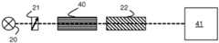
第一示例基于偏振测定方法,其中图2示出使用偏振测定正交检测的典型传感器的示意图,其中,静态光学相移偏置被引入在两个检测信道之间。如所示的组件是光源20、输入偏振器21、感测元件22(其在使用中将会暴露于被测对象)、第一分束器23-1、第二分束器23-2、四分之一波延迟器(QWR)24、第一输出偏振器25-1、第二输出偏振器25-2和3个光学功率检测器26-1,26-2,26-3。该波的束路径示出为一个或多个散列线。3个检测器连接至输出束路径:第一检测器26-1没有附接的偏振器,第二检测器26-2具有线性输出偏振器25-1,并且第三检测器26-3具有四分之一波延迟器24和线性输出偏振器25-2。在这3个检测器处测量的光学信号是分别高达一些比例常数:The first example is based on the polarimetry approach, where Figure 2 shows a schematic diagram of a typical sensor using polarimetric quadrature detection, where a static optical phase shift bias is introduced between the two detection channels. Components as shown are

其中I0代表由光源20发射的总功率,并且
在信号处理单元31的第一部分(或者相移检测单元)31-1中,组合至少一些测量的信号来导出代表相移的主值的第一测量。在信号处理单元31的第二部分31-2(或者对比度检测单元)中,组合至少一些测量的信号来导出代表互相关或者自相关函数A的第二测量。为此,存在多个信号处理方式。例如,信号处理单元31能够以下面的方式形成矢量或者复变量Y:In a first part (or phase shift detection unit) 31-1 of the


能够进一步示出的是,如由图2所代表的检测方案没有准确的90°相位偏置(尽管是优选的)也工作,并且仅要求具有两个具有除了0°或者180°的某个已知的相对相位差的偏振测定信道。确实,如果例如具有检测器26-3的第三检测器信道具有附加的相位偏移

其中Y的自变量和绝对值仍然产生相移主值和干扰对比度。在这种情况下,QWR元件24能够通过除了全波和半波延迟器以外的任何相位延迟器来替换。where the independent variable and absolute value of Y still produce the phase-shift principal value and the interference contrast. In this case, the
测量I0的另一个选项能够具有在如由检测器26-2和26-3所代表的两个偏振测定检测器信道的至少一个中从偏振分束器(替换偏振器25-1或者25-2)测量两个反相输出的检测器。两个反相输出的总和然后将会产生总光功率I0。还要注意,在其中总光功率是已知的和/或保持恒定,或者能够容易经由电子装置或者通过使用位于光学感测子系统之前的其他检测器来监控或控制的情况下,不需要I0测量。Another option for measuringI0 can have a beam splitter (replacing polarizer 25-1 or 25- 2) A detector measuring two out-of-phase outputs. The sum of the two inverted outputs will then yield the total optical power I0 . Note also that in cases where the total optical power is known and/or held constant, or can be easily monitored or controlled via electronics or by using other detectors located before the optical sensing subsystem, no I0 measurements.
作为同时测量相移主值和干扰对比度的方法的第二示例,图3示出使用有源相位调制方案的本发明的示例。示出的传感器使用调制相位检测(MPD)原理,通常实现在"非交互相位调制"方案并且通常被用于光纤陀螺仪和电流传感器中。如上文参考文献[9]引用的共同拥有的美国专利7911196描述例如结合电压感测元件(或者若干这类元件)、45°法拉第旋转器以及MPD调制和检测电子设备的电压传感器。重要的是注意,MPD技术先前仅被用来测量相移主值。但是如下文所示,相同的测量方案能够扩展至同时产生干扰对比度。As a second example of a method of simultaneously measuring the principal value of the phase shift and the interference contrast, Figure 3 shows an example of the present invention using an active phase modulation scheme. The sensor shown uses the Modulated Phase Detection (MPD) principle, typically implemented in a "non-reciprocal phase modulation" scheme and commonly used in fiber optic gyroscopes and current sensors. Commonly owned US Pat. No. 7,911,196, as cited in reference [9] above, describes, for example, a voltage sensor incorporating a voltage sensing element (or several such elements), a 45° Faraday rotator, and MPD modulation and detection electronics. It is important to note that the MPD technique has previously only been used to measure the principal value of the phase shift. However, as shown below, the same measurement scheme can be extended to generate interference contrast simultaneously.
如图3所示的使用MPD检测方案的传感器的基本组件(并且对于具有相同或者类似功能的组件,在适当的情况下使用与图2相同的数字)是光源20、输入偏振器21、感测元件22(其在使用中会暴露于被测对象)、输出偏振器25和检测器26。该波的束路径示出为一个或多个虚线。双折射相位调制器30也包含在束路径中。相位调制器30和检测器26通过信号处理单元31耦合,用于执行如下面描述的信号分析。The basic components of a sensor using the MPD detection scheme as shown in Figure 3 (and for components with the same or similar functionality, using the same numbers as in Figure 2 where appropriate) are a
双折射相位调制器30与感测媒介22光学串联连接,使得附加的光学相移调制β(t)能够增加至待测量的相移。检测器26在线性偏振器25之后测量调制的光学功率。调制的检测器信号能够写为:The

其中I0代表源的总功率,

如在上文图2的示例中,信号处理单元31的第一部分(或者相移检测单元)31-1分析检测的信号I(t),以导出代表相对相移


其中前3个谐波幅度Bk和相位


使用第一类Jk(β)的贝塞尔函数,谐波分量的符号能够通过将谐波分量的相位与激励波形的相位比较来确定。Using a Bessel function of the first kind ofJk (β), the sign of the harmonic component can be determined by comparing the phase of the harmonic component to the phase of the excitation waveform.
能够从上文代表形成矢量或者复数,其允许从检测的谐波幅度Bk导出相移主值


优选调制幅度是β = 1.84拉德,其中J1(β)具有其第一最大数;另一个优选幅度是β = 2.63拉德,其中J1(β)和J2(β)是相等的。但是,大体上,对于用来工作的MPD方法,相位调制幅度β能够为任意小。此外,例如为了稳定幅度的目的,已知的是调制幅度β也能够从测量谐波幅度来计算。代替正弦调制,可使用其他波形、具体来说是方波调制。开环MPD信号处理的另外细节能够见于参考文献[6、27]。A preferred modulation amplitude is β = 1.84 rad, where J1 (β) has its first maximum number; another preferred amplitude is β = 2.63 rad, where J1 (β) and J2 (β) are equal. In general, however, the phase modulation amplitude β can be arbitrarily small for the MPD method used to work. Furthermore, for example for the purpose of stabilizing the amplitude, it is known that the modulation amplitude β can also be calculated from the measured harmonic amplitudes. Instead of sinusoidal modulation, other waveforms, in particular square wave modulation, can be used. Additional details of open-loop MPD signal processing can be found in references [6, 27].
如早期描述,适当的明确测量范围处于其中互相关函数

如图4由一般检测单元41代表的检测方案能够是偏振测定方案或者如上述的MPD方案,或者同时检测相移主值和干扰对比度的任何其他检测方案。如已经结合图1B描述,应该选择静态元件40的组延迟偏置和光源20的相干时间,使得被测对象x的目标测量范围映射至包含在具有大斜率


如上所提及,如描述的去除周期方面的歧义性能够应用到许多类型的干涉测定传感器。然而,由于缺少可比较的备选方案,其特别适合于扩展DC电场或者电压传感器的测量范围,如例如参考文献[1]中描述的。As mentioned above, disambiguation in terms of periods as described can be applied to many types of interferometric sensors. However, due to the lack of comparable alternatives, it is particularly suitable for extending the measurement range of DC electric field or voltage sensors, as described for example in ref. [1].
在这些传感器中,低相干光源(例如SLED源、1310 nm的中心波长、40 nm的FWHM带宽)被用来产生干扰信号,其自相关从一个相周期到另一个相周期显著变化。电光晶体被用作感测媒介,以要测量的电压转换为晶体中正交偏振模式之间的相对相移。没有自然双折射的电光晶体(例如Bi4Ge3O12、BGO)是优选的。电光波导或者光纤也能够被用作电压感测媒介。BGO晶体(与[001]方向垂直切割)的端面电连接至提供电压降的电极。In these sensors, a low-coherence light source (e.g., SLED source, central wavelength of 1310 nm, FWHM bandwidth of 40 nm) is used to generate interfering signals whose autocorrelation varies significantly from one phase period to another. An electro-optic crystal is used as the sensing medium to translate the voltage to be measured into the relative phase shift between orthogonal polarization modes in the crystal. Electro-optic crystals without natural birefringence (eg Bi4Ge3O12, BGO) are preferred. Electro-optical waveguides or optical fibers can also be used as voltage sensing media. The end faces of the BGO crystal (cut perpendicular to the [001] direction) are electrically connected to electrodes that provide a voltage drop.
因此,与现有技术中发现的一些传感器设计相比,跨感测晶体应用全电压(而非其一小部分)。电压应用在晶体的纵向方向上,因此,测量在该方向上的电场的路径积分(即,应用的电压)。因此,电压测量独立于晶体中的内部电荷再分布。Thus, in contrast to some sensor designs found in the prior art, the full voltage (rather than a fraction of it) is applied across the sensing crystal. The voltage is applied in the longitudinal direction of the crystal, therefore, the path integral of the electric field in this direction (ie, the applied voltage) is measured. Therefore, the voltage measurement is independent of the internal charge redistribution in the crystal.
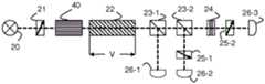
在电压的偏振测定检测器的示例中,图2和图4的元件被组合(并且因此在适当的情况下使用相同的数字),如图5所图示。In the example of a voltage polarimetry detector, the elements of FIGS. 2 and 4 are combined (and therefore use the same numbers where appropriate), as illustrated in FIG. 5 .
图5示出其中感测元件被用于传输的扩展范围的DC电压传感器的设计。3个检测器信道26-1、26-2和26-3分别产生总光功率和两个正交偏振测定信号,如上所述(参见等式[2])。具有静态相对组延迟的双折射晶体(例如结晶石英波板)作为组延迟偏置元件40,插入在输入偏振器21与第二分束器23-2之间,如上所论述。使用组延迟偏置元件40是优选的,但如果待测量的电压的极性是已知的并且因此,测量范围中的图1A和1B中的曲线12的斜率的符号是已知的,那么可能不总是被需要。如果电压极性是未知的,那么双折射晶体40用来在两个极性扩展明确的测量范围。如果采用具有自然双折射的电光晶体作为生成期望的组延迟偏置的感测元件22,那么也可以省略双折射晶体。为了减小组延迟偏置的温度小相关性,组延迟偏置元件40可以是复合光学器件,由两个晶体(其具有平行光轴,如果其热双折射系数是相反符号的话,或者其具有交换光轴,如果其热双折射系数是相同的符号的话)串联制成。另外,能够测量组延迟偏置元件的温度,由此,其温度相关的组延迟和相移变化能够在信号处理中被补偿。Figure 5 shows a design of an extended range DC voltage sensor in which the sensing element is used for transmission. The three detector channels 26-1, 26-2 and 26-3 generate the total optical power and two orthogonal polarimetric signals, respectively, as described above (see equation [2]). A birefringent crystal with static relative group retardation, such as a crystalline quartz waveplate, is inserted as group
输入偏振器21和两个输出偏振器25-1和25-2的轴以±45°对准,而组延迟偏置元件40和QWR24的轴与感测元件22的电光轴平行对准。在该示例中,被测对象x是BGO晶体的端面之间应用的电压V,其中[001]晶轴在光波传播的方向上取向。优选地,分束器应该相对于电光晶体轴与其轴以45°对准,以便使两个偏振波可能从分束器经历的任何可能的相移相等。例如来自分束器或者来自电光晶体的残留自然双折射的任何残留系统相移能够通过校准表征并且去掉。还能够通过将两个BGO晶体串联组合,其中反平行[001]轴和x/y轴相对彼此旋转90°,从而减少如果存在的BGO的残留双折射。在该布置中,电光相移进行合计,而本征双折射取消,引起更好的零点稳定性。The axes of
在图6中,描述与图5类似的设备,其中利用如结合等式[2]上文已经描述地那样测量总功率的不同的方式。仅使用一个无双折射的分束器23-2,并且具有检测器26-1和26-2的两个检测器信道连接至偏振分束器60的两个反相输出。总光学功率由检测器26-1和26-2处的功率的总和给出,而检测器26-1(或者26-2)和检测器26-3构成一对正交偏振测定信道。In Fig. 6, an apparatus similar to that of Fig. 5 is depicted, wherein a different way of measuring the total power is used as already described above in connection with equation [2]. Only one birefringence-free beam splitter 23-2 is used, and the two detector channels with detectors 26-1 and 26-2 are connected to the two opposite-phase outputs of
代替测量BGO晶体的输出端处的总光学功率,还能够监测光进入感测晶体之前的总光功率。甚至能够依赖光源20的内部监测器来跟踪功率变化或保持稳定的光学功率输出。然而,这类方案将不能够处理从光源到偏振测定检测器的路径中的光损耗变化,这在实际传感器中能够是重要的,尤其是如果光纤被用来将光从光源输送到感测晶体。Instead of measuring the total optical power at the output of the BGO crystal, it is also possible to monitor the total optical power before the light enters the sensing crystal. It is even possible to rely on an internal monitor of the
偏振测定电压传感器还能够以反射配置设计,其中,如由被测对象引起的电光相移将会加倍。图7A和7B示出了图示这种配置的示例,其中,反射光学器件70置于晶体的一端,并且所有其他光学元件位于另一端处。其他元件与参考上文图5时已经描述的元件相同或者类似。Polarimetry voltage sensors can also be designed in a reflective configuration, where the electro-optic phase shift, eg, caused by the object being measured, will be doubled. Figures 7A and 7B show examples illustrating such a configuration, where
反射光学器件70可以是平坦/弯曲反射镜、屋顶型反射镜、角锥棱镜反向反射器或者只是沉积在晶体端面上的反射薄膜涂层。反射光学器件处的反射应当理想地保存光的偏振状态,而没有旋转或偏振相关相移。来自反射的任何残留相移也能够通过校准来表征和去掉。优选地,光源和晶体的检测器端连接到地电位,并且反射器端连接到高压,以便将光源和检测器保持在地电位.The
图8和9图示与MPD方案结合的扩展范围的DC电压传感器的示例。如上所述(参见等式[4']),MPD方案是同时测量相移和干扰对比度的另一个方法。然而,透射配置中的基于MPD的电压传感器,与图3描绘的传感器的类似,不适合大多数实际应用,因为相位调制器30中的本征相移以及连接的偏振保持光纤通常对于温度和/或应力变化非常敏感。因此,透射的基于MPD的电压传感器的的输出容易受环境扰动影响。8 and 9 illustrate an example of an extended range DC voltage sensor combined with an MPD scheme. As mentioned above (see equation [4']), the MPD scheme is another method to measure phase shift and interference contrast simultaneously. However, an MPD-based voltage sensor in a transmissive configuration, similar to that of the sensor depicted in Figure 3, is not suitable for most practical applications because of the intrinsic phase shift in the
另一方面,能够基于交互光学设计来设计健壮的MPD传感器,由此,两个干扰波在环路中对向传播(例如在光纤陀螺仪的情况下),或者在具有交换的正交偏振的反射时折回(retrace)光路径(例如在反射光纤电流传感器的情况下)。在这类设计中,相位调制器的本征相移和互连的PM光纤沿着交互路径自动取消(并且因此,其温度相关性也一样),而相位调制和被测对象引起的相移加倍。如在导言中已经解释的,这经常被称为"非交互相位调制"。On the other hand, robust MPD sensors can be designed based on an interactive optical design, whereby two interfering waves propagate counter-propagating in the loop (as in the case of fiber optic gyroscopes, for example), or in a Retraces the optical path upon reflection (eg, in the case of a reflective fiber optic current sensor). In this type of design, the intrinsic phase shift of the phase modulator and the interconnected PM fibers are automatically canceled along the interaction path (and, therefore, their temperature dependence as well), while the phase modulation and the phase shift induced by the measured object are doubled . As already explained in the introduction, this is often referred to as "non-interactive phase modulation".
共同拥有的美国专利7911196(参考文献[9])描述结合电压感测元件(或者若干这类元件)、45°法拉第旋转器、MPD调制和检测电子设备的非交互相位调制电压传感器。由于相移的周期方面的歧义性问题,那个专利中的传感器仅能够明确地测量-π至+π范围的DC电光相移。然而,如上所示,除了相移以外,MPD信号处理方案还能够被扩展来也产生干扰对比度
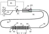
美国专利7911196中的所有实施例能够受益于本发明。为了证明本专利中的本发明如何能够扩展超出2π测量范围,对US 7911196中描述的示例的适当改编使用参考上文图3时已经描述的元件在图8中示出。在这里,低相干光源20和光电检测器26经由1x2光纤耦合器连接至感测元件22。光首先经过线性偏振器21,进入偏振保持(PM)光纤80,并且通过45°接头81耦合至光纤双折射相位调制器30的两个轴中。光然后耦合离开准直器82,经过45°法拉第旋转器83、组延迟偏置元件40并且进入感测元件22(沿着[001]轴的BGO晶体),其的端电连接至电压供应V。晶体端面能够涂有透明的导电电极层。光被感测媒介22的远端处的反射光学器件70依次反射回到感测媒介、组延迟偏置元件、法拉第旋转器和PM光纤中。反射光学器件可以是平坦/弯曲反射镜、屋顶型反射镜、角锥棱镜反向反射器或者只是沉积在晶体端面上的反射薄膜涂层。在这个示例中,反射光学器件处的反射应当理想地保存光的偏振状态,而没有旋转或偏振相关相移。All embodiments in US Pat. No. 7,911,196 can benefit from the present invention. To demonstrate how the invention in this patent can be extended beyond the 2π measurement range, a suitable adaptation of the example described in US 7911196 is shown in Figure 8 using elements already described with reference to Figure 3 above. Here, the low
充当静态组延迟偏置元件40的双折射晶体(诸如结晶石英波板)插入到法拉第旋转器83与反射光学器件70之间,以调整组延迟偏置,如上参考图1B时论述的。BGO晶体和双折射晶体的光学轴相对于PM光纤的轴以45°对准,从而通向准直器82。A birefringent crystal, such as a crystalline quartz waveplate, serving as static group
由于交互路径中的的2次45°法拉第旋转,干扰正交偏振的波随着其重新进入PM光纤和双折射相位调制器30而交换其偏振,由此取消关联的本征相移并且消除其温度相关性。返回路径上的45°接头81和偏振器21允许偏振波的相干混合,并且光电检测器26测量所得到的光功率。Due to the 2-fold 45° Faraday rotation in the interaction path, the wave interfering with the orthogonal polarization swaps its polarization as it re-enters the PM fiber and
信号处理和控制单元31控制相位调制波形,并且测量光电检测器处的光功率。其例如根据等式[4']描述的程序来计算相移主值和干扰对比度。最终,相移主值和干扰对比度组合成产生电压的明确测量。The signal processing and
例如来自分束器或者反射光学器件或者来自BGO晶体的残留自然双折射的任何残留系统相移能够通过校准表征并且去掉。Any residual system phase shift, eg from beam splitters or reflective optics or from residual natural birefringence of BGO crystals can be characterized and removed by calibration.
图9示出环路配置,其中,图8的反射光学器件70采用Y型相位调制器30以及另一个组准直器82'和法拉第旋转器83'来替换。由于法拉第旋转器83和83',波在两个对向传播方向上沿着感测媒介22的正交电光轴偏振,而其在PM光纤80中沿着相同的轴偏振。相对于图8的反射配置的优点在于:在光学组件的对准中存在更大的自由度,这可以简化从电光晶体回到PM光纤80的光耦合。图9设计的可能缺陷是组件的更大数量。Figure 9 shows a loop configuration in which the
虽然上面示出和描述本发明的一些优选的实施例,但要理解,本发明不限于此,而是可以在下面的权利要求的范围内另外以不同方式体现并且实施。While some preferred embodiments of the present invention have been shown and described above, it is to be understood that the present invention is not limited thereto, but may otherwise be embodied and carried out in various ways within the scope of the following claims.
虽然上述示例描述基于光学干涉仪的传感器,但应该领会,本发明能够应用于所有类型的干涉仪。例如,RF或者其他电磁辐射带中的干涉仪也能够受益于测量范围的相同的明确扩展。本发明也不限于电磁波。涉及波(无论它是声、密度还是其他类型的波)的任何干涉计也能够同样地获益。While the above examples describe optical interferometer based sensors, it should be appreciated that the present invention is applicable to all types of interferometers. For example, interferometers in RF or other electromagnetic radiation bands can also benefit from the same explicit extension of the measurement range. The present invention is also not limited to electromagnetic waves. Any interferometer involving waves (whether it be acoustic, density or other types of waves) can benefit equally.
低相干源能够是宽带宽的光源,或者是由在不同波长的多个源构成的组合源。其频谱的形状不重要。整个频带宽度的倒数应该在与传感器的期望的明确测量范围的宽度对应的组延迟跨度的相同阶。The low coherence source can be a wide bandwidth light source, or a combined source consisting of multiple sources at different wavelengths. The shape of its spectrum is not important. The reciprocal of the overall bandwidth should be in the same order as the group delay span corresponding to the width of the desired unambiguous measurement range of the sensor.
虽然DC电压传感器的设计作为示例来描述,但本发明也能够容易应用于光纤电流传感器、光纤陀螺仪或者其他类型的干涉测定传感器。然而,对于覆盖其中绝对零参考不可用的大范围的任何DC干涉测定传感器是尤其有利的。Although the design of a DC voltage sensor is described as an example, the invention can also be readily applied to fiber optic current sensors, fiber optic gyroscopes, or other types of interferometric sensors. However, it is especially advantageous for any DC interferometric sensor that covers a large range where absolute zero reference is not available.
参考文献references


Claims (26)


Applications Claiming Priority (3)
| Application Number | Priority Date | Filing Date | Title |
|---|---|---|---|
| EP14156090 | 2014-02-21 | ||
| EP14156090.4 | 2014-02-21 | ||
| PCT/EP2015/053513WO2015124676A1 (en) | 2014-02-21 | 2015-02-19 | Interferometric sensor |
Publications (2)
| Publication Number | Publication Date |
|---|---|
| CN105992934A CN105992934A (en) | 2016-10-05 |
| CN105992934Btrue CN105992934B (en) | 2020-09-22 |
Family
ID=50137557
Family Applications (1)
| Application Number | Title | Priority Date | Filing Date |
|---|---|---|---|
| CN201580009630.8AExpired - Fee RelatedCN105992934B (en) | 2014-02-21 | 2015-02-19 | Interferometric sensor |
Country Status (7)
| Country | Link |
|---|---|
| US (1) | US10725073B2 (en) |
| EP (1) | EP3108212B1 (en) |
| CN (1) | CN105992934B (en) |
| AU (1) | AU2015220811C1 (en) |
| ES (1) | ES2662124T3 (en) |
| RU (1) | RU2677126C2 (en) |
| WO (1) | WO2015124676A1 (en) |
Families Citing this family (12)
| Publication number | Priority date | Publication date | Assignee | Title |
|---|---|---|---|---|
| CN105953817B (en)* | 2016-04-26 | 2018-10-26 | 哈尔滨工程大学 | A kind of assemble method of optical fibre gyro core sensitivity light path |
| US10712180B2 (en)* | 2016-08-11 | 2020-07-14 | The Charles Stark Draper Laboratory, Inc. | Segmented poled optical fiber for fiber optic sensor and phased array |
| ES2741848T3 (en) | 2016-09-02 | 2020-02-12 | Abb Schweiz Ag | Interferometric voltage sensor with error compensation |
| EP3290870B1 (en) | 2016-09-02 | 2019-03-13 | ABB Schweiz AG | Closed-loop interferometric sensor using loop gain for determining interference contrast |
| EP3730897A1 (en) | 2019-04-25 | 2020-10-28 | Nokia Technologies Oy | Apparatus, systems and methods for detecting light |
| JP7252876B2 (en)* | 2019-10-16 | 2023-04-05 | 株式会社アドバンテスト | Optical test equipment |
| CN111157100B (en)* | 2020-01-02 | 2022-05-20 | 河海大学常州校区 | All-fiber sensing positioning system and positioning method based on feedback |
| CN111474553B (en)* | 2020-06-22 | 2020-11-27 | 深圳市汇顶科技股份有限公司 | Time-of-flight ranging method and device |
| WO2021258236A1 (en)* | 2020-06-22 | 2021-12-30 | 深圳市汇顶科技股份有限公司 | Time of flight ranging method and apparatus |
| DE102020120533A1 (en) | 2020-08-04 | 2022-02-10 | Technische Universität Dresden | Device and method for determining a measured value |
| KR102251284B1 (en)* | 2020-11-27 | 2021-05-12 | 국방과학연구소 | Apparatus and method for measuring voltage using an optical element |
| WO2022155270A1 (en)* | 2021-01-12 | 2022-07-21 | The Board Of Trustees Of The University Of Illinois | Multiphase optical coherence microscopy imaging |
Citations (6)
| Publication number | Priority date | Publication date | Assignee | Title |
|---|---|---|---|---|
| WO1994018523A1 (en)* | 1993-02-01 | 1994-08-18 | Zygo Corporation | Method and apparatus for the rapid acquisition of data in coherence scanning interferometry |
| DE19701221C1 (en)* | 1997-01-16 | 1998-04-23 | Abb Research Ltd | Method of temperature compensation of measurement signals of fibre optical sensors |
| WO2003093759A2 (en)* | 2002-05-02 | 2003-11-13 | Zygo Corporation | Phase gap analysis for scanning interferometry |
| WO2011069558A1 (en)* | 2009-12-11 | 2011-06-16 | Abb Research Ltd | Fiber-optic current sensing using a sensor with exchangeable sub-modules |
| CN102520374A (en)* | 2011-11-29 | 2012-06-27 | 北京航空航天大学 | Optical fiber magnetic field sensor digital closed loop detection device with double modulation characteristics |
| CN102914256A (en)* | 2012-09-29 | 2013-02-06 | 哈尔滨工程大学 | Synchronous phase shifting interference detection device based on orthogonal double grating and detection method |
Family Cites Families (16)
| Publication number | Priority date | Publication date | Assignee | Title |
|---|---|---|---|---|
| DE3044183A1 (en) | 1980-11-24 | 1982-06-24 | Reinhard Dipl.-Phys. Dr. 7250 Leonberg Ulrich | METHOD FOR OPTICALLY MEASURING LENGTHS AND LENGTH CHANGES AND ARRANGEMENT FOR IMPLEMENTING THE METHOD |
| US4904931A (en) | 1988-09-28 | 1990-02-27 | Westinghouse Electric Corp. | Electro-optical voltage measuring system incorporating a method and apparatus to derive the measured voltage waveform from two phase shifted electrical signals |
| US5001419A (en) | 1988-09-28 | 1991-03-19 | Abb Power T & D Company Inc. | Method of deriving an AC waveform from two phase shifted electrical signals |
| GB8903725D0 (en) | 1989-02-18 | 1989-04-05 | Cambridge Consultants | Coherent tracking sensor |
| RU2032181C1 (en)* | 1991-02-05 | 1995-03-27 | Киселев Владимир Васильевич | Fiber-optic electric-field strength and voltage meter |
| US5271034A (en)* | 1991-08-26 | 1993-12-14 | Avion Systems, Inc. | System and method for receiving and decoding global positioning satellite signals |
| DE4416298A1 (en) | 1994-05-09 | 1995-11-16 | Abb Research Ltd | Method and device for optically determining a physical quantity |
| CA2261901A1 (en) | 1996-08-01 | 1998-02-12 | Siemens Aktiengesellschaft | Method and arrangement for optically detecting an electrical variable |
| US6301400B1 (en)* | 1998-11-12 | 2001-10-09 | Nxtphase Technologies Srl | Fiber optic current sensor having rotation immunity |
| US6429939B1 (en) | 2000-07-13 | 2002-08-06 | Kvh Industries, Inc. | DSP signal processing for open loop fiber optic sensors |
| DE10039455A1 (en) | 2000-08-12 | 2002-02-21 | Abb Patent Gmbh | DC converter |
| US6946827B2 (en)* | 2001-11-13 | 2005-09-20 | Nxtphase T & D Corporation | Optical electric field or voltage sensing system |
| US7355716B2 (en)* | 2002-01-24 | 2008-04-08 | The General Hospital Corporation | Apparatus and method for ranging and noise reduction of low coherence interferometry LCI and optical coherence tomography OCT signals by parallel detection of spectral bands |
| KR101006422B1 (en)* | 2005-01-20 | 2011-01-06 | 지고 코포레이션 | Interferometer to determine the characteristics of the object surface |
| EP2095135B1 (en) | 2006-12-22 | 2015-11-04 | ABB Research Ltd. | Optical voltage sensor |
| JP5437085B2 (en)* | 2010-01-06 | 2014-03-12 | 株式会社ミツトヨ | Optical fiber type magnetic field sensor |
- 2015
- 2015-02-19CNCN201580009630.8Apatent/CN105992934B/ennot_activeExpired - Fee Related
- 2015-02-19ESES15705315.8Tpatent/ES2662124T3/enactiveActive
- 2015-02-19AUAU2015220811Apatent/AU2015220811C1/ennot_activeCeased
- 2015-02-19RURU2016137476Apatent/RU2677126C2/enactive
- 2015-02-19WOPCT/EP2015/053513patent/WO2015124676A1/enactiveApplication Filing
- 2015-02-19EPEP15705315.8Apatent/EP3108212B1/ennot_activeNot-in-force
- 2016
- 2016-08-22USUS15/243,713patent/US10725073B2/enactiveActive
Patent Citations (6)
| Publication number | Priority date | Publication date | Assignee | Title |
|---|---|---|---|---|
| WO1994018523A1 (en)* | 1993-02-01 | 1994-08-18 | Zygo Corporation | Method and apparatus for the rapid acquisition of data in coherence scanning interferometry |
| DE19701221C1 (en)* | 1997-01-16 | 1998-04-23 | Abb Research Ltd | Method of temperature compensation of measurement signals of fibre optical sensors |
| WO2003093759A2 (en)* | 2002-05-02 | 2003-11-13 | Zygo Corporation | Phase gap analysis for scanning interferometry |
| WO2011069558A1 (en)* | 2009-12-11 | 2011-06-16 | Abb Research Ltd | Fiber-optic current sensing using a sensor with exchangeable sub-modules |
| CN102520374A (en)* | 2011-11-29 | 2012-06-27 | 北京航空航天大学 | Optical fiber magnetic field sensor digital closed loop detection device with double modulation characteristics |
| CN102914256A (en)* | 2012-09-29 | 2013-02-06 | 哈尔滨工程大学 | Synchronous phase shifting interference detection device based on orthogonal double grating and detection method |
Also Published As
| Publication number | Publication date |
|---|---|
| RU2677126C2 (en) | 2019-01-15 |
| AU2015220811A1 (en) | 2016-10-13 |
| US20160356823A1 (en) | 2016-12-08 |
| ES2662124T3 (en) | 2018-04-05 |
| EP3108212B1 (en) | 2017-12-13 |
| AU2015220811B2 (en) | 2019-07-04 |
| RU2016137476A3 (en) | 2018-11-12 |
| US10725073B2 (en) | 2020-07-28 |
| EP3108212A1 (en) | 2016-12-28 |
| WO2015124676A1 (en) | 2015-08-27 |
| AU2015220811C1 (en) | 2019-11-28 |
| CN105992934A (en) | 2016-10-05 |
| RU2016137476A (en) | 2018-03-27 |
Similar Documents
| Publication | Publication Date | Title |
|---|---|---|
| CN105992934B (en) | Interferometric sensor | |
| EP2333498B1 (en) | Sagnac interferometer-type fiber-optic current sensor | |
| CN101886925B (en) | Multi-wavelength interference type optical fiber gyro based on carrier modulation | |
| JP2000515979A (en) | Optical fiber device and method for precision current sensing | |
| JPH1090175A (en) | Apparatus and method for measuring fluctuation in gas refractive index in measurement path | |
| KR101978444B1 (en) | Optical fiber Sagnac interferometer using a polarizing beam splitter | |
| US10302411B2 (en) | Closed-loop interferometric sensor using loop gain for determining interference contrast | |
| WO2018014325A1 (en) | Phase modulation-based dual-laser single-frequency interferometric nanometer displacement measurement device and method | |
| CN106062506B (en) | Interferometric sensor | |
| CN103292976A (en) | Interferometry-based optical fiber Verdet constant measuring system | |
| Zheng et al. | Influences of optical-spectrum errors on excess relative intensity noise in a fiber-optic gyroscope | |
| CN103542870B (en) | Ac modulation type low coherence interference demodulating system | |
| Petrov et al. | Fiber-optic polarization interferometric sensor for precise electric field measurements | |
| Li et al. | IFOG based on rhombic optical path difference bias configuration for high-frequency angular vibration measurement | |
| CN106796125B (en) | Interferometric sensor with differential modulation phase detection | |
| RU2682981C1 (en) | Demodulation method of fiber optic current sensor signal | |
| Bohnert et al. | Fiber-optic voltage sensor using fiber gyro technology | |
| Jones | Interferometry and polarimetry for optical sensing | |
| Liokumovich et al. | Fiber-optic polarization interferometer with an additional phase modulation for electric field measurements | |
| Wildermuth et al. | Interrogation of a birefringent fiber sensor by nonreciprocal phase modulation | |
| RU2433414C1 (en) | Fibre-optic current sensor | |
| Feng et al. | Influences of imperfect polarization induced effects to the quasi-reciprocal reflective optical voltage sensor | |
| Kublanova et al. | Study of an interferometric fiber-optic gyroscope with a birefringence modulator | |
| RU2579541C1 (en) | Voltage meter based on pockels effect | |
| Zheng | The new-conceptual fiber-optic gyroscope |
Legal Events
| Date | Code | Title | Description |
|---|---|---|---|
| C06 | Publication | ||
| PB01 | Publication | ||
| C41 | Transfer of patent application or patent right or utility model | ||
| TA01 | Transfer of patent application right | Effective date of registration:20161115 Address after:Baden, Switzerland Applicant after:ABB Switzerland Co.,Ltd. Address before:Baden, Switzerland Applicant before:Asea Brown Boveri Ltd. | |
| SE01 | Entry into force of request for substantive examination | ||
| SE01 | Entry into force of request for substantive examination | ||
| TA01 | Transfer of patent application right | Effective date of registration:20200602 Address after:Baden, Switzerland Applicant after:ABB grid Switzerland AG Address before:Baden, Switzerland Applicant before:ABB Switzerland Co.,Ltd. | |
| TA01 | Transfer of patent application right | ||
| GR01 | Patent grant | ||
| GR01 | Patent grant | ||
| CF01 | Termination of patent right due to non-payment of annual fee | Granted publication date:20200922 Termination date:20220219 | |
| CF01 | Termination of patent right due to non-payment of annual fee |