CN105741799B - Display device and method for processing data thereof - Google Patents
Display device and method for processing data thereofDownload PDFInfo
- Publication number
- CN105741799B CN105741799BCN201510983233.2ACN201510983233ACN105741799BCN 105741799 BCN105741799 BCN 105741799BCN 201510983233 ACN201510983233 ACN 201510983233ACN 105741799 BCN105741799 BCN 105741799B
- Authority
- CN
- China
- Prior art keywords
- pixels
- pixel
- data
- pattern
- gate line
- Prior art date
- Legal status (The legal status is an assumption and is not a legal conclusion. Google has not performed a legal analysis and makes no representation as to the accuracy of the status listed.)
- Expired - Fee Related
Links
- 238000000034methodMethods0.000titleclaimsabstractdescription19
- 239000004973liquid crystal related substanceSubstances0.000claimsabstractdescription88
- 230000000052comparative effectEffects0.000description18
- 101100299505Schizosaccharomyces pombe (strain 972 / ATCC 24843) ptn1 geneProteins0.000description17
- 239000003086colorantSubstances0.000description15
- 239000000758substrateSubstances0.000description14
- 230000004044responseEffects0.000description12
- 239000003990capacitorSubstances0.000description9
- 238000010586diagramMethods0.000description6
- 239000010409thin filmSubstances0.000description6
- 230000008878couplingEffects0.000description1
- 238000010168coupling processMethods0.000description1
- 238000005859coupling reactionMethods0.000description1
- 230000000694effectsEffects0.000description1
- 230000005684electric fieldEffects0.000description1
- 238000007689inspectionMethods0.000description1
- 238000012423maintenanceMethods0.000description1
- 238000012986modificationMethods0.000description1
- 230000004048modificationEffects0.000description1
- 230000002093peripheral effectEffects0.000description1
- 238000002834transmittanceMethods0.000description1
Images


Classifications
- G—PHYSICS
- G09—EDUCATION; CRYPTOGRAPHY; DISPLAY; ADVERTISING; SEALS
- G09G—ARRANGEMENTS OR CIRCUITS FOR CONTROL OF INDICATING DEVICES USING STATIC MEANS TO PRESENT VARIABLE INFORMATION
- G09G3/00—Control arrangements or circuits, of interest only in connection with visual indicators other than cathode-ray tubes
- G09G3/20—Control arrangements or circuits, of interest only in connection with visual indicators other than cathode-ray tubes for presentation of an assembly of a number of characters, e.g. a page, by composing the assembly by combination of individual elements arranged in a matrix no fixed position being assigned to or needed to be assigned to the individual characters or partial characters
- G09G3/34—Control arrangements or circuits, of interest only in connection with visual indicators other than cathode-ray tubes for presentation of an assembly of a number of characters, e.g. a page, by composing the assembly by combination of individual elements arranged in a matrix no fixed position being assigned to or needed to be assigned to the individual characters or partial characters by control of light from an independent source
- G09G3/36—Control arrangements or circuits, of interest only in connection with visual indicators other than cathode-ray tubes for presentation of an assembly of a number of characters, e.g. a page, by composing the assembly by combination of individual elements arranged in a matrix no fixed position being assigned to or needed to be assigned to the individual characters or partial characters by control of light from an independent source using liquid crystals
- G09G3/3603—Control arrangements or circuits, of interest only in connection with visual indicators other than cathode-ray tubes for presentation of an assembly of a number of characters, e.g. a page, by composing the assembly by combination of individual elements arranged in a matrix no fixed position being assigned to or needed to be assigned to the individual characters or partial characters by control of light from an independent source using liquid crystals with thermally addressed liquid crystals
- G—PHYSICS
- G09—EDUCATION; CRYPTOGRAPHY; DISPLAY; ADVERTISING; SEALS
- G09G—ARRANGEMENTS OR CIRCUITS FOR CONTROL OF INDICATING DEVICES USING STATIC MEANS TO PRESENT VARIABLE INFORMATION
- G09G3/00—Control arrangements or circuits, of interest only in connection with visual indicators other than cathode-ray tubes
- G09G3/20—Control arrangements or circuits, of interest only in connection with visual indicators other than cathode-ray tubes for presentation of an assembly of a number of characters, e.g. a page, by composing the assembly by combination of individual elements arranged in a matrix no fixed position being assigned to or needed to be assigned to the individual characters or partial characters
- G09G3/34—Control arrangements or circuits, of interest only in connection with visual indicators other than cathode-ray tubes for presentation of an assembly of a number of characters, e.g. a page, by composing the assembly by combination of individual elements arranged in a matrix no fixed position being assigned to or needed to be assigned to the individual characters or partial characters by control of light from an independent source
- G09G3/36—Control arrangements or circuits, of interest only in connection with visual indicators other than cathode-ray tubes for presentation of an assembly of a number of characters, e.g. a page, by composing the assembly by combination of individual elements arranged in a matrix no fixed position being assigned to or needed to be assigned to the individual characters or partial characters by control of light from an independent source using liquid crystals
- G09G3/3607—Control arrangements or circuits, of interest only in connection with visual indicators other than cathode-ray tubes for presentation of an assembly of a number of characters, e.g. a page, by composing the assembly by combination of individual elements arranged in a matrix no fixed position being assigned to or needed to be assigned to the individual characters or partial characters by control of light from an independent source using liquid crystals for displaying colours or for displaying grey scales with a specific pixel layout, e.g. using sub-pixels
- G—PHYSICS
- G09—EDUCATION; CRYPTOGRAPHY; DISPLAY; ADVERTISING; SEALS
- G09G—ARRANGEMENTS OR CIRCUITS FOR CONTROL OF INDICATING DEVICES USING STATIC MEANS TO PRESENT VARIABLE INFORMATION
- G09G3/00—Control arrangements or circuits, of interest only in connection with visual indicators other than cathode-ray tubes
- G09G3/20—Control arrangements or circuits, of interest only in connection with visual indicators other than cathode-ray tubes for presentation of an assembly of a number of characters, e.g. a page, by composing the assembly by combination of individual elements arranged in a matrix no fixed position being assigned to or needed to be assigned to the individual characters or partial characters
- G09G3/34—Control arrangements or circuits, of interest only in connection with visual indicators other than cathode-ray tubes for presentation of an assembly of a number of characters, e.g. a page, by composing the assembly by combination of individual elements arranged in a matrix no fixed position being assigned to or needed to be assigned to the individual characters or partial characters by control of light from an independent source
- G09G3/36—Control arrangements or circuits, of interest only in connection with visual indicators other than cathode-ray tubes for presentation of an assembly of a number of characters, e.g. a page, by composing the assembly by combination of individual elements arranged in a matrix no fixed position being assigned to or needed to be assigned to the individual characters or partial characters by control of light from an independent source using liquid crystals
- G09G3/3611—Control of matrices with row and column drivers
- G09G3/3614—Control of polarity reversal in general
- G—PHYSICS
- G09—EDUCATION; CRYPTOGRAPHY; DISPLAY; ADVERTISING; SEALS
- G09G—ARRANGEMENTS OR CIRCUITS FOR CONTROL OF INDICATING DEVICES USING STATIC MEANS TO PRESENT VARIABLE INFORMATION
- G09G3/00—Control arrangements or circuits, of interest only in connection with visual indicators other than cathode-ray tubes
- G09G3/20—Control arrangements or circuits, of interest only in connection with visual indicators other than cathode-ray tubes for presentation of an assembly of a number of characters, e.g. a page, by composing the assembly by combination of individual elements arranged in a matrix no fixed position being assigned to or needed to be assigned to the individual characters or partial characters
- G09G3/34—Control arrangements or circuits, of interest only in connection with visual indicators other than cathode-ray tubes for presentation of an assembly of a number of characters, e.g. a page, by composing the assembly by combination of individual elements arranged in a matrix no fixed position being assigned to or needed to be assigned to the individual characters or partial characters by control of light from an independent source
- G09G3/36—Control arrangements or circuits, of interest only in connection with visual indicators other than cathode-ray tubes for presentation of an assembly of a number of characters, e.g. a page, by composing the assembly by combination of individual elements arranged in a matrix no fixed position being assigned to or needed to be assigned to the individual characters or partial characters by control of light from an independent source using liquid crystals
- G09G3/3611—Control of matrices with row and column drivers
- G09G3/3648—Control of matrices with row and column drivers using an active matrix
- G—PHYSICS
- G09—EDUCATION; CRYPTOGRAPHY; DISPLAY; ADVERTISING; SEALS
- G09G—ARRANGEMENTS OR CIRCUITS FOR CONTROL OF INDICATING DEVICES USING STATIC MEANS TO PRESENT VARIABLE INFORMATION
- G09G2300/00—Aspects of the constitution of display devices
- G09G2300/04—Structural and physical details of display devices
- G09G2300/0421—Structural details of the set of electrodes
- G09G2300/0426—Layout of electrodes and connections
- G—PHYSICS
- G09—EDUCATION; CRYPTOGRAPHY; DISPLAY; ADVERTISING; SEALS
- G09G—ARRANGEMENTS OR CIRCUITS FOR CONTROL OF INDICATING DEVICES USING STATIC MEANS TO PRESENT VARIABLE INFORMATION
- G09G2300/00—Aspects of the constitution of display devices
- G09G2300/04—Structural and physical details of display devices
- G09G2300/0439—Pixel structures
- G09G2300/0452—Details of colour pixel setup, e.g. pixel composed of a red, a blue and two green components
- G—PHYSICS
- G09—EDUCATION; CRYPTOGRAPHY; DISPLAY; ADVERTISING; SEALS
- G09G—ARRANGEMENTS OR CIRCUITS FOR CONTROL OF INDICATING DEVICES USING STATIC MEANS TO PRESENT VARIABLE INFORMATION
- G09G2320/00—Control of display operating conditions
- G09G2320/02—Improving the quality of display appearance
- G09G2320/0209—Crosstalk reduction, i.e. to reduce direct or indirect influences of signals directed to a certain pixel of the displayed image on other pixels of said image, inclusive of influences affecting pixels in different frames or fields or sub-images which constitute a same image, e.g. left and right images of a stereoscopic display
- G—PHYSICS
- G09—EDUCATION; CRYPTOGRAPHY; DISPLAY; ADVERTISING; SEALS
- G09G—ARRANGEMENTS OR CIRCUITS FOR CONTROL OF INDICATING DEVICES USING STATIC MEANS TO PRESENT VARIABLE INFORMATION
- G09G2320/00—Control of display operating conditions
- G09G2320/02—Improving the quality of display appearance
- G09G2320/0233—Improving the luminance or brightness uniformity across the screen
Landscapes
- Engineering & Computer Science (AREA)
- Chemical & Material Sciences (AREA)
- Crystallography & Structural Chemistry (AREA)
- Physics & Mathematics (AREA)
- Computer Hardware Design (AREA)
- General Physics & Mathematics (AREA)
- Theoretical Computer Science (AREA)
- Control Of Indicators Other Than Cathode Ray Tubes (AREA)
- Liquid Crystal Display Device Control (AREA)
Abstract
Translated fromChinese
Description
Translated fromChinese相关申请的交叉引用CROSS-REFERENCE TO RELATED APPLICATIONS
本申请要求在2014年12月30日提交的韩国专利申请第10-2014-0194159号的优先权,其内容在此通过引用被整体合并于此。This application claims priority from Korean Patent Application No. 10-2014-0194159 filed on December 30, 2014, the contents of which are hereby incorporated by reference in their entirety.
技术领域technical field
本公开涉及显示装置和用于显示装置的处理数据的方法。更具体地,本公开涉及以反转驱动方式驱动的显示装置和用于显示装置的处理数据的方法。The present disclosure relates to a display device and a method of processing data for the display device. More particularly, the present disclosure relates to a display device driven in an inversion driving manner and a method of processing data for the display device.
背景技术Background technique
液晶显示器在置于两个基板之间的液晶层中形成电场并且改变液晶层的液晶分子的对准以控制穿过液晶层的光的透过率,并且因而通过液晶显示器来显示期望的图像。The liquid crystal display forms an electric field in a liquid crystal layer interposed between two substrates and changes the alignment of liquid crystal molecules of the liquid crystal layer to control the transmittance of light passing through the liquid crystal layer, and thus displays a desired image through the liquid crystal display.
根据施加到数据线的数据电压的极性,驱动液晶显示器的方法被分类为行反转方法、列反转方法和点反转方法。行反转方法每个像素行地将施加到数据线的图像数据的极性反转,列反转方法每个像素列地将施加到数据线的图像的极性反转,并且点反转方法每个像素行和每个像素列地将施加到数据线的图像数据的极性反转。Methods of driving liquid crystal displays are classified into row inversion methods, column inversion methods, and dot inversion methods according to polarities of data voltages applied to data lines. The row inversion method inverts the polarity of the image data applied to the data line per pixel row, the column inversion method inverts the polarity of the image applied to the data line per pixel column, and the dot inversion method Each pixel row and each pixel column reverses the polarity of the image data applied to the data lines.
通常,显示装置使用红色、绿色和蓝色的三原色来显示色彩。因此,显示装置包括分别与红色、绿色和蓝色色彩相对应的子像素。近年来,已经开发了使用红色、绿色、蓝色和其他原色来显示色彩的显示装置。作为其他原色,使用品红色、青色、黄色和白色色彩中的一个或多个。此外,为了改善图像的亮度,已经建议了包括红色、蓝色、绿色和白色子像素的显示装置。为此,来自外部源的红色、绿色和蓝色图像信号在被转换为红色、绿色、蓝色和白色数据信号之后被施加到显示面板。Generally, display devices display colors using three primary colors of red, green, and blue. Thus, the display device includes sub-pixels corresponding to red, green and blue colors, respectively. In recent years, display devices that display colors using red, green, blue, and other primary colors have been developed. As other primary colors, one or more of magenta, cyan, yellow, and white colors are used. Furthermore, in order to improve the brightness of an image, display devices including red, blue, green and white sub-pixels have been proposed. To this end, red, green and blue image signals from an external source are applied to the display panel after being converted into red, green, blue and white data signals.
发明内容SUMMARY OF THE INVENTION
本公开提供能够防止出现单线串扰(one-line crosstalk)的显示装置。The present disclosure provides a display device capable of preventing occurrence of one-line crosstalk.
本公开提供一种显示装置的处理数据的方法。The present disclosure provides a method of processing data of a display device.
本发明构思的实施例提供一种显示装置,包括液晶面板、栅极驱动器、数据驱动器和定时控制器。液晶面板包括在第一方向上延伸的多个栅极线、在与第一方向交叉的第二方向上延伸的多个数据线、和连接到栅极线和数据线的多个像素。Embodiments of the inventive concept provide a display device including a liquid crystal panel, a gate driver, a data driver, and a timing controller. The liquid crystal panel includes a plurality of gate lines extending in a first direction, a plurality of data lines extending in a second direction crossing the first direction, and a plurality of pixels connected to the gate lines and the data lines.
栅极驱动器向栅极线施加栅极信号,并且数据驱动器向数据线施加数据电压。The gate driver applies gate signals to the gate lines, and the data driver applies data voltages to the data lines.
定时控制器接收控制信号和图像数据,以向栅极驱动器施加栅极控制信号并且向数据驱动器施加数据控制信号。The timing controller receives the control signal and the image data to apply the gate control signal to the gate driver and the data control signal to the data driver.
像素包括在第二方向上彼此相邻的、布置在第h(h是自然数)行中的像素和布置在第h+1行中的像素,使得第k+1(k是自然数)栅极线被置于在布置在第h行中的像素和布置在第h+1行中的像素之间。The pixels include pixels arranged in the h-th (h is a natural number) row and pixels arranged in the h+1-th row, which are adjacent to each other in the second direction, such that the k+1-th (k is a natural number) gate line is placed between the pixel arranged in the h-th row and the pixel arranged in the h+1-th row.
布置在第h行中的像素之中的显示第一色彩并且连接到第k+1栅极线的第一像素与布置在第h+1行中的像素之中的显示第一色彩并且连接到第k+1栅极线的第二像素间隔开,并且接收具有与施加到第二像素的数据电压的极性不同的极性的数据电压。The first pixel arranged in the h-th row displays the first color and is connected to the k+1-th gate line and the pixel arranged in the h+1-th row displays the first color and is connected to The second pixel of the k+1 th gate line is spaced apart and receives a data voltage having a polarity different from that of the data voltage applied to the second pixel.
图像数据包括在第一像素的至少一部分中显示的第一像素数据和在第二像素的至少一部分中显示的第二像素数据。The image data includes first pixel data displayed in at least a portion of the first pixels and second pixel data displayed in at least a portion of the second pixels.
当第一像素数据具有第一灰度值并且第二像素数据具有不同于第一灰度值的第二灰度值时,定时控制器调整第一和第二像素数据以允许第一和第二像素数据具有第一和第二灰度值之间的灰度值。When the first pixel data has a first grayscale value and the second pixel data has a second grayscale value different from the first grayscale value, the timing controller adjusts the first and second pixel data to allow the first and second grayscale values The pixel data has grayscale values between the first and second grayscale values.
定时控制器调整第一像素数据以生成具有不同于第一和第二灰度值的第三灰度值的第一调整后像素数据并且调整第二像素数据以生成具有第三灰度值的第二调整后像素数据。The timing controller adjusts the first pixel data to generate first adjusted pixel data having a third grayscale value different from the first and second grayscale values and adjusts the second pixel data to generate a third grayscale value having the third grayscale value. 2. Adjusted pixel data.
第三灰度值对应于第一和第二灰度值之和的一半。The third grayscale value corresponds to half the sum of the first and second grayscale values.
定时控制器包括图案分析部分、调整确定部分和数据调整部分。图案分析部分分析图像数据的图案并且确定在第一方向上延伸的图案的边界是否被置于第一和第二像素之间。The timing controller includes a pattern analysis section, an adjustment determination section, and a data adjustment section. The pattern analysis section analyzes the pattern of the image data and determines whether a boundary of the pattern extending in the first direction is placed between the first and second pixels.
在本发明构思的实施例中,调整确定部分确定显示图案的第一像素的数量或显示图案的第二像素的数量是否等于或大于参考数量。In an embodiment of the present inventive concept, the adjustment determination section determines whether the number of first pixels of the display pattern or the number of second pixels of the display pattern is equal to or greater than a reference number.
在本发明构思的实施例中,调整确定部分确定显示图案的第一像素的灰度电压之和或显示图案的第二像素的灰度电压之和是否等于或大于参考电压。In an embodiment of the present inventive concept, the adjustment determination part determines whether the sum of the gray voltages of the first pixels of the display pattern or the sum of the gray voltages of the second pixels of the display pattern is equal to or greater than the reference voltage.
数据调整部分调整第一和第二像素数据。The data adjustment section adjusts the first and second pixel data.
当在图案的第一方向上延伸的边界被置于第一和第二像素之间并且显示图案的第一像素的数量或显示图案的第二像素的数量等于或大于参考数量时,数据调整部分调整第一和第二像素数据。When the boundary extending in the first direction of the pattern is placed between the first and second pixels and the number of the first pixels of the display pattern or the number of the second pixels of the display pattern is equal to or greater than the reference number, the data adjustment section Adjust the first and second pixel data.
当在图案的第一方向上延伸的边界没有被置于第一和第二像素之间或者当显示图案的第一像素的数量或显示图案的第二像素的数量小于参考数量时,数据调整部分不调整第一和第二像素数据。When the boundary extending in the first direction of the pattern is not placed between the first and second pixels or when the number of the first pixels of the display pattern or the number of the second pixels of the display pattern is less than the reference number, the data adjustment section The first and second pixel data are not adjusted.
当第一灰度值是非零并且第二灰度值是零时,调整确定部分检查显示图案的第一像素的数量是否等于或大于参考数量,并且当第二灰度值是非零并且第一灰度值是零时,调整确定部分检查显示图案的第二像素的数量是否等于或大于参考数量。When the first grayscale value is non-zero and the second grayscale value is zero, the adjustment determination section checks whether the number of first pixels of the display pattern is equal to or greater than the reference number, and when the second grayscale value is nonzero and the first grayscale value is When the degree value is zero, the adjustment determination section checks whether the number of the second pixels of the display pattern is equal to or greater than the reference number.
第一色彩是红色、绿色、蓝色或白色色彩。The first color is a red, green, blue or white color.
布置在第h行中的像素包括在第一方向上顺序地布置的第一像素组和第二像素组,布置在第h+1行中的像素包括在第一方向上顺序地布置的第三像素组和第四像素组,并且第一、第二、第三和第四像素组中的每一个包括偶数个像素。The pixels arranged in the h-th row include a first pixel group and a second pixel group sequentially arranged in the first direction, and the pixels arranged in the h+1-th row include a third pixel group arranged sequentially in the first direction A pixel group and a fourth pixel group, and each of the first, second, third and fourth pixel groups includes an even number of pixels.
第一和第四像素组中的每一个包括红色像素、绿色像素、蓝色像素和白色像素中的两种像素,并且第二和第三像素组中的每一个包括红色像素、绿色像素、蓝色像素和白色像素中的另外两种像素。Each of the first and fourth pixel groups includes two types of red pixels, green pixels, blue pixels, and white pixels, and each of the second and third pixel groups includes red pixels, green pixels, blue pixels The other two types of pixels are color pixels and white pixels.
当第一像素被包括在布置在第2u-1列中的像素中时,第二像素被包括在布置在第2u+1(u是自然数)列中的像素中,并且当第一像素被包括在布置在第2u列中的像素中时,第二像素被包括在布置在第2u+2列中的像素中。When the first pixel is included in the pixels arranged in the 2u-1th column, the second pixel is included in the pixels arranged in the 2u+1th (u is a natural number) column, and when the first pixel is included When arranged in the pixels arranged in the 2u-th column, the second pixel is included in the pixels arranged in the 2u+2-th column.
在布置在第2u-1(u是自然数)列中的像素之中,在第二方向上彼此相邻使得第2k栅极线被置于两个像素之间的两个像素共同地连接到第2k栅极线,并且在布置在第2u列中的像素之中,在第二方向上彼此相邻使得第2k-1栅极线被置于两个像素之间的两个像素共同地连接到第2k-1栅极线。Among the pixels arranged in the 2u-1 (u is a natural number) column, adjacent to each other in the second direction such that the 2kth gate line is placed between the two pixels, two pixels are commonly connected to the th 2k gate lines, and among the pixels arranged in the 2u-th column, are adjacent to each other in the second direction such that the 2k-1-th gate line is placed between the two pixels and the two pixels are commonly connected to 2k-1 gate line.
在布置在第2u-1(u是自然数)列中的像素之中,在第二方向上彼此相邻使得第2k-1栅极线被置于两个像素之间的两个像素共同地连接到第2k-1栅极线,并且在布置在第2u列中的像素之中,在第二方向上彼此相邻使得第2k栅极线被置于两个像素之间的两个像素共同地连接到第2k栅极线。Among the pixels arranged in the 2u-1th (u is a natural number) column, adjacent to each other in the second direction such that the 2k-1th gate line is placed between the two pixels and the two pixels are commonly connected to the 2k-1th gate line, and among the pixels arranged in the 2uth column, are adjacent to each other in the second direction such that the 2kth gate line is placed between the two pixels in common with the two pixels Connect to the 2kth gate line.
布置在被置于数据线中的第j(j是自然数)和第j+1数据线之间的第u(u是自然数)列中的像素以至少一个像素为单位交替地连接到第j数据线和第j+1数据线。Pixels arranged in the u-th (u is a natural number) column between the j-th (j is a natural number) and j+1-th data line placed in the data line are alternately connected to the j-th data in units of at least one pixel line and the j+1th data line.
每至少一个数据线地将施加到数据线的数据电压的极性反转。The polarity of the data voltage applied to the data line is inverted every at least one data line.
布置在置于栅极线中的第k栅极线和第k+1栅极线之间的第h行中的像素以至少一个像素为单位交替地连接到第k栅极线和第k+1栅极线。Pixels arranged in the h-th row between the k-th gate line and the k+1-th gate line disposed in the gate lines are alternately connected to the k-th gate line and the k+th gate line in units of at least one
本发明构思的实施例提供一种显示装置的处理数据的方法,包括:提供包括在第一方向上延伸的多个栅极线、在与第一方向交叉的第二方向上延伸的多个数据线以及连接到栅极线和数据线的多个像素的液晶面板,像素包括在第二方向上彼此相邻的、布置在第h(h是自然数)行中的像素和布置在第(h+1)行中的像素,使得第k+1(k是自然数)栅极线被置于布置在第h行中的像素和布置在第h+1行中的像素之间,布置在第h行中的像素之中的显示第一色彩且连接到第k+1栅极线的第一像素与布置在第h+1行中的像素之中的显示第一色彩且连接到第k+1栅极线的第二像素间隔开并且接收具有与施加到第二像素的数据电压的极性不同的极性的数据电压;确定在图像数据的图案的第一方向上延伸的边界是否被置于第一和第二像素之间;当在图像数据的图案的第一方向上延伸的边界被置于第一和第二像素之间时,确定显示图案的第一像素的数量或显示图案的第二像素的数量是否等于或大于参考数量;以及当显示图像数据的图案的第一像素或第二像素的数量等于或大于参考数量时,调整包括与第一像素相对应且具有第一灰度值的第一像素数据和与第二像素相对应且具有第二灰度值的第二像素数据的图像数据,以生成与第一像素相对应且具有第一灰度和第二灰度值之间的第三灰度值的第一调整后像素数据以及与第二像素相对应且具有第一和第二灰度值之间的第四灰度值的第二调整后像素数据。Embodiments of the inventive concept provide a method of processing data of a display device, including providing a plurality of data including a plurality of gate lines extending in a first direction, a plurality of data extending in a second direction crossing the first direction Line and a liquid crystal panel of a plurality of pixels connected to gate lines and data lines, the pixels including pixels arranged in the hth (h is a natural number) row adjacent to each other in the second direction and pixels arranged in the (h+ 1) Pixels in a row such that the k+1th (k is a natural number) gate line is placed between the pixels arranged in the hth row and the pixels arranged in the h+1th row, arranged in the hth row The first pixel among the pixels arranged in the h+1 th row displays the first color and is connected to the k+1 th gate line and the first pixel among the pixels arranged in the h+1 th row displays the first color and is connected to the k+1 th gate line A second pixel of the polar line is spaced apart and receives a data voltage having a polarity different from that of the data voltage applied to the second pixel; determining whether a boundary extending in a first direction of the pattern of image data is placed on the first between one and second pixels; when a boundary extending in the first direction of the pattern of image data is placed between the first and second pixels, determining the number of first pixels of the display pattern or the second of the display pattern Whether the number of pixels is equal to or greater than the reference number; and when the number of first pixels or second pixels of the pattern displaying the image data is equal to or greater than the reference number, the adjustment includes a pixel corresponding to the first pixel and having the first grayscale value. Image data of the first pixel data and the second pixel data corresponding to the second pixel and having the second grayscale value to generate an image data corresponding to the first pixel and having between the first grayscale and the second grayscale value The first adjusted pixel data of the third grayscale value and the second adjusted pixel data corresponding to the second pixel and having a fourth grayscale value between the first and second grayscale values.
第三灰度值基本上等于第四灰度值。The third grayscale value is substantially equal to the fourth grayscale value.
当在图像数据的图案的第一方向上延伸的边界没有被置于第一和第二像素之间或者显示图案的第一像素的数量或显示图案的第二像素的数量小于参考数量时,不调整图像。When the boundary extending in the first direction of the pattern of the image data is not placed between the first and second pixels or the number of the first pixels of the display pattern or the number of the second pixels of the display pattern is less than the reference number, no Adjust the image.
根据以上,可以防止出现单线串扰。From the above, the occurrence of single-wire crosstalk can be prevented.
附图说明Description of drawings
当结合附图考虑时,通过参考以下详细描述,本公开的以上和其他优点将变得很明显,在附图中:The above and other advantages of the present disclosure will become apparent by reference to the following detailed description when considered in conjunction with the accompanying drawings, in which:
图1是示出根据本公开的示例性实施例的液晶显示设备的框图;1 is a block diagram illustrating a liquid crystal display device according to an exemplary embodiment of the present disclosure;
图2是示出图1中示出的一个像素的等效电路图;FIG. 2 is an equivalent circuit diagram showing one pixel shown in FIG. 1;
图3是示出根据本公开的示例性实施例的液晶面板的一部分的平面图;3 is a plan view illustrating a portion of a liquid crystal panel according to an exemplary embodiment of the present disclosure;
图4A是示出根据第一比较示例的液晶面板的一部分的平面图;4A is a plan view showing a part of a liquid crystal panel according to a first comparative example;
图4B是示出根据第二比较示例的液晶面板的一部分的平面图;4B is a plan view showing a part of a liquid crystal panel according to a second comparative example;
图5是示出其中出现水平串扰的液晶面板的视图;5 is a view showing a liquid crystal panel in which horizontal crosstalk occurs;
图6是示出通过图3中示出的液晶面板所显示的图像数据的第一图案的视图;6 is a view showing a first pattern of image data displayed by the liquid crystal panel shown in FIG. 3;
图7是示出通过调整图像数据的第一图案所获取的图像的视图;7 is a view showing an image obtained by adjusting a first pattern of image data;
图8是示出在图1中示出的定时控制器的框图;FIG. 8 is a block diagram showing the timing controller shown in FIG. 1;
图9是示出通过图3中示出的液晶面板所显示的图像数据的第二图案的视图;9 is a view showing a second pattern of image data displayed by the liquid crystal panel shown in FIG. 3;
图10是示出通过调整图像数据的第二图案所获取的图像的视图;10 is a view showing an image obtained by adjusting a second pattern of image data;
图11是示出根据本公开的示例性实施例的、显示装置的处理数据的方法的流程图;和FIG. 11 is a flowchart illustrating a method of processing data of a display device according to an exemplary embodiment of the present disclosure; and
图12、图13、图14、图15、图16、图17、图18、图19、图20、图21和图22是示出根据本公开的各个示例性实施例的液晶面板的平面图。12 , 13 , 14 , 15 , 16 , 17 , 18 , 19 , 20 , 21 and 22 are plan views illustrating liquid crystal panels according to various exemplary embodiments of the present disclosure.
具体实施方式Detailed ways
将理解的是,当一个要素或者层被称为是“在另一个要素或层上”、“连接到另一个要素或层”或者“耦合到另一个要素或层”时,其能够直接地在其他要素或层上、连接到、耦合到其他要素或层,或者可以在该要素或层与另一个要素或层之间存在居间要素或层。相反,当要素被称“直接在另一个要素或层上”、“直接连接到另一个要素或层”或“直接耦合到另一个要素或层”,则不存在居间要素或层。贯穿说明书,相同的数字指示相同的要素。当在这里所使用时,术语“和/或”包括一个或多个相关所列项的任何和所有组合。It will be understood that when an element or layer is referred to as being "on", "connected to" or "coupled to" another element or layer, it can be directly On, connected to, coupled to other elements or layers, or intervening elements or layers may exist between that element or layer and another element or layer. In contrast, when an element is referred to as being "directly on," "directly connected to," or "directly coupled to" another element or layer, there are no intervening elements or layers present. Throughout the specification, the same numerals refer to the same elements. As used herein, the term "and/or" includes any and all combinations of one or more of the associated listed items.
应当理解,尽管术语第一、第二等等在本文可以用于描述各个要素组件区域、层和/或部分,但这些要素、组件、区域、层和/或部分不应该受这些术语的限制。这些术语仅用于将一个要素、组件、区域、层或者部分与另一个要素、组件、区域、层或部分相区别。因此,以下讨论的第一要素、组件、区域、层或部分可以被称为第二要素、组件、区域、层或部分,而不会背离本发明构思的教导。It will be understood that, although the terms first, second, etc. may be used herein to describe various element component regions, layers and/or sections, these elements, components, regions, layers and/or sections should not be limited by these terms. These terms are only used to distinguish one element, component, region, layer or section from another element, component, region, layer or section. Thus, a first element, component, region, layer or section discussed below could be termed a second element, component, region, layer or section without departing from the teachings of the present inventive concept.
在本文为了便于描述可以使用诸如“在...之下”、“低于”、“低”、“在...上方”、“上”等等的空间相对术语,来描述一个要素或者特征与另一个要素(多个)或者特征(多个)的关系,如图中所图示的。将理解的是,空间相对术语意图包括除图中描绘的定向之外的、在使用或操作中的设备的不同的定向。例如,如果图中的设备被翻过来,则被描述为“低于其它要素”或“在其它要素之下的要素”将被定向为“在其他要素或者特征上方”。因此,示例性术语“低于”可以包括在...上方和低于两者。设备可以以另外方式被定向(旋转90度或者处于其他定向)并且在这里使用的空间相对描述符相应地进行解释。For ease of description, spatially relative terms such as "below", "below", "lower", "above", "on" and the like may be used herein to describe an element or feature A relationship to another element(s) or feature(s), as illustrated in the figures. It will be understood that the spatially relative terms are intended to encompass different orientations of the device in use or operation than the orientation depicted in the figures. For example, if the device in the figures is turned over, elements described as "below" or "beneath" other elements would then be oriented "above" the other elements or features. Thus, the exemplary term "below" can include both above and below. The device may be otherwise oriented (rotated 90 degrees or at other orientations) and the spatially relative descriptors used herein interpreted accordingly.
在本文使用的术语仅用于描述特定实施例的目的,并且不意图限制本发明的构思。如在本文所使用的,单数形式“一”、“一个”和“该”也意图包括复数形式,除非上下文清楚地指出并非如此。应当进一步理解,当术语“包括”和/或“包括在内”在本说明书中使用时,指定所陈述的特征、整数、步骤、操作、要素和/或组件的存在,但不排除存在或另外有一个或多个其它的特征、整数、步骤、操作、要素、组件和/或其的分组。The terminology used herein is for the purpose of describing particular embodiments only and is not intended to limit the inventive concept. As used herein, the singular forms "a," "an," and "the" are intended to include the plural forms as well, unless the context clearly dictates otherwise. It is to be further understood that when the terms "comprising" and/or "comprising" are used in this specification, the presence of stated features, integers, steps, operations, elements and/or components is specified, but not precluded or otherwise There are one or more other features, integers, steps, operations, elements, components and/or groupings thereof.
除非另外定义,否则在本文使用的所有术语(包括技术和科学术语)具有本发明构思所属于的本领域普通技术人员所共同理解的意义。应当进一步理解,诸如那些在通用词典中定义的术语应该被解释为具有与它们在相关技术的上下文中的意义相一致的意义,并且将不会以理想或过于正式的意义被解释,除非在本文明确地如此定义。Unless otherwise defined, all terms (including technical and scientific terms) used herein have the same meaning as commonly understood by one of ordinary skill in the art to which the inventive concept belongs. It should be further understood that terms such as those defined in general dictionaries should be construed to have meanings consistent with their meanings in the context of the related art, and will not be construed in an ideal or overly formal sense, except in this context explicitly so defined.
在下文中,将参考附图来详细地解释本发明构思。Hereinafter, the inventive concept will be explained in detail with reference to the accompanying drawings.
图1是示出根据本公开的示例性实施例的液晶显示设备1000的框图,并且图2是示出图1中示出的一个像素的等效电路图。FIG. 1 is a block diagram illustrating a liquid
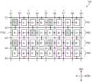
参考图1,液晶显示设备1000包括液晶面板100、定时控制器200、栅极驱动器300和数据驱动器400。Referring to FIG. 1 , a liquid
液晶面板100包括下基板110、面对下基板110的上基板120以及插入在下基板110和上基板120之间的液晶层130。The
显示面板110包括在第一方向DR1上延伸的多个栅极线G1至Gm和在与第一方向DR1交叉的第二方向DR2上延伸的多个数据线D1至Dn。栅极线G1至Gm和数据线D1至Dn定义像素区域并且像素PX被分别地置于像素区域中。图2示出连接到第一栅极线G1和第一数据线D1的像素PX。The
每个像素PX包括连接到栅极线G1至Gm中的对应栅极线的薄膜晶体管TR、连接到薄膜晶体管TR的液晶电容器Clc和并联连接到液晶电容器Clc的存储电容器Cst。必要时可以省略存储电容器Cst。薄膜晶体管TR被置于下基板110上。薄膜晶体管TR包括连接到第一栅极线G1的栅极电极、连接到第一数据线D1的源极电极以及连接到液晶电容器Clc和存储电容器Cst的漏极电极。Each pixel PX includes a thin film transistor TR connected to a corresponding one of the gate lines G1 to Gm, a liquid crystal capacitor Clc connected to the thin film transistor TR, and a storage capacitor Cst connected in parallel to the liquid crystal capacitor Clc. The storage capacitor Cst may be omitted if necessary. The thin film transistor TR is placed on the
液晶电容器Clc包括作为其两个端子的置于下基板110上的像素电极PE和置于上基板120上的公共电极CE、以及充当介电质的置于像素电极PE和公共电极CE之间的液晶层130。像素电极PE被连接到薄膜晶体管TR并且公共电极CE被置于上基板120的整个表面上以接收公共电压。与图2中示出的公共电极CE不同,根据实施例,公共电极CE可以被置于下基板110上,并且在该情况下,像素电极PE和公共电极CE中的至少一个包括隙缝。The liquid crystal capacitor Clc includes as its two terminals a pixel electrode PE placed on the
存储电容器Cst协助液晶电容器Clc,并且包括像素电极PE、存储线(未示出)以及置于像素电极PE和存储线(未示出)之间的绝缘层。存储线被置于下基板110上以与像素电极PE的一部分重叠。存储线被施加例如存储电压的恒定电压。The storage capacitor Cst assists the liquid crystal capacitor Clc, and includes a pixel electrode PE, a storage line (not shown), and an insulating layer interposed between the pixel electrode PE and the storage line (not shown). The storage line is placed on the
像素PX显示原色之一。原色包括红色、绿色、蓝色和白色色彩,但是它们不应当被限制于此或者由此被限制。原色可以进一步包括各种色彩,例如,青色、品红色、黄色,等等。像素PX可以进一步包括滤色器CF以表现原色之一。在图2中,滤色器CF被置于上基板120上,但是其不应当被限制于此或者由此被限制。也就是说,滤色器CF可以被置于下基板110上。Pixel PX displays one of the primary colors. Primary colors include red, green, blue, and white colors, but they should not be limited thereto or thereby. Primary colors may further include various colors, eg, cyan, magenta, yellow, and the like. The pixel PX may further include a color filter CF to express one of the primary colors. In FIG. 2, the color filter CF is placed on the
定时控制器200从外部图形控制器(未示出)接收图像数据RGB和控制信号。控制信号包括:作为帧区分信号的垂直同步信号Vsync;作为行区分信号的水平同步信号Hsync;为了指示数据输入时段而在其中输出数据的时段期间维持在高电平的数据使能信号DE;和主时钟信号MCLK。The
定时控制器200分析图像数据RGB,并且当确定需要调整图像数据RGB时调整图像数据RGB。当不需要对图像数据RGB进行调整时,定时控制器200不调整图像数据RGB。The
定时控制器200考虑数据驱动器400的规范来转换图像数据RGB或调整后图像数据。定时控制器200向数据驱动器400施加转换后的数据DATA。定时控制器200生成栅极控制信号GS1和数据控制信号DS1。栅极控制信号GS1被施加到栅极驱动器300,并且数据控制信号DS1被施加到数据驱动器400。The
栅极控制信号GS1用于驱动栅极驱动器300,并且数据控制信号DS1用于驱动数据驱动器400。The gate control signal GS1 is used to drive the
栅极驱动器300响应于栅极控制信号GS1而生成栅极信号并且向栅极线G1至Gm施加栅极信号。栅极控制信号GS1包括指示扫描的开始的扫描起始信号、控制栅极导通电压的输出时段的至少一个时钟信号以及控制栅极导通电压的维持的输出使能信号。The
数据驱动器400响应于数据控制信号DS1来生成与图像数据DATA相对应的灰度级电压并且将灰度级电压作为数据电压施加到数据线D1至Dn。数据电压包括相对于公共电压具有正值的正(+)数据电压和相对于公共电压具有负值的负(-)数据电压。数据控制信号DS1包括指示向数据驱动器400传送图像数据DATA的开始的水平起始信号STH、指示向数据线D1至Dn施加数据电压的加载信号以及相对于公共电压来反转数据电压的极性的极性控制信号。The
每个帧周期地将施加到像素PX的数据电压的极性反转以防止液晶被烧坏或降质。例如,数据驱动器400响应于极性控制信号来每个帧周期地反转数据电压的极性。此外,当显示与一个帧相对应的图像时,以至少一个数据线为单位输出具有不同极性的数据电压并且将其施加到像素以提高显示质量。The polarity of the data voltage applied to the pixel PX is inverted every frame period to prevent the liquid crystal from being burned out or degraded. For example, the
定时控制器200、栅极驱动器300和数据驱动器400中的每一个可以被直接地安装在液晶面板100上、在安装在柔性印刷电路板上或安装在单独的印刷电路板上之后以带载封装附接于液晶面板100。作为另一种方式,栅极驱动器300和数据驱动器400中的至少一个可以与栅极线G1至Gm、数据线D1至Dn以及薄膜晶体管TR一起被集成在液晶面板100上。另外,定时控制器200、栅极驱动器300和数据驱动器400可以被集成在单个芯片中。Each of the
图3是示出根据本公开的示例性实施例的液晶面板的一部分的平面图。FIG. 3 is a plan view illustrating a portion of a liquid crystal panel according to an exemplary embodiment of the present disclosure.
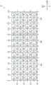
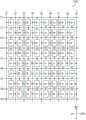
参考图3,像素包括布置在第h(h是自然数)行中的像素和布置在第h-1行中的像素。第一像素行PR1和第二像素行PR2被安置为在第二方向DR2上彼此相邻,使得栅极线G1至Gm之中的第k+1(k是自然数)栅极线被置于第一和第二像素行PR1和PR2之间。图3示出第一、第二、第三和第四像素行PR1、PR2、PR3和PR4,并且在第二方向DR2上彼此相邻的两个像素行具有相同的结构。在下文中,当假定“k”和“h”中的每一个是1时,将参考图3对第一和第二像素行PR1和PR2进行详细地描述。Referring to FIG. 3 , the pixels include pixels arranged in the h-th (h is a natural number) row and pixels arranged in the h-1-th row. The first pixel row PR1 and the second pixel row PR2 are arranged adjacent to each other in the second direction DR2 such that the k+1th (k is a natural number) gate line among the gate lines G1 to Gm is arranged at the th between the first and second pixel rows PR1 and PR2. 3 shows first, second, third and fourth pixel rows PR1, PR2, PR3 and PR4, and two pixel rows adjacent to each other in the second direction DR2 have the same structure. Hereinafter, when each of "k" and "h" is assumed to be 1, the first and second pixel rows PR1 and PR2 will be described in detail with reference to FIG. 3 .
第一像素行PR1包括在第一方向DR1中顺序地布置的第一像素组PG1和第二像素组PG2。第二像素行PR2包括在第一方向DR1中顺序地布置的第三像素组PG3和第四像素组PG4。第一至第四像素组PG1至PG4中的每一个包括偶数个像素。在图3中,第一至第四像素组PG1至PG4中的每一个包括两个像素。The first pixel row PR1 includes a first pixel group PG1 and a second pixel group PG2 sequentially arranged in the first direction DR1. The second pixel row PR2 includes a third pixel group PG3 and a fourth pixel group PG4 sequentially arranged in the first direction DR1. Each of the first to fourth pixel groups PG1 to PG4 includes an even number of pixels. In FIG. 3 , each of the first to fourth pixel groups PG1 to PG4 includes two pixels.
第一至第四像素组PG1至PG4中的每一个显示原色的一部分。第一和第四像素组PG1和PG4中的每一个包括红色像素和绿色像素。第二和第三像素组PG2和PG3中的每一个包括蓝色像素和白色像素。Each of the first to fourth pixel groups PG1 to PG4 displays a part of the primary color. Each of the first and fourth pixel groups PG1 and PG4 includes red pixels and green pixels. Each of the second and third pixel groups PG2 and PG3 includes blue pixels and white pixels.
可以重复地布置第一至第四像素组PG1至PG4。The first to fourth pixel groups PG1 to PG4 may be repeatedly arranged.
在图3中,分别通过“R”、“G”、“B”和“W”来指示红色、绿色、蓝色和白色像素。分别通过“R+”、“G+”、“B+”和“W+”来表示在第i(i是自然数)帧周期期间被施加有具有正(+)极性的数据电压的像素,并且分别通过“R-”、“G-”、“B-”和“W-”来表示在第i帧周期期间被施加有具有负(-)极性的数据电压的像素。In Figure 3, red, green, blue and white pixels are indicated by "R", "G", "B" and "W", respectively. Pixels to which a data voltage having a positive (+) polarity is applied during the i-th (i is a natural number) frame period are denoted by "R+", "G+", "B+", and "W+", respectively, and by " R-", "G-", "B-" and "W-" to represent pixels to which a data voltage having a negative (-) polarity is applied during the i-th frame period.
施加到图3中示出的液晶面板100的像素的数据电压的极性指示在第i帧周期期间数据电压的极性。在第i+1帧周期期间数据电压的极性被反转。也就是说,图1中示出的数据驱动器400每个帧周期地将施加到数据线D1至Dn的数据电压的极性反转。The polarity of the data voltage applied to the pixels of the
同时,像素的布置不应当限于图3中示出的布置。也就是说,在第一和第二像素行PR1和PR2中的每一个中,红色、绿色、蓝色和白色像素的位置可以是各种形式。详细地,第一和第二像素组PG1和PG2中的每一个可以包括绿色和白色像素。此外,第一和第四像素组PG1和PG4中的每一个可以包括红色和白色像素,并且第二和第四像素组PG2和PG3中的每一个可以包括绿色和蓝色像素。Meanwhile, the arrangement of pixels should not be limited to the arrangement shown in FIG. 3 . That is, in each of the first and second pixel rows PR1 and PR2, the positions of red, green, blue, and white pixels may be in various forms. In detail, each of the first and second pixel groups PG1 and PG2 may include green and white pixels. Also, each of the first and fourth pixel groups PG1 and PG4 may include red and white pixels, and each of the second and fourth pixel groups PG2 and PG3 may include green and blue pixels.
在本示例性实施例中,每个数据线地将施加到数据线D1至D9的数据电压的极性反转。如图3中所示,正数据电压被施加到奇数编号的数据线D1、D3、D5、D7和D9,并且负数据电压被施加到偶数编号的数据线D2、D4、D6和D8。In the present exemplary embodiment, each data line inverts the polarities of the data voltages applied to the data lines D1 to D9. As shown in FIG. 3, positive data voltages are applied to odd-numbered data lines D1, D3, D5, D7, and D9, and negative data voltages are applied to even-numbered data lines D2, D4, D6, and D8.
布置在被置于第j(j是自然数)数据线和第j+1数据线之间的第u(u是一自然数)列中的像素以至少一个像素为单位交替地连接到第j数据线和第j+1数据线。在下文中,当假定“j”和“u”中的每一个是1时,将对置于第一数据线D1和第二数据线D2之间的像素进行详细地描述。Pixels arranged in the u-th (u is a natural number) column placed between the j-th (j is a natural number) data line and the j+1-th data line are alternately connected to the j-th data line in units of at least one pixel and the j+1th data line. Hereinafter, when each of 'j' and 'u' is assumed to be 1, a pixel placed between the first data line D1 and the second data line D2 will be described in detail.
布置在第一和第二数据线D1和D2之间的第一列中的像素以至少一个像素为单位交替地连接到第一和第二数据线D1和D2。换句话说,布置在同一列中的像素以一行为单位交替地连接到左数据线和右数据线。第一像素组PG1的红色像素R+连接到第一数据线D1,并且第三像素组PG3的蓝色像素B-连接到第二数据线D2。The pixels arranged in the first column between the first and second data lines D1 and D2 are alternately connected to the first and second data lines D1 and D2 in units of at least one pixel. In other words, the pixels arranged in the same column are alternately connected to the left and right data lines in units of one row. The red pixels R+ of the first pixel group PG1 are connected to the first data line D1, and the blue pixels B- of the third pixel group PG3 are connected to the second data line D2.
在本示例性实施例中,布置在第2u-1列中的像素之中的、使得第2k栅极线被置于两个像素之间的、在第二方向DR2上彼此相邻的两个像素共同地连接到第2k栅极线。此外,布置在第2u列中的像素之中的、使得第2k-1栅极线被置于两个像素之间的、在第二方向DR2上彼此相邻的两个像素共同地连接到第2k-1栅极线。In the present exemplary embodiment, among the pixels in the 2u-1th column, two adjacent to each other in the second direction DR2 are arranged such that the 2kth gate line is placed between the two pixels The pixels are commonly connected to the 2kth gate line. Further, two pixels adjacent to each other in the second direction DR2 among the pixels arranged in the 2u-th column such that the 2k-1-th gate line is interposed between the two pixels are commonly connected to the 2k-1 gate lines.
详细地,在布置在第一列中的像素之中,彼此相邻的、使得第二栅极线G2被置于红色和蓝色像素R+和B-之间的红色和蓝色像素R+和B-共同地连接到第二栅极线G2,并且在布置在第三列中的像素之中,彼此相邻的、使得第二栅极线G2被置于红色和蓝色像素R-和B+之间的红色和蓝色像素R-和B+共同地连接到第二栅极线G2。因此,响应于施加到第二栅极线G2的栅极信号,布置在第一列中并且连接到第二栅极线G2的红色和蓝色像素R+和B-被驱动。响应于施加到第二栅极线G2的栅极信号,布置在第三列中并且连接到第二栅极线G2的红色和蓝色像素R-和B+被驱动。In detail, among the pixels arranged in the first column, the red and blue pixels R+ and B adjacent to each other such that the second gate line G2 is interposed between the red and blue pixels R+ and B- - is commonly connected to the second gate line G2 and, among the pixels arranged in the third column, are adjacent to each other such that the second gate line G2 is placed between the red and blue pixels R- and B+ The red and blue pixels R- and B+ in between are commonly connected to the second gate line G2. Therefore, in response to the gate signal applied to the second gate line G2, the red and blue pixels R+ and B- arranged in the first column and connected to the second gate line G2 are driven. In response to the gate signal applied to the second gate line G2, the red and blue pixels R- and B+ arranged in the third column and connected to the second gate line G2 are driven.
此外,在布置在第二列中的像素之中,彼此相邻的、使得第三栅极线G3被置于白色和绿色像素W+和G-之间的白色和绿色像素W+和G-共同地连接到第三栅极线G3,并且在布置在第四列中的像素之中,彼此相邻的、使得第三栅极线G3被置于白色和绿色像素W-和G+之间的白色和绿色像素W-和G+共同地连接到第三栅极线G3。因此,响应于施加到第三栅极线G3的栅极信号,布置在第二列中并且连接到第三栅极线G3的白色和绿色像素W+和G-被驱动。响应于施加到第三栅极线G3的栅极信号,布置在第四列中并且连接到第三栅极线G3的白色和绿色像素W-和G+被驱动。Further, among the pixels arranged in the second column, the white and green pixels W+ and G- adjacent to each other such that the third gate line G3 is interposed between the white and green pixels W+ and G- are commonly Connected to the third gate line G3, and among the pixels arranged in the fourth column, white and white pixels adjacent to each other such that the third gate line G3 is placed between the white and green pixels W- and G+. The green pixels W- and G+ are commonly connected to the third gate line G3. Therefore, in response to the gate signal applied to the third gate line G3, the white and green pixels W+ and G- arranged in the second column and connected to the third gate line G3 are driven. In response to the gate signal applied to the third gate line G3, the white and green pixels W- and G+ arranged in the fourth column and connected to the third gate line G3 are driven.
根据另一个实施例,布置在第2u-1列中的像素之中的、使得第2k-1栅极线被置于两个像素之间的、在第二方向DR2上彼此相邻的两个像素共同地连接到第2k-1栅极线。此外,布置在第2u列中的像素之中的、使得第2k栅极线被置于两个像素之间的、在第二方向DR2上彼此相邻的两个像素共同地连接到第2k栅极线。According to another embodiment, among the pixels in the 2u-1 column, two adjacent to each other in the second direction DR2 such that the 2k-1 gate line is placed between the two pixels The pixels are commonly connected to the 2k-1th gate line. Further, two pixels adjacent to each other in the second direction DR2 among the pixels arranged in the 2u-th column such that the 2k-th gate line is placed between the two pixels are commonly connected to the 2k-th gate polar line.
根据本示例性实施例,布置在第h行中的像素之中的显示第一色彩并且连接到第k栅极线的第一像素接收具有与施加到布置在第h+1行中的像素之中的显示第一色彩并且连接到第k栅极线的第二像素的数据电压的极性不同的极性的数据电压。第一像素和第二像素在第一方向DR1上彼此间隔开。第一像素和第二像素彼此间隔开,使得布置在奇数列中的像素被置于第一和第二像素之间。也就是说,每一个第一像素的列可以不同于每一个第二像素的列。According to the present exemplary embodiment, the first pixel that displays the first color and is connected to the k-th gate line among the pixels arranged in the h-th row receives the Data voltages of polarities different from the polarities of the data voltages of the second pixels that display the first color and are connected to the k-th gate line. The first pixel and the second pixel are spaced apart from each other in the first direction DR1. The first and second pixels are spaced apart from each other such that pixels arranged in odd-numbered columns are interposed between the first and second pixels. That is, the column of each first pixel may be different from the column of each second pixel.
第一色彩可以是红色、绿色、蓝色和白色色彩之一。The first color may be one of red, green, blue and white colors.
在第一至第四像素组PG1至PG4中,当第一像素被包括在第一像素组PG1中时,第二像素被包括在第四像素组PG4中。根据另一个实施例中,当第一像素被包括在第二像素组PG2中时,第二像素被包括在第三像素组PG3中。换句话说,当第一像素被包括在布置在第2u-1列中的像素中时,第二像素被包括在布置在第2u+1列中的像素中。此外,当第一像素被包括在布置在第2u列中的像素中时,第二像素被包括在布置在第2u-2列中的像素中。In the first to fourth pixel groups PG1 to PG4, when the first pixel is included in the first pixel group PG1, the second pixel is included in the fourth pixel group PG4. According to another embodiment, when the first pixel is included in the second pixel group PG2, the second pixel is included in the third pixel group PG3. In other words, when the first pixel is included in the pixels arranged in the 2u-1th column, the second pixel is included in the pixels arranged in the 2u+1th column. Further, when the first pixel is included in the pixels arranged in the 2u-th column, the second pixel is included in the pixels arranged in the 2u-2-th column.
当第一色彩是红色并且第一和第二像素中的每一个是红色像素时,布置在第一像素行PR1中的红色像素R+和布置在第二像素行PR2中的红色像素R-连接到第二栅极线G2,但是布置在第一像素行PR1中的红色像素R+接收具有与施加到布置在第二像素行PR2中的红色像素R-的数据电压的极性不同的极性的数据电压。When the first color is red and each of the first and second pixels is a red pixel, the red pixel R+ arranged in the first pixel row PR1 and the red pixel R- arranged in the second pixel row PR2 are connected to The second gate line G2, but the red pixels R+ arranged in the first pixel row PR1 receive data having a polarity different from that of the data voltage applied to the red pixels R- arranged in the second pixel row PR2 Voltage.
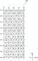
图4A是示出根据第一比较示例的液晶面板的一部分的平面图,并且图4B是示出根据第二比较示例的液晶面板的一部分的平面图。4A is a plan view showing a part of a liquid crystal panel according to a first comparative example, and FIG. 4B is a plan view showing a part of a liquid crystal panel according to a second comparative example.
在下文,将参考图4A和图4B来描述根据第一和第二比较示例的液晶面板,并且将对根据图3中示出的本示例性实施例的液晶面板100的效果进行描述。Hereinafter, the liquid crystal panels according to the first and second comparative examples will be described with reference to FIGS. 4A and 4B , and the effects of the
参考图4A和图4B,根据第一比较示例的第一比较液晶面板1A和根据第二比较示例的第二比较液晶面板1B中的每一个包括多个像素。以红色、绿色、蓝色和白色像素的次序对布置在奇数编号的行中的像素进行布置,并且以蓝色、白色、红色和绿色像素的次序对布置在偶数编号的行中的像素进行布置。Referring to FIGS. 4A and 4B , each of the first comparative
第一和第二比较液晶面板1A和1B的每一个像素连接到下栅极线和左数据线。Each pixel of the first and second comparison
以正、负、负和正极性来重复施加到第一比较液晶面板1A的数据线D1至D9的数据电压的极性。详细地,施加到第一比较液晶面板1A的数据线D1至D9的数据电压的极性分别地是+、-、-、+、+、-、-、+和+。The polarities of the data voltages applied to the data lines D1 to D9 of the first comparative
每四个数据线地将施加到第二比较液晶面板1B的数据线D1至D9的数据电压的极性反转,并且在四个数据线中每一个数据线地将数据电压的极性反转。详细地,施加到第二比较液晶面板1B的数据线D1至D9的数据电压的极性分别地是+、-、+、-、-、+、-、+和+。The polarities of the data voltages applied to the data lines D1 to D9 of the second comparison
每个帧周期地将施加到第一和第二比较液晶面板1A和1B的像素的数据电压的极性反转。The polarities of the data voltages applied to the pixels of the first and second comparison
图5是示出其中出现水平串扰的液晶面板1的视图。FIG. 5 is a view showing the
图5中示出的液晶面板1在第一区域AR1中显示例如红色的原色。The
当在一个水平扫描时段1H期间施加到显示原色的像素的数据电压的极性之和被偏压到正或负极性时,由于数据线和公共电极之间的耦合现象而不会恒定地维持公共电压。因此,在公共电压的正向或负向中出现波纹(ripple)。在该情况下,在第二和第三区域AR2和AR3中出现水平串扰,其中感觉到在外围区域AR4和在第一方向DR1上与显示原色的第一区域AR1相邻的第二及第三区域AR2及AR3之间的亮度差。When the sum of the polarities of the data voltages applied to the pixels displaying the primary colors during one horizontal scanning period 1H is biased to the positive or negative polarity, the common is not constantly maintained due to the coupling phenomenon between the data lines and the common electrodes Voltage. Therefore, ripples appear in the positive or negative direction of the common voltage. In this case, horizontal crosstalk occurs in the second and third areas AR2 and AR3, in which the second and third areas that are adjacent to the first area AR1 displaying the primary color in the peripheral area AR4 and in the first direction DR1 are felt Brightness difference between areas AR2 and AR3.
在下文,将参考图4A来描述通过正或负数据电压驱动的第一比较液晶面板1A的红色像素。参考图4A,包括在布置在第一比较液晶面板1A的第一行中的像素中的红色像素R+响应于施加到第一栅极线G1的栅极信号在第一水平扫描时段1H期间接收正数据电压。在该情况下,在公共电压的正向中出现波纹。另外,包括在布置在第一比较液晶面板1A的第二行中的像素中的红色像素R-响应于施加到第二栅极线G2的栅极信号在第一水平扫描时段1H之后的第二水平扫描时段1H期间接收负数据电压。在该情况下,在公共电压的负向中出现波纹。Hereinafter, the red pixels of the first comparative
将参考图4B来描述通过正或负数据电压驱动的第二比较液晶面板1B的红色像素。参考图4B,第二比较液晶面板1B在第i帧周期期间在第五和第六区域AR5和AR6中显示红色图像并且在第i+1帧周期期间在第六和第七区域AR6和AR7中显示红色图像。在这种情况下,被施加有正数据电压的红色像素和被施加有负数据电压的红色像素之间出现亮度差,并且结果,当第i帧周期改变为第i+1帧周期时,垂直线看起来发生移动。垂直线看起来发生移动的现象被称作移动线污点(moving line-stain)。移动线污点可能不仅仅出现在显示特定色彩的像素中而且也出现在显示白色的像素中。The red pixels of the second comparative
也就是说,在图4A中示出的第一比较液晶面板1A中出现水平串扰并且在图4B中示出的第二比较液晶面板1B中出现移动线污点。That is, horizontal crosstalk occurs in the first comparative
再次参考图3,在一个水平扫描时段期间响应于施加到第二栅极线G2的栅极信号来驱动包括在布置在液晶面板100的第一行中的像素中的红色像素R+和包括在布置在液晶面板100的第二行中的像素中的红色像素R-。Referring again to FIG. 3 , the red pixels R+ included in the pixels arranged in the first row of the
第一和第五数据线D1和D5连接到布置在第一行中的红色像素R+以向红色像素R+施加正数据电压。第四和第八数据线D4和D8连接到布置在第二行中的红色像素R-以向红色像素R-施加负数据电压。也就是说,在一个水平时段期间施加到像素以显示红色的数据电压的极性相对于彼此有偏移,并且因此在公共电压中不出现波纹。因此,可以改善水平串扰现象。The first and fifth data lines D1 and D5 are connected to the red pixels R+ arranged in the first row to apply a positive data voltage to the red pixels R+. The fourth and eighth data lines D4 and D8 are connected to the red pixels R- arranged in the second row to apply a negative data voltage to the red pixels R-. That is, the polarities of the data voltages applied to the pixels to display red during one horizontal period are shifted with respect to each other, and thus no ripple occurs in the common voltage. Therefore, the horizontal crosstalk phenomenon can be improved.
此外,因为在图3中示出的液晶面板100中布置在同一行中并且显示相同色彩的像素接收具有相同极性的数据电压,所以可以改善移动线污点现象。也就是说,可以改善水平串扰现象和移动线污点现象。In addition, since pixels arranged in the same row and displaying the same color in the
图6是示出通过图3中示出的液晶面板100所显示的图像数据的第一图案PTN1的视图。FIG. 6 is a view showing a first pattern PTN1 of image data displayed by the
参考图1和图6,图像数据RGB在液晶面板100上显示第一图案PTN1。根据第一图案PTN1,在共同地连接到一个栅极线的第一和第二像素之中,在第一像素中显示图像,但是在第二像素中不显示图像。详细地,在第一图案PTN1的第一方向DR1上延伸的边界被置于第三像素行PR3中的第一像素和第四像素行PR4中的第二像素之间。第一图案PTN1在布置在第三像素行PR3中的第一像素中显示图像并且在布置在第四像素行PR4中的第二像素中不显示图像。Referring to FIGS. 1 and 6 , the image data RGB displays the first pattern PTN1 on the
在下文中,将在第一至第三像素行PR1至PR3中显示的红色图像描述为第一图案PTN1,并且在其中不显示第一图案PTN1的第四像素行PR4中的红色像素中显示黑色图像。根据第一图案PTN1的显示,包括在第一至第三像素行PR1至PR3中的红色像素显示红色图像,但是包括在第四像素行PR4中的红色像素显示黑色图像。Hereinafter, the red image displayed in the first to third pixel rows PR1 to PR3 is described as the first pattern PTN1, and the black image is displayed in the red pixel in the fourth pixel row PR4 in which the first pattern PTN1 is not displayed . According to the display of the first pattern PTN1, the red pixels included in the first to third pixel rows PR1 to PR3 display a red image, but the red pixels included in the fourth pixel row PR4 display a black image.
在向第四栅极线G4施加栅极信号的时间期间,正(+)数据电压被施加到布置在第三像素行PR3中的红色像素R+,并且未向布置在第四像素行PR4中的红色像素R-施加电压。因此,当向第四栅极线G4施加栅极信号时,在公共电压的正向出现波纹,并且以一个线形出现水平串扰(单线串扰)。During the time when the gate signal is applied to the fourth gate line G4, the positive (+) data voltage is applied to the red pixels R+ arranged in the third pixel row PR3, and is not applied to the red pixels R+ arranged in the fourth pixel row PR4. Red pixel R-applied voltage. Therefore, when the gate signal is applied to the fourth gate line G4, ripples appear in the forward direction of the common voltage, and horizontal crosstalk (single wire crosstalk) appears in one line.
图7是示出通过调整图像数据的第一图案所获取的图像的视图。FIG. 7 is a view showing an image acquired by adjusting a first pattern of image data.
参考图1、图6和图7,当图像数据RGB具有第一图案PTN1时,液晶面板100向布置在第四像素行PR4中的红色像素R-施加非零的数据电压。基于施加到布置在第三像素行PR3中的红色像素R+的数据电压来确定施加到布置在第四像素行PR4中的红色像素R-的数据电压。1, 6 and 7, when the image data RGB has the first pattern PTN1, the
当图像数据RGB具有第一图案PTN1时,定时控制器200调整图像数据RGB,并且因此不仅向布置在第三像素行PR3中的红色像素R+、而且也向布置在第四像素行PR4中的红色像素R-施加非零的数据电压。When the image data RGB has the first pattern PTN1, the
根据本示例性实施例,当图像数据RGB具有第一图案PTN1时,可以向布置在第四像素行PR4中的红色像素R-施加非零的数据电压。因为布置在第三像素行PR3中的红色像素R+接收具有与施加到布置在第四像素行PR4中的红色像素R-的数据电压的极性相反的极性的数据电压,所以可以在向第四栅极线G4施加栅极信号的时间期间防止在公共电压中出现波纹。因而,可以防止产生单线串扰。According to the present exemplary embodiment, when the image data RGB has the first pattern PTN1, a non-zero data voltage may be applied to the red pixels R- arranged in the fourth pixel row PR4. Since the red pixel R+ arranged in the third pixel row PR3 receives the data voltage having the opposite polarity to the polarity of the data voltage applied to the red pixel R- arranged in the fourth pixel row PR4, it is possible to The time period during which the gate signal is applied by the quad gate line G4 prevents the occurrence of ripples in the common voltage. Thus, the generation of single-wire crosstalk can be prevented.
图8是示出图1中示出的定时控制器200的框图。FIG. 8 is a block diagram showing the
在下文,将参考图1和图6至图8对定时控制器200进行详细地描述。Hereinafter, the
参考图8,定时控制器200包括图案分析部分210、调整确定部分220,和数据调整部分230。8 , the
图案分析部分210分析图像数据RGB的图案。图案分析部分210分析图像数据RGB的图案在第一像素中还是在第二像素中显示图像。第一和第二像素共享一个栅极线,显示相同的色彩,并且被置于彼此不同的行中。例如,图案分析部分210分析图像数据RGB的图案是否在第一像素中显示图像并且不在第二像素中显示图像。换句话说,图案分析部分210检查在图像数据RGB的图案的第一方向DR1上延伸的边界是否被置于第一和第二像素之间。The
根据分析图像数据RGB的图案的结果,当在图像数据RGB的图案的第一方向DR1上延伸的边界不是被置于第一和第二像素之间时,图案分析部分210传送图像数据RGB而不进行调整。According to the result of analyzing the pattern of the image data RGB, when the boundary extending in the first direction DR1 of the pattern of the image data RGB is not placed between the first and second pixels, the
根据分析图像数据RGB的图案的结果,当在图像数据RGB的图案的第一方向DR1上延伸的边界被置于第一和第二像素之间时,图案分析部分210输出分析信号C1。当图像数据RGB具有图6中示出的第一图案PTN1时,在第一图案PTN1的第一方向DR1上延伸的边界被置于第三像素行PR3和第四像素行PR4之间,并且因此图案分析部分210输出分析信号C1。According to the result of analyzing the pattern of the image data RGB, when the boundary extending in the first direction DR1 of the pattern of the image data RGB is placed between the first and second pixels, the
图案分析部分210使用三乘三(three by three)掩模滤波器来分析图像数据RGB并且得到在图像数据RGB的图案的第一方向DR1上延伸的边界。详细地,图案分析部分210以与按三行乘三列布置的像素相对应的数据为单位对图像数据RGB进行扫描分析,以基于分析结果得到在图像数据RGB的图案的第一方向DR1上延伸的边界。The
调整确定部分220响应于分析信号C1来确定图像数据RGB的调整。The
图像数据RGB可以包括在第一像素的至少一部分中显示的第一像素数据和在第二像素的至少一部分中显示的第二像素数据。当图像数据RGB具有第一图案PTN1时,图像数据RGB包括在布置在第三像素行中的红色像素的至少一部分中显示的第一像素数据和在布置在第四像素行PR4中的红色像素的至少一部分中显示的第二像素数据。The image data RGB may include first pixel data displayed in at least a portion of the first pixels and second pixel data displayed in at least a portion of the second pixels. When the image data RGB has the first pattern PTN1, the image data RGB includes the first pixel data displayed in at least a part of the red pixels arranged in the third pixel row and the difference between the red pixels arranged in the fourth pixel row PR4 second pixel data displayed in at least a portion.
第一像素数据具有第一灰度值并且第二像素数据具有不同于第一灰度值的第二灰度值。当图像数据RGB具有第一图案PTN1时,第一灰度值是非零并且第二灰度值是零。The first pixel data has a first grayscale value and the second pixel data has a second grayscale value different from the first grayscale value. When the image data RGB has the first pattern PTN1, the first grayscale value is non-zero and the second grayscale value is zero.
调整确定部分220检查其中显示第一像素数据的第一像素的数量是否等于或大于参考数量。当其中显示第一像素数据的第一像素的数量等于或大于参考数量时,调整确定部分220输出用于调整数据的调整信号C2。参考数量取决于引起公共电压中的波纹的、显示第一像素数据的第一像素的数量而确定。代替使用参考数量,调整确定部分220可以检查其中显示第一像素数据的第一像素的灰度电压之和是否等于或大于参考电压以决定调整确定部分220是否输出用于调整数据的调整信号C2。第一像素的参考电压取决于引起公共电压中的波纹的、显示第一像素数据的第一像素的灰度电压之和而确定。The
根据图7,其中显示图像的第三像素行PR3的红色像素的数量是两个(2)。当参考数量是一个(1)时,调整确定部分220输出调整信号C2。换句话说,当图像数据RGB具有引起单线串扰的图案时,调整确定部分220输出调整信号C2。According to FIG. 7 , the number of red pixels of the third pixel row PR3 in which the image is displayed is two (2). When the reference number is one (1), the
当显示第一像素数据的第一像素的数量或第一像素的灰度电压之和分别地小于参考数量或参考电压时,调整确定部分220输出未调整的图像数据RGB而不改变图像数据RGB。When the number of first pixels displaying the first pixel data or the sum of the grayscale voltages of the first pixels is smaller than the reference number or the reference voltage, respectively, the
数据调整部分230响应于调整信号C2来调整图像数据RGB。The
数据调整部分230调整第一和第二像素数据以允许第一和第二像素数据具有第一和第二灰度值之间的灰度值。The
数据调整部分230调整第一像素数据以生成具有小于第一灰度值的第三灰度值的第一调整后像素数据。数据调整部分230调整第二像素数据以生成具有第四灰度值的第二调整后像素数据。第三灰度值可以等于第四灰度值。数据调整部分230输出具有第一和第二调整后像素数据的调整后图像数据RGB’。The
例如,第一灰度值可以对应于最高亮度,并且第二灰度值可以对应于最低亮度,例如,黑色。其中显示第一像素数据的第一像素以最高亮度显示红色,并且其中显示第二像素数据的第二像素显示黑色。数据调整部分230调整第一和第二像素数据以生成具有与最高亮度的一半相对应的灰度值的第一和第二调整后像素数据。其中显示第一调整后像素数据的第一像素和其中显示第二调整后像素数据的第二像素中的每一个显示与最高亮度的一半相对应的红色。For example, the first grayscale value may correspond to the highest brightness, and the second grayscale value may correspond to the lowest brightness, eg, black. The first pixel in which the first pixel data is displayed displays red at the highest brightness, and the second pixel in which the second pixel data is displayed displays black. The
第三和第四灰度值中的每一个对应于第一和第二灰度值之和的一半。因此,其中显示第一和第二像素数据的第一和第二像素的亮度可以基本上与其中显示第一和第二调整后像素数据的第一和第二像素的亮度相同。例如,在于图6中示出的布置在第三像素行PR3中的红色像素R+中显示的图像的亮度可以基本上与在于图7中示出的布置在第三像素行PR3中的红色像素R+中显示的图像的亮度和布置在第四像素行PR4中的红色像素R-中显示的图像的亮度之和相同。Each of the third and fourth grayscale values corresponds to half of the sum of the first and second grayscale values. Accordingly, the brightness of the first and second pixels in which the first and second pixel data are displayed may be substantially the same as the brightness of the first and second pixels in which the first and second adjusted pixel data are displayed. For example, the brightness of the image displayed in the red pixels R+ arranged in the third pixel row PR3 shown in FIG. 6 may be substantially the same as that of the red pixels R+ arranged in the third pixel row PR3 shown in FIG. 7 . The brightness of the image displayed in and the sum of the brightness of the image displayed in the red pixel R- arranged in the fourth pixel row PR4 are the same.
在布置在第四像素行PR4中的红色像素R-之中,在连接到第四数据线D4的红色像素R-中显示的第二像素数据是基于在布置在第三像素行PR3中的红色像素R+之中的连接到第一和第五数据线D1和D5的红色像素R+中显示的第一像素数据而生成的,但是它们不应当被限制于此或者由此被限制。也就是说,在布置在第四像素行PR4中的红色像素R-之中,在连接到第四数据线D4的红色像素R-中显示的第二像素数据是基于在布置在第三像素行PR3中的红色像素R+之中的、连接到第一和第五数据线D1和D5之一的红色像素R+中显示的第一像素数据而生成的。Among the red pixels R- arranged in the fourth pixel row PR4, the second pixel data displayed in the red pixels R- connected to the fourth data line D4 is based on the red pixels arranged in the third pixel row PR3 generated from the first pixel data displayed in the red pixel R+ connected to the first and fifth data lines D1 and D5 among the pixels R+, but they should not be limited thereto or thereby. That is, among the red pixels R- arranged in the fourth pixel row PR4, the second pixel data displayed in the red pixels R- connected to the fourth data line D4 is based on the red pixels R- arranged in the third pixel row It is generated from the first pixel data displayed in the red pixel R+ connected to one of the first and fifth data lines D1 and D5 among the red pixels R+ in PR3.
根据本示例性实施例,当在图像数据RGB的图案的第一方向DR1上延伸的边界被置于第一和第二像素之间并且显示第一像素数据的第一像素的数量或第一像素的灰度电压之和分别等于或大于参考数量或参考电压时,因为第一和第二像素共享在第一像素中显示的图像的亮度,所以可以防止出现单线串扰。According to the present exemplary embodiment, when the boundary extending in the first direction DR1 of the pattern of the image data RGB is placed between the first and second pixels and displays the number of first pixels or the first pixels of the first pixel data When the sum of the grayscale voltages of , respectively, is equal to or greater than the reference number or reference voltage, since the first and second pixels share the brightness of the image displayed in the first pixel, single-line crosstalk can be prevented.
图9是示出通过图3中示出的液晶面板所显示的图像数据的第二图案PTN2的视图,并且图10是示出通过调整图像数据的第二图案所获取的图像的视图。FIG. 9 is a view showing a second pattern PTN2 of image data displayed by the liquid crystal panel shown in FIG. 3 , and FIG. 10 is a view showing an image acquired by adjusting the second pattern of image data.
参考图6和图9,第二图案PTN2可以包括与第一图案PTN1的像素不同的像素,并且在第二图案PTN2的第一方向DR1上延伸的边界可以被置于第二像素行PR2中的第一像素和第一像素行PR1中的第二像素之间。因此,类似于第一图案PTN1,在图9中示出的第二图案PTN中可能出现单线串扰。6 and 9 , the second pattern PTN2 may include pixels different from those of the first pattern PTN1, and a boundary extending in the first direction DR1 of the second pattern PTN2 may be placed in the second pixel row PR2. between the first pixel and the second pixel in the first pixel row PR1. Therefore, similar to the first pattern PTN1, single-line crosstalk may occur in the second pattern PTN shown in FIG. 9 .
参考图1、图9和图10,当图像数据RGB具有第二图案PTN2时,液晶面板100向布置在第一像素行PR1中的第二像素、即红色像素R+施加非零的数据电压。施加到布置在第一像素行PR1中的红色像素R+的数据电压是基于施加到布置在第二像素行PR2中的红色像素R-的数据电压而确定的。1 , 9 and 10 , when the image data RGB has the second pattern PTN2 , the
当图像数据RGB具有第二图案PTN2时,定时控制器200调整图像数据RGB以不仅向布置在第二像素行PR2中的红色像素R-而且也向布置在第一像素行PR1中的红色像素R+施加非零的数据电压。通过定时控制器200执行的数据调整基本上类似于参考图8所描述的数据调整,并且因此将省略其详情。When the image data RGB has the second pattern PTN2, the
根据本示例性实施例,当图像数据RGB具有第二图案PTN2时,可以向布置在第一像素行PR1中的红色像素R+施加非零的数据电压。因为布置在第一像素行PR1中的红色像素R+接收具有与施加到布置在第二像素行PR2中的红色像素R-的数据电压的极性相反的极性的数据电压,所以可以在向第一栅极线G1施加栅极信号的时间期间防止在公共电压中出现波纹。因而,可以防止产生单线串扰。According to the present exemplary embodiment, when the image data RGB has the second pattern PTN2, a non-zero data voltage may be applied to the red pixels R+ arranged in the first pixel row PR1. Since the red pixels R+ arranged in the first pixel row PR1 receive the data voltage having the opposite polarity to the polarity of the data voltage applied to the red pixels R- arranged in the second pixel row PR2, it is possible to A time period in which a gate line G1 applies a gate signal prevents ripples in the common voltage. Thus, the generation of single-wire crosstalk can be prevented.
图11是示出根据本公开的示例性实施例的、显示装置的处理数据的方法的流程图。FIG. 11 is a flowchart illustrating a method of processing data of a display device according to an exemplary embodiment of the present disclosure.
参考图1、图3、图6和图11,提供液晶面板100(S110)。液晶面板100的配置如图3中所示,并且因此将省略其详情。Referring to FIGS. 1 , 3 , 6 and 11 , a
定时控制器200接收图像数据RGB(S120)。The
然后,定时控制器200检查在图像数据RGB的图案的第一方向DR1上延伸的边界是否被置于第一和第二像素之间(S130)。通过以与按三行乘三列布置的像素相对应的数据为单位对图像数据RGB进行扫描-分析来执行边界的位置的检查(S130)。通过边界的位置的检查(S130),最初确定具有引起单线串扰的图案的图像数据。Then, the
当确定在图像数据RGB的图案的第一方向DR1上延伸的边界没有被置于第一和第二像素之间(S130)时,向液晶面板施加与图像数据RGB相对应的数据电压(S170)。也就是说,图像数据RGB未被调整。When it is determined that the boundary extending in the first direction DR1 of the pattern of the image data RGB is not placed between the first and second pixels ( S130 ), a data voltage corresponding to the image data RGB is applied to the liquid crystal panel ( S170 ) . That is, the image data RGB are not adjusted.
当确定在图像数据RGB的图案的第一方向DR1上延伸的边界被置于第一和第二像素之间(S130)时,确定显示图案的第一或第二像素的数量是否等于或大于参考数量或者第一像素的灰度电压之和是否大于参考电压(S140)。通过检查显示图案的第一或第二像素的数量或灰度电压之和(S140),补充确定具有引起单线串扰的图案的图像数据。When it is determined that the boundary extending in the first direction DR1 of the pattern of the image data RGB is placed between the first and second pixels ( S130 ), it is determined whether the number of the first or second pixels of the display pattern is equal to or greater than the reference Whether the number or the sum of the grayscale voltages of the first pixels is greater than the reference voltage (S140). By checking the number of the first or second pixels displaying the pattern or the sum of the grayscale voltages (S140), it is supplementary to determine the image data having the pattern causing the single-line crosstalk.
当确定显示图案的第一或第二像素的数量小于参考数量或者第一像素的灰度电压之和小于参考电压(S140)时,向液晶面板施加与图像数据RGB相对应的数据电压(S170)。When it is determined that the number of the first or second pixels of the display pattern is less than the reference number or the sum of the grayscale voltages of the first pixels is less than the reference voltage ( S140 ), a data voltage corresponding to the image data RGB is applied to the liquid crystal panel ( S170 ) .
当确定显示图案的第一或第二像素的数量等于或大于参考数量或者第一像素的灰度电压之和等于或大于参考电压(S140)时,对图像数据RGB进行调整(S150)。图像数据RGB包括与第一像素相对应且具有第一灰度值的第一像素数据和与第二像素相对应且具有第二灰度值的第二像素数据。通过调整图像数据RGB来生成与第一像素相对应的具有第一和第二灰度值之间的第三灰度值的第一调整后像素数据以及与第二像素相对应的具有第一和第二灰度值之间的第四灰度值的第二调整后像素数据。When it is determined that the number of the first or second pixels of the display pattern is equal to or greater than the reference number or the sum of the grayscale voltages of the first pixels is equal to or greater than the reference voltage ( S140 ), the image data RGB is adjusted ( S150 ). The image data RGB includes first pixel data corresponding to the first pixel and having a first grayscale value and second pixel data corresponding to the second pixel and having a second grayscale value. First adjusted pixel data corresponding to the first pixel having a third grayscale value between the first and second grayscale values and corresponding to the second pixel having the first and second grayscale values are generated by adjusting the image data RGB The second adjusted pixel data for the fourth grayscale value between the second grayscale values.
然后,向液晶面板100施加与调整后图像数据相对应的数据电压(S160)。Then, a data voltage corresponding to the adjusted image data is applied to the liquid crystal panel 100 (S160).
图12至图22是示出根据本公开的各个示例性实施例的液晶面板的平面图。在图12至图22中,将主要地描述与图3中示出的液晶面板的特征不同的液晶面板的特征。12 to 22 are plan views illustrating liquid crystal panels according to various exemplary embodiments of the present disclosure. In FIGS. 12 to 22 , features of the liquid crystal panel different from those of the liquid crystal panel shown in FIG. 3 will be mainly described.
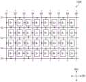
在以下实施例中,每两个数据线地将施加到数据线的数据电压的极性反转。在图12至图22中,以+、+、-、-、+、+、-和-的次序将施加到数据线的数据电压的极性反转。In the following embodiments, the polarities of the data voltages applied to the data lines are reversed every two data lines. In FIGS. 12 to 22, the polarities of the data voltages applied to the data lines are reversed in the order of +, +, -, -, +, +, -, and -.
与图3中示出的液晶面板100不同,图12至图15中示出的液晶面板100A至100D中的每一个具有布置在同一列中的像素以两个像素为单位交替地连接到与其相邻的两个数据线的结构。参考图12至图15,布置在置于第j(j是自然数)数据线和第j+1数据线之间的第u(u是自然数)列中的像素以两个像素为单位交替地连接到第j数据线和第j+1数据线。Unlike the
与图3中示出的液晶面板100不同,图13至图15中示出的液晶面板100B至100D中的每一个具有布置在同一列中的像素以两个像素为单位交替地连接到与其相邻的两个数据线的结构。参考图12至图15,布置在置于第k栅极线和第k+1栅极线之间的第h行中的像素以至少一个像素为单位交替地连接到第k栅极线和第k+1栅极线。Unlike the
参考图12,布置在置于液晶面板100A的第k栅极线和第k+1栅极线之间的第h行中的像素以一个像素为单位交替地连接到第k栅极线和第k+1栅极线。Referring to FIG. 12 , pixels arranged in the h-th row disposed between the k-th gate line and the k+1-th gate line of the
参考图13,布置在置于液晶面板100B的第k栅极线和第k+1栅极线之间的第h行中的像素以两个像素为单位交替地连接到第k栅极线和第k+1栅极线。Referring to FIG. 13 , the pixels arranged in the h-th row disposed between the k-th gate line and the k+1-th gate line of the
参考图14,布置在置于液晶面板100C的第k栅极线和第k+1栅极线之间的第h行中的像素以四个像素为单位交替地连接到第k栅极线和第k+1栅极线。Referring to FIG. 14 , pixels arranged in the h-th row disposed between the k-th gate line and the k+1-th gate line of the
参考图15,布置在置于液晶面板100D的第k栅极线和第k+1栅极线之间的第h行中的像素交替地连接到第k栅极线和第k+1栅极线,并且,布置在置于液晶面板100D的第k栅极线和第k+1栅极线之间的第h行中的像素中的每一个所连接到的栅极线以四个像素为单位改变为第k或第k+1栅极线。Referring to FIG. 15 , the pixels arranged in the h-th row disposed between the k-th gate line and the k+1-th gate line of the
除了布置在同一列中的像素以四个像素为单位交替地连接到与其相邻的两个数据线之外,图16至图19中示出的液晶面板100E至100H中的每一个具有与图12至图15中示出的液晶面板100A至100D相同的结构和功能。Each of the
除了布置在同一列中的像素以一个像素为单位交替地连接到与其相邻的两个数据线之外,图20至图22中示出的液晶面板100I至100K中的每一个具有与图13至图15中示出的液晶面板100B至100D相同的结构和功能。13 The structures and functions are the same as those of the
图12至图22中示出的液晶面板100A至100K中的每一个可以改善水平串扰现象和移动线污点现象。Each of the
尽管已经描述了本发明构思的示例性实施例,但应当理解,本发明构思不应当限于这些示例性实施例,而是在如在下文所请求保护的本发明构思的精神和范围内能够由本领域普通技术人员进行各种改变和修改。While exemplary embodiments of the present inventive concept have been described, it should be understood that the present inventive concept should not be limited to these exemplary embodiments, but rather can be implemented by those skilled in the art within the spirit and scope of the present inventive concept as hereinafter claimed. Various changes and modifications will be made by those of ordinary skill.
Claims (20)
Applications Claiming Priority (2)
| Application Number | Priority Date | Filing Date | Title |
|---|---|---|---|
| KR1020140194159AKR20160083325A (en) | 2014-12-30 | 2014-12-30 | Display apparatus and method of processing data thereof |
| KR10-2014-0194159 | 2014-12-30 |
Publications (2)
| Publication Number | Publication Date |
|---|---|
| CN105741799A CN105741799A (en) | 2016-07-06 |
| CN105741799Btrue CN105741799B (en) | 2020-03-10 |
Family
ID=54850528
Family Applications (1)
| Application Number | Title | Priority Date | Filing Date |
|---|---|---|---|
| CN201510983233.2AExpired - Fee RelatedCN105741799B (en) | 2014-12-30 | 2015-12-24 | Display device and method for processing data thereof |
Country Status (4)
| Country | Link |
|---|---|
| US (1) | US10140935B2 (en) |
| EP (1) | EP3040979A1 (en) |
| KR (1) | KR20160083325A (en) |
| CN (1) | CN105741799B (en) |
Families Citing this family (19)
| Publication number | Priority date | Publication date | Assignee | Title |
|---|---|---|---|---|
| KR20160029892A (en) | 2014-09-05 | 2016-03-16 | 삼성디스플레이 주식회사 | Display apparatus and method of driving the same |
| KR102342685B1 (en) | 2015-03-05 | 2021-12-24 | 삼성디스플레이 주식회사 | Display panel and display apparatus having the same |
| EP3288019A4 (en)* | 2015-04-24 | 2018-02-28 | Sharp Kabushiki Kaisha | Display control device, liquid crystal display device, display control program, and recording medium |
| CN106057154B (en)* | 2016-07-25 | 2018-05-25 | 京东方科技集团股份有限公司 | Pixel circuit, display device, display device and driving method |
| KR102560941B1 (en)* | 2016-09-29 | 2023-07-27 | 엘지디스플레이 주식회사 | Liquid Crystal Display Device and Liquid Crystal Display Panel |
| KR102280009B1 (en) | 2017-05-24 | 2021-07-21 | 삼성전자주식회사 | Display panel having zig-zag connection structure and display device including the same |
| JP7021407B2 (en)* | 2017-07-11 | 2022-02-17 | トライベイル テクノロジーズ, エルエルシー | Display device and its driving method |
| CN107871485B (en)* | 2017-12-19 | 2019-08-27 | 惠科股份有限公司 | Display panel, display device and driving method |
| CN107978288B (en)* | 2017-12-19 | 2020-04-07 | 惠科股份有限公司 | Display panel, display device and driving method |
| CN108761938B (en)* | 2018-05-22 | 2021-02-09 | 京东方科技集团股份有限公司 | Pixel arrangement structure, driving method thereof, display panel and display device |
| KR102532775B1 (en) | 2018-10-10 | 2023-05-17 | 삼성디스플레이 주식회사 | Display device |
| US11138944B2 (en)* | 2018-12-06 | 2021-10-05 | Xianyang Caihong Optoelectronics Technology Co., Ltd | Pixel matrix driving device and display device |
| CN111489712B (en)* | 2019-01-29 | 2022-03-11 | 咸阳彩虹光电科技有限公司 | Pixel matrix driving device and display |
| CN111292692B (en)* | 2018-12-06 | 2022-07-29 | 咸阳彩虹光电科技有限公司 | Pixel matrix driving device, pixel matrix driving method and display thereof |
| KR102659615B1 (en)* | 2019-02-28 | 2024-04-23 | 삼성디스플레이 주식회사 | Display device and driving method thereof |
| CN110462724B (en)* | 2019-06-28 | 2021-03-19 | 京东方科技集团股份有限公司 | Method for displaying image in display device, data signal compensation device for compensating data signal of display device, and display device |
| US10777155B1 (en)* | 2019-07-16 | 2020-09-15 | Himax Technologies Limited | Method for controlling polarity of each subpixels of display panel by using pattern detection manner |
| KR102716843B1 (en)* | 2019-11-12 | 2024-10-16 | 삼성디스플레이 주식회사 | Display device |
| CN118938552A (en)* | 2024-06-11 | 2024-11-12 | 南京观海微电子有限公司 | Liquid crystal display array |
Family Cites Families (22)
| Publication number | Priority date | Publication date | Assignee | Title |
|---|---|---|---|---|
| US5300942A (en) | 1987-12-31 | 1994-04-05 | Projectavision Incorporated | High efficiency light valve projection system with decreased perception of spaces between pixels and/or hines |
| JP3365357B2 (en) | 1999-07-21 | 2003-01-08 | 日本電気株式会社 | Active matrix type liquid crystal display |
| KR100825105B1 (en)* | 2002-05-04 | 2008-04-25 | 삼성전자주식회사 | Liquid crystal display |
| KR100878280B1 (en)* | 2002-11-20 | 2009-01-13 | 삼성전자주식회사 | 4-color driving liquid crystal display and display panel for use |
| KR100951350B1 (en)* | 2003-04-17 | 2010-04-08 | 삼성전자주식회사 | Liquid crystal display |
| US7397455B2 (en)* | 2003-06-06 | 2008-07-08 | Samsung Electronics Co., Ltd. | Liquid crystal display backplane layouts and addressing for non-standard subpixel arrangements |
| US7525526B2 (en) | 2003-10-28 | 2009-04-28 | Samsung Electronics Co., Ltd. | System and method for performing image reconstruction and subpixel rendering to effect scaling for multi-mode display |
| KR101243811B1 (en)* | 2006-06-30 | 2013-03-18 | 엘지디스플레이 주식회사 | A liquid crystal display device and a method for driving the same |
| KR101430149B1 (en) | 2007-05-11 | 2014-08-18 | 삼성디스플레이 주식회사 | Liquid crystal display and method of driving the same |
| CN101290444B (en)* | 2008-06-06 | 2010-07-28 | 友达光电股份有限公司 | Method for driving liquid crystal display device |
| TWI397894B (en)* | 2008-07-18 | 2013-06-01 | Novatek Microelectronics Corp | Electronic device for enhancing voltage driving efficiency for a source driver and lcd monitor thereof |
| KR101363204B1 (en)* | 2008-12-26 | 2014-02-24 | 엘지디스플레이 주식회사 | Liquid crystal display and driving method thereof |
| KR101634744B1 (en) | 2009-12-30 | 2016-07-11 | 삼성디스플레이 주식회사 | Display apparatus |
| KR101329505B1 (en)* | 2010-05-28 | 2013-11-13 | 엘지디스플레이 주식회사 | Liquid crystal display and method of driving the same |
| CN102930809B (en) | 2011-08-12 | 2016-02-10 | 上海中航光电子有限公司 | The transversely arranged dot structure that bigrid drives and display panel |
| JP5429336B2 (en)* | 2011-09-16 | 2014-02-26 | 株式会社リコー | Image processing apparatus, image processing method, and program |
| KR20130134814A (en)* | 2012-05-31 | 2013-12-10 | 삼성디스플레이 주식회사 | Liquid crystal display device |
| KR101441395B1 (en) | 2012-07-05 | 2014-09-17 | 엘지디스플레이 주식회사 | Liquid crystal display device and driving method the same |
| KR102004845B1 (en)* | 2012-12-28 | 2019-07-29 | 엘지디스플레이 주식회사 | Method of controlling polarity of data voltage and liquid crystal display using the same |
| TWI524125B (en)* | 2014-04-16 | 2016-03-01 | 友達光電股份有限公司 | Pixel array |
| KR20150139132A (en) | 2014-06-02 | 2015-12-11 | 삼성디스플레이 주식회사 | Display apparatus and method of driving the same |
| CN104155821B (en)* | 2014-08-20 | 2018-02-02 | 上海中航光电子有限公司 | TFT array substrate and driving method thereof, display panel and display device |
- 2014
- 2014-12-30KRKR1020140194159Apatent/KR20160083325A/ennot_activeCeased
- 2015
- 2015-08-28USUS14/839,653patent/US10140935B2/enactiveActive
- 2015-12-21EPEP15201643.2Apatent/EP3040979A1/ennot_activeWithdrawn
- 2015-12-24CNCN201510983233.2Apatent/CN105741799B/ennot_activeExpired - Fee Related
Also Published As
| Publication number | Publication date |
|---|---|
| EP3040979A1 (en) | 2016-07-06 |
| US20160189641A1 (en) | 2016-06-30 |
| US10140935B2 (en) | 2018-11-27 |
| CN105741799A (en) | 2016-07-06 |
| KR20160083325A (en) | 2016-07-12 |
Similar Documents
| Publication | Publication Date | Title |
|---|---|---|
| CN105741799B (en) | Display device and method for processing data thereof | |
| KR102296435B1 (en) | Display apparatus and driving method thereof | |
| CN105139813B (en) | Display device and method for driving the same | |
| US9835908B2 (en) | Display apparatus | |
| CN105405416B (en) | Display device and method of driving the same | |
| KR102306598B1 (en) | Display apparatus | |
| KR102255745B1 (en) | Display apparatus | |
| CN105549283B (en) | Display device | |
| CN105321448A (en) | Display apparatus and method of driving the same | |
| US20100265272A1 (en) | Method of processing data, data processing device for performing the method and display apparatus including the data processing device | |
| US9905187B2 (en) | Method of driving display panel and display apparatus for performing the same | |
| US20160104448A1 (en) | Display apparatus | |
| US10217424B2 (en) | Liquid crystal display utilizing a timing controller for changing polarity arrangement and method of driving the same | |
| US20110085098A1 (en) | Array substrate and flat display device | |
| CN106257579B (en) | Display device | |
| KR20190033694A (en) | Driving circuit with filtering function and display device having them | |
| US12288504B2 (en) | Electrical apparatus and driver apparatus for improving streaking of displayed image | |
| US10354604B2 (en) | Display apparatus and method of driving the same | |
| KR20170088011A (en) | Display apparatus | |
| KR20130109814A (en) | Liquid crystal display and driving method thereof | |
| US10490146B2 (en) | Display device and image processing method |
Legal Events
| Date | Code | Title | Description |
|---|---|---|---|
| C06 | Publication | ||
| PB01 | Publication | ||
| SE01 | Entry into force of request for substantive examination | ||
| SE01 | Entry into force of request for substantive examination | ||
| GR01 | Patent grant | ||
| GR01 | Patent grant | ||
| CF01 | Termination of patent right due to non-payment of annual fee | Granted publication date:20200310 Termination date:20201224 | |
| CF01 | Termination of patent right due to non-payment of annual fee |