CN1057147A - Side by side television pictures - Google Patents
Side by side television picturesDownload PDFInfo
- Publication number
- CN1057147A CN1057147ACN91103726ACN91103726ACN1057147ACN 1057147 ACN1057147 ACN 1057147ACN 91103726 ACN91103726 ACN 91103726ACN 91103726 ACN91103726 ACN 91103726ACN 1057147 ACN1057147 ACN 1057147A
- Authority
- CN
- China
- Prior art keywords
- picture
- signal
- video
- mentioned
- display
- Prior art date
- Legal status (The legal status is an assumption and is not a legal conclusion. Google has not performed a legal analysis and makes no representation as to the accuracy of the status listed.)
- Granted
Links
Images


Classifications
- H—ELECTRICITY
- H04—ELECTRIC COMMUNICATION TECHNIQUE
- H04N—PICTORIAL COMMUNICATION, e.g. TELEVISION
- H04N9/00—Details of colour television systems
- H04N9/64—Circuits for processing colour signals
- H04N9/641—Multi-purpose receivers, e.g. for auxiliary information
- G—PHYSICS
- G06—COMPUTING OR CALCULATING; COUNTING
- G06T—IMAGE DATA PROCESSING OR GENERATION, IN GENERAL
- G06T3/00—Geometric image transformations in the plane of the image
- G06T3/04—Context-preserving transformations, e.g. by using an importance map
- G—PHYSICS
- G06—COMPUTING OR CALCULATING; COUNTING
- G06T—IMAGE DATA PROCESSING OR GENERATION, IN GENERAL
- G06T3/00—Geometric image transformations in the plane of the image
- G06T3/40—Scaling of whole images or parts thereof, e.g. expanding or contracting
- G06T3/4007—Scaling of whole images or parts thereof, e.g. expanding or contracting based on interpolation, e.g. bilinear interpolation
- H—ELECTRICITY
- H04—ELECTRIC COMMUNICATION TECHNIQUE
- H04N—PICTORIAL COMMUNICATION, e.g. TELEVISION
- H04N19/00—Methods or arrangements for coding, decoding, compressing or decompressing digital video signals
- H04N19/90—Methods or arrangements for coding, decoding, compressing or decompressing digital video signals using coding techniques not provided for in groups H04N19/10-H04N19/85, e.g. fractals
- H—ELECTRICITY
- H04—ELECTRIC COMMUNICATION TECHNIQUE
- H04N—PICTORIAL COMMUNICATION, e.g. TELEVISION
- H04N3/00—Scanning details of television systems; Combination thereof with generation of supply voltages
- H04N3/10—Scanning details of television systems; Combination thereof with generation of supply voltages by means not exclusively optical-mechanical
- H04N3/16—Scanning details of television systems; Combination thereof with generation of supply voltages by means not exclusively optical-mechanical by deflecting electron beam in cathode-ray tube, e.g. scanning corrections
- H04N3/22—Circuits for controlling dimensions, shape or centering of picture on screen
- H04N3/223—Controlling dimensions
- H—ELECTRICITY
- H04—ELECTRIC COMMUNICATION TECHNIQUE
- H04N—PICTORIAL COMMUNICATION, e.g. TELEVISION
- H04N3/00—Scanning details of television systems; Combination thereof with generation of supply voltages
- H04N3/10—Scanning details of television systems; Combination thereof with generation of supply voltages by means not exclusively optical-mechanical
- H04N3/16—Scanning details of television systems; Combination thereof with generation of supply voltages by means not exclusively optical-mechanical by deflecting electron beam in cathode-ray tube, e.g. scanning corrections
- H04N3/22—Circuits for controlling dimensions, shape or centering of picture on screen
- H04N3/227—Centering
- H—ELECTRICITY
- H04—ELECTRIC COMMUNICATION TECHNIQUE
- H04N—PICTORIAL COMMUNICATION, e.g. TELEVISION
- H04N3/00—Scanning details of television systems; Combination thereof with generation of supply voltages
- H04N3/10—Scanning details of television systems; Combination thereof with generation of supply voltages by means not exclusively optical-mechanical
- H04N3/16—Scanning details of television systems; Combination thereof with generation of supply voltages by means not exclusively optical-mechanical by deflecting electron beam in cathode-ray tube, e.g. scanning corrections
- H04N3/27—Circuits special to multi-standard receivers
- H—ELECTRICITY
- H04—ELECTRIC COMMUNICATION TECHNIQUE
- H04N—PICTORIAL COMMUNICATION, e.g. TELEVISION
- H04N5/00—Details of television systems
- H04N5/222—Studio circuitry; Studio devices; Studio equipment
- H04N5/262—Studio circuits, e.g. for mixing, switching-over, change of character of image, other special effects ; Cameras specially adapted for the electronic generation of special effects
- H04N5/2624—Studio circuits, e.g. for mixing, switching-over, change of character of image, other special effects ; Cameras specially adapted for the electronic generation of special effects for obtaining an image which is composed of whole input images, e.g. splitscreen
- H—ELECTRICITY
- H04—ELECTRIC COMMUNICATION TECHNIQUE
- H04N—PICTORIAL COMMUNICATION, e.g. TELEVISION
- H04N5/00—Details of television systems
- H04N5/44—Receiver circuitry for the reception of television signals according to analogue transmission standards
- H04N5/445—Receiver circuitry for the reception of television signals according to analogue transmission standards for displaying additional information
- H04N5/45—Picture in picture, e.g. displaying simultaneously another television channel in a region of the screen
- H—ELECTRICITY
- H04—ELECTRIC COMMUNICATION TECHNIQUE
- H04N—PICTORIAL COMMUNICATION, e.g. TELEVISION
- H04N7/00—Television systems
- H04N7/007—Systems with supplementary picture signal insertion during a portion of the active part of a television signal, e.g. during top and bottom lines in a HDTV letter-box system
- H—ELECTRICITY
- H04—ELECTRIC COMMUNICATION TECHNIQUE
- H04N—PICTORIAL COMMUNICATION, e.g. TELEVISION
- H04N7/00—Television systems
- H04N7/01—Conversion of standards, e.g. involving analogue television standards or digital television standards processed at pixel level
- H—ELECTRICITY
- H04—ELECTRIC COMMUNICATION TECHNIQUE
- H04N—PICTORIAL COMMUNICATION, e.g. TELEVISION
- H04N7/00—Television systems
- H04N7/01—Conversion of standards, e.g. involving analogue television standards or digital television standards processed at pixel level
- H04N7/0105—Conversion of standards, e.g. involving analogue television standards or digital television standards processed at pixel level using a storage device with different write and read speed
- H—ELECTRICITY
- H04—ELECTRIC COMMUNICATION TECHNIQUE
- H04N—PICTORIAL COMMUNICATION, e.g. TELEVISION
- H04N7/00—Television systems
- H04N7/01—Conversion of standards, e.g. involving analogue television standards or digital television standards processed at pixel level
- H04N7/0117—Conversion of standards, e.g. involving analogue television standards or digital television standards processed at pixel level involving conversion of the spatial resolution of the incoming video signal
- H04N7/0122—Conversion of standards, e.g. involving analogue television standards or digital television standards processed at pixel level involving conversion of the spatial resolution of the incoming video signal the input and the output signals having different aspect ratios
- H—ELECTRICITY
- H04—ELECTRIC COMMUNICATION TECHNIQUE
- H04N—PICTORIAL COMMUNICATION, e.g. TELEVISION
- H04N7/00—Television systems
- H04N7/015—High-definition television systems
- H—ELECTRICITY
- H04—ELECTRIC COMMUNICATION TECHNIQUE
- H04N—PICTORIAL COMMUNICATION, e.g. TELEVISION
- H04N9/00—Details of colour television systems
- H04N9/64—Circuits for processing colour signals
Landscapes
- Engineering & Computer Science (AREA)
- Multimedia (AREA)
- Signal Processing (AREA)
- Theoretical Computer Science (AREA)
- Physics & Mathematics (AREA)
- General Physics & Mathematics (AREA)
- Computer Graphics (AREA)
- Controls And Circuits For Display Device (AREA)
- Television Systems (AREA)
- Studio Circuits (AREA)
- Details Of Television Scanning (AREA)
- Transforming Electric Information Into Light Information (AREA)
- Synchronizing For Television (AREA)
- Color Television Systems (AREA)
- Stereophonic System (AREA)
- Image Processing (AREA)
- Pinball Game Machines (AREA)
- Application Of Or Painting With Fluid Materials (AREA)
- Sealing Material Composition (AREA)
- Paints Or Removers (AREA)
- Acyclic And Carbocyclic Compounds In Medicinal Compositions (AREA)
- Organic Low-Molecular-Weight Compounds And Preparation Thereof (AREA)
- Image Analysis (AREA)
- Display Devices Of Pinball Game Machines (AREA)
- Signal Processing For Digital Recording And Reproducing (AREA)
- Compositions Of Macromolecular Compounds (AREA)
- Manipulator (AREA)
- Television Signal Processing For Recording (AREA)
- Inks, Pencil-Leads, Or Crayons (AREA)
- Liquid Crystal Display Device Control (AREA)
- Control Of Indicators Other Than Cathode Ray Tubes (AREA)
- Testing, Inspecting, Measuring Of Stereoscopic Televisions And Televisions (AREA)
- Two-Way Televisions, Distribution Of Moving Picture Or The Like (AREA)
Abstract
Translated fromChineseDescription
Translated fromChinese本发明涉及能够并列显示不同来源且幅面大致相等的多个画面的电视技术领域,特别涉及宽屏幕显示格式比宽的这种电视机。现在的大部分电视机的显示格式比(即水平宽度/垂直高度)为4∶3。有一种宽显示格式比更接近电影的显示格式比例如16∶9。本发明既可用于直观式电视机,也可用于投影电视。The invention relates to the technical field of televisions capable of displaying a plurality of pictures from different sources in parallel and with roughly equal widths, in particular to such televisions with a wide-screen display format ratio. Most televisions today have a display format ratio (ie horizontal width/vertical height) of 4:3. There is a wide display format ratio that is closer to that of a movie such as 16:9. The present invention can be used not only for direct-view TV, but also for projection TV.
显示格式比为4∶3(常称为4×3)的电视机在显示单个和多个视频信号源的方面受到限制。商业广播电台传输的电视信号(除实验性资料外)都用4×3显示格式比播出。许多观众都感到4×3显示格式不如电影所伴随的较宽的显示格式悦目。宽显示格式比的电视机不仅显示效果更为悦目,而且能够按相应的宽显示格式来显示宽显示格式的信号源。多个影片“看起来”就象电影,而不是其被限幅或畸变的型态。当视频源例如用电视电影机或者用电视机中的处理器将影片变换成视频时,都不需限幅。Televisions with a display format ratio of 4:3 (often called 4x3) are limited in their ability to display single and multiple video sources. Television signals transmitted by commercial radio stations (except for experimental material) are broadcast in a 4×3 display format. Many viewers find the 4x3 display format less pleasing than the wider display formats that accompany movies. TVs with wide display format ratios not only display more pleasing effects, but are also capable of displaying wide display format signal sources in corresponding wide display formats. Multiple movies "look" like movies, rather than clipped or distorted versions of them. Clipping is not necessary when the video source is converted from film to video, for example by a telecine or by a processor in a television.
宽显示格式比的电视机还适用于各式各样的显示,既适用于常规的也适用于宽显示格式的信号,而且还适用于这两种显示格式在多画面显示形式下的组合显示。但使用宽显示比屏幕带来许多问题。要变换多信号源的显示格式比,要从非同步但同时显示的信号源产生出一致的定时信号,要在多个信号源之间进行切换以产生多画面的显示,还要从压缩的数据信号提供高清晰度的画面,这些都是一般性的问题。本发明的宽屏幕电视能解决这些问题。按照本发明各种方案设计的宽屏幕电视机能从相同或不同显示格式比的单个和多个源提供高清晰度的单个和多个画面的显示,而且显示格式比可加以选择。Wide display format ratio televisions are also suitable for a wide variety of displays, both for conventional and wide display format signals, and for combinations of these two display formats in multi-screen display formats. But using wide aspect ratio screens brings many problems. To change the display format ratio of multiple signal sources, to generate a consistent timing signal from asynchronous but simultaneously displayed signal sources, to switch between multiple signal sources to produce multi-screen display, and to generate a consistent timing signal from compressed data The signal provides a high-definition picture, and these are general issues. The wide screen television of the present invention can solve these problems. Widescreen televisions designed in accordance with the various aspects of the invention are capable of providing high definition single and multiple picture displays from single and multiple sources of the same or different display format ratios, and the display format ratios can be selected.
宽显示格式比的电视可在采取基本或标准水平扫描速率及其倍数、并以隔行扫描和非隔行扫描的方式显示视频信号的电视系统中加以实现。例如,标准的NTSC视频信号就是通过隔行扫描各视频帧的连续场进行显示的,各场则由大约15,734Hz的基本或标准水平扫描速率的光栅扫描操作产生的。视频信号的基本扫描速率有各种各样的叫法:fH、1fH和1H。1fH信号的实际频率随不同的视频标准而异。为努力改善电视设备的画面质量,业已研制出以非隔行扫描方式逐行显示视频信号的电视系统。逐行扫描要求在为扫描隔行扫描格式两场中的一场而分配的同一时间段内扫描各显示帧。没有闪烁的AA-BB显示要求各场接连地扫描两次。在各次情况下,水平扫描频率必须是标准水平频率的2倍。这种逐行扫描或无闪烁显示的扫描速率有各种不同的叫法:2fH和2H。2fH的扫描频率例如按美国标准约为31,468Hz。Television with wide display format ratios can be implemented in television systems that display video signals in both interlaced and non-interlaced formats at the basic or standard horizontal scan rate and multiples thereof. For example, standard NTSC video signals are displayed by interlacing successive fields of video frames, each field being generated by a raster scan operation at a basic or standard horizontal scan rate of about 15,734 Hz. There are various names for the basic scan rate of a video signal: fH , 1fH , and 1H. The actual frequency of the 1fH signal varies with different video standards. In an effort to improve the picture quality of television equipment, television systems have been developed which display video signals progressively in a non-interlaced manner. Progressive scanning requires that each display frame be scanned within the same time period allotted for scanning one of the two fields in an interlaced format. An AA-BB display without flickering requires each field to be scanned twice in succession. In each case, the horizontal scanning frequency must be twice the standard horizontal frequency. This scan rate for progressive or flicker-free displays has various names: 2fH and 2H. The scanning frequency of 2fH is, for example, approximately 31,468 Hz according to US standards.
常规的显示格式比的电视设备可配备成能显示多个画面,例如来自两个视频源的画面。视频源可以是电视机中的调谐器、盒式录像机中的调谐器、摄像机等等。在通常叫做画中画(PIP)的方式下,电视机的调谐器提供充满大部分屏幕或显示区的画面,同时有一个辅助视频源提供通常在大画面的边界内的小插图。图1(C)示出了宽屏幕电视机的PIP显示方式。在许多情况下,可将插图在很多不同的位置上定位。另一种显示方式通常叫做频道扫描显示方式,这种显示方式是把各个来自不同频道源的许多小画面以停帧剪辑(freeze frame montage)的形式布满屏幕。至少就画幅来说,没有主画面。图1(i)示出了宽屏幕电视设备的频道扫描显示方式。在宽屏幕电视设备中还可以采取其他的显示方式,有一种显示方式叫做画外画(POP)显示方式。在这种显示方式下,好几个辅助插图可与主画面一起分享共同的边界范围。图1(f)示出了宽屏幕电视设备的POP显示方式。特别适用于宽屏幕电视的另一种方式是来自不同视频源(例如来自两个不同频道的)的、幅面基本相同的并列画面。在图1(d)中列举出两个4∶3视频源的宽屏幕电视来说明这种方式。可以理解为这种方式可以看作为POP方式的特殊情形。Conventional display format ratio television equipment may be equipped to display multiple frames, for example frames from two video sources. The video source could be a tuner in a TV, a tuner in a VCR, a video camera, and so on. In what is often called picture-in-picture (PIP), the TV's tuner provides a picture that fills most of the screen or display area, while a secondary video source provides a vignette, usually within the boundaries of the larger picture. Figure 1(C) shows the PIP display method of a wide-screen TV. In many cases, the artwork can be positioned in many different positions. Another display method is usually called a channel scan display method. This display method is to fill the screen with many small pictures from different channel sources in the form of freeze frame montage. At least as far as the format is concerned, there is no main picture. Fig. 1(i) shows a channel scanning display mode of a wide-screen TV device. Other display methods can also be adopted in wide-screen TV equipment, and there is a display method called Picture-Outside-Picture (POP) display method. In this display, several secondary illustrations can share a common border with the main image. Figure 1(f) shows the POP display mode of wide-screen TV equipment. Another approach, particularly suitable for widescreen television, is side-by-side pictures of substantially the same size from different video sources (eg, from two different channels). In Figure 1(d), two wide-screen TVs with 4:3 video sources are listed to illustrate this approach. It can be understood that this method can be regarded as a special case of the POP method.
宽屏电视机水平扫描的持续时间与常规的电视机的一样。但宽屏电视机中水平扫描的行程更长。这会使画面在水平方向上拉长,在显示出的画面中产生影象宽高比显著的畸变。因此在诸如显示格式比为16∶9的宽屏幕电视机上显示常规的4∶3显示格式比的视频信号时就会有问题。这些特定的显示格式比可能导致水平拉长或扩展为4/3倍。这是将显示格式比为4∶3的画面作为主画面和辅助画面(例如以PIP或POP的形式显示)时的一个问题。对于PIP和POP方式而言,即使在主画面来自显示格式比为16∶9的视频源、并与电视机的显示装置相匹配的情况下也会有这个问题。The duration of the horizontal scan of a widescreen TV is the same as that of a conventional TV. But the horizontal scan travel is longer in widescreen TVs. This stretches the picture horizontally, producing significant aspect ratio distortion in the displayed picture. Problems can therefore arise when displaying a conventional 4:3 display format ratio video signal on, for example, a wide screen television set having a display format ratio of 16:9. These specific display format ratios may result in horizontal stretching or expansion by a factor of 4/3. This is a problem when using a picture with a display format ratio of 4:3 as the main picture and the auxiliary picture (for example, displayed in the form of PIP or POP). For the PIP and POP modes, this problem occurs even when the main picture is from a video source with a display format ratio of 16:9 and matches the display device of the television set.
现在可以购得某些数字电路通常叫做画中画处理器,它在常规的电视机中实现PIP和频道扫描显示方式。这类画中画处理器有一种叫做CPIP芯片,可从美国印第安纳洲的印第安纳波利斯市汤姆逊消费者电子设备公司(Thomson Consumer Electronics Inc)购得。该公司出的《CTC140画中画(CPIP)技术培训手册》中全面地介绍了CPIP芯片。这种画中画处理器不适宜在宽屏幕电视机中实现特殊显示方式,例如PIP、POP和频道扫描显示方式。如果在宽屏幕电视机中没有外部加速电路而显示这种由画中画处理器从辅助视频源处理出来的辅助画面,单个或多个辅助画面会产生上述的几何畸变。由于较宽画面的显像管的较宽的水平扫描动作无论是直观电视或者投影电视显示出来的辅助画面都会在水平方向上按4/3扩展。如果采用外加速电路,则显示出来的辅助画面不会产生宽高比畸变,但可能不会充满整个屏幕或屏幕上在其它情况下可能分派给辅助显示的部分。Certain digital circuits are now commercially available, commonly called picture-in-picture processors, which implement the PIP and channel scan display modes in conventional televisions. One such picture-in-picture processor is a chip called a CPIP, available from Thomson Consumer Electronics Inc of Indianapolis, Indiana, USA. The company's "CTC140 Picture-in-Picture (CPIP) Technical Training Manual" fully introduces the CPIP chip. This picture-in-picture processor is not suitable for realizing special display modes in wide-screen TV sets, such as PIP, POP and channel scanning display modes. If such an auxiliary picture processed by a picture-in-picture processor from an auxiliary video source is displayed in a widescreen television set without an external acceleration circuit, single or multiple auxiliary pictures will produce the above-mentioned geometric distortion. Due to the wider horizontal scanning action of the picture tube of the wider picture, no matter the auxiliary picture displayed by direct-view TV or projection TV will expand by 4/3 in the horizontal direction. If an external accelerator circuit is used, the auxiliary picture is displayed without aspect ratio distortion, but may not fill the entire screen or the portion of the screen that might otherwise be allocated to the auxiliary display.
宽屏幕电视机可配备一个使视频信号(例如辅助视频信号)失真的信号处理器,以使后来显示的辅助画面不会产生图象宽高比畸变。那种畸变可用不对称压缩的方法获得的。压缩因数取决于辅助视频信号和宽屏幕电视机的相对显示格式比而定。为在显示格式比为16∶9的电视机上显示出显示格式比为4∶3的辅助视频信号,要将辅助画面在水平方向上按4∶1压缩,在垂直方向上按3∶1压缩。在显示格式比不同(例如为2∶1)的电视机中,水平压缩因数会比垂直压缩因数大1.5倍。不对称压缩产生几何畸变的画面,然后将其存储在与画中画处理器相关联的视频存储器中。按画中画处理器的正常操作方式从存储器中读出经不对称压缩的辅助画面时,无论显示方式采取PIP、POP、频道扫描或其它显示方式,由此得出的辅助显示都不会产生宽高比畸变并在尺寸上符合要求。通过扫描尺寸较宽的电视显像管而实现的水平扩展精确地抵消对视频信号存入视频存储器之前进行的额外压缩,即其不对称部分被消除掉。Widescreen televisions may be equipped with a signal processor that distorts the video signal (such as the auxiliary video signal) so that the auxiliary picture is subsequently displayed without image aspect ratio distortion. That distortion can be obtained by means of asymmetric compression. The compression factor depends on the relative display format ratio of the auxiliary video signal and the widescreen television. In order to display an auxiliary video signal with a display format ratio of 4:3 on a TV with a display format ratio of 16:9, the auxiliary picture should be compressed 4:1 in the horizontal direction and 3:1 in the vertical direction. In televisions with different display format ratios (eg 2:1), the horizontal compression factor will be 1.5 times larger than the vertical compression factor. Asymmetric compression produces a geometrically distorted picture, which is then stored in video memory associated with the picture-in-picture processor. When the asymmetrically compressed auxiliary picture is read from the memory according to the normal operation mode of the picture-in-picture processor, no matter the display mode adopts PIP, POP, channel scanning or other display mode, the resulting auxiliary display will not be produced The aspect ratio is distorted and fits in size. The horizontal expansion achieved by scanning the wider size of the TV picture tube exactly offsets the extra compression of the video signal before it is stored in the video memory, ie its asymmetry is eliminated.
根据本发明方案的并列画面的视频显示系统,包括多个模/数转换器,以彼此相对的较高和较低的量化分辨率电平,将分别代表第一和第二画面的第一和第二视频信号进行量化。模/数转换器能以不同的取样率工作。在较低取样率信号中代表的画面相对于其他的画面可能有被次取样的外形。视频显示是与第一视频信号同步。第二视频信号则与第一视频信号同步。信号处理电路修改第一和第二视频信号以分别表示在较视频显示器小的幅面上的第一和第二视频。为了并列显示上述画面,复用电路将处理过的视频信号进行组合,量化清晰度提高电路改善带有低电平量化清晰度的视频信号的感觉质量。并列的画面可以在没有图象宽高比畸变和具有不同的相对数量的剪切量和图象宽高比畸变量的情况下显示。The video display system of side-by-side pictures according to the scheme of the present invention includes a plurality of analog/digital converters, with relatively high and low quantization resolution levels relative to each other, which will respectively represent the first and second pictures of the first and second pictures. The second video signal is quantized. Analog-to-digital converters can operate at different sampling rates. A picture represented in a lower sample rate signal may have a subsampled appearance relative to other pictures. The video display is synchronized with the first video signal. The second video signal is synchronized with the first video signal. Signal processing circuitry modifies the first and second video signals to represent the first and second video, respectively, on a smaller format than the video display. In order to display the above pictures side by side, the multiplexing circuit combines the processed video signals, and the quantization definition enhancement circuit improves the perceived quality of the video signals with low-level quantization definition. Side-by-side pictures can be displayed without aspect ratio distortion and with different relative amounts of cropping and aspect ratio distortion.
根据本发明的方案的用以同步并列画面的视频显示系统,包括第一画面的第一视频信号源和第二画面的第二视频信号源。第一信号处理器使该第一视频信号加速。视频显示是与第一视频信号同步。第二视频信号与第一视频信号和视频显示垂直同步。该第二视频信号在场存储器中被延迟不到一场周期。第二信号处理器使同步的第二视频信号加速。第一和第二视频信号相组合,以并列显示该画面。第一和第二视频信号分别具有第一和第二显示格式比,而视频显示具有大于第一和第二显示格式比的第三显示格式比。若第一和第二显示格式比各约为4∶3,而第三显示格式比约为16∶9,则各并列画面能以约为8∶9的格式显示比显示。如果各视频信号按大约4/3来加速并接大约1/3来在水平方向剪切,则各并列画面大体上没有宽高比畸变地显示。The video display system for synchronizing parallel pictures according to the solution of the present invention includes a first video signal source for a first picture and a second video signal source for a second picture. The first signal processor speeds up the first video signal. The video display is synchronized with the first video signal. The second video signal is vertically synchronized with the first video signal and the video display. The second video signal is delayed in the field memory for less than one field period. The second signal processor speeds up the synchronized second video signal. The first and second video signals are combined to display the picture side by side. The first and second video signals have first and second display format ratios, respectively, and the video display has a third display format ratio greater than the first and second display format ratios. If the first and second display format ratios are each about 4:3, and the third display format ratio is about 16:9, then the side-by-side pictures can be displayed with a format display ratio of about 8:9. If the video signals are sped up by about 4/3 and then cropped horizontally by about 1/3, the side-by-side pictures are displayed substantially without aspect ratio distortion.
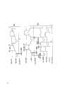
图1(a)-1(i)用以说明宽屏幕电视机的不同显示格式;Figures 1(a)-1(i) illustrate different display formats for wide-screen televisions;
图2是根据本发明各个方面并且适宜按2fH进行水平扫描工作的宽屏幕电视机的方框图;Figure 2 is a block diagram of a widescreen television adapted to operate with horizontal scanning at 2fH in accordance with aspects of the present invention;
图3示出图2所示宽屏幕处理器的方框图;Fig. 3 shows the block diagram of wide-screen processor shown in Fig. 2;
图4是根据本发明各方面制造且适宜在1fH水平扫描下工作的宽屏电视机的方框图;Fig. 4 is a block diagram of a widescreen television adapted to operate with 1fH horizontal scanning made in accordance with aspects of the present invention;
图5是图4所示宽屏处理器的方框图;Fig. 5 is a block diagram of the widescreen processor shown in Fig. 4;
图6示出图3和图5共同使用的宽屏幕处理器详细的方框图;Figure 6 shows a detailed block diagram of the wide-screen processor commonly used in Figures 3 and 5;
图7示出图6所示的画中画处理器的方框图。FIG. 7 shows a block diagram of the picture-in-picture processor shown in FIG. 6 .
图8示出图6所示的门阵列的方框图,并示出主信号通路、辅助信号通路和输出信号通路;Figure 8 shows a block diagram of the gate array shown in Figure 6, and shows the main signal path, auxiliary signal path and output signal path;
图9和10示出有利于说明如图1(d)所示的用充分剪切削的信号显示格式产生过程的定时图;Figures 9 and 10 show timing diagrams useful for illustrating the generation of a display format with a fully clipped signal as shown in Figure 1(d);
图11详细示出图8的主信号通路的方框图;Fig. 11 shows in detail the block diagram of the main signal path of Fig. 8;
图12详细示出图8的辅助信号通路的方框图;Figure 12 is a block diagram detailing the auxiliary signal path of Figure 8;
图13示出图7的画中画处理器的定时和控制部分的方框图;Figure 13 shows a block diagram of the timing and control portion of the picture-in-picture processor of Figure 7;
图14示出用以产生在1fH/2fH转换中的内部2fH信号的电路方框图。Figure 14 shows a block diagram of the circuit used to generate the internal 2fH signal in the 1fH /2fH conversion.
图15示出图2所示的偏转电路的电路方框的组合图。FIG. 15 shows a combined circuit block diagram of the deflection circuit shown in FIG. 2. FIG.
图16示出图2所示的RGB接口的方框图。FIG. 16 shows a block diagram of the RGB interface shown in FIG. 2 .
图1的各部分示出了可按本发明的各种不同方案实施的单个和多个画面显示格式的一些而不是全部的各种组合。这里所选择的都是为便于说明按本发明的方案构成宽屏幕电视的特定电路而举出的例子。为便于说明和讨论起见,视频源或信号的传统显示格式宽高比通常被认为是4×3,视频源或信号的宽屏幕显示格式宽高比则通常假设为16×9。Portions of FIG. 1 illustrate some, but not all, various combinations of single and multiple picture display formats that may be implemented in accordance with various aspects of the present invention. All selected here are examples for the convenience of explaining the specific circuit that constitutes the wide-screen TV according to the scheme of the present invention. For purposes of illustration and discussion, the conventional display format aspect ratio of a video source or signal is generally assumed to be 4×3, and the widescreen display format aspect ratio of a video source or signal is generally assumed to be 16×9.
图1(a)示出了传统的显示格式比为4×3的直观或投影电视。当16×9显示格式比的画面作为4×3显示格式比信号传输时,屏幕顶部和底部出现黑色条纹,这通常被称为信箱格式。这时所看到的画面要比整个可利用的显示区小一些。不然,也可以在传输之前将16×9显示格式比的信号源加以变换,从而使其在垂直方向填满4×3格式显示幅面。但这样就会有许多信息可能从左边和/或右边被剪切掉。作为另一种选择,可以将信箱式的画面在垂直方向上不扩展,但在水平方向上不扩展,这样得出的画面就会因垂直方面延长而产生畸变。这三种办法都没有特别可取之处。Figure 1(a) shows a conventional direct-view or projection television with a display format ratio of 4×3. When a 16×9 display format picture is transmitted as a 4×3 display format signal, black stripes appear at the top and bottom of the screen, which is commonly referred to as a letterbox format. The picture seen at this time is smaller than the entire available display area. Otherwise, the signal source with a display format ratio of 16×9 can also be converted before transmission, so that it can fill the display format of 4×3 format in the vertical direction. But then a lot of information may be cut off from the left and/or right. Alternatively, the letterboxed picture may be unexpanded vertically, but not expanded horizontally, so that the resulting picture would be distorted by the vertical elongation. None of these three approaches is particularly desirable.
图1(b)示出了16×9的屏幕。16×9显示格式比的视频源被全面显示出来,而不被剪切也没有畸变。16×9显示格式比的信箱式画面本身是在4×3显示格式比的信号中,这种画面可通过行加倍或加行的方法逐行扫描,以提供有足够垂直清晰度的较大幅面显示。无论信号源是主信号源、辅助信号源还是外部的RGB源,本发明的宽屏幕电视都能显示这种16×9显示格式比的信号。Figure 1(b) shows a 16×9 screen. Video sources with a 16×9 display format ratio are fully displayed without clipping or distortion. A 16x9 letterbox picture is itself in a 4x3 display format signal, which can be scanned progressively by doubling or adding lines to provide a larger format with sufficient vertical resolution show. No matter the signal source is the main signal source, the auxiliary signal source or the external RGB source, the wide-screen TV of the present invention can display the signal with the display format ratio of 16×9.
图1(c)示出了16×9显示格式比的主信号,其中一幅4×3显示格式比的插图也被显示。若主视频信号和辅助视频信号都是16×9显示格式比信号源,则插图的显示格式比也可以为16×9。插图可显示在许多的不同位置。Figure 1(c) shows the main signal for a 16x9 display format ratio, where an inset for a 4x3 display format ratio is also shown. If both the main video signal and the auxiliary video signal are signal sources with a display format ratio of 16×9, the display format ratio of the illustration can also be 16×9. Insets can be displayed in many different positions.
图1(d)示出一种显示格式,其中主视频信号和辅助视频信号都用相同幅面的画面显示出来。各显示区的显示格式比都是8×9,这当然和16×9及4×3的显示格式比不同。为在这样的显示区里显示4×3显示格式比的信号源而不致产生水平或垂直畸变,信号必然在左侧和/或右侧被剪切。如果容许宽高比由于画面在水平方向上受挤压而有些畸变,则可以显示出更多的、其画幅受较少剪切的画面。水平挤压使画面中的物体在垂直方向上拉长。本发明的宽屏幕电视能提供“剪切”和“宽高比畸变”这二者从最大程度的“剪切”与无“宽高比畸变”到无“剪切”与最大程度的“宽高比畸变”的任何一种组合情况。Fig. 1(d) shows a display format in which both the main video signal and the auxiliary video signal are displayed in the same frame size. The display format ratio of each display area is 8×9, which is of course different from the display format ratios of 16×9 and 4×3. In order to display a 4x3 display format ratio source in such a display area without horizontal or vertical distortion, the signal must be clipped on the left and/or right. If the aspect ratio is allowed to be somewhat distorted due to horizontal squashing of the picture, more pictures can be shown with less cropping of its frame. Squeeze horizontally to elongate objects in the frame vertically. Widescreen televisions of the present invention can provide both "cropping" and "aspect ratio distortion" from maximum "cropping" and no "aspect ratio distortion" to no "cropping" and maximum "width Any combination of high ratio distortion".
辅助视频信号处理通路中对数据取样的种种限制,对于产生高清晰度而画面的幅面象主视频信号产生的显示画面一样大的问题变得复杂化。为了克服这些复杂化现以研究出了各种不同的方法。The constraints on data sampling in the auxiliary video signal processing path complicate the problem of producing high definition pictures as large in format as the display produced by the main video signal. Various methods have been developed to overcome these complications.
图1(e)示出一种显示格式,在16×9显示格式比的屏幕居中部位显示出一幅4×3显示格式比的画面。右侧和左侧上的黑条可明显看到。Figure 1(e) shows a display format, in which a picture with a display format ratio of 4×3 is displayed at the center of the screen with a display format ratio of 16×9. The black bars on the right and left sides are clearly visible.
图1(f)示出一种显示格式,同时显示出一个4×3显示格式比的较大画面和三个4×3显示格式比的较小画面。在大画面周边外有较小画面的显示格式有时叫做POP,即“画外画”,而不是PIP(“画中画”)。在这里,两种显示格式都采用PIP或“画中画”一词。在宽屏幕电视设有两个调谐器的场合,无论两个调谐器都设在内部或一内一外地配置(例如盒式录象机中),就可以使各显示图象中的两个被显示画面显示出与信号源一致的实时动作。其余的画面可以按停帧格式显示。可以理解,增设另外的调谐器和另外的辅助信号处理通路可以提供两个以上的活动的画面。还可以理解,大画面和三个小画面的位置是可以对调的,如图1(g)所示。Fig. 1(f) shows a display format which simultaneously displays one larger frame with a 4x3 display format ratio and three smaller frames with a 4x3 display format ratio. A display format with a smaller frame around the perimeter of the larger frame is sometimes called POP, for "picture outside picture," rather than PIP ("picture in picture"). Here, both display formats use the term PIP, or "picture-in-picture." In the case where the wide-screen TV has two tuners, no matter whether the two tuners are arranged inside or one inside and one outside (such as in a video cassette recorder), two of the displayed images can be displayed. The display shows real-time action consistent with the source. The remaining pictures can be displayed in freeze frame format. It will be appreciated that the addition of additional tuners and additional auxiliary signal processing paths may provide more than two active pictures. It can also be understood that the positions of the large picture and the three small pictures can be swapped, as shown in Figure 1(g).
图1(h)示出的另一种显示格式是:一个4×3显示格式比的画在中间,两个纵列的、每个纵列有6个4×3显示格式比的较小画面排在两边每一侧上。和上述格式一样,有两个调谐器的宽屏幕电视能提供两个活动的画面。其余的11个图象就以停帧的格式显示。Another display format shown in Figure 1(h) is: a 4×3 display format ratio picture in the middle, two columns, each column has 6 smaller pictures with a 4×3 display format ratio Row on each side. As with the above formats, a widescreen TV with two tuners can provide two moving pictures. The remaining 11 images are displayed in freeze frame format.
图1(i)示出了由12个4×3显示格式比画面组成的格子的显示格式。这种显示格式特别适合作为频道选择指南,其中各画面至少是一个来自一个不同频道的停帧。和前面一样,正活动的画面的数目取决于可使用的调谐器和信号处理通路的数目。Fig. 1(i) shows the display format of a lattice composed of 12 4×3 display format ratio pictures. This display format is particularly suitable as a channel selection guide, where each picture is at least one freeze frame from a different channel. As before, the number of active pictures depends on the number of tuners and signal processing paths available.
图1所示的各种不同格式只是举例说明而已,并不局限于这些,这些格式可按下面各附图所示和下面即将被详细描述的宽屏幕电视加以实施。The various formats shown in Figure 1 are illustrative only and are not limiting and may be implemented in wide screen television as shown in the following figures and described in detail below.
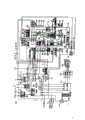
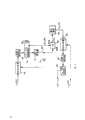
图2示出了本发明适宜以2fH水平扫描方式工作的宽屏幕电视机的方框图,其总编号为10。宽屏幕电视机10通常包括视频信号输入部分20、底盘或电视微处理器216、宽屏幕处理器30、1fH/2fH转换器40、偏转电路50、RGB接口60、YUV/RGB转换器240、显像管驱动器242、直观或投影显像管244和电源70。将各种电路分组成不同的功能块是为了便于描述,并不希望因此而限制了这些电路相互的物理位置。FIG. 2 shows a block diagram of a wide-screen television set suitable for working in a 2fH horizontal scanning mode according to the present invention, and its general number is 10. Wide-screen television set 10 generally includes video signal input part 20, chassis or
视频信号输入部分20适合用以接收来自不同视频源的多个复合视频信号。各视频信号可有选择地加以切换,以便将它们作为主视频信号和辅助视频信号显示。射频开关204有两个天线输入端天线1和天线2。这些分别是接收广播天线接收和电缆接收的输入端。射频开关204控制其中哪一个输入被提供到第一调谐器206及第二调谐器208(图3)。第一调谐器206的输出端即为单芯片202的输入端,单芯片202履行与调谐、水平和垂直偏转以及视频控制有关的很多功能。图中所示的特定的单芯片在工业上叫做TA7730型芯片。单芯片中起因来于自第一调谐器206的信号而产生的基带视频信号(VIDEO OUT)输出以供给到视频开关200和宽屏幕处理器30 TVI的输入端。其它输入到视频开关200的基带视频输入为AUX1和AUX2。它们可供摄像机、激光唱盘播放机、录像带播放机、电子游戏机等使用。视频开关200的输出由底盘或电视微处理器216控制,指定为(已切换的视频)(SWI TCHED VIDEO)。已切换的视频是宽屏幕处理器30的另一个输入。The video signal input section 20 is adapted to receive a plurality of composite video signals from different video sources. The video signals can be selectively switched so that they are displayed as main video signals and auxiliary video signals. The
再参看图3。开关SW1宽屏幕处理器将TV1和已切换的视频这两个信号之一选择作为选定输出(SEL COMP OUT)视频信号,这是Y/C译码器210的一个输入信号。Y/C译码器210可以是自适应行梳状滤波器。另外的两个视频源S1和S2也是Y/C译码器210的输入。S1和S2各表示不同的S-VHS源,它们各由分开的亮度信号和色度信号组成。有一个可作为Y/C译码器(如某些自适应行梳状滤波器)的一部分或作为分立开关的开关,它响应于电视微处理器216,以选取一对亮度和色度信号分别作为Y_M和C_IN的输出。所选出的一对亮度和亮度信号以后就作为主信号,并沿主信号通路进行处理。信号名中包含有_M或_MN的信号名是指主信号通路。宽屏幕处理器把亮度信号C_IN重新引回单芯片,以产生色差信号U_M和V_M。这里,U相当于(R-Y),V相当于(B-Y)。Y_M,U_M和V_M信号在宽屏幕处理器中被转换成数字形式以便在下一步进行信号处理。See Figure 3 again. The switch SW1 widescreen processor selects one of the two signals TV1 and switched video as the selected output (SEL COMP OUT) video signal, which is an input signal to the Y/
第二调谐器208在功能上属于宽屏幕处理器30的一部,它产生基带视频信号TV2。开关SW2从TV2和已切换的视频两个信号之间选择一个信号作为Y/C解码器220的一个输入。Y/C译码器220可以是自适应行梳状滤波器。开关SW3和SW4分别从Y/C译码器220的亮度和色度输出与来自外视频源的亮度和色度信号分别称为Y_EXT和C_EXT或Y_M和C_IN之间选择信号。Y_EXT和C_EXT信号对应于S_VHS输入S1。Y/C译码器220和开关SW3和SW4可以象在某些自适应梳状滤波器一样结合在一起。此后就将开关SW3和SW4的输出作为辅助信号并沿辅助信号通路进行处理。所选取的亮度输出称为Y_A。标有_A、_AX和_AUX信号的指的是辅助信号通路。所选取的色度输出被转换成色差信号U_A和V_A。Y_A、U_A和V_A信号被转换成数字形式以便进一步进行信号处理。在主信号和辅助信号通路上对视频信号源的切换设计使得对不同图象显示格式的各个不同部分的信号源选择的管理过程达到最大的灵活性。The
宽屏处理器给同步分离器212提供对应于Y_M的复合同步信号(COMP SYNC)。水平和垂直同步分量H和V分别作为垂直递减计数电路214的输入。垂直递减计数电路产生垂直复位(VERTCAL RESET)信号直接加到宽屏幕处理器30中。宽屏幕处理器产生内垂直复位输出信号(INT VERT RST OUT)并直接加到RGB接口60。RGB接口中的一个开关从内垂直复位输出信号与外RGB源的垂直同步分量之间选取信号。该开关的输出是经选择的垂直同步分量(SEL_VERT_SYNC)直接引到偏转电路50。辅助视频信号的水平和垂直同步信号由宽屏幕处理器中的垂直/水平同步译码器或同步分离器250(图3)产生。The widescreen processor supplies sync separator 212 with a composite sync signal (COMP SYNC) corresponding to Y_M. The horizontal and vertical sync components H and V serve as inputs to the vertical count down circuit 214, respectively. The vertical countdown circuit generates a vertical reset (VERTCAL RESET) signal that is directly added to the wide-
1fH/2fH转换器40用以将隔行扫描视频信号转换成逐行扫描的非隔行扫描信号,例如那种各水平行显示两次或通过内插同场的毗邻水平行产生另一组水平行的信号。在某些情况下,使用上一行或使用内插行取决于在毗邻各场或各帧之间检测出的动作程度(the level of movement)。转换电路40与视频RAM 420联合工作。视频RAM可用以存储一帧中的一场或多个场,以便能够逐行显示。经转换的视频数据为Y_2fH、U_2fH和V_2fH加到RGB接口60上。The 1fH /2fH converter 40 is used to convert an interlaced video signal into a progressive non-interlaced signal, such as one in which each horizontal line is displayed twice or another set of horizontal lines is generated by interpolating adjacent horizontal lines of the same field. OK signal. In some cases, the use of the previous line or the use of an interpolated line depends on the level of movement detected between adjacent fields or frames.
在图16中更详细地示出的RGB接口60使得可以将经转换的视频数据或外RGB视频数据供视频信号输入部分选取以便供显示用。外RGB信号可视为适宜供2fH扫描的宽显示格式比信号。宽屏幕处理器将主信号的垂直同步分量作为内垂直复位输出供到RGB接口,使偏转电路50可获得经选取的垂直同步信号(fvm或fvext)。宽屏幕电视工作允许使用者就可以通过产生内/外控制信号(INT/EXT)选取外RGB信号。但在没有外RGB信号的情况下选取外RGB信号输入时会使光栅在垂直方向上消失而且损坏阴极射线管或投影显像管。因此为了不致在没有该信号情况下选取外RGB输入,RGB接口电路对外同步信号进行检测。WSP微处理器340还提供用以控制外RGB信号的彩色控制和色调控制。The RGB interface 60, shown in more detail in Figure 16, allows converted video data or external RGB video data to be selected by the video signal input section for display. The external RGB signal can be regarded as a wide display format ratio signal suitable for 2fH scanning. The widescreen processor supplies the vertical sync component of the main signal to the RGB interface as an internal vertical reset output, so that the
宽屏幕处理器30包括画中画处理器320用以对辅助视频信号进行特殊的信号处理。“画中画”一词有时缩写成PIP或pix-in-pix。门阵列300将主和辅助视频信号数据组合成各式各样的显示格式,如图1(b)至1(i)的实例所示。画中画电路320和门阵列300受宽屏幕微处理器(WSPμP)340的控制。微处理器340经串行TV总线响应TV微处理器(TV μ P)216。串行TV总线包括四条信号线,供数据、时钟信号、启动信号和复位信号用。宽屏幕处理器30还产生复合垂直消隐/复位信号作为三电平砂堡信号(three level sandcastle signal)。不然,垂直消隐和复位信号也可以作为单独的信号分开产生。复合消隐信号由视频信号输入部分供到RGB接口。The
偏转电路50(详细示于图15中)接收来自RGB接口60的垂直复位信号、来自RGB接口60的选定的2f水平同步信号和来自宽屏幕处理器的另一些控制信号。在某些应用中垂直复位信号的路由可以从RGB60接口经过宽屏幕处理器30来。这些附加的控制信号涉及水平定相位、垂直尺寸调整和东-西枕形畸变调整(east-west pin adjustment)。偏转电路50将2fH回扫脉冲供到宽屏幕处理器30、将1fH/2fH转换器40、以及YUV/RGB转换器240上。Deflection circuit 50 (shown in detail in Figure 15) receives a vertical reset signal from RGB interface 60, a selected 2f horizontal sync signal from RGB interface 60 and other control signals from the wide screen processor. The vertical reset signal may be routed from the RGB60 interface through the
由交流市电供电的电源70产生整个宽屏幕电视的工作电压。A
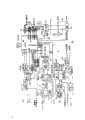
图3示出了宽屏幕处理器30的细节。宽屏幕处理器的主要部件有门阵列300、画中画电路301、模/数和数/模转换器、第二调谐器208、宽屏幕处理器微处理器(WSPμP)340和宽屏幕输出Y/C编码器227。图6示出了宽屏幕处理器更详细的细节(例如PIP电路),这对1f和2f底盘是共用的。图7示出了构成PIP电路301主要部分的画中画处理器320的细节。图8示出了门阵列300的细节。图3所示构成主信号通路和辅助信号通路各部分的一系列部件,这些都已详细描述过了。FIG. 3 shows details of the
第二调谐器208与中频级224以及声频级226连接。第二调谐器208还与WSP μ P340一起工作。WSP μ P 340包括输入/输出(I/O)部分340A和模拟输出部分340B。I/O部分340A提供色调和彩色控制信号、用以选择外RGB视频源用的内/外(INT/EXT)信号、和开关SW1和SW6的控制信号。I/O部分还监控来自RGB接口的外同步检测(EXT SYNC DET)信号,以保护偏转电路和阴极射线管。模拟输出部分340B通过各接口电路254、256和258提供垂直尺寸、东西调整和水平相位的控制信号。The
门阵列300负责把来自主信号和辅助信号通路的视频信息组合起来以实现复合宽屏幕显示,例如图1各不同部分所示的显示中的一种。锁相环374与低通滤波器376一起工作,提供门阵列的时钟脉冲信息。主视频信号作为Y_M、U_M和V_M信号以模拟的形式和YUV格式供到宽屏幕处理器上。这些主信号由图6中更详细示出的模/数转换器(A/D)342和346从模拟形式转换成数字形式。
彩色分量信号通常用U和V表示,这些信号可分配给R-Y或B-Y信号或者可分配给I和Q信号。所取样的亮度带宽限制在8MHz,这是因为系统时钟频率为1024fH,这大约为16MHz。由于宽度为I时U和V信号限制在500KHz或1.5MHz,所以对彩色分量数据进行取样时可采用单个模/数转换器和一个模拟开关。模拟开关或复用器344的选择线UV_MUX是将系统时钟除以2得到的8MHz信号。具有一个时钟信号宽度的行开始脉冲(SOL)同步地使该信号在各水平视频行开始时复位到0。UV_MUX线于是在整个水平行内的每个时钟周期翻转其状态。由于行长等于偶数个时钟周期,因而UV_MUX的状态一经初始化就会不中断地始终进行翻转:0,1,0,1,…。由于各模/数转换器242和346都有1个时钟周期的时延,因而从模/数转换器342和346出来的Y和UV数据流都进行移位。为适应这个数据移位,来自主信号处理通路304的时钟选通信息也必须同样地延迟。如果时钟选通信息不延迟,在UV数据被删除时不会正确成对。这一点很重要,因为各UV对代表一个向量。在不引起彩色偏移的情况下,一个向量的U分量不能与另一向量的V分量配对。相反,前一对的V样品会连同当前的U样品一齐被删除。由于每对彩色分量(U,V)样品有两个亮度样品,所以这种UV复用的方法叫做2∶1∶1。这时就有效地使U和V两者的奈奎斯频率降低为亮度奈奎斯特频率的一半。因此对于亮度分量的模/数转换器输出的奈奎斯频率为8MHz,而对于彩色分量的模/数转换器输出的奈奎斯频率为4MHz。The color component signals are usually denoted U and V, and these signals may be assigned to RY or BY signals or may be assigned to I and Q signals. The sampled luminance bandwidth is limited to 8MHz because the system clock frequency is 1024fH , which is about 16MHz. Since the U and V signals are limited to 500KHz or 1.5MHz when the width is I, a single A/D converter and an analog switch can be used for sampling the color component data. The select line UV_MUX of the analog switch or
画中画电路和/或门阵列还可包括用以在数据被压缩的情况下也能提高辅助数据清晰度的装置。迄今已研究出很多数据缩减和数据恢复方案,包括例如成对象素压缩和抖颤调谐(dithering)及去抖颤调谐(dedithering)。此外还考虑涉及不同比特个数的不同抖颤调谐序列和涉及不同比特个数的不同成对象素压缩。WSP μ P340可以选取很多特定数据缩减和恢复方案中的一个方案,以使各特定种类的画面显示格式所显示的视频达到最高的清晰度。The picture-in-picture circuit and/or gate array may also include means for improving the clarity of the auxiliary data even if the data is compressed. Many data reduction and data recovery schemes have been studied to date, including eg pairwise pixel compression and dithering and dedithering. Also considered are different dither tuning sequences involving different numbers of bits and different pairwise pixel compressions involving different numbers of bits. The WSP μ P340 can select one of many specific data reduction and restoration schemes to achieve the highest resolution video displayed for each specific type of picture display format.
门阵列包括与各个行存储器一起工作的一些内插器,各个行存储器则可以是FIFO 356和358。内插器和FIFO用以在必要时对主信号进行再取样。一个附加的内插器可对辅助信号再取样。门阵列中的时钟和同步电路控制主信号和辅助信号两者的数据管理过程,包括将它们组成具有Y_MX、U_MX和V_MX分量的单个输出视频信号。这些输出分量由数/模(D/A)转换器360、362和364转换成模拟形式。称为Y、U和V的模拟形式的信号加到1fH/2fH转换器40上以便转换成非隔行扫描方式。Y、U和V信号还由编码器227编码成Y/C格式,以限定的宽格式比输出信号Y_OUT_EXT/C_OUT-EXT在面板插孔处可获取。开关SW5给编码器227从门阵列选择同步信号C_SYNC-MN,或从PIP电路选择同步信号C_SYNC-AUX。开关SW6从Y_M和C_SYNC_AUX二者之间选择信号作为宽屏幕面板输出的同步信号。The gate array includes interpolators working with the respective row memories, which in turn may be FIFOs 356 and 358 . Interpolators and FIFOs are used to resample the main signal when necessary. An additional interpolator resamples the auxiliary signal. Clock and synchronization circuits in the gate array control the data management process for both the main and auxiliary signals, including composing them into a single output video signal with Y_MX, U_MX and V_MX components. These output components are converted to analog form by digital-to-analog (D/A)
图14示出水平同步电路的各部分的细节。相位比较器228是包括低通滤波器230、压控振荡器232、除法器234和电容器236在内的锁相环的一部分。压控振荡器232响应陶瓷谐振器或类似的器件238,以32fH工作。压控振荡器的输出被除以32,以向相位比较器228提供一合适频率第二输入信号。除波器234的输出为1fHREF定时信号。32fHREF和1fHREF定时信号施加至除16计数器400上。2fH输出被加到脉宽电路402上。由1fHREF预置的除法器400保证该除法器与视频信号输入部分的锁相环同步地工作。脉宽电路402保证2fH-REF将有一个适当的脉宽,以保证例如CA1391型的相位比较器404适当的工作,该相位比较器404形成包括低通滤波器406和2fH压控振荡器408的第二锁相环的一部分。压控振荡器408产生内2fH定时信号,该定时信号用以驱动逐行扫描显示。输入至相位比较器404的其他输入信号是2fH回扫脉冲或与其有关的定时信号。采用包括相位比较器404的第二锁相环,有利于保证在输入信号的每个1fH周期内各2fH扫描周期是对称的。否则,显示会出现屏面撕裂,例如其中一半视频行移至右面,而另一半视频行移至左面。Fig. 14 shows details of various parts of the horizontal synchronization circuit.
图15示出偏转电路50的细节。设置电路500用以根据实现不同的显示格式所需要的垂直过扫描量调节光栅的垂直方向尺寸。如示意图所示,恒流源502提供恒量的电流I斜坡给垂直斜波电容器504充电。晶体管506与垂直斜波电容器并联连接,响应垂直复位信号,周期性地给该电容器放电。在不进行任何调节的情况下,电流I斜坡使光栅的垂直方向尺寸达到能达到的最大值。这可能相当于当一个扩展的4×3显示格式比信号源充满宽屏幕显示器(如图1a中所示)时所需要的垂直过扫描量。在所要求的光栅垂直方向尺寸较小的情况下,可调电流源508从I斜坡把可变的电流量I调整从I斜坡转移开,从而使垂直斜波电容器504缓慢充电到较小峰值。可调电流源508响应垂直尺寸控制电路所产生的例如为模拟形式的垂直尺寸调整信号。垂直尺寸调整电路500与手动垂直尺寸调整电路510无关,后者可以是一个电位器或后面板调节钮。在上述两者中的任一种情况之下,垂直偏转线圈512都接收适量的驱动电流。水平偏转由相位调整电路518、东-西枕形畸变校正电路514、2fH锁相环520和水平输出电路516提供。FIG. 15 shows details of the
图16更详细地示出了RGB接口电路60的细节。最后被显示的信号在1fH/2fH转换器40的输出与外RGB的输入两者之间选择。对于这里所描述的宽屏幕电视而言,假设外RGB的输入为宽格式显示比的逐行扫描源。来自视频信号输入部分20的复合消隐信号和外RGB信号输入到RGB-YUV转换器610。外RGB信号的外2fH复合同步信号被用来作为外同步信号分离器600的输入。垂直同步信号的选择由开关608执行。选择水平同步信号是由开关604来执行。选择视频信号是由开关606来执行。各开关604、606和608响应WSP μ P340所产生的内/外控制信号。内或外视频源的选择由使用者进行。但若使用者无意中选择外RGB源,当未接有或未调谐在这种信号源时或如果外信号源失落时,则垂直光栅会消失,于是会给阴极射线管造成严重的损坏。因此外同步检测器602检测有否外同步信号存在。没有这种信号时,就有一个“开关拒绝控制”信号传送到各开关604、606和608上,以在没有这种信号时防止选择外RGB源。RGB/YUV转换器610还接收来自WSP μ P340的色调和彩色控制信号。Figure 16 shows details of the RGB interface circuit 60 in more detail. The final displayed signal is selected between the output of the 1fH /2fH converter 40 and the input of the external RGB. For the wide-screen television described here, it is assumed that the external RGB input is a wide format display ratio progressive scan source. The composite blanking signal and the external RGB signal from the video signal input section 20 are input to the RGB-
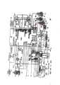
根据本发明的方案且适宜在1fH水平扫描操作的宽屏幕电视机的总方框图示于图4,且总标号为11。大体上对应于图2中所示的电视机10中的电视机11的那些部件使用相同的标号。电视机11通常包括视频信号输入部分21、底盘或TV微处理器(μP)216、宽屏幕处理器31、水平偏转电路52、垂直偏转电路56、RGB矩阵变换电路241、显像管驱动器242、直观或投影显像管244和一电源70。这里没用1fH/2fH转换器和RGB接口,因此如就没有用于以2fH扫描速率显示外宽格式显示比RGB信号的设备。将各此电路分为不同的功能块,目的是为了便于描述,并不是限制这些电路相互间相对的特理位置。A general block diagram of a wide screen television set according to the aspects of the invention and adapted to operate at 1fH horizontal scanning is shown in FIG. 4 and generally designated 11 . Components corresponding substantially to those of
视频信号输入部分21自适应接收来自不同视频源的多个复合视频信号。视频信号可以有选择地被切换以作为主视频信号和辅助视频信号来显示。射频开关204有两个天线输入端天线1和天线2。它们代表停播天线接收和电缆接收。射频开关204控制哪一个天线输入被加到第一调谐器206和第二调谐器208。第一调谐器206的输出是单芯片203的输入,该芯片203执行有关调谐、水平和垂直偏转以及视频控制的多种功能。所示的特定单芯片是工业上叫做TA8680型芯片。在单芯片中产生且由于来自第一调谐器器206的信号产生的基带视频信号(VI DEO OUT)是一输入至视频开关200和宽屏幕处理器31的TV1两者的输入端输入信号。其他输入至视频开关200的基带视频输入信号为AUX1和AUX2。这些输入端可用于摄像机、录像机或类似的装置。由底盘或TVμ216控制的视频开关200的输出为已切换的视频(SWI TCHED VI DEO)。它是宽屏幕处理器31的另一个输入。The video
再参阅图5,宽屏幕处理器的开关SW1在信号TV1和已切换视频两者之间选择,出“选定复合输出”(SEL COMP OUT)视频信号,作为Y/C译码器210的一个输入。该Y/C译码器210可以实施为一个自适应行梳状滤波器。另一个视频源S1也是Y/C译码器210的输入。源S1表示一个S-VHS源,且包括分离的亮度信号和色度信号。一个开关可以作为Y/C译码器210(如某些自适应行梳状滤波器)的一部分,或实施为一个分立开关,它响应TVμ216以选取一对亮度和色度信号分别作为Y_M和C_IN的输出。所选出的这一对亮度和色度信号然后就作为主信号沿主信号通路进行处理。宽屏幕处理器内的译码器/解调器产生色差信号U_M和V_M。Y_M、U_M和V_M信号在宽屏幕处理器中被转换成数字形式,以便在门阵列300中作下一步信号处理。Referring to Fig. 5 again, the switch SW1 of the wide-screen processor selects between the signal TV1 and the switched video, and outputs the "selected composite output" (SEL COMP OUT) video signal, which is used as one of the Y/
第二调谐器208在功能上被限定为宽屏幕处理器30的一部分,它产生基带视频信号TV2。开关SW2在TV2和已切换视频两信号之间选择一个信号作为Y/C译码器220的输入。Y/C译码器220可实施为一个自适应行梳状滤波器。开关SW3和SW4分别从Y/C译码器220的亮度和色度输出与来自外视频源的亮度信号Y_EXT和色度信号C_EXT之间选择信号。Y_EXT和C_EXT信号对应于S_VHS输入S1。Y/C译码器220和开关SW3和SW4可以象在某些自适应梳状滤波器一样相组合。此后将开关SW3和SW4的输出作为辅助信号并沿辅助信号通路进行处理。所选取的亮度输出为Y_A。标有_A,_AX和_AUX信号名的指的是辅助信号通路。所选取的色度输出被转换成色差信号U_A和V_A。Y_A、U_A和V_A信号被转换成数字形式以便下一步信号处理。在主信号和辅助信号通路上对视频信号源的切换的安排使得对不同画面显示格式的各个不同部分的信号源选择的管理过程达到最大的灵活性。The
宽屏幕处理器30包括画中画处理器320用以对辅助视频信号进行特殊的信号处理。“画中画”一词有时缩写成PIP或pix-in-pix。门阵列300将主和辅助视频信号数据组合成各式各样的显示格式,如图1(b)至1(i)的实例所示。画中画电路320和门阵列300受宽屏幕微处理器WSP μ P340的控制。WSP μ P 340经由串行TV总线而响应TVμP216。串行总线包括四条信号线,供数据、时钟信号、启动信号和复位信号用。宽屏幕处理器30还产生复合垂直消隐/复位信号作为三电平砂堡信号(three level sandcastle signal)。不然,垂直消隐和复位信号也可以作为单独的信号分开产生。复合消隐信号由视频信号输入部分供到RGB接口。The
主信号的水平和垂直同步分量在同步分离器286中产生,该分离器286形成解调器288的部分,而解调器288形成宽屏幕处理器的部分。水平同步分量是1fH锁相环290的输入。辅助图象信号的水平和垂直同步信号是通过宽屏幕处理器31中的同步分离器250形成的。水平偏转电路52响应来自WSP μ P 340的东/西枕形畸变调整和水平相位控制信号与单芯片一起工作。垂直偏转电路56响应垂直尺寸控制电路54。垂直尺寸控制电路54响应来自WSP μ P 340的垂直尺寸控制信号,而以类似于上述2fH底盘的垂直尺寸控制的方式工作。The horizontal and vertical sync components of the main signal are generated in a
图5示出了宽屏幕处理器31的细节。宽屏幕处理器的主要部件有门阵列300、画中画电路301、模/数和数/模转换器,第二调谐器208、宽屏幕处理器微处理器WSP μ P 340和宽屏幕输出编码器227。图6示出了宽屏幕处理器更详细的细节,该处理器对1fH和2fH底盘(例如画中画电路)是共用的。图7更详细地示出了画中画电路301主要部分的画中画处理器320。图8更详细地示出了门阵列300。图3所示构成主信号通路和辅助信号通路各部分的一系列部件已详细介绍过。一些其他的部件例如第二调谐器208、WSP μ P 340和接口输出端、模/数和数/模转换器、门阵列300、画中画电路301及锁相环374大体上按图3所说明的工作,而那些细节不再重复。FIG. 5 shows details of the
主视频信号Y_M和C_IN以模拟方式供给宽屏幕处理器。信号C_IN由解调器288解码成色差信号U_M和V_M。主信号由模/数转换器342和346(详细地示于图6中)从模拟形式转换成数字形式。辅助视频数据也以模拟方式及YUV格式作为Y_A、U_A和V_A的信号。在画中画电路301中,这些辅助信号被转换成数字形式、被数据压缩、与主信号同步地存储场存储器内,且提供给门阵列300以便按照选定的画面显示格式(例如在行到行的基础上复用)的要求与主信号相组合。画中画电路的操作可结合图6作更全面的说明。画中画电路和/或门阵列也可包括用以在数据压缩的情况下也能提高辅助数据的清晰度的装置。模拟形式信号Y、U和V供给编码器227,以限定宽格式比输出信号Y_OUT_EXT/C_OUT_EXT,如果是这样,这些信号被输入至单芯片203(图4)。编码器227只接收来自门阵列的C_SYNC_MN信号。开关SW5在Y_M和C_SYNC_AUX之间选择出作为输入到模/数转换器的输入信号。单芯片203产生RGB矩阵241用的YUV格式信号,该RGB矩阵241将来自Y_OUT_EXT和C_OUT_EXT信号的RGB格式信号供给显像管驱动器242。The main video signals Y_M and C_IN are supplied in analog to the widescreen processor. Signal C_IN is decoded by
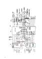
图6的方框图更详细地示出了分别在图3和图5中所示的对1fH和2fH底盘共用的宽屏处理器30和31的细节。Y_A、U_A和V_A信号为画中画处理器320的输入,处理器320可以包括清晰度处理电路370。根据本发明很多方面,宽屏幕电视机能将视频加以扩展和压缩。图1中部分示出的各种复合显示格式所体现的特殊效果是由画中画处理器320产生的,该处理器能接收来自清晰度处理电路370的经清晰度处理的数据信号Y_RP、U_RP和V_RP。并不是任何时候都要使用清晰度处理,但在显示格式已选好时就要使用。图7示出了画中画处理器320的细节。画中画处理器的主要部件有模/数转换器部分322、输入部分324、快速开关(FSW)和总线部分326、定时和控制部分328以及数/模转换部分330。图13示出了定时和控制部分328的细节。The block diagram of Figure 6 shows in greater detail the details of the
画中画处理器320可被看作是汤姆逊消费者电子设备公司研制的基本CPIP芯片的变种。这种处理器可使其具有很多特殊的特征或特殊的效果,下面举几个例子说明。基本的特殊效果是如图1(c)中所示的那种在一个大画面的已具有重叠在其上一部分的一个小画面。这种大小画面可从同一个视频信号产生,也可从不同的视频信号产生,还可以互换或更换。一般说来,伴音信号总是切换成使其对应于大画面。小画面可移到屏幕上的任何位置或逐步转入很多预定位置上。变焦距的特性使得小画面放大和缩小到例如任一预定的幅面。有时,例如在图1(d)所示的显示格式中,大小画面实际上是同一尺码。The picture-in-
在单画面方式下,例如在图1(b)、1(e)或1(f)所示的显示的,使用者可以例如逐步从1.0∶1至5.0∶1的比值将单画面的内容变焦。而在变焦方式下,使用者可以搜索或扫调整个画面内容,使屏面上的影象得以跨不同的画面区移动。在两者的情况下,无论是小画面、还是大画面或是变焦画面都可以以停帧的方式(静止画面格式)显示。这种功能可以实现选通显示格式,这时视频信号中的最后九个帧可以在屏幕上反复显示。帧重复率可以从30帧/秒改变到0帧/秒。In single-frame mode, such as those shown in Figures 1(b), 1(e) or 1(f), the user can zoom the contents of the single-frame, for example, stepwise from a ratio of 1.0:1 to 5.0:1 . In the zoom mode, the user can search or scan the entire screen content, so that the images on the screen can move across different screen areas. In both cases, whether it is a small picture, a large picture or a zoomed picture, it can be displayed in a freeze frame (still picture format). This feature enables strobe display formats, where the last nine frames of the video signal are displayed repeatedly on the screen. The frame repetition rate can be changed from 30 fps to 0 fps.
本发明另一方案的宽屏幕电视机中所使用的画中画处理器与上述基本CPIP芯片的现行结构不同。若基本CPIP芯片与16X9屏幕的电视机配用而不用视频增速电路的话,则由于横贯较宽的16×9屏幕扫描而致使实际水平方向扩展4/3倍,因而使插图呈现出宽高比畸变。于是画面中的实物可能在水平方向拉长。若采用外增速电路,则不会有宽高比畸变,但画面会占不满整个屏幕。The picture-in-picture processor used in the wide-screen TV of another solution of the present invention is different from the current structure of the above-mentioned basic CPIP chip. If the basic CPIP chip is used with a TV set with a 16X9 screen without a video booster circuit, the actual horizontal expansion will be 4/3 times due to scanning across the wider 16X9 screen, thus making the illustration appear in an aspect ratio distortion. Therefore, the real object in the picture may be elongated in the horizontal direction. If an external speed-up circuit is used, there will be no aspect ratio distortion, but the picture will not occupy the entire screen.
以基本CPIP芯片为基础的现有的画中画处理器,像在常规电视机里应用一样,以特定的方式工作,有一此不良后果。输入视频以锁定在主视频源的水平同步信号上的640fH时钟取样。换言之,存储在与CPIP芯片相联的视频RAM中的数据,不是相对于输入辅助视频源进行正交取样。这是场同步的基本CPIP方法上的主要局限性。输入取样率的非正交性质导致取样数据的歪斜误差。该局限性是视频RAM与CPIP芯片一起使用的结果,该芯片必须采用相同的用以写和读数据的时钟。当来自视频RAM(例如视频RAM350)的数据被显示时,歪斜误差可从沿画面的垂直边缘的随机跳动看得出来,且通常被认为是完全不能接受的。Existing picture-in-picture processors based on basic CPIP chips, like those used in conventional televisions, work in a specific way, with one side effect. Input video is sampled with a 640fH clock locked to the main video source's horizontal sync signal. In other words, the data stored in the video RAM associated with the CPIP chip is not sampled in quadrature with respect to the input auxiliary video source. This is the main limitation on the basic CPIP approach of field synchronization. The non-orthogonal nature of the input sampling rate results in skew errors in the sampled data. This limitation is a result of using video RAM with CPIP chips, which must use the same clock for writing and reading data. When data from video RAM (such as video RAM 350) is displayed, skew errors can be seen as random jumps along the vertical edges of the picture and are generally considered to be completely unacceptable.
根据本发明的一个方案,画中画处理320与基本CPIP芯片不同,可自适应地按照多个可选择的显示方式中的一种对视频数据不对称压缩。在这种方式的操作中,各画面在水平方向上按4∶1压缩,在垂直方向上按3∶1压缩。为了在视频RAM内存储所做的这种不对称压缩方式会产生宽高比畸变的画面。该画面中的各实物在水平方向被挤压。但若这些画面正常地例如频道扫描方式被读出以供16×9显示格式比屏幕显示,则画面看起来正常。画面充满屏幕,且没有宽高比畸变。按照本发明这方面的不对称压缩方式使得在不用外增速电路的情况下在16×9的屏幕上产生特殊的显示格式成为可能。According to a solution of the present invention, the picture-in-
图13是画中画处理器(例如上述CPIP芯片的一种改型)的定时和控制部分328的方框图,该部分包括“十中取几”(decimation)电路328C,用以按照多个可选择的显示方式中的一个进行不对称压缩。其余的显示方式可以提供不同幅面的辅助画面。各水平和垂直“十中取几”电路都包括一个计数器,该计数器在WSP μ P340的控制下对于来自数值表的压缩因数进行编程序。数值的范围可以是1∶1、2∶1和3∶1等等。压缩因数可以是对称的或不对称的,取决于该表怎样编排。压缩比的控制也可按完全可编程的、通用的“十中取几”电路在WSP μ P340的控制下工作来实现。FIG. 13 is a block diagram of the timing and
在全屏幕画中画方式下,画中画处理器与自激振荡器348(图6)相结合,将从一个译码器(例如自适应梳状滤波器)取Y/C输入,将该信号译码成为Y、U、V彩色分量,并产生水平和垂直同步脉冲。这些信号在画中画处理器中处理以适合于诸如变焦、停帧和频道扫描等各种全屏幕显示方式。例如,在频道扫描显示方式期间,由于被取样的信号(不同频道)会有不相关的同步脉冲而且会在随机的瞬间及时加以切换,因此从视频信号输入部分提供的水平和垂直同步会有许多不连续之处。因此取样时钟和读/写视频RAM时钟由自激振荡器348来确定。在停帧和变焦方式下,取样时钟脉冲会锁定到输入视频的水平同步上,在这些特殊情况下,其与显示时钟频率相同。In full-screen picture-in-picture mode, the picture-in-picture processor combined with the free-running oscillator 348 (Fig. 6) will take the Y/C input from a decoder (such as an adaptive comb filter), The signal is decoded into Y, U, V color components and generates horizontal and vertical sync pulses. These signals are processed in the picture-in-picture processor for various full-screen display modes such as zoom, freeze frame and channel scan. For example, during channel scan display mode, the horizontal and vertical sync provided from the video signal input section will have many discontinuities. The sampling clock and the read/write video RAM clock are therefore determined by the
再参看图6,来自画中画处理器以模拟形式出现的Y、U、V和C_SYNC(复合同步)输出由编码电路366再编码成为Y/C分量,编码电路366与3.58MHz振荡器380联合工作。该Y/C_PIP_ENC信号可接到Y/C开关上(图中未示出),该开关使再编码后的Y/C分量可以代替主信号的Y/C分量。从这时起,经PIP编码的Y、U、V和同步信号成了底盘中其余部分的水平和垂直定时的基础。这种工作方式适宜根据主信号通路中内插器和FIFO的工作情况实施PIP的变焦显示方式。Referring again to FIG. 6, the Y, U, V, and C_SYNC (composite sync) outputs in analog form from the picture-in-picture processor are re-encoded into Y/C components by encoding circuit 366, which is associated with 3.58
在例如图1(i)所示的多频道方式下,预定的扫描表中的十二个频道可以由十二个小画面同时显示。画中画处理器具有响应3.58MHz振荡器348的一个内部时钟。输入辅助信号从模拟形式转换成数字形式,且响应选定的特殊用而被装入视频RAM350内。在上述技术训练手册的实施例中,编码的特殊作用是在与主信号视频数据组合之前在其中画处理器里被转换回到模拟形式。但在这里所述的宽屏电视机中,且部分由于可用的不同的时钟频率数目的限制,辅助数据不由画中画处理器320进一步处理,而直接从视频RAM350输出。时钟信号的数目的减少有利于在电视机的电路中可减小射频干扰。For example, in the multi-channel mode shown in FIG. 1(i), twelve channels in the predetermined scanning list can be simultaneously displayed by twelve small screens. The picture-in-picture processor has an internal clock responsive to the 3.58
再参看图7。画中画处理器320包括模/数转换部分322、输入部分324、快速开关(FSW)和总线控制部分326、定时和控制部分328和数/模转换部分330。通常,画中画处理器320将视频信号数字化成为亮度(Y)和色差信号(U,V),将所得结果进行次取样并存储在1兆比特的视频RAM350中,如上面所述的那样。与画中画处理器320相关的视频RAM350其存储容量为1兆比特,其容量大得足以存储带8比特样品的视频数据的一整场。增加存储的容量必然花费大,而且需要更复杂的管理电路。辅助频道中每单位样品的较少的比特个数意味着减少相对于主信号的量化清晰度或带宽,该主信号始终是按8比特样品进行处理的。实际上带宽的减小在辅助显示的画面较小时通常是不成问题,但若辅助显示画面较大时,例如与主显示画面的幅面相同时,就有问题。清晰度处理电路370(图6)可有选择地实施用以提高辅助视频数据量化清晰度或有效带宽的一种或多种方案。业已研究出很多数据缩减和数据恢复的方案,包括例如成对象素压缩和抖颤调谐及去抖颤调谐。令去抖颤调谐电路在工作时配置在视频RAM350下游处,例如在门阵列的辅助信号通路中,下面即将更详细地描述。此外,还可以考虑涉及不同位数的不同抖颤调谐及去抖颤调谐序列和涉及不同位数的不同成对象素压缩方案。为使各特种图象显示格式显示出来的图象达到最高的清晰度,可通过WSPμP从一系列减少和恢复数据的方案中选取一种方案。See Figure 7 again. The picture-in-
亮度和色差信号按8∶1∶1的六比特Y、U、V方式存储。也就是说,把各分量量化成六比特样品。每对色差样品有八个亮度样品。为此,画中画处理器320按照这样的方式工作,亦即输入的视频数据是以锁定到输入的辅助视频同步信号上的640fH时钟频率来取样的。在这种工作方式下,存储在视频RAM中的数据系正交取样的。当从画中画处理器的视频RAM350读数据时,该数据是利用锁定到输入的辅助视频信号上的同一个640fH时钟而读出的。然而,尽管这个数据是正交取样并被存储的,而且还能正交地被读出,由于主和辅助视频源的非同步性质,使该数据也不能从视频RAM350直接正交地显示。主视频和辅助视频源只有在它们是来自同一视频源的显示信号时才可以指望是同步的。The luminance and color difference signals are stored in a six-bit Y, U, V mode of 8:1:1. That is, each component is quantized into six-bit samples. There are eight luminance samples per pair of color difference samples. To this end, the picture-in-
为了使辅助频道(即从视频RAM350输出的数据)与主频道同步,需要进行下一步处理。再参看图6,两个四比特锁存器352A和352B用以重新组合来自视频RAM 4比特输出端的8比特数据块。该四比特锁存器还使数据时钟频率从1280fH降到640fH。In order to synchronize the auxiliary channel (ie, the output data from the video RAM 350) with the main channel, a further process is required. Referring again to FIG. 6, two four-bit latches 352A and 352B are used to reassemble the 8-bit data block from the 4-bit output of the video RAM. The four-bit latch also reduces the data clock frequency from 1280fH to 640fH .
通常,令视频显示和偏转系统与主视频信号同步。如上所述,必须对主视频信号加速,以充满宽屏幕显示器。必须使辅助视频信号与第一视频信号和视频显示器垂直同步。辅助视频信号可在场存储器中延迟不到一个场周期,然后在行存储器中加以扩展。辅助视频数据与主视频数据的同步化利用作为场存储器的视频RAM350和用以扩展该信号的先进先出(FIFO)行存储器354来实现。FIFO354的大小为2048×8。FIFO的大小与为避免读/写指针冲突而被认为是合理需要的最小的行存储容量有关。读/写指针冲突发生在新数据有机会写入FIFO之前从FIFO读出旧数据的时候。读/写指针发生冲突还发生在旧数据有机会从FIFO被读出之前新数据改写存储器的时候。Typically, the video display and deflection system are synchronized to the main video signal. As mentioned above, the main video signal must be sped up to fill the widescreen display. The auxiliary video signal must be vertically synchronized with the primary video signal and with the video display. The auxiliary video signal can be delayed by less than one field period in the field memory and then expanded in the line memory. Synchronization of auxiliary video data with main video data is accomplished using
来自视频RAM350的8比特DATA_PIP数据块以曾用来对视频数据进行取样的同一个画中画处理器的640fH时钟(即锁定到辅助信号而不是主信号上的)写入2048×8 FIFO 354中。FIF 354使用1024fH的显示时钟来读取,该时钟系锁定到主视频频道的水平同步分量上。使用具有独立读/写端口时钟的多行存储器(FIFO)就能使曾以第一速率正交取样的数据以第二速率正交地被显示。然而,读/写时钟脉冲的非同步性质要求采取措施来避免读/写指针的冲突。The 8-bit DATA_PIP data block from the
门阵列300由两个宽屏幕处理器30和31共用的。图8中以方框图的形式示出了主信号通路304、辅助信号通路306和输出信号通路312。门阵列还包括时钟/同步电路320′和WSPμP译码器310。WSPμP译码器310的数据和地址输出线(以WSP数据表示)施加到上述各主电路和主通路上,还加到画中画处理器320和清晰度处理电路370上的。应该理解的是,是否把一些电路作为还是不作为门阵列的一部分,主要考虑到解释本发明方案的便利。
门阵列用以在必要时扩展、压缩和剪切主视频频道的视频数据,以便实现不同的画面显示格式。亮度分量Y_MN存储在先进先出(FIFO)行存储器356中,存储时间的长短取决于亮度分量内插的情况。经组合的色度分量U/V-MN存储在FIFO 358中。辅助信号亮度和色度分量Y_PIP、U_PIP和V_PIP由去复用器355得出。必要时亮度分量在清晰度处理电路357中经过清晰度处理,然后在必要时由内插器359将其扩展,产生信号Y_AUX作为输出。The gate array is used to expand, compress and cut the video data of the main video channel when necessary, so as to realize different picture display formats. The luminance component Y_MN is stored in a first-in-first-out (FIFO)
在某些情况下,辅助信号显示与主信号显示一样大,图1(d)所示的就是一个例子。与画中画处理器和视频RAM350有关的存储限制会使提供的用以充满这种大型显示区所需要的数据压缩或象素数量不足。在这种情况下,可以用清晰度处理电路357将象素还给辅助视频信号中,以代替那些在数据压缩或缩减过程中失去的象素。该晰度处理可以对应于图6所示的清晰度处理电路370所进行的清晰度处理。例如,清晰度处理电路370可以是抖颤调谐电路,而清晰度处理电路357可以是去抖颤调谐电路。In some cases, the auxiliary signal display is as large as the main signal display, as shown in Figure 1(d) is an example. Memory limitations associated with the picture-in-picture processor and
辅助视频输入数据以640fH速率被取样,并被存储在视频RAM350中。辅助数据从视频RAM350里读出,在图中标作VRAM_OUT。画中画电路301也具有接相等的整数因数在水平和垂直方向上以及不对称地减小辅助画面的能力。再参阅图12,辅助频道数据由4比特锁存器352A和352B、辅助FIFO354、定时电路369以及同步电路368被缓冲并与主频道的数字视频同步。VRAM_OUT数据由去复用器355分成为Y(亮度)、U、V(彩色分量)和FSW_DAT(快速切换数据)。FSW_DAT表明哪种场型式被写入视频RAM。PIP_FSW信号直接从画中画电路接收,且施加在输出控制电路321上,以确定在小画面方式其间从视频RAM读出的哪一场将被显示出来。Auxiliary video input data is sampled at 640fH rate and stored in
辅助频道以640fH的速率被取样,主频道则以1024fH的速率被取样。辅助频道FIFO 354将数据从辅助频道取样率转换成主频道时钟频率。在此过程中,视频信号经过8/5(即1024/640)的压缩。这比正确显示辅助频道信号所需的4/3压缩还多。因此辅助频道必须借助于内插器359来扩展,以便正确显示4×3的小画面。内插器359由内插器控制电路371控制,后者本身响应WSPμP340。所需的内插器扩展量为5/6。扩展因数X按下式确定:The auxiliary channel is sampled at 640fH and the main channel is sampled at 1024fH. The
X=(640/1024)*(4/3)=5/6X=(640/1024)*(4/3)=5/6
色度分量U_PIP和V_PIP由延迟电路367(图8)加以延迟,延迟时间的长短取决于亮度分量内插的情况,产生信号U_AUX和V_AUX作为输出。主和辅助信号的各个Y、U和V分量借助于控制FIFO 354、356和358的读允许信号在输出信号通路312内的各多路调制器315、317和319中加以组合。复用器315、317和319响应输出复用器控制电路321。输出复用器控制电路321响应时钟信号CLK、行信号开始SOL、H_COUNT信号、垂直消隐复位信号和来自画中画处理器快速切换和WSPμP340的输出。经复用的亮度和色度分量Y_MX、U_MX和V_MX分别加到相应的数/模转换器360、362和364上。各数/模转换器后面分别设有低通滤波器361、363和365,如图6中所示。画中画处理器、门阵列和数据缩减电路的各种功能受WSPμP340的控制。WSPμP340借助于串行TV总线连接到TVμP216上,并响应TVμP216。串行总线可以是如图所示的四线总线,即具有数据线、时钟信号线、允许信号线和复位信号线。WSP μ P340通过WSP μ P译码器310与门阵列的各电路通讯。The chrominance components U_PIP and V_PIP are delayed by delay circuit 367 (FIG. 8) by a time dependent on the interpolation of the luminance components to produce signals U_AUX and V_AUX as outputs. The respective Y, U and V components of the main and auxiliary signals are combined in
有一种情况是为避免所显示的画面产生宽高比畸变必须将4×3NTSC视频按4/3系数压缩。在其它情况下,视频被扩展以执行通常伴有垂直变焦的水平变焦操作。高达33%的水平变焦操作可借助将压缩量减少到4/3以下来实现。样值内插器用以对输入到一个新象素的位置的视频重新计算,因为亮度视频带宽(对S-VHS格式来说达到5.5MHz)占奈奎斯特折返频率(Nyquist fold over frequency)(它对于1024f时钟来说为8MHz)的相当大的百分比。There is a situation that in order to avoid aspect ratio distortion of the displayed picture, the 4×3 NTSC video must be compressed by a factor of 4/3. In other cases, the video is expanded to perform a horizontal zoom operation usually accompanied by a vertical zoom. Horizontal zoom operations of up to 33% can be achieved by reducing the amount of compression to less than 4/3. The sample interpolator is used to recalculate the video input to a new pixel location, since the luma video bandwidth (up to 5.5MHz for S-VHS format) accounts for the Nyquist fold over frequency ( It's a sizable percentage of 8MHz for a 1024f clock).
如图8所示,亮度数据Y_MN是由主信号通路304中的内插器337定路由,内插器337则根据视频的压缩或扩展情况重新计算样值。两个开关或路由选择器323和331的作用是相对于FIFO356和内插器337的相对位置颠倒主信号通路304的布局。特别是,这两个开关选择:是按压缩的要求内插器337处在FIFO356之前,还是按扩展的要求FIFO356在内插器337之前。开关323和331响应路由控制电路335,该电路本身则响应WSP μ P340。应该记住,在小画面方式期间,辅助视频信号是为了存储在视频RAM350中而被压缩的,只有为了实际应用上才需要扩展。为此,在辅助的信号通路中就不需要进行类似的切换。As shown in FIG. 8, the luminance data Y_MN is routed by the
图11中示出了主信号通路的细节。开关323可由两个复用器325和327实现。开关331可由复用器实现。这三个复用器部响应路由控制电路335,该电路335本身响应WSP μ P340。水平定时/同步电路339产生定时信号,控制各FIFO、锁存器347与351和复用器353的写与读。时钟信号CLK和行信号的开始是SOL由时钟/同步电路320′产生的。模/数转换控制电路369响应Y_MN、WSP μ P340和UV_MN的最高有效位。Details of the main signal path are shown in FIG. 11 . The
内插器控制电路349产生中间象素位置值(K)、内插器补偿滤波器加权(C)和亮度的时钟选通信息CGY以及彩色分量的选通信息CGUV。时钟选通信息间歇(十取一)或重复该FIFO数据,以便为了压缩而在某些时钟脉冲时允许样值不被写入,或为了扩展而允许某些样值多次读出。Interpolator control circuit 349 generates intermediate pixel position values (K), interpolator compensation filter weights (C), and clock gating information CGY for luminance and gating information CGUV for color components. The clock gating information intermittently (decimates) or repeats the FIFO data to allow some samples not to be written on certain clock pulses for compression, or to allow certain samples to be read out multiple times for expansion.
通过使用FIFO能够执行视频压缩和扩展。例如,WR_EN_MN_Y信号能使数据写入FIFO356中。可阻止每第四个样品不致写入FIFO356中。这就构成4/3的压缩。内插器337的作用是重新计算被写入该FIFO中的亮度样值,使得从该FIFO读出的数据平稳,而不是参差不齐。扩展可按完全与压缩相反的过程进行。在压缩的情况下,写允许信号附有以禁止脉冲形式出现的时钟选通信息。为了扩展数据就把该时钟脉冲选通信息加到读允许信号上。这会在从FIFO356中正读取数据时使该数据间歇。在此情况下,内插器337(在此过程中它在FIFO356后面)的作用就是重新计算所取样的数据,使其从参差不齐变平稳。在扩展的情况下,在数据从FIFO356中读出和被时钟定时时该数据必须间歇进入内插器337。这与压缩的情况时不同,在压缩情况下,数据被连续地按时钟定时通过内插器337。在压缩和扩展两种情况下,时钟选通操作以同步的方式很容易执行,亦即,各情况可根据系统时钟1024f的上升沿发生。Video compression and expansion can be performed by using FIFO. For example, WR_EN_MN_Y signal enables data to be written into FIFO356. Every fourth sample can be prevented from being written into
在亮度内插的这种技术部局有很多优点。时钟选通操作(即,数据“十取几”和数据重复)可以同步方式进行。如果可切换视频数据的技术布局不采用内插器和FIFO的位置对调,则读时钟或写时钟需要双定时,以间歇或重复数据。“双定时”这个词意味着两个数据点必须在单时钟周期内写入FIFO,或在单时钟周期期间从FIFO读出。这样得出的电路不能与系统时钟同步地工作,因为写或读时钟频率必须是系统时钟频率的两倍。而且,可切换的技术布局只需要一个内插器和一个FIFO,就可执行压缩和扩展。如果不采用这里所述的视频切换的安排,只要通过使用两个FIFO以完成压缩和扩展两种功能,也能避免双定时情况。用于扩展的一个FIFO必须放在内插器的前面,而用于压缩的的一个FIFO必须放在内插器的后面。This technique of interpolation in luminance has many advantages. Clock gating operations (ie, data "decimals" and data repetitions) can be performed in a synchronous manner. If the technical layout of the switchable video data does not use interpolator and FIFO position swapping, the read clock or write clock needs to be double-timed to intermittently or repeatedly data. The term "dual timing" means that two data points must be written to the FIFO within a single clock cycle, or read from the FIFO during a single clock cycle. The resulting circuit cannot operate synchronously with the system clock because the write or read clock frequency must be twice the system clock frequency. Furthermore, the switchable technology layout requires only one interpolator and one FIFO to perform compression and expansion. The dual timing situation can also be avoided by using two FIFOs to perform both compression and expansion functions, if the video switching arrangement described here is not used. One FIFO for expansion must be placed before the interpolator, and one FIFO for compression must be placed after the interpolator.
辅助信号的内插发生在辅助信号通路306内。画中画电路301控制6比特Y、U、V8∶1∶1场存储器、视频RAM350,以存储输入的视频数据。视频RAM350将两场的视频数据保存在多个存储单元中。各存储单元保存8比特数据。各8比特存储单元中有一个6比特Y(亮度)样值(以640fH取样)和2个其它比特。这两个其它的比特保存储快速切换数据(FSW_DAT)或U或V样值(以80fH取样)中的一个部分。FSW_DAT值表明写入视频RAM中的是哪种类型的场。由于数据的两场存储在视频RAM350中,且在显示周期期间读取整个视频RAM350,因而两场是在显示扫描期间读出的。画中画电路301将确定要从存储器中读出哪一场以通过使用快速转切数据加以显示。画中画电路总是读取被写入场型相反的场以克服运动撕裂的问题。若正在读取的场型与正在显示的场型相反,则借助于在从存储器中读出该场时删除该场的顶行而将存储在视频RAM中的偶数场倒过来。结果是小画面保持正确的交错而没有动作撕裂的现象。Interpolation of the auxiliary signal occurs within auxiliary signal path 306 . The picture-in-
时钟脉冲/同步电路320′产生操作FIFO354、356和358所需要的读、写和允许信号。主频道和辅助频道的FIFO被允许将数据写入存储器,为的是存储供以后的显示所需要的各视频行的那些部分。按需要把来自主频道或辅助频道中(而不是从两个频道中)数据被写入以便按同一视频行或多行显示将各信号源的数据组合起来。辅助频道的FIFO354与辅助视频信号同步地被写入,但存储器的读出要与主视频信号同步。各主视频信号分量是用主视频信号同步写入FIFO356和358中,而从存储器中读出要与主视频信号同步。读功能经常在主频道与辅助频道之间来回切换的频度是被选取的特定效果的函数。Clock/synchronization circuit 320' generates the read, write and enable signals required to operate
产生诸如对并排画面的画幅限制之类的各种特殊效果是通过操纵行存储器FIFO的读/写允许控制信号进行的。图9和10示出了这种显示格式的过程。在并排显示画面的画幅受限制的情况下,辅助频道的2048×8 FIFO354的写允许控制信号(WR_EN_AX)在显示起作用的行周期(后增速)的(1/2)*(5/12)=5/12或大约41%、或辅助频道起作用的周期(预增速)的67%起作用,如图9所示。这相当于大约33%的象幅限制(约为67%起作用的画面)和信号内插扩展5/6。在主视频频道中(示于图10的上部分)910×8 FIFO356和358的写允许控制信号(WR_EN_MN_Y)对于显示起作用行周期的(1/2)*(4/3)=0.67或67%起作用。这相当于大约33%的画幅限制且由910×8 FIFO在主频道视频上实现了4/3的压缩比。Various special effects such as frame limiting for side-by-side pictures are produced by manipulating the read/write enable control signals of the line memory FIFO. 9 and 10 show the process of this display format. In the case that the frame size of the side-by-side display screens is limited, the write enable control signal (WR_EN_AX) of the 2048×8 FIFO354 of the auxiliary channel is (1/2)*(5/12 ) = 5/12 or approximately 41%, or 67% of the period (pre-boost) during which the auxiliary channel is active, as shown in Figure 9. This corresponds to approximately 33% frame limitation (approximately 67% active frame) and 5/6 signal interpolation expansion. (1/2) * (4/3) = 0.67 or 67 of (1/2) * (4/3) = 0.67 or 67 of the effective row cycle of displaying the writing permission control signal (WR_EN_MN_Y) of 910 * 8 FIFO356 and 358 in the main video channel (shown in the upper part of Fig. 10) %kick in. This equates to about 33% frame limit and a 4/3 compression ratio achieved by the 910×8 FIFO on the main channel video.
在各FIFO中,视频数据被过缓冲,以便在特定的点上及时读出。数据可从各FIFO读出的有效时域取决于所选取的显示格式。在所示的并排画幅限制方式的实例中,主频道视频在显示器的左半部上显示,辅助频道视频在显示器右半部上显示。如图所示,主频道和辅助频道波形的任意的视频部分都是不同的。主频道910×8 FIFO的读允许控制信号(RD_EN_MN)在显示的显示起作用的行周期的50%内起作用,从起作用视频的开头开始,紧接着是视频的消隐后沿(video back porch)。辅助频道读允许控制信号(RD_EM_AX)在显示起作用行周期的另外50%内起作用,从RD_EN_MN信号的下降沿开始,以主频道视频前沿(video front porch)的开头来结束。应该指出,写允许控制信号与它们各自的FIFO输入数据(主或辅助)同步,读允许控制信号则与主频道视频同步。In each FIFO, video data is buffered so that it can be read out at a specific point in time. The effective time domain in which data can be read from each FIFO depends on the selected display format. In the example of side-by-side frame limitation shown, the primary channel video is displayed on the left half of the display and the secondary channel video is displayed on the right half of the display. As shown, the arbitrary video portions of the main and auxiliary channel waveforms are different. The read enable control signal (RD_EN_MN) of the
图1(d)所示的显示格式是大家都特别希望的,因为它可以使两个几乎是全场的画面以并列方式显示。这种显示对宽显示格式比的显示例如16×9特别有效、特别适合。大多数NTSC信号都以4×3的格式表示。这当然相当于12×9。两个4×3显示格式比的NTSC画面可通过将其画面的限幅33%、或将图象挤压33%(同时引入宽高比畸变)而显示在同一个16×9显示格式比显示器上。由使用者的爱好而定,画面画幅限制相对宽高比畸变的比例关系可以设定在0%与33%这两个极限值之间。例如,两个并排的画面可以以16.7%受挤压和16.7%的剪切的形式显示。The display format shown in Figure 1(d) is everyone's special hope, because it can make two almost full-field pictures displayed side by side. This display is particularly effective and suitable for displays with wide display format ratios, such as 16x9. Most NTSC signals are represented in a 4×3 format. This is of course equivalent to 12×9. Two 4x3 NTSC pictures can be displayed on the same 16x9 display by clipping their frames by 33%, or by squeezing the image by 33% (while introducing aspect ratio distortion) superior. Depending on the preference of the user, the proportional relationship between the frame limit and the aspect ratio distortion can be set between the two limit values of 0% and 33%. For example, two side-by-side frames may be displayed with 16.7% squashed and 16.7% cropped.
这种操作可以按照增速和剪切的总比例关系来说明。视频显示装置可被认为具有宽高比为M∶N的显示格式比,第一视频信号源可被认为具有A∶B的显示格式比,而第二视频信源可被认为具有C∶D的显示格式比。第一视频信号可按约为1至(M/N÷A/B)的第一范围内的一系数选择地增速,且按约为0至〔(M/N÷A/B)-1〕的第二范围内的一系数选择地水平剪切。第二视频信号可按约为1至(M/N÷C/D)第三范围内的一系数增速,并按约0至〔(M/N÷C/D)-1〕的第四范围内的一系数选择地水平剪切。This operation can be described in terms of the overall proportional relationship between acceleration and shear. A video display device may be considered to have a display format ratio of M:N, a first video source may be considered to have a display format ratio of A:B, and a second video source may be considered to have a C:D aspect ratio. Display format ratio. The first video signal is selectively upscaled by a factor in a first range of approximately 1 to (M/N÷A/B), and by approximately 0 to [(M/N÷A/B)-1 ] A coefficient in the second range of ] is selectively horizontally clipped. The second video signal can be increased by a factor in the third range of about 1 to (M/N÷C/D), and by a fourth factor of about 0 to [(M/N÷C/D)-1]. A coefficient in the range is selectively clipped horizontally.
16×9显示格式比显示的水平显示时间与4×3显示格式比显示的一样,因为两者都具有62.5微秒的标称行长度。因此NTSC制视频信号要保持正确的宽高比并且没有畸变,就必须采用按4/3来增速。这个4/3的系数是作为两种显示格式的比值计算出来的:The horizontal display time for the 16x9 display format is the same as for the 4x3 display format since both have a nominal line length of 62.5 microseconds. Therefore, to maintain the correct aspect ratio and no distortion of the NTSC video signal, it must be increased by 4/3. This factor of 4/3 is calculated as the ratio of the two display formats:
4/3=(16/9)/(4/3)4/3=(16/9)/(4/3)
按照本发明的各个方面,采用了可调节的内插器来增速视频信号。过去,在输入端和输出端处使用过具有不同时钟脉频率的FIFO来执行同样的功能。相比之下,如果在单一的4×3显示格式比的显示器上显示两个NTSC4×3显示格式比的信号,各画面必然畸变或限幅或两者兼备,其量达50%。与宽屏幕所需用的类似的增速是不需的。According to various aspects of the present invention, an adjustable interpolator is used to speed up the video signal. In the past, FIFOs with different clock frequencies at the input and output have been used to perform the same function. In contrast, if two NTSC4×3 display format ratio signals are displayed on a single 4×3 display format ratio display, each picture will inevitably be distorted or clipped or both, and the amount will reach 50%. A similar acceleration to that required for widescreen is not required.
Claims (15)
Applications Claiming Priority (2)
| Application Number | Priority Date | Filing Date | Title |
|---|---|---|---|
| GB909012326AGB9012326D0 (en) | 1990-06-01 | 1990-06-01 | Wide screen television |
| GB9012326.6 | 1990-06-01 |
Publications (2)
| Publication Number | Publication Date |
|---|---|
| CN1057147Atrue CN1057147A (en) | 1991-12-18 |
| CN1052600C CN1052600C (en) | 2000-05-17 |
Family
ID=10676970
Family Applications (15)
| Application Number | Title | Priority Date | Filing Date |
|---|---|---|---|
| CN91103735APendingCN1057560A (en) | 1990-06-01 | 1991-05-31 | The sequence of shivering of deflection |
| CN91103736AExpired - LifetimeCN1034545C (en) | 1990-06-01 | 1991-05-31 | Synchronized side-by-side screen |
| CN91103731AExpired - LifetimeCN1034462C (en) | 1990-06-01 | 1991-05-31 | Aspect ratio control for picture overlays |
| CN91103734AExpired - Fee RelatedCN1041878C (en) | 1990-06-01 | 1991-05-31 | Field synchronization system with write/read pointer control |
| CN91103508AExpired - LifetimeCN1053310C (en) | 1990-06-01 | 1991-05-31 | Asymmetric picture compression |
| CN91103754AExpired - LifetimeCN1036430C (en) | 1990-06-01 | 1991-05-31 | Wide screen television |
| CN91103728AExpired - Fee RelatedCN1034466C (en) | 1990-06-01 | 1991-05-31 | Chroma Processing System |
| CN91103727AExpired - Fee RelatedCN1052601C (en) | 1990-06-01 | 1991-05-31 | Picture overlay system for television |
| CN91103730AExpired - LifetimeCN1034461C (en) | 1990-06-01 | 1991-05-31 | Field synchronization system maintaining interlace integrity |
| CN91103742AExpired - Fee RelatedCN1034465C (en) | 1990-06-01 | 1991-05-31 | Chrominance processing and timing system |
| CN91103706AExpired - LifetimeCN1034460C (en) | 1990-06-01 | 1991-05-31 | Automatic letterbox detection |
| CN91103726AExpired - LifetimeCN1052600C (en) | 1990-06-01 | 1991-05-31 | side by side television pictures |
| CN91103729AExpired - Fee RelatedCN1039372C (en) | 1990-06-01 | 1991-05-31 | Brightness Processing System |
| CN91103732AExpired - LifetimeCN1034544C (en) | 1990-06-01 | 1991-05-31 | TV vertical zoom and panning |
| CN91103733AExpired - Fee RelatedCN1041879C (en) | 1990-06-01 | 1991-05-31 | two-stage interpolation system |
Family Applications Before (11)
| Application Number | Title | Priority Date | Filing Date |
|---|---|---|---|
| CN91103735APendingCN1057560A (en) | 1990-06-01 | 1991-05-31 | The sequence of shivering of deflection |
| CN91103736AExpired - LifetimeCN1034545C (en) | 1990-06-01 | 1991-05-31 | Synchronized side-by-side screen |
| CN91103731AExpired - LifetimeCN1034462C (en) | 1990-06-01 | 1991-05-31 | Aspect ratio control for picture overlays |
| CN91103734AExpired - Fee RelatedCN1041878C (en) | 1990-06-01 | 1991-05-31 | Field synchronization system with write/read pointer control |
| CN91103508AExpired - LifetimeCN1053310C (en) | 1990-06-01 | 1991-05-31 | Asymmetric picture compression |
| CN91103754AExpired - LifetimeCN1036430C (en) | 1990-06-01 | 1991-05-31 | Wide screen television |
| CN91103728AExpired - Fee RelatedCN1034466C (en) | 1990-06-01 | 1991-05-31 | Chroma Processing System |
| CN91103727AExpired - Fee RelatedCN1052601C (en) | 1990-06-01 | 1991-05-31 | Picture overlay system for television |
| CN91103730AExpired - LifetimeCN1034461C (en) | 1990-06-01 | 1991-05-31 | Field synchronization system maintaining interlace integrity |
| CN91103742AExpired - Fee RelatedCN1034465C (en) | 1990-06-01 | 1991-05-31 | Chrominance processing and timing system |
| CN91103706AExpired - LifetimeCN1034460C (en) | 1990-06-01 | 1991-05-31 | Automatic letterbox detection |
Family Applications After (3)
| Application Number | Title | Priority Date | Filing Date |
|---|---|---|---|
| CN91103729AExpired - Fee RelatedCN1039372C (en) | 1990-06-01 | 1991-05-31 | Brightness Processing System |
| CN91103732AExpired - LifetimeCN1034544C (en) | 1990-06-01 | 1991-05-31 | TV vertical zoom and panning |
| CN91103733AExpired - Fee RelatedCN1041879C (en) | 1990-06-01 | 1991-05-31 | two-stage interpolation system |
Country Status (22)
| Country | Link |
|---|---|
| US (2) | US5285282A (en) |
| EP (17) | EP0532682B1 (en) |
| JP (20) | JP3338048B2 (en) |
| KR (16) | KR100190247B1 (en) |
| CN (15) | CN1057560A (en) |
| AU (15) | AU8084591A (en) |
| BR (1) | BR9106539A (en) |
| CA (1) | CA2082260C (en) |
| DE (19) | DE4191166T (en) |
| ES (12) | ES2124703T3 (en) |
| FI (1) | FI100931B (en) |
| GB (2) | GB9012326D0 (en) |
| HU (2) | HU225277B1 (en) |
| IN (1) | IN177990B (en) |
| MY (14) | MY108640A (en) |
| PL (1) | PL167644B1 (en) |
| PT (13) | PT97819B (en) |
| RU (1) | RU2119187C1 (en) |
| SG (11) | SG82550A1 (en) |
| TR (1) | TR25549A (en) |
| TW (3) | TW223215B (en) |
| WO (17) | WO1991019380A1 (en) |
Families Citing this family (146)
| Publication number | Priority date | Publication date | Assignee | Title |
|---|---|---|---|---|
| US5351135A (en)* | 1990-06-01 | 1994-09-27 | Thomson Consumer Electronics, Inc. | Managing letterbox signals with logos |
| US5369444A (en)* | 1990-06-01 | 1994-11-29 | Thomson Consumer Electronics | Field type matching system |
| US5345270A (en)* | 1990-06-01 | 1994-09-06 | Thomson Consumer Electronics, Inc. | Managing letterbox signals with logos and closed captions |
| US5249049A (en)* | 1990-06-01 | 1993-09-28 | Thomson Consumer Electronics, Inc. | Managing letterbox displays |
| US5309234A (en)* | 1991-05-29 | 1994-05-03 | Thomson Consumer Electronics | Adaptive letterbox detector |
| JPH04365278A (en)* | 1991-06-13 | 1992-12-17 | Matsushita Electric Ind Co Ltd | Multi-screen display circuit |
| US5414463A (en)* | 1991-09-18 | 1995-05-09 | Hitachi, Ltd. | Video cameras capable of switching an aspect ratio and view finders for use in the same |
| JPH05183833A (en)* | 1992-01-07 | 1993-07-23 | Sony Corp | Display device |
| US5287188A (en)* | 1992-01-07 | 1994-02-15 | Thomson Consumer Electronics, Inc. | Horizontal panning for wide screen television |
| EP0616466B1 (en)* | 1992-01-07 | 2000-06-07 | Thomson Consumer Electronics, Inc. | Horizontal panning for wide screen television |
| TW220024B (en)* | 1992-01-08 | 1994-02-01 | Thomson Consumer Electronics | |
| GB9200281D0 (en) | 1992-01-08 | 1992-02-26 | Thomson Consumer Electronics | A pip horizontal panning circuit for wide screen television |
| JPH05236377A (en)* | 1992-02-18 | 1993-09-10 | Sony Corp | Video selector |
| GB9205614D0 (en)* | 1992-03-14 | 1992-04-29 | Innovision Ltd | Sample rate converter suitable for converting between digital video formats |
| JP3435172B2 (en)* | 1992-06-02 | 2003-08-11 | 株式会社東芝 | Television signal processing circuit |
| EP0562221B1 (en) | 1992-03-27 | 1997-10-15 | Alcatel | Video decoder |
| JP2759727B2 (en)* | 1992-04-22 | 1998-05-28 | 日本ビクター株式会社 | Display device |
| GB2254977B (en)* | 1992-04-23 | 1996-01-17 | Philips Electronics Nv | Receiver for letterbox television signals |
| JPH0638128A (en)* | 1992-06-19 | 1994-02-10 | Sony Corp | Video image display device |
| TW234806B (en)* | 1992-07-10 | 1994-11-21 | Thomson Consumer Electronics | |
| US5262864A (en)* | 1992-07-10 | 1993-11-16 | Thomson Consumer Electronics, Inc. | Frame based vertical panning system |
| US5294987A (en)* | 1992-07-10 | 1994-03-15 | Thomson Consumer Electronics, Inc. | Field to field vertical panning system |
| JP3237783B2 (en) | 1992-08-05 | 2001-12-10 | 株式会社富士通ゼネラル | Dual screen TV receiver |
| EP0603535A1 (en)* | 1992-11-23 | 1994-06-29 | Thomson Consumer Electronics, Inc. | Tuner signal switching apparatus |
| TW335241U (en)* | 1992-11-30 | 1998-06-21 | Thomson Consumer Electronics | A video display system |
| US7168084B1 (en) | 1992-12-09 | 2007-01-23 | Sedna Patent Services, Llc | Method and apparatus for targeting virtual objects |
| US9286294B2 (en) | 1992-12-09 | 2016-03-15 | Comcast Ip Holdings I, Llc | Video and digital multimedia aggregator content suggestion engine |
| NZ259147A (en) | 1992-12-09 | 1997-05-26 | Discovery Communicat Inc | Network controller for cable television |
| US5369341A (en)* | 1992-12-11 | 1994-11-29 | Thomson Consumer Electronics, Inc. | Vertical retrace with zoom and centered fast retrace |
| US5614952A (en)* | 1994-10-11 | 1997-03-25 | Hitachi America, Ltd. | Digital video decoder for decoding digital high definition and/or digital standard definition television signals |
| TW274673B (en)* | 1993-02-10 | 1996-04-21 | Thomson Consumer Electronics | |
| JP3522273B2 (en)* | 1993-02-17 | 2004-04-26 | トムソン コンシユーマ エレクトロニクス インコーポレイテツド | Adaptive letterbox detector |
| DE69326355T2 (en)* | 1993-02-17 | 1999-12-30 | Thomson Consumer Electronics, Inc. | Arrangement and method for controlling a video display device |
| JPH06311449A (en)* | 1993-02-26 | 1994-11-04 | Sony Corp | Television receiver |
| JP3240210B2 (en) | 1993-03-10 | 2001-12-17 | トムソン コンシユーマ エレクトロニクス インコーポレイテツド | Video system |
| EP0656727B1 (en)* | 1993-11-03 | 1999-04-28 | SONY-WEGA PRODUKTIONS GmbH | Teletext receiver |
| SG80518A1 (en)* | 1993-03-15 | 2001-05-22 | Thomson Consumer Electronics | Horizontal panning for wide screen television |
| JPH06292148A (en)* | 1993-03-30 | 1994-10-18 | Sony Corp | Dual speed video display device |
| GB2308266B (en)* | 1993-03-30 | 1997-08-20 | Sony Corp | Video signal display apparatus and video signal processing circuit therefor |
| CN1050255C (en)* | 1993-04-03 | 2000-03-08 | 汤姆森消费电子有限公司 | Horizontal panning for wide screen television |
| CN1051896C (en)* | 1993-04-21 | 2000-04-26 | 汤姆森消费电子有限公司 | Managing letterbox display |
| CN1042786C (en)* | 1993-04-21 | 1999-03-31 | 汤姆森消费电子有限公司 | Video display control system |
| BE1007167A3 (en)* | 1993-05-13 | 1995-04-11 | Philips Electronics Nv | Broadcasting station for broadcasting a plurality of TELEVISION PROGRAMS, AND RECEIVER FOR RECEIVING IT. |
| US5363143A (en)* | 1993-09-03 | 1994-11-08 | Thomson Consumer Electronics, Inc. | Side by side picture display with reduced cropping |
| US5359267A (en) | 1993-09-03 | 1994-10-25 | Thomson Consumer Electronics, Inc. | Vertical deflection with vertical shrink mode |
| JP3051802B2 (en) | 1993-09-10 | 2000-06-12 | シャープ株式会社 | Video signal playback device |
| JP3022713B2 (en)* | 1993-09-30 | 2000-03-21 | 日本ビクター株式会社 | Image signal processing method |
| KR960012492B1 (en)* | 1993-11-03 | 1996-09-20 | 엘지전자 주식회사 | Vertical position varying circuit for wide tv |
| GB2284329B (en)* | 1993-11-26 | 1997-07-16 | Thomson Consumer Electronics | Emulation of computer monitor in a wide screen television |
| JP2554450B2 (en)* | 1993-12-16 | 1996-11-13 | 日本テレビ放送網株式会社 | Frame synchronizer and signal switching device using the same |
| TW312076B (en)* | 1993-12-21 | 1997-08-01 | Thomson Consumer Electronics | |
| JPH07184138A (en)* | 1993-12-24 | 1995-07-21 | Toshiba Corp | 2 screen image processing circuit |
| DE69427236T2 (en)* | 1994-01-12 | 2001-10-25 | Thomson Consumer Electronics, Inc. | VIDEO SIGNAL DECOMPRESSION SYSTEM AND MULTIMODE VIDEO UPCONVERTER |
| CN1048138C (en)* | 1994-01-12 | 2000-01-05 | 汤姆森消费电子有限公司 | Multimode interpolation filter as for a TV receiver |
| US5790197A (en)* | 1994-01-12 | 1998-08-04 | Thomson Consumer Electronics,. Inc. | Multimode interpolation filter as for a TV receiver |
| TW307971B (en)* | 1994-03-31 | 1997-06-11 | Matsushita Electric Industrial Co Ltd | |
| WO1995030303A1 (en)* | 1994-04-28 | 1995-11-09 | Kabushiki Kaisha Toshiba | Device for detecting image of letter box |
| EP0697787A3 (en)* | 1994-08-20 | 1996-05-29 | Loewe Opta Gmbh | Method and circuit for displaying a television image with 16:9 according to the PAL-plus method on the screen of a television receiver with a 16:9 image tube format |
| DE4432169A1 (en)* | 1994-09-09 | 1996-03-14 | Bosch Siemens Hausgeraete | TV |
| US5574508A (en)* | 1994-11-02 | 1996-11-12 | Rca Thomson Licensing Corporation | Vertical panning for interlaced video |
| ES2142903T3 (en)* | 1994-12-12 | 2000-05-01 | Sony Wega Produktions Gmbh | METHOD AND DEVICE TO VIEW TWO VIDEO IMAGES SIMULTANEOUSLY. |
| EP0737004A1 (en)* | 1995-04-05 | 1996-10-09 | Thomson Consumer Electronics, Inc. | Field type detector for video signal |
| GB9508289D0 (en)* | 1995-04-24 | 1995-06-14 | Rca Thomson Licensing Corp | Deflection circuits for changing display format on wide screen picture tubes |
| JP3617130B2 (en)* | 1995-07-21 | 2005-02-02 | ソニー株式会社 | Video signal processing circuit and image display device |
| DE69609264T2 (en)* | 1995-08-09 | 2001-03-15 | Koninklijke Philips Electronics N.V., Eindhoven | Device for image display with displacement of the lower image area |
| KR0176825B1 (en)* | 1995-08-16 | 1999-05-01 | 구자홍 | Image mode selection method and apparatus |
| CA2184121A1 (en)* | 1995-08-30 | 1997-03-01 | John R. Reder | Sampling analog video signal for secondary images |
| KR0144505B1 (en)* | 1995-09-18 | 1998-08-17 | 구자홍 | Automatic display device and method of image display device |
| JPH0993505A (en)* | 1995-09-26 | 1997-04-04 | Toshiba Corp | Television receiver with character multiplex decoder |
| JPH0993548A (en)* | 1995-09-27 | 1997-04-04 | Toshiba Corp | TV receiver with text information display function |
| JPH09116821A (en)* | 1995-10-18 | 1997-05-02 | Toshiba Corp | Television receiver |
| FR2742279B1 (en)* | 1995-12-06 | 1998-01-09 | Thomson Multimedia Sa | DEVICE FOR DECIMATING SEQUENCES OF DIGITAL DATA |
| US6008860A (en)* | 1995-12-29 | 1999-12-28 | Thomson Consumer Electronics, Inc. | Television system with provisions for displaying an auxiliary image of variable size |
| JP3575153B2 (en)* | 1996-01-17 | 2004-10-13 | ソニー株式会社 | Aspect ratio discrimination circuit and video monitor device |
| CA2191632A1 (en)* | 1996-02-13 | 1997-08-14 | James Lee Combs | Video processor for processing two analog composite video signals |
| CN1065396C (en)* | 1996-02-17 | 2001-05-02 | 明碁电脑股份有限公司 | Screen detection system for wide screen TV |
| DE69606852T2 (en)* | 1996-04-18 | 2000-06-29 | Matsushita Electric Industrial Co., Ltd. | Digital signal processing circuit for a television receiver |
| JPH09284671A (en)* | 1996-04-18 | 1997-10-31 | Toshiba Corp | Scan line converter |
| JPH09326958A (en)* | 1996-06-05 | 1997-12-16 | Sony Corp | Image processing unit and processing method |
| US6367080B1 (en) | 1996-08-02 | 2002-04-02 | Sanyo Electric Co., Ltd. | Internet information displaying apparatus |
| KR100206802B1 (en)* | 1996-08-20 | 1999-07-01 | 구자홍 | Automatic Wide Screen Display Method and Apparatus of TV Receiver |
| KR100678355B1 (en)* | 1996-09-27 | 2007-05-14 | 소니 가부시끼 가이샤 | Image display and control device and its method |
| US5854902A (en)* | 1996-10-31 | 1998-12-29 | Sensormatic Electronics Corporation | Video data capture and formatting in intelligent video information management system |
| JP3828992B2 (en)* | 1996-11-27 | 2006-10-04 | 三星電子株式会社 | Screen stabilization circuit for semi-wide screen television receiver |
| US6064445A (en)* | 1996-11-28 | 2000-05-16 | Samsung Electronics Co., Ltd. | Automatic picture size control method for semiwide-screen television receiver |
| DE19652362A1 (en)* | 1996-12-17 | 1998-06-18 | Thomson Brandt Gmbh | Method and device for compensating for the luminance defects resulting from the processing of chrominance signals |
| JPH1198422A (en)* | 1997-09-19 | 1999-04-09 | Sony Corp | Video signal discrimination circuit |
| JP3464924B2 (en)* | 1998-03-13 | 2003-11-10 | 株式会社東芝 | Synchronous control circuit |
| US6501507B1 (en)* | 1998-05-13 | 2002-12-31 | Barth Alan Canfield | Multimode interpolation filter as for a TV receiver |
| KR100299759B1 (en)* | 1998-06-29 | 2001-10-27 | 구자홍 | Automatic display device and method of video display device |
| GB9817421D0 (en)* | 1998-08-11 | 1998-10-07 | Danmere Limited | Interactive television control/operating system |
| CN1096181C (en)* | 1998-08-13 | 2002-12-11 | 汤姆森消费电子有限公司 | Video display control system |
| DE19911947C2 (en)* | 1999-03-17 | 2003-04-24 | Infineon Technologies Ag | Process for color edge improvement in an image overlay |
| GB2349288B (en) | 1999-04-16 | 2003-10-22 | Quantel Ltd | A video editing system |
| US6791578B1 (en) | 2000-05-30 | 2004-09-14 | Apple Computer, Inc. | 16:9 aspect ratio and anamorphic image processing |
| US7181416B2 (en)* | 2000-06-08 | 2007-02-20 | Blackstone Corporation | Multi-function transaction processing system |
| CN1199452C (en)* | 2001-06-04 | 2005-04-27 | 华为技术有限公司 | Realization method and bus interface technology of multi-group combination of multi-channel digital images |
| US7793326B2 (en) | 2001-08-03 | 2010-09-07 | Comcast Ip Holdings I, Llc | Video and digital multimedia aggregator |
| US7908628B2 (en) | 2001-08-03 | 2011-03-15 | Comcast Ip Holdings I, Llc | Video and digital multimedia aggregator content coding and formatting |
| US20030204457A1 (en)* | 2002-04-26 | 2003-10-30 | Arias Luis A. | Payee account payment system |
| DE10226071A1 (en)* | 2002-06-12 | 2004-01-08 | Fujitsu Siemens Computers Gmbh | Method and device for displaying a digitized image |
| US20060032911A1 (en)* | 2002-10-07 | 2006-02-16 | Arias Luis A | Prepaid card issuing system |
| CN100341325C (en)* | 2003-03-08 | 2007-10-03 | 中兴通讯股份有限公司 | Method of displaying fed back terminal name in digital multiple-picture meeting TV system |
| CA2523597C (en)* | 2003-04-28 | 2011-09-27 | Matsushita Electric Industrial Co., Ltd. | Recording medium, reproduction apparatus, recording method, reproducing method, program, and integrated circuit |
| DE20311377U1 (en) | 2003-07-23 | 2003-10-09 | Inova Multimedia-Systeme GmbH & Co. KG, 31137 Hildesheim | Device for displaying information in means of transport |
| KR100503091B1 (en)* | 2003-07-28 | 2005-07-21 | 삼성전자주식회사 | Method for scanning channel of digital television |
| JP3968587B2 (en)* | 2004-03-30 | 2007-08-29 | 船井電機株式会社 | Liquid crystal television, backlight control device, and backlight control method |
| CN100385926C (en)* | 2004-03-31 | 2008-04-30 | 凌阳科技股份有限公司 | liquid crystal display system with storage function |
| JP4537107B2 (en)* | 2004-04-06 | 2010-09-01 | キヤノン株式会社 | Video display device, video display method, and computer program |
| US7113200B2 (en)* | 2004-05-21 | 2006-09-26 | Polycom, Inc. | Method and system for preparing video communication image for wide screen display |
| JP4646556B2 (en)* | 2004-06-25 | 2011-03-09 | 三洋電機株式会社 | Display drive device |
| KR100640894B1 (en)* | 2004-09-07 | 2006-11-02 | 엘지전자 주식회사 | Control device and method of color liquid crystal display for mobile communication terminal |
| US7427704B2 (en)* | 2004-09-09 | 2008-09-23 | Huwaldt David A | Stringed instrument fingering guide |
| CN100584166C (en) | 2005-05-07 | 2010-01-20 | 富准精密工业(深圳)有限公司 | Liquid cooling heat radiator |
| US20070008338A1 (en)* | 2005-05-28 | 2007-01-11 | Young-Chan Kim | Display system, display apparatus, and method of controlling video source and display apparatus |
| CN100580765C (en)* | 2005-06-30 | 2010-01-13 | 康佳集团股份有限公司 | Image lattice displaying-format changing method |
| WO2007018388A1 (en)* | 2005-08-05 | 2007-02-15 | Samsung Electronics Co., Ltd. | Apparatus for providing multiple screens and method of dynamically configuring multiple screens |
| US7898600B2 (en) | 2005-08-05 | 2011-03-01 | Samsung Electronics Co., Ltd. | Apparatus for providing multiple screens and method of dynamically configuring multiple screens |
| WO2007057875A2 (en) | 2005-11-15 | 2007-05-24 | Nds Limited | Digital video zooming system |
| JP4684147B2 (en) | 2006-03-28 | 2011-05-18 | 任天堂株式会社 | Inclination calculation device, inclination calculation program, game device, and game program |
| WO2007114675A1 (en)* | 2006-04-06 | 2007-10-11 | Samsung Electronics Co., Ltd. | Apparatus for providing multiple screens and method for dynamic configuration of the same |
| FR2901947A1 (en)* | 2006-05-30 | 2007-12-07 | Nds Technologies France Soc Pa | METHOD FOR MANAGING THE DISPLAY OF A RESTRICTED VIDEO, IN PARTICULAR FOR HIGH DEFINITION TELEVISION |
| CN101946500B (en)* | 2007-12-17 | 2012-10-03 | 伊克鲁迪控股公司 | Real time video inclusion system |
| CN101483034B (en)* | 2008-02-22 | 2010-10-13 | 青岛海信电器股份有限公司 | Multiple image display method and apparatus |
| RU2380762C2 (en)* | 2008-03-05 | 2010-01-27 | Федеральное государственное унитарное предприятие "Санкт-Петербургское Опытно-конструкторское бюро "Электроавтоматика" имени П.А. Ефимова" | Visual display control device |
| JP5096247B2 (en)* | 2008-07-08 | 2012-12-12 | ルネサスエレクトロニクス株式会社 | Image processing apparatus and method |
| US9218792B2 (en) | 2008-12-11 | 2015-12-22 | Nvidia Corporation | Variable scaling of image data for aspect ratio conversion |
| US8508449B2 (en)* | 2008-12-18 | 2013-08-13 | Sharp Corporation | Adaptive image processing method and apparatus for reduced colour shift in LCDs |
| RU2488895C1 (en)* | 2009-06-17 | 2013-07-27 | Шарп Кабусики Кайся | Shift register, display control circuit, visualisation panel and visualisation device |
| EP2444958B1 (en)* | 2009-06-17 | 2017-09-20 | Sharp Kabushiki Kaisha | Shift resister, display-driving circuit, displaying panel, and displaying device |
| BR112012008070A2 (en)* | 2009-07-29 | 2016-03-01 | Sharp Kk | image display device and image display method |
| WO2011075152A1 (en) | 2009-12-18 | 2011-06-23 | Exxonmobil Research And Engineering Company | Polyalkylene epoxy polyamine additives for fouling mitigation in hydrocarbon refining processes |
| CN102107040B (en)* | 2009-12-25 | 2013-05-01 | 朝日英达科株式会社 | Guidewire |
| KR101682147B1 (en)* | 2010-04-05 | 2016-12-05 | 삼성전자주식회사 | Method and apparatus for interpolation based on transform and inverse transform |
| US8698958B2 (en)* | 2010-06-16 | 2014-04-15 | Silicon Image, Inc. | Mechanism for memory reduction in picture-in-picture video generation |
| JP5672862B2 (en) | 2010-08-27 | 2015-02-18 | ソニー株式会社 | Imaging apparatus, imaging system, and imaging method |
| RU2452125C1 (en)* | 2011-06-23 | 2012-05-27 | Федеральное государственное унитарное предприятие "Научно-производственное объединение автоматики имени академика Н.А. Семихатова" | Image processing system |
| TWI486052B (en)* | 2011-07-05 | 2015-05-21 | Realtek Semiconductor Corp | Three-dimensional image processing device and three-dimensional image processing method |
| CN103686064B (en)* | 2012-08-31 | 2017-05-03 | 杭州海康威视数字技术股份有限公司 | Picture segment display method and client-side |
| WO2014083953A1 (en)* | 2012-11-27 | 2014-06-05 | ソニー株式会社 | Display device, display method, and computer program |
| US9723216B2 (en) | 2014-02-13 | 2017-08-01 | Nvidia Corporation | Method and system for generating an image including optically zoomed and digitally zoomed regions |
| CN105389776B (en) | 2014-09-02 | 2019-05-03 | 辉达公司 | Image scaling technology |
| CN107454283B (en)* | 2016-06-01 | 2020-12-01 | 联发科技股份有限公司 | Video signal output system and method |
| CN106162262A (en)* | 2016-07-28 | 2016-11-23 | 王晓光 | Video ads receives method of reseptance and the system of side |
| US11229135B2 (en) | 2019-04-01 | 2022-01-18 | Dell Products L.P. | Multiple function chassis mid-channel |
| CN111179883B (en)* | 2020-01-03 | 2022-06-03 | 云谷(固安)科技有限公司 | Image display method and device, mobile terminal, computer equipment and storage medium |
Family Cites Families (120)
| Publication number | Priority date | Publication date | Assignee | Title |
|---|---|---|---|---|
| BE490074A (en)* | 1948-07-09 | |||
| AT303141B (en)* | 1970-01-20 | 1972-11-10 | Siemens Ag | Arrangement for evaluating certain parts of the image |
| US3624289A (en)* | 1970-08-26 | 1971-11-30 | Data Plex Systems | Apparatus for blanking portion of fields of television video signals |
| US3878327A (en)* | 1973-10-17 | 1975-04-15 | Westinghouse Electric Corp | Television system for improving reading skills |
| US4026555A (en)* | 1975-03-12 | 1977-05-31 | Alpex Computer Corporation | Television display control apparatus |
| CH625936B (en)* | 1975-07-29 | Seiko Instr & Electronics | PORTABLE ELECTRONIC CLOCKWORK PIECE. | |
| JPS5329019A (en)* | 1976-08-30 | 1978-03-17 | Toshiba Corp | Color relevision receiver set |
| JPS6011875B2 (en)* | 1977-08-17 | 1985-03-28 | 日本電気株式会社 | Chroma key tracking device |
| US4259690A (en)* | 1977-10-06 | 1981-03-31 | Sharp Kabushiki Kaisha | Multi-picture tuning scheme of television receiver |
| US4266242A (en)* | 1978-03-21 | 1981-05-05 | Vital Industries, Inc. | Television special effects arrangement |
| DK149879A (en)* | 1978-04-12 | 1979-10-13 | Data Recall Ltd | CONTROLLER FOR USE IN VIEWING VIDEO SIGNALS |
| US4356511A (en)* | 1978-05-23 | 1982-10-26 | Sony Corporation | Digital soft-edge video special effects generator |
| US4249213A (en)* | 1978-09-14 | 1981-02-03 | Hitachi, Ltd. | Picture-in-picture television receiver |
| SE411007B (en)* | 1979-03-30 | 1979-11-19 | Globe Computers Ab | PROCEDURE AND DEVICE FOR SYNCHRONIZING A DIGITAL MEMORY WITH AN EXISTING TV SYSTEM |
| JPS5853791Y2 (en)* | 1979-05-08 | 1983-12-07 | ソニー株式会社 | image display device |
| US4282546A (en)* | 1979-11-28 | 1981-08-04 | Rca Corporation | Television image size altering apparatus |
| GB2073536B (en)* | 1980-04-09 | 1984-06-06 | British Broadcasting Corp | Television signal processing |
| US4399462A (en) | 1981-01-30 | 1983-08-16 | Fairchild-Weston Systems Inc. | Video split screen technique |
| JPS57208772A (en)* | 1981-06-18 | 1982-12-21 | Sony Corp | Television receiver |
| US4460890A (en)* | 1982-01-21 | 1984-07-17 | Sony Corporation | Direct digital to digital sampling rate conversion, method and apparatus |
| DE3233288A1 (en)* | 1982-09-08 | 1984-03-08 | Robert Bosch Gmbh, 7000 Stuttgart | SYSTEM FOR TIME COMPRESSION AND / OR EXPANSION OF ELECTRICAL SIGNALS |
| US4651195A (en)* | 1983-04-04 | 1987-03-17 | Robot Research, Inc. | Monochrome-compatible color slow scan television system |
| US4524447A (en)* | 1983-05-25 | 1985-06-18 | Rca Corporation | Digital signal processing apparatus having digital dither |
| US4556900A (en)* | 1983-05-25 | 1985-12-03 | Rca Corporation | Scaling device as for quantized B-Y signal |
| US4556906A (en)* | 1983-11-15 | 1985-12-03 | Rca Corporation | Kinescope blanking scheme for wide-aspect ratio television |
| JPS60160780A (en)* | 1984-01-31 | 1985-08-22 | Nec Corp | Picture storage device for special effect |
| US4622577A (en)* | 1984-02-03 | 1986-11-11 | Rca Corporation | Decoder for extracting a 4:3 aspect ratio signal from a high definition television signal |
| JPS60180383A (en)* | 1984-02-28 | 1985-09-14 | Matsushita Electric Ind Co Ltd | television receiver |
| GB2160051A (en)* | 1984-04-26 | 1985-12-11 | Philips Electronic Associated | Video signal processing arrangement |
| GB2158318A (en)* | 1984-04-26 | 1985-11-06 | Philips Electronic Associated | Fading circuit for video signals |
| US4707742A (en)* | 1984-04-26 | 1987-11-17 | U.S. Philips Corporation | Video signal processing arrangement |
| US4573080A (en)* | 1984-06-28 | 1986-02-25 | Rca Corporation | Progressive scan television receiver with adaptive memory addressing |
| GB2164518B (en)* | 1984-09-14 | 1987-12-02 | Philips Electronic Associated | Rotating television pictures |
| JPH0712206B2 (en)* | 1984-10-01 | 1995-02-08 | 日本放送協会 | Basic device for video signal processing |
| JPH0646783B2 (en)* | 1984-10-15 | 1994-06-15 | ソニー株式会社 | Multi-scan type TV receiver |
| US4594726A (en)* | 1984-11-29 | 1986-06-10 | Rca Corporation | Dedithering circuitry in digital TV receiver |
| US4796086A (en)* | 1984-11-30 | 1989-01-03 | Fuji Photo Film Co., Ltd. | Method for converting color picture signals |
| US4694414A (en) | 1984-12-19 | 1987-09-15 | Rca Corporation | Digital delay interpolation filter with amplitude and phase compensation |
| NL8403929A (en)* | 1984-12-24 | 1986-07-16 | Philips Nv | COLOR TELEVISION TRANSMISSION -RESPECTIVE INFORMATION STORAGE SYSTEM WITH TIME MULTIPLEX ENCRYPTION AND SUITABLE INFORMATION AND RECEIVER. |
| JPS61193580A (en)* | 1985-02-21 | 1986-08-28 | Hitachi Ltd | Two-screen television receiver |
| US4651208A (en)* | 1985-03-18 | 1987-03-17 | Scientific Atlanta, Inc. | Compatibility of widescreen and non-widescreen television transmissions |
| US4652908A (en)* | 1985-03-25 | 1987-03-24 | Rca Corporation | Filtering system for processing a reduced-resolution video image |
| US4656516A (en)* | 1985-03-25 | 1987-04-07 | Rca Corporation | Vertical subsampling and memory synchronization system for a picture within a picture television receiver |
| US4654695A (en)* | 1985-03-25 | 1987-03-31 | Rca Corporation | Apparatus for reducing the resolution of video samples by truncating the most significant bits |
| US4656515A (en)* | 1985-03-25 | 1987-04-07 | Rca Corporation | Horizontal compression of pixels in a reduced-size video image utilizing cooperating subsampling and display rates |
| US4670784A (en)* | 1985-04-15 | 1987-06-02 | Cbs, Inc. | Methods for coping with non-uniform phosphor aging in dual mode television receivers |
| GB2179828B (en)* | 1985-08-14 | 1989-08-02 | Rca Corp | Selectable raster size for video display |
| US4763194A (en)* | 1985-08-14 | 1988-08-09 | Rca Licensing Corporation | Selectable raster size for video display |
| JPS6239762A (en)* | 1985-08-16 | 1987-02-20 | Nippon Mining Co Ltd | Ultrasonic flaw detection method for tubular bodies |
| US4729012A (en)* | 1985-08-30 | 1988-03-01 | Rca Corporation | Dual mode television receiver for displaying wide screen and standard aspect ratio video signals |
| US4758893A (en)* | 1985-09-23 | 1988-07-19 | Quanticon Inc. | Cinematic dithering for television systems |
| SU1418688A1 (en)* | 1985-11-29 | 1988-08-23 | Ленинградский электротехнический институт им.В.И.Ульянова (Ленина) | Information display apparatus |
| US4760455A (en)* | 1985-11-29 | 1988-07-26 | Canon Kabushiki Kaisha | Picture output device |
| AU591743B2 (en)* | 1985-12-28 | 1989-12-14 | Sony Corporation | Television receiver |
| GB8602644D0 (en)* | 1986-02-04 | 1986-03-12 | British Broadcasting Corp | Video systems |
| EP0236519B1 (en)* | 1986-03-08 | 1989-06-07 | ANT Nachrichtentechnik GmbH | Motion compensating field interpolation method using a hierarchically structured displacement estimator |
| JPH07113821B2 (en)* | 1986-04-21 | 1995-12-06 | 日本テキサス・インスツルメンツ株式会社 | Semiconductor memory device |
| JPS62263780A (en)* | 1986-05-09 | 1987-11-16 | Matsushita Electric Ind Co Ltd | High-definition television receiver |
| JPS62263781A (en)* | 1986-05-09 | 1987-11-16 | Matsushita Electric Ind Co Ltd | High definition television receiver |
| DE3787923T2 (en)* | 1986-05-12 | 1994-05-26 | Hitachi Ltd | Machine vision system. |
| FR2599201A1 (en)* | 1986-05-23 | 1987-11-27 | Trt Telecom Radio Electr | CODED PULSE DIFFERENTIAL MODULATION ENCODING DEVICE, ASSOCIATED DECODING DEVICE, AND TRANSMISSION SYSTEM COMPRISING AT LEAST ONE SUCH ENCODING OR DECODING DEVICE |
| US4768093A (en)* | 1986-06-05 | 1988-08-30 | North American Philips Corporation | Vertical pre-filter for pip television receivers |
| US4746981A (en)* | 1986-06-16 | 1988-05-24 | Imtech International, Inc. | Multiple screen digital video display |
| SU1429104A1 (en)* | 1986-08-18 | 1988-10-07 | Специальное Конструкторское Бюро "Кибернетика" С Опытным Производством Института Кибернетики Ан Азсср | Information output device |
| JPH0797838B2 (en)* | 1986-09-30 | 1995-10-18 | キヤノン株式会社 | Imaging device |
| US4743970A (en)* | 1986-10-20 | 1988-05-10 | The Grass Valley Group, Inc. | Picture transformation memory |
| US4689681A (en)* | 1986-10-24 | 1987-08-25 | The Grass Valley Group, Inc. | Television special effects system |
| JPS63146672A (en)* | 1986-12-10 | 1988-06-18 | Matsushita Electric Ind Co Ltd | television receiver |
| JPS63146671A (en)* | 1986-12-10 | 1988-06-18 | Matsushita Electric Ind Co Ltd | Television receiver |
| US4761587A (en)* | 1986-12-17 | 1988-08-02 | Rca Licensing Corporation | Multiple frequency horizontal oscillator for video apparatus |
| GB8701770D0 (en)* | 1987-01-27 | 1987-03-04 | Thorn Emi Home Electron | Video processing |
| JPH0824355B2 (en)* | 1987-01-27 | 1996-03-06 | 松下電器産業株式会社 | Television receiver |
| JP2506718B2 (en)* | 1987-02-06 | 1996-06-12 | 松下電器産業株式会社 | Television receiver |
| JPS63282790A (en)* | 1987-02-14 | 1988-11-18 | 株式会社リコー | Display controller |
| US4724487A (en)* | 1987-02-17 | 1988-02-09 | Rca Corporation | Interlace inversion detector for a picture-in-picture video signal generator |
| US4991014A (en)* | 1987-02-20 | 1991-02-05 | Nec Corporation | Key signal producing apparatus for video picture composition |
| US4839728A (en)* | 1987-03-23 | 1989-06-13 | Rca Licensing Corporation | Picture-in-picture video signal generator |
| EP0285902A3 (en)* | 1987-04-07 | 1990-10-10 | Siemens Aktiengesellschaft | Method for the data reduction of digital picture sequences |
| DE3886814T2 (en)* | 1987-05-15 | 1994-04-28 | Pioneer Electronic Corp | Process and device for image processing. |
| US4769705A (en)* | 1987-06-30 | 1988-09-06 | Rca Licensing Corporation | Deflection synchronizing apparatus |
| DE3722172A1 (en)* | 1987-07-04 | 1989-01-12 | Thomson Brandt Gmbh | METHOD AND DEVICE FOR ENLARGING A TELEVISION IMAGE |
| JPS6429178A (en)* | 1987-07-24 | 1989-01-31 | Matsushita Electric Industrial Co Ltd | Image display device |
| JP2595551B2 (en)* | 1987-08-14 | 1997-04-02 | ソニー株式会社 | Image signal processing device |
| DE3728444A1 (en)* | 1987-08-26 | 1989-03-09 | Thomson Brandt Gmbh | METHOD AND CIRCUIT FOR IMPROVING THE RESOLUTION OF DIGITAL SIGNALS |
| GB8722394D0 (en)* | 1987-09-23 | 1987-10-28 | British Telecomm | Video coder |
| US4766355A (en)* | 1987-09-25 | 1988-08-23 | Zenith Electronics Corporation | Automatic vertical size control |
| US4821086A (en)* | 1987-10-28 | 1989-04-11 | Rca Licensing Corporation | TV receiver having in-memory switching signal |
| US4831447A (en)* | 1987-11-16 | 1989-05-16 | The Grass Valley Group, Inc. | Method and apparatus for anti-aliasing an image boundary during video special effects |
| EP0318986B1 (en)* | 1987-11-30 | 1996-03-06 | Nec Corporation | Apparatus for generating a picture signal at precise horizontal position |
| JP2578852B2 (en)* | 1987-12-14 | 1997-02-05 | 松下電器産業株式会社 | High-definition television receiver |
| JPH01157181A (en)* | 1987-12-14 | 1989-06-20 | Matsushita Electric Ind Co Ltd | High definition television receiver |
| JPH01157182A (en)* | 1987-12-14 | 1989-06-20 | Matsushita Electric Ind Co Ltd | High-fidelity television receiver |
| JPH01205688A (en)* | 1988-02-10 | 1989-08-18 | Nec Corp | Television receiver |
| JPH01221067A (en)* | 1988-02-29 | 1989-09-04 | Sony Corp | Picture display device |
| JPH01248879A (en)* | 1988-03-30 | 1989-10-04 | Toshiba Corp | address control circuit |
| JP2829962B2 (en)* | 1988-04-28 | 1998-12-02 | 松下電器産業株式会社 | Television receiver |
| US4903269A (en)* | 1988-05-16 | 1990-02-20 | General Electric Company | Error detector for encoded digital signals |
| US4829378A (en)* | 1988-06-09 | 1989-05-09 | Bell Communications Research, Inc. | Sub-band coding of images with low computational complexity |
| US4910585A (en)* | 1988-06-29 | 1990-03-20 | General Electric Company | Frequency selective video signal intraframe processor |
| JPH0216881A (en)* | 1988-07-05 | 1990-01-19 | Sony Corp | Superimposing device |
| KR950010887B1 (en)* | 1988-07-08 | 1995-09-25 | Samsung Electronics Co Ltd | Multi-screen producting image control circuit |
| NL8801802A (en)* | 1988-07-15 | 1990-02-01 | Philips Nv | VIDEO SIGNAL PROCESSING CIRCUIT. |
| JPH0813126B2 (en)* | 1988-08-12 | 1996-02-07 | 沖電気工業株式会社 | Image communication device |
| US4916525A (en)* | 1988-08-29 | 1990-04-10 | Hughes Aircraft Company | High definition TV system |
| US4984078A (en)* | 1988-09-02 | 1991-01-08 | North American Philips Corporation | Single channel NTSC compatible EDTV system |
| US4941045A (en)* | 1988-10-11 | 1990-07-10 | Scientific-Atlanta, Inc. | Method and apparatus for improving vertical definition of a television signal by scan conversion |
| JPH02132980A (en)* | 1988-11-14 | 1990-05-22 | Sony Corp | Tv receiver |
| JPH02137585A (en)* | 1988-11-18 | 1990-05-25 | Sony Corp | Television receiver |
| US4984081A (en)* | 1989-01-24 | 1991-01-08 | Matsushita Electric Industrial Co., Ltd. | Apparatus for receiving and selecting high-definition television (HDTV) signals and standard television (NTSC) signals |
| GB2231460B (en)* | 1989-05-04 | 1993-06-30 | Sony Corp | Spatial interpolation of digital video signals |
| US5008752A (en)* | 1989-06-16 | 1991-04-16 | Eastman Kodak Company | Digital image interpolator with multiple interpolation algorithms |
| US4992874A (en)* | 1989-07-03 | 1991-02-12 | Rca Licensing Corporation | Method and apparatus for correcting timing errors as for a multi-picture display |
| US4987493A (en)* | 1989-08-01 | 1991-01-22 | Rca Licensing Corporation | Memory efficient interlace apparatus and method as for a picture in a picture display |
| CA2039143C (en)* | 1989-08-23 | 2000-04-25 | Enrique Rodriquez-Cavazos | Convergence control system for multiple vertical formats |
| US5027078A (en)* | 1989-10-10 | 1991-06-25 | Xerox Corporation | Unscreening of stored digital halftone images by logic filtering |
| US4965668A (en)* | 1989-11-09 | 1990-10-23 | The Grass Valley Group, Inc. | Adaptive rounder for video signals |
| US5027212A (en)* | 1989-12-06 | 1991-06-25 | Videologic Limited | Computer based video/graphics display system |
| US5021887A (en)* | 1989-12-13 | 1991-06-04 | Samsung Electronics Co., Ltd. | Method and circuit for composing still image of picture-in-picture |
| US5018090A (en)* | 1990-03-13 | 1991-05-21 | Rca Licensing Corporation | Digital interpolation circuitry |
| JP5937913B2 (en) | 2012-07-27 | 2016-06-22 | ヤンマー株式会社 | engine |
- 1990
- 1990-06-01GBGB909012326Apatent/GB9012326D0/enactivePending
- 1991
- 1991-05-24TWTW080104046Apatent/TW223215B/zhactive
- 1991-05-24TWTW080104039Apatent/TW252257B/zhactive
- 1991-05-24TWTW080104060Apatent/TW243575B/zhnot_activeIP Right Cessation
- 1991-05-25MYMYPI91000904Apatent/MY108640A/enunknown
- 1991-05-25MYMYPI91000898Apatent/MY106816A/enunknown
- 1991-05-25MYMYPI91000910Apatent/MY110220A/enunknown
- 1991-05-25MYMYPI91000906Apatent/MY106517A/enunknown
- 1991-05-25MYMYPI91000899Apatent/MY106812A/enunknown
- 1991-05-25MYMYPI91000912Apatent/MY107482A/enunknown
- 1991-05-25MYMYPI91000897Apatent/MY115270A/enunknown
- 1991-05-25MYMYPI91000913Apatent/MY110244A/enunknown
- 1991-05-25MYMYPI91000902Apatent/MY106670A/enunknown
- 1991-05-25MYMYPI91000908Apatent/MY107487A/enunknown
- 1991-05-25MYMYPI91000901Apatent/MY106666A/enunknown
- 1991-05-25MYMYPI91000903Apatent/MY106821A/enunknown
- 1991-05-25MYMYPI91000911Apatent/MY105289A/enunknown
- 1991-05-25MYMYPI91000909Apatent/MY111161A/enunknown
- 1991-05-27KRKR1019920703029Apatent/KR100190247B1/ennot_activeExpired - Lifetime
- 1991-05-29DEDE19914191166patent/DE4191166T/deactiveGranted
- 1991-05-29AUAU80845/91Apatent/AU8084591A/ennot_activeAbandoned
- 1991-05-29DEDE69132376Tpatent/DE69132376T2/ennot_activeExpired - Lifetime
- 1991-05-29HUHU9203768Apatent/HU225277B1/enunknown
- 1991-05-29JPJP51065191Apatent/JP3338048B2/ennot_activeExpired - Lifetime
- 1991-05-29EPEP91912590Apatent/EP0532682B1/ennot_activeRevoked
- 1991-05-29SGSG9608487Apatent/SG82550A1/enunknown
- 1991-05-29ESES91912249Tpatent/ES2124703T3/ennot_activeExpired - Lifetime
- 1991-05-29EPEP91910761Apatent/EP0533738B1/ennot_activeExpired - Lifetime
- 1991-05-29WOPCT/US1991/003744patent/WO1991019380A1/ennot_activeApplication Discontinuation
- 1991-05-29DEDE69127286Tpatent/DE69127286T2/ennot_activeExpired - Lifetime
- 1991-05-29SGSG1996002555Apatent/SG55018A1/enunknown
- 1991-05-29WOPCT/US1991/003739patent/WO1991019390A1/enactiveApplication Filing
- 1991-05-29DEDE69130610Tpatent/DE69130610T2/ennot_activeExpired - Lifetime
- 1991-05-29DEDE69127897Tpatent/DE69127897T2/ennot_activeRevoked
- 1991-05-29KRKR1019920703028Apatent/KR100195364B1/ennot_activeExpired - Lifetime
- 1991-05-29ESES91910878Tpatent/ES2165841T3/ennot_activeExpired - Lifetime
- 1991-05-29DEDE69127194Tpatent/DE69127194T2/ennot_activeExpired - Fee Related
- 1991-05-29DEDE69129806Tpatent/DE69129806T2/ennot_activeExpired - Lifetime
- 1991-05-29SGSG9602264Apatent/SG96156A1/enunknown
- 1991-05-29JPJP51029991Apatent/JP3333189B2/ennot_activeExpired - Fee Related
- 1991-05-29AUAU80590/91Apatent/AU8059091A/ennot_activeAbandoned
- 1991-05-29KRKR1019920703025Apatent/KR100195590B1/ennot_activeExpired - Fee Related
- 1991-05-29KRKR1019920703032Apatent/KR0183367B1/ennot_activeExpired - Fee Related
- 1991-05-29AUAU80725/91Apatent/AU8072591A/ennot_activeAbandoned
- 1991-05-29WOPCT/US1991/003745patent/WO1991019379A1/enactiveIP Right Grant
- 1991-05-29ESES97120599Tpatent/ES2151217T3/ennot_activeExpired - Lifetime
- 1991-05-29DEDE4191166Apatent/DE4191166C2/ennot_activeExpired - Fee Related
- 1991-05-29KRKR1019920703030Apatent/KR100195359B1/ennot_activeExpired - Fee Related
- 1991-05-29KRKR1019920703033Apatent/KR100195589B1/ennot_activeExpired - Lifetime
- 1991-05-29DEDE69126665Tpatent/DE69126665T2/ennot_activeExpired - Fee Related
- 1991-05-29EPEP91910567Apatent/EP0532583B1/ennot_activeExpired - Lifetime
- 1991-05-29ESES91910567Tpatent/ES2118085T3/ennot_activeExpired - Lifetime
- 1991-05-29HUHU9203768Apatent/HUT64662A/enunknown
- 1991-05-29JPJP51146591Apatent/JP3251581B2/ennot_activeExpired - Lifetime
- 1991-05-29ESES91912590Tpatent/ES2108046T3/ennot_activeExpired - Lifetime
- 1991-05-29SGSG1996002545Apatent/SG64307A1/enunknown
- 1991-05-29SGSG9602460Apatent/SG79895A1/enunknown
- 1991-05-29AUAU80643/91Apatent/AU8064391A/ennot_activeAbandoned
- 1991-05-29JPJP51173191Apatent/JP3373509B2/ennot_activeExpired - Lifetime
- 1991-05-29ESES91910761Tpatent/ES2106082T3/ennot_activeExpired - Lifetime
- 1991-05-29JPJP51121891Apatent/JP3145703B2/ennot_activeExpired - Fee Related
- 1991-05-29EPEP97120599Apatent/EP0831645B1/ennot_activeExpired - Lifetime
- 1991-05-29AUAU79073/91Apatent/AU7907391A/ennot_activeAbandoned
- 1991-05-29AUAU81858/91Apatent/AU8185891A/ennot_activeAbandoned
- 1991-05-29EPEP01111808Apatent/EP1130909A3/ennot_activeCeased
- 1991-05-29KRKR1019920703026Apatent/KR100195591B1/ennot_activeExpired - Lifetime
- 1991-05-29AUAU79095/91Apatent/AU7909591A/ennot_activeAbandoned
- 1991-05-29RURU92016547Apatent/RU2119187C1/ennot_activeIP Right Cessation
- 1991-05-29SGSG9602471Apatent/SG80522A1/enunknown
- 1991-05-29ESES91911604Tpatent/ES2128319T3/ennot_activeExpired - Lifetime
- 1991-05-29CACA002082260Apatent/CA2082260C/ennot_activeExpired - Lifetime
- 1991-05-29WOPCT/US1991/003733patent/WO1991019384A1/enactiveIP Right Grant
- 1991-05-29DEDE69130892Tpatent/DE69130892T2/ennot_activeExpired - Lifetime
- 1991-05-29WOPCT/US1991/003734patent/WO1991019393A1/enactiveIP Right Grant
- 1991-05-29WOPCT/US1991/003741patent/WO1991019385A1/enactiveIP Right Grant
- 1991-05-29PLPL91296954Apatent/PL167644B1/enunknown
- 1991-05-29JPJP51029891Apatent/JP3420234B2/ennot_activeExpired - Lifetime
- 1991-05-29EPEP91911604Apatent/EP0532652B1/ennot_activeExpired - Lifetime
- 1991-05-29EPEP19910921006patent/EP0532711A4/ennot_activeWithdrawn
- 1991-05-29AUAU79607/91Apatent/AU7960791A/ennot_activeAbandoned
- 1991-05-29ESES91911605Tpatent/ES2103814T3/ennot_activeExpired - Lifetime
- 1991-05-29JPJP51065091Apatent/JP3228420B2/ennot_activeExpired - Lifetime
- 1991-05-29JPJP91511219Apatent/JPH05507831A/enactivePending
- 1991-05-29DEDE69132822Tpatent/DE69132822T2/ennot_activeExpired - Lifetime
- 1991-05-29WOPCT/US1991/003743patent/WO1991019400A1/enactiveApplication Filing
- 1991-05-29EPEP91911605Apatent/EP0532653B1/ennot_activeExpired - Lifetime
- 1991-05-29EPEP91912249Apatent/EP0532672B1/ennot_activeExpired - Lifetime
- 1991-05-29KRKR1019920703027Apatent/KR100195361B1/ennot_activeExpired - Lifetime
- 1991-05-29JPJP91510297Apatent/JPH05508061A/enactivePending
- 1991-05-29BRBR919106539Apatent/BR9106539A/ennot_activeIP Right Cessation
- 1991-05-29WOPCT/US1991/003742patent/WO1991019395A1/enactiveIP Right Grant
- 1991-05-29AUAU80871/91Apatent/AU8087191A/ennot_activeAbandoned
- 1991-05-29WOPCT/US1991/003740patent/WO1991019388A1/enactiveIP Right Grant
- 1991-05-29EPEP91910878Apatent/EP0533748B1/ennot_activeExpired - Lifetime
- 1991-05-29JPJP51065291Apatent/JP3333191B2/ennot_activeExpired - Fee Related
- 1991-05-29EPEP91912116Apatent/EP0532667B1/ennot_activeExpired - Lifetime
- 1991-05-29WOPCT/US1991/003746patent/WO1991019397A1/ennot_activeApplication Discontinuation
- 1991-05-30WOPCT/US1991/003816patent/WO1991019387A1/enactiveIP Right Grant
- 1991-05-30DEDE69131501Tpatent/DE69131501T2/ennot_activeExpired - Lifetime
- 1991-05-30JPJP51173891Apatent/JP3298876B2/ennot_activeExpired - Fee Related
- 1991-05-30AUAU81860/91Apatent/AU8186091A/ennot_activeAbandoned
- 1991-05-30JPJP91511739Apatent/JPH05507597A/enactivePending
- 1991-05-30KRKR1019920703036Apatent/KR100195588B1/ennot_activeExpired - Fee Related
- 1991-05-30KRKR1019920703037Apatent/KR100195357B1/ennot_activeExpired - Lifetime
- 1991-05-30ESES91912342Tpatent/ES2134196T3/ennot_activeExpired - Lifetime
- 1991-05-30EPEP91910788Apatent/EP0532592B1/ennot_activeExpired - Lifetime
- 1991-05-30SGSG9602332Apatent/SG81864A1/enunknown
- 1991-05-30WOPCT/US1991/003813patent/WO1991019399A1/enactiveIP Right Grant
- 1991-05-30ININ411CA1991patent/IN177990B/enunknown
- 1991-05-30WOPCT/US1991/003810patent/WO1991019381A1/enactiveApplication Filing
- 1991-05-30EPEP91912548Apatent/EP0540548B1/ennot_activeExpired - Lifetime
- 1991-05-30DEDE69132349Tpatent/DE69132349T2/ennot_activeExpired - Fee Related
- 1991-05-30DEDE4191157Apatent/DE4191157C2/ennot_activeExpired - Fee Related
- 1991-05-30SGSG1996002431Apatent/SG75762A1/enunknown
- 1991-05-30EPEP91912342Apatent/EP0532676B1/ennot_activeExpired - Lifetime
- 1991-05-30SGSG1996003991Apatent/SG63585A1/enunknown
- 1991-05-30WOPCT/US1991/003822patent/WO1991019378A1/enactiveIP Right Grant
- 1991-05-30ESES91911041Tpatent/ES2148152T3/ennot_activeExpired - Lifetime
- 1991-05-30AUAU82115/91Apatent/AU8211591A/ennot_activeAbandoned
- 1991-05-30USUS07/945,641patent/US5285282A/ennot_activeExpired - Lifetime
- 1991-05-30DEDE69127193Tpatent/DE69127193T2/ennot_activeExpired - Fee Related
- 1991-05-30KRKR1019920703038Apatent/KR100195363B1/ennot_activeExpired - Fee Related
- 1991-05-30ESES91911305Tpatent/ES2106083T3/ennot_activeExpired - Lifetime
- 1991-05-30JPJP03510477Apatent/JP3140774B2/ennot_activeExpired - Fee Related
- 1991-05-30AUAU80839/91Apatent/AU8083991A/ennot_activeAbandoned
- 1991-05-30EPEP91911041Apatent/EP0532615B1/ennot_activeExpired - Lifetime
- 1991-05-30JPJP3510859Apatent/JP2780869B2/ennot_activeExpired - Fee Related
- 1991-05-30WOPCT/US1991/003815patent/WO1991019386A1/enactiveIP Right Grant
- 1991-05-30WOPCT/US1991/003818patent/WO1991019398A1/enactiveIP Right Grant
- 1991-05-30EPEP91911305Apatent/EP0532635B1/ennot_activeExpired - Lifetime
- 1991-05-30WOPCT/US1991/003817patent/WO1991019394A1/enactiveIP Right Grant
- 1991-05-30AUAU79967/91Apatent/AU7996791A/ennot_activeAbandoned
- 1991-05-30ESES91912548Tpatent/ES2100232T3/ennot_activeExpired - Lifetime
- 1991-05-30JPJP51047691Apatent/JP3354927B2/ennot_activeExpired - Fee Related
- 1991-05-30DEDE69128784Tpatent/DE69128784T2/ennot_activeExpired - Fee Related
- 1991-05-30USUS07/691,031patent/US5289284A/ennot_activeExpired - Lifetime
- 1991-05-30EPEP91912104Apatent/EP0532665B1/ennot_activeExpired - Lifetime
- 1991-05-30JPJP51122491Apatent/JP3247373B2/ennot_activeExpired - Fee Related
- 1991-05-30AUAU80768/91Apatent/AU8076891A/ennot_activeAbandoned
- 1991-05-30JPJP51047591Apatent/JP3310667B2/ennot_activeExpired - Fee Related
- 1991-05-30AUAU79833/91Apatent/AU7983391A/ennot_activeAbandoned
- 1991-05-30SGSG9602341Apatent/SG91239A1/enunknown
- 1991-05-30DEDE69125834Tpatent/DE69125834T2/ennot_activeExpired - Lifetime
- 1991-05-30DEDE69125936Tpatent/DE69125936T2/ennot_activeExpired - Fee Related
- 1991-05-30DEDE4191157Tpatent/DE4191157T1/enactivePending
- 1991-05-30SGSG1996002379Apatent/SG64872A1/enunknown
- 1991-05-31CNCN91103735Apatent/CN1057560A/enactivePending
- 1991-05-31PTPT97819Apatent/PT97819B/ennot_activeIP Right Cessation
- 1991-05-31PTPT97808Apatent/PT97808B/ennot_activeIP Right Cessation
- 1991-05-31CNCN91103736Apatent/CN1034545C/ennot_activeExpired - Lifetime
- 1991-05-31CNCN91103731Apatent/CN1034462C/ennot_activeExpired - Lifetime
- 1991-05-31CNCN91103734Apatent/CN1041878C/ennot_activeExpired - Fee Related
- 1991-05-31PTPT97813Apatent/PT97813B/enactiveIP Right Grant
- 1991-05-31PTPT97818Apatent/PT97818B/ennot_activeIP Right Cessation
- 1991-05-31CNCN91103508Apatent/CN1053310C/ennot_activeExpired - Lifetime
- 1991-05-31CNCN91103754Apatent/CN1036430C/ennot_activeExpired - Lifetime
- 1991-05-31CNCN91103728Apatent/CN1034466C/ennot_activeExpired - Fee Related
- 1991-05-31CNCN91103727Apatent/CN1052601C/ennot_activeExpired - Fee Related
- 1991-05-31CNCN91103730Apatent/CN1034461C/ennot_activeExpired - Lifetime
- 1991-05-31PTPT97810Apatent/PT97810B/ennot_activeIP Right Cessation
- 1991-05-31PTPT97809Apatent/PT97809B/enactiveIP Right Grant
- 1991-05-31TRTR91/0555Apatent/TR25549A/enunknown
- 1991-05-31PTPT97815Apatent/PT97815B/ennot_activeIP Right Cessation
- 1991-05-31CNCN91103742Apatent/CN1034465C/ennot_activeExpired - Fee Related
- 1991-05-31CNCN91103706Apatent/CN1034460C/ennot_activeExpired - Lifetime
- 1991-05-31CNCN91103726Apatent/CN1052600C/ennot_activeExpired - Lifetime
- 1991-05-31PTPT97816Apatent/PT97816B/ennot_activeIP Right Cessation
- 1991-05-31CNCN91103729Apatent/CN1039372C/ennot_activeExpired - Fee Related
- 1991-05-31CNCN91103732Apatent/CN1034544C/ennot_activeExpired - Lifetime
- 1991-05-31CNCN91103733Apatent/CN1041879C/ennot_activeExpired - Fee Related
- 1991-05-31PTPT97814Apatent/PT97814B/enactiveIP Right Grant
- 1991-05-31PTPT97811Apatent/PT97811B/ennot_activeIP Right Cessation
- 1991-05-31PTPT97817Apatent/PT97817B/ennot_activeIP Right Cessation
- 1991-05-31PTPT97812Apatent/PT97812B/enactiveIP Right Grant
- 1992
- 1992-11-09GBGB9223471Apatent/GB2259830B/ennot_activeExpired - Fee Related
- 1992-11-30KRKR1019920703024Apatent/KR100191409B1/ennot_activeExpired - Lifetime
- 1992-11-30KRKR1019920703034Apatent/KR100195358B1/ennot_activeExpired - Fee Related
- 1992-11-30KRKR1019920703039Apatent/KR100195360B1/ennot_activeExpired - Fee Related
- 1992-11-30KRKR1019920703040Apatent/KR100202157B1/ennot_activeExpired - Lifetime
- 1992-11-30KRKR1019920703035Apatent/KR100195362B1/ennot_activeExpired - Fee Related
- 1992-11-30FIFI925436Apatent/FI100931B/ennot_activeIP Right Cessation
- 1999
- 1999-01-12PTPT102241Apatent/PT102241B/ennot_activeIP Right Cessation
- 2001
- 2001-07-27JPJP2001228467Apatent/JP3699373B2/ennot_activeExpired - Lifetime
- 2004
- 2004-11-04JPJP2004320829Apatent/JP4227950B2/ennot_activeExpired - Lifetime
- 2006
- 2006-11-15JPJP2006309408Apatent/JP2007129728A/enactivePending
Also Published As
Similar Documents
| Publication | Publication Date | Title |
|---|---|---|
| CN1053310C (en) | Asymmetric picture compression | |
| US5329369A (en) | Asymmetric picture compression | |
| US5434625A (en) | Formatting television pictures for side by side display | |
| US5467144A (en) | Horizontal panning for PIP display in wide screen television | |
| US5365278A (en) | Side by side television pictures | |
| EP0616466A1 (en) | Horizontal panning for wide screen television | |
| CN1050255C (en) | Horizontal panning for wide screen television | |
| CN1094211A (en) | Adaptive Subtitle Region Detector | |
| KR100209849B1 (en) | Horizontal panning for wide screen tv | |
| JP3240210B2 (en) | Video system |
Legal Events
| Date | Code | Title | Description |
|---|---|---|---|
| C06 | Publication | ||
| PB01 | Publication | ||
| C10 | Entry into substantive examination | ||
| SE01 | Entry into force of request for substantive examination | ||
| C14 | Grant of patent or utility model | ||
| GR01 | Patent grant | ||
| C15 | Extension of patent right duration from 15 to 20 years for appl. with date before 31.12.1992 and still valid on 11.12.2001 (patent law change 1993) | ||
| OR01 | Other related matters | ||
| C17 | Cessation of patent right | ||
| CX01 | Expiry of patent term | Expiration termination date:20110531 Granted publication date:20000517 |