CN105591004B - LED epitaxial wafer based on patterned Si substrate and preparation method thereof - Google Patents
LED epitaxial wafer based on patterned Si substrate and preparation method thereofDownload PDFInfo
- Publication number
- CN105591004B CN105591004BCN201610187818.8ACN201610187818ACN105591004BCN 105591004 BCN105591004 BCN 105591004BCN 201610187818 ACN201610187818 ACN 201610187818ACN 105591004 BCN105591004 BCN 105591004B
- Authority
- CN
- China
- Prior art keywords
- layer
- substrate
- patterned
- gan
- coating
- Prior art date
- Legal status (The legal status is an assumption and is not a legal conclusion. Google has not performed a legal analysis and makes no representation as to the accuracy of the status listed.)
- Active
Links
- 239000000758substrateSubstances0.000titleclaimsabstractdescription110
- 238000002360preparation methodMethods0.000titleclaimsabstractdescription10
- 238000000576coating methodMethods0.000claimsabstractdescription34
- 239000011248coating agentSubstances0.000claimsabstractdescription33
- 230000006911nucleationEffects0.000claimsabstractdescription31
- 238000010899nucleationMethods0.000claimsabstractdescription31
- PNEYBMLMFCGWSK-UHFFFAOYSA-Naluminium oxideInorganic materials[O-2].[O-2].[O-2].[Al+3].[Al+3]PNEYBMLMFCGWSK-UHFFFAOYSA-N0.000claimsabstractdescription7
- 229910052593corundumInorganic materials0.000claimsabstractdescription7
- 229910001845yogo sapphireInorganic materials0.000claimsabstractdescription7
- 238000000034methodMethods0.000claimsdescription17
- 229910002704AlGaNInorganic materials0.000claimsdescription10
- 238000004519manufacturing processMethods0.000claimsdescription4
- 238000001039wet etchingMethods0.000claimsdescription4
- QVGXLLKOCUKJST-UHFFFAOYSA-Natomic oxygenChemical compound[O]QVGXLLKOCUKJST-UHFFFAOYSA-N0.000claimsdescription3
- 230000004888barrier functionEffects0.000claimsdescription3
- 238000005530etchingMethods0.000claimsdescription3
- 229910052760oxygenInorganic materials0.000claimsdescription3
- 239000001301oxygenSubstances0.000claimsdescription3
- 238000007747platingMethods0.000claims1
- 235000012431wafersNutrition0.000claims1
- 238000003780insertionMethods0.000abstractdescription11
- 230000037431insertionEffects0.000abstractdescription11
- 229910018072Al 2 O 3Inorganic materials0.000description23
- 239000013078crystalSubstances0.000description19
- 238000010586diagramMethods0.000description12
- 229910052594sapphireInorganic materials0.000description11
- 239000010980sapphireSubstances0.000description11
- 239000000463materialSubstances0.000description10
- 229910052710siliconInorganic materials0.000description8
- XUIMIQQOPSSXEZ-UHFFFAOYSA-NSiliconChemical compound[Si]XUIMIQQOPSSXEZ-UHFFFAOYSA-N0.000description7
- 238000000605extractionMethods0.000description7
- 239000010703siliconSubstances0.000description7
- PXHVJJICTQNCMI-UHFFFAOYSA-NNickelChemical compound[Ni]PXHVJJICTQNCMI-UHFFFAOYSA-N0.000description6
- 229910052751metalInorganic materials0.000description5
- 239000002184metalSubstances0.000description5
- QGZKDVFQNNGYKY-UHFFFAOYSA-NAmmoniaChemical compoundNQGZKDVFQNNGYKY-UHFFFAOYSA-N0.000description4
- 230000008018meltingEffects0.000description4
- 238000002844meltingMethods0.000description4
- 238000005336crackingMethods0.000description3
- 238000001312dry etchingMethods0.000description3
- 238000002488metal-organic chemical vapour depositionMethods0.000description3
- 229910052759nickelInorganic materials0.000description3
- 230000006798recombinationEffects0.000description3
- 238000005215recombinationMethods0.000description3
- 238000003466weldingMethods0.000description3
- 229910052782aluminiumInorganic materials0.000description2
- XAGFODPZIPBFFR-UHFFFAOYSA-NaluminiumChemical group[Al]XAGFODPZIPBFFR-UHFFFAOYSA-N0.000description2
- 230000009286beneficial effectEffects0.000description2
- 238000011161developmentMethods0.000description2
- 238000005516engineering processMethods0.000description2
- 230000005693optoelectronicsEffects0.000description2
- 238000007788rougheningMethods0.000description2
- 238000012546transferMethods0.000description2
- FYYHWMGAXLPEAU-UHFFFAOYSA-NMagnesiumChemical compound[Mg]FYYHWMGAXLPEAU-UHFFFAOYSA-N0.000description1
- 239000000956alloySubstances0.000description1
- 229910021529ammoniaInorganic materials0.000description1
- 239000013590bulk materialSubstances0.000description1
- 150000001875compoundsChemical class0.000description1
- 230000007547defectEffects0.000description1
- 230000007812deficiencyEffects0.000description1
- 238000000151depositionMethods0.000description1
- 238000013461designMethods0.000description1
- 238000011982device technologyMethods0.000description1
- 230000000694effectsEffects0.000description1
- 238000009713electroplatingMethods0.000description1
- 238000000407epitaxyMethods0.000description1
- 230000003628erosive effectEffects0.000description1
- 229910052733galliumInorganic materials0.000description1
- PCHJSUWPFVWCPO-UHFFFAOYSA-NgoldChemical compound[Au]PCHJSUWPFVWCPO-UHFFFAOYSA-N0.000description1
- 229910052737goldInorganic materials0.000description1
- 239000010931goldSubstances0.000description1
- 229910052749magnesiumInorganic materials0.000description1
- 239000011777magnesiumSubstances0.000description1
- 238000001883metal evaporationMethods0.000description1
- 238000001451molecular beam epitaxyMethods0.000description1
- 229910000069nitrogen hydrideInorganic materials0.000description1
- 230000003287optical effectEffects0.000description1
- 229910002059quaternary alloyInorganic materials0.000description1
- 239000004065semiconductorSubstances0.000description1
- 229910052709silverInorganic materials0.000description1
- 239000004332silverSubstances0.000description1
- 229910000679solderInorganic materials0.000description1
- 238000005476solderingMethods0.000description1
- 238000001228spectrumMethods0.000description1
- 238000004544sputter depositionMethods0.000description1
- 229910002058ternary alloyInorganic materials0.000description1
Images


Classifications
- H—ELECTRICITY
- H10—SEMICONDUCTOR DEVICES; ELECTRIC SOLID-STATE DEVICES NOT OTHERWISE PROVIDED FOR
- H10H—INORGANIC LIGHT-EMITTING SEMICONDUCTOR DEVICES HAVING POTENTIAL BARRIERS
- H10H20/00—Individual inorganic light-emitting semiconductor devices having potential barriers, e.g. light-emitting diodes [LED]
- H10H20/80—Constructional details
- H10H20/81—Bodies
- H10H20/815—Bodies having stress relaxation structures, e.g. buffer layers
- H—ELECTRICITY
- H10—SEMICONDUCTOR DEVICES; ELECTRIC SOLID-STATE DEVICES NOT OTHERWISE PROVIDED FOR
- H10H—INORGANIC LIGHT-EMITTING SEMICONDUCTOR DEVICES HAVING POTENTIAL BARRIERS
- H10H20/00—Individual inorganic light-emitting semiconductor devices having potential barriers, e.g. light-emitting diodes [LED]
- H10H20/01—Manufacture or treatment
- H10H20/011—Manufacture or treatment of bodies, e.g. forming semiconductor layers
- H10H20/013—Manufacture or treatment of bodies, e.g. forming semiconductor layers having light-emitting regions comprising only Group III-V materials
- H10H20/0133—Manufacture or treatment of bodies, e.g. forming semiconductor layers having light-emitting regions comprising only Group III-V materials with a substrate not being Group III-V materials
- H10H20/01335—Manufacture or treatment of bodies, e.g. forming semiconductor layers having light-emitting regions comprising only Group III-V materials with a substrate not being Group III-V materials the light-emitting regions comprising nitride materials
- H—ELECTRICITY
- H10—SEMICONDUCTOR DEVICES; ELECTRIC SOLID-STATE DEVICES NOT OTHERWISE PROVIDED FOR
- H10H—INORGANIC LIGHT-EMITTING SEMICONDUCTOR DEVICES HAVING POTENTIAL BARRIERS
- H10H20/00—Individual inorganic light-emitting semiconductor devices having potential barriers, e.g. light-emitting diodes [LED]
- H10H20/01—Manufacture or treatment
- H10H20/011—Manufacture or treatment of bodies, e.g. forming semiconductor layers
- H10H20/013—Manufacture or treatment of bodies, e.g. forming semiconductor layers having light-emitting regions comprising only Group III-V materials
- H10H20/0137—Manufacture or treatment of bodies, e.g. forming semiconductor layers having light-emitting regions comprising only Group III-V materials the light-emitting regions comprising nitride materials
- H—ELECTRICITY
- H10—SEMICONDUCTOR DEVICES; ELECTRIC SOLID-STATE DEVICES NOT OTHERWISE PROVIDED FOR
- H10H—INORGANIC LIGHT-EMITTING SEMICONDUCTOR DEVICES HAVING POTENTIAL BARRIERS
- H10H20/00—Individual inorganic light-emitting semiconductor devices having potential barriers, e.g. light-emitting diodes [LED]
- H10H20/80—Constructional details
- H10H20/81—Bodies
- H10H20/817—Bodies characterised by the crystal structures or orientations, e.g. polycrystalline, amorphous or porous
- H10H20/818—Bodies characterised by the crystal structures or orientations, e.g. polycrystalline, amorphous or porous within the light-emitting regions
- H—ELECTRICITY
- H10—SEMICONDUCTOR DEVICES; ELECTRIC SOLID-STATE DEVICES NOT OTHERWISE PROVIDED FOR
- H10H—INORGANIC LIGHT-EMITTING SEMICONDUCTOR DEVICES HAVING POTENTIAL BARRIERS
- H10H20/00—Individual inorganic light-emitting semiconductor devices having potential barriers, e.g. light-emitting diodes [LED]
- H10H20/80—Constructional details
- H10H20/81—Bodies
- H10H20/819—Bodies characterised by their shape, e.g. curved or truncated substrates
- H10H20/82—Roughened surfaces, e.g. at the interface between epitaxial layers
- H—ELECTRICITY
- H10—SEMICONDUCTOR DEVICES; ELECTRIC SOLID-STATE DEVICES NOT OTHERWISE PROVIDED FOR
- H10H—INORGANIC LIGHT-EMITTING SEMICONDUCTOR DEVICES HAVING POTENTIAL BARRIERS
- H10H20/00—Individual inorganic light-emitting semiconductor devices having potential barriers, e.g. light-emitting diodes [LED]
- H10H20/80—Constructional details
- H10H20/84—Coatings, e.g. passivation layers or antireflective coatings
- H—ELECTRICITY
- H10—SEMICONDUCTOR DEVICES; ELECTRIC SOLID-STATE DEVICES NOT OTHERWISE PROVIDED FOR
- H10H—INORGANIC LIGHT-EMITTING SEMICONDUCTOR DEVICES HAVING POTENTIAL BARRIERS
- H10H20/00—Individual inorganic light-emitting semiconductor devices having potential barriers, e.g. light-emitting diodes [LED]
- H10H20/01—Manufacture or treatment
- H10H20/034—Manufacture or treatment of coatings
- H—ELECTRICITY
- H10—SEMICONDUCTOR DEVICES; ELECTRIC SOLID-STATE DEVICES NOT OTHERWISE PROVIDED FOR
- H10H—INORGANIC LIGHT-EMITTING SEMICONDUCTOR DEVICES HAVING POTENTIAL BARRIERS
- H10H20/00—Individual inorganic light-emitting semiconductor devices having potential barriers, e.g. light-emitting diodes [LED]
- H10H20/80—Constructional details
- H10H20/81—Bodies
- H10H20/819—Bodies characterised by their shape, e.g. curved or truncated substrates
- H—ELECTRICITY
- H10—SEMICONDUCTOR DEVICES; ELECTRIC SOLID-STATE DEVICES NOT OTHERWISE PROVIDED FOR
- H10H—INORGANIC LIGHT-EMITTING SEMICONDUCTOR DEVICES HAVING POTENTIAL BARRIERS
- H10H20/00—Individual inorganic light-emitting semiconductor devices having potential barriers, e.g. light-emitting diodes [LED]
- H10H20/80—Constructional details
- H10H20/81—Bodies
- H10H20/8215—Bodies characterised by crystalline imperfections, e.g. dislocations; characterised by the distribution of dopants, e.g. delta-doping
Landscapes
- Led Devices (AREA)
Abstract
Description
Translated fromChinese技术领域technical field
本发明涉及LED外延技术领域,特别是涉及一种基于图形化Si衬底的 LED外延片及其制备方法。The invention relates to the technical field of LED epitaxy, in particular to an LED epitaxial wafer based on a patterned Si substrate and a preparation method thereof.
背景技术Background technique
GaN基Ⅲ-Ⅴ族化合物半导体材料(AlN、GaN、InN以及由它们组成的三元或四元合金材料)室温下带隙可以从0.7~6.2eV范围内连续可调,颜色覆盖了整个可见光波段和一部分红外、紫外波段,在激光器(LD)、发光二极管 (LED)、全光谱太阳能电池和探测器等光电子器件方面具有广泛的应用和发展。1989年,Akasaki、Amono第一次成功制备出p-n结GaN蓝光发光二极管;到1994年,日本日亚公司的Nakamura等实现了InGaN/GaN异质结蓝光 LED的产业化后,GaN基LED光电子器件广泛应用于背光、照明、显示等领域。GaN-based III-V compound semiconductor materials (AlN, GaN, InN and ternary or quaternary alloy materials composed of them) can be continuously tunable from 0.7 to 6.2 eV at room temperature, and the color covers the entire visible light band And some infrared and ultraviolet bands, it has a wide range of applications and development in optoelectronic devices such as lasers (LD), light-emitting diodes (LED), full-spectrum solar cells and detectors. In 1989, Akasaki and Amono successfully prepared p-n junction GaN blue light-emitting diodes for the first time; by 1994, Nakamura of Nichia Corporation of Japan realized the industrialization of InGaN/GaN heterojunction blue light LEDs, GaN-based LED optoelectronic devices. Widely used in backlight, lighting, display and other fields.
近20年来,科研人员针对于GaN外延生长技术不断的探索及改进,但是由于生长GaN外延层最理想的同质衬底GaN体材料很难制备(因为GaN熔点很高(2800℃)和平衡蒸气压(4.5GPa)很大);因此,GaN的外延生长多在异质衬底上进行。目前生长GaN基器件材料最常使用的衬底是蓝宝石、SiC 和Si。这三种衬底中,蓝宝石衬底以其低廉的价格和稳定的质量,以及图形化蓝宝石衬底的使用带来出光效率的大幅提升,使其成为目前LED行业的主流技术。但是,蓝宝石导热率较低,器件散热困难,这也严重制约着蓝宝石衬底大功率LED的发展。SiC衬底具有优良的热导率(4.49W/cm·K),且与 GaN的晶格失配仅3.5%,但其价格昂贵、衬底尺寸较小,就造成成本难以下降,只能在高端应用中使用。而Si衬底具有价格低廉、尺寸大、晶体质量高、导热率高等优点,而且Si基器件技术十分成熟,Si器件工艺可以成熟的对器件进行剪薄、倒装、封装等步骤,提高器件工作的可靠性。但是,在Si衬底上外延生长GaN最主要的问题是其GaN-on-Si外延膜当中存在较大的应力导致表面龟裂问题。另外,在Si衬底上生长GaN外延材料时,如果不做处理, Si衬底会在氨气(NH3)的氛围下与Ga原子反应(被称为回熔反应),造成大量的表面缺陷,无法制成器件。为了解决这个问题,需要对MOCVD反应腔进行仔细的清洗,去除Ga原子的背景,并且在生长GaN材料之前需要先生长AlN成核层,从而避免回熔反应。In the past 20 years, researchers have continued to explore and improve GaN epitaxial growth technology, but it is difficult to prepare the most ideal homogenous GaN bulk material for growing GaN epitaxial layers (because of the high melting point of GaN (2800 ℃) and equilibrium vapor. pressure (4.5GPa) is very large); therefore, the epitaxial growth of GaN is mostly carried out on foreign substrates. Currently the most commonly used substrates for growing GaN-based device materials are sapphire, SiC and Si. Among the three types of substrates, sapphire substrate has a low price and stable quality, and the use of patterned sapphire substrate has greatly improved the light extraction efficiency, making it the mainstream technology in the current LED industry. However, the low thermal conductivity of sapphire makes it difficult to dissipate heat from the device, which also seriously restricts the development of high-power LEDs on sapphire substrates. The SiC substrate has excellent thermal conductivity (4.49W/cm·K), and the lattice mismatch with GaN is only 3.5%, but its high price and small size of the substrate make it difficult to reduce the cost. used in high-end applications. The Si substrate has the advantages of low price, large size, high crystal quality, high thermal conductivity, and the Si-based device technology is very mature. reliability. However, the main problem of epitaxial growth of GaN on Si substrate is that the large stress in the GaN-on-Si epitaxial film leads to the problem of surface cracking. In addition, when GaN epitaxial materials are grown on Si substrates, if no treatment is performed, the Si substrates will react with Ga atoms in an atmosphere of ammonia (NH3) (called a reflow reaction), resulting in a large number of surface defects. The device could not be made. To solve this problem, the MOCVD reaction chamber needs to be carefully cleaned to remove the background of Ga atoms, and the AlN nucleation layer needs to be grown before growing the GaN material to avoid the meltback reaction.
LED效率的提高除了提高生长的GaN外延膜的晶体质量,改进内量子效应以外,还需要对出光效率进行优化。LED出光效率的改进有两种主要途径,一种是LED外延片表面粗化技术,增大了表面的出光量;另一种是在图形蓝宝石衬底(Patterned SapphireSubstrate,PSS)上制备LED外延片,利用底面图形衬底增加底部反射出光。对于传统的Si衬底上的LED,需要进行倒装工艺并对Si衬底进行完全的剥离,因为Si材料在蓝光波长是完全不透光的。在 Si衬底剥离之后,需要对背面的AlN成核层进行粗化,这样才能够提高出光效率。在N面的AlN成核层上进行表面粗化,可以通过干法或者湿法的工艺进行,但是制作工艺都是相对来说比较困难的,AlN的干法刻蚀速度较慢,湿法刻蚀需要较高的温度。In addition to improving the crystal quality of the grown GaN epitaxial film and improving the internal quantum effect, the improvement of LED efficiency also needs to optimize the light extraction efficiency. There are two main ways to improve the light extraction efficiency of LEDs. One is to roughen the surface of the LED epitaxial wafer, which increases the light output of the surface; the other is to prepare the LED epitaxial wafer on a patterned sapphire substrate (PSS). , using the bottom pattern substrate to increase the reflected light from the bottom. For LEDs on conventional Si substrates, a flip-chip process and a complete lift-off of the Si substrate are required because Si materials are completely opaque at blue wavelengths. After the Si substrate is peeled off, the AlN nucleation layer on the back side needs to be roughened, so that the light extraction efficiency can be improved. The surface roughening on the AlN nucleation layer on the N side can be carried out by dry or wet processes, but the manufacturing process is relatively difficult. The dry etching speed of AlN is slow, and the wet etching process Erosion requires higher temperatures.
而在Si衬底上制作图形结构就相对比较成熟,而且更为简便。但是在图形化Si衬底上直接制备GaN LED结构时,通常需要使用AlN成核层来避免 Si和Ga原子之间的刻蚀反应(meltback etching)。但是,AlN沉积在Si衬底上时,可以附着到图形化Si衬底的各个方向无法制备单晶的GaN外延材料。It is relatively mature and simpler to fabricate pattern structures on Si substrates. However, when the GaN LED structure is directly fabricated on a patterned Si substrate, an AlN nucleation layer is usually required to avoid the meltback etching between Si and Ga atoms. However, when AlN is deposited on a Si substrate, it can adhere to all directions of the patterned Si substrate and cannot prepare a single-crystal GaN epitaxial material.
发明内容SUMMARY OF THE INVENTION
本发明的目的是在于克服现有技术的不足,提供一种具有优异的电学和光学性能的基于图形化具有Al2O3涂层的Si衬底的LED外延片及其制备方法。The purpose of the present invention is to overcome the deficiencies of the prior art and provide an LED epitaxial wafer with excellent electrical and optical properties based on a patterned Si substrate with Al2 O3 coating and a preparation method thereof.
为了实现上述目的,本发明实施例提供的技术方案如下:In order to achieve the above purpose, the technical solutions provided by the embodiments of the present invention are as follows:
一种基于图形化Si衬底的LED外延片,所述LED外延片包括:An LED epitaxial wafer based on a patterned Si substrate, the LED epitaxial wafer comprising:
图形化Si衬底;Patterned Si substrate;
Al2O3涂层,生长于所述图形化Si衬底上的;以及A coating of Al2 O3 grown on the patterned Si substrate; and
外延层,生长于所述Al2O3涂层上。An epitaxial layer, grown on the Al2 O3 coating.
作为本发明的进一步改进,所述Si衬底为图形化Si(111)晶面或Si(100) 晶面或Si(110)晶面,掺杂类型为n型或p型。As a further improvement of the present invention, the Si substrate is a patterned Si(111) crystal plane or Si(100) crystal plane or Si(110) crystal plane, and the doping type is n-type or p-type.
作为本发明的进一步改进,所述外延层包括:GaN或AlGaN成核层,生长于所述Al2O3涂层上。As a further improvement of the present invention, the epitaxial layer includes: a GaN or AlGaN nucleation layer grown on the Al2 O3 coating.
作为本发明的进一步改进,所述外延层包括:在所述成核层上依次生长第一GaN缓冲层及发光结构层。As a further improvement of the present invention, the epitaxial layer includes: growing a first GaN buffer layer and a light emitting structure layer sequentially on the nucleation layer.
作为本发明的进一步改进,所述外延层还包括位于第一GaN缓冲层和发光结构层之间的应力缓冲层。As a further improvement of the present invention, the epitaxial layer further includes a stress buffer layer located between the first GaN buffer layer and the light emitting structure layer.
相应地,一种基于图形化Si衬底的LED外延片的制备方法,所述制备方法包括:Correspondingly, a preparation method of an LED epitaxial wafer based on a patterned Si substrate, the preparation method includes:
S1、在Si衬底上刻蚀图形化结构,制作图形化Si衬底;S1. Etch the patterned structure on the Si substrate to make a patterned Si substrate;
S2、在所述图形化Si衬底上生长Al2O3涂层;S2, growing an Al2O3 coating on the patterned Si substrate;
S3、在所述Al2O3涂层上生长外延层.S3, growing an epitaxial layer on the Al2 O3 coating.
作为本发明的进一步改进,外延层包括GaN或AlGaN成核层,生长于 Al2O3涂层上。As a further improvement of the present invention, the epitaxial layer includes a GaN or AlGaN nucleation layer, grown on the Al2 O3 coating.
作为本发明的进一步改进,所述外延层还包括第一缓冲层及发光结构层依次生长于所述GaN或AlGaN成核层上,且所述制备方法还包括:As a further improvement of the present invention, the epitaxial layer further includes a first buffer layer and a light-emitting structure layer grown on the GaN or AlGaN nucleation layer in sequence, and the preparation method further includes:
制备与n-GaN层电连接的n电极、以及与p-GaN层电连接的p电极;preparing an n-electrode electrically connected to the n-GaN layer, and a p-electrode electrically connected to the p-GaN layer;
利用Al2O3涂层作为阻挡层,用湿法刻蚀的方法将图形化Si衬底刻蚀掉,露出图形化的Al2O3涂层。Using the Al2O3 coating as a barrier layer, the patterned Si substrate is etched away by wet etching to expose the patterned Al2O3 coating.
作为本发明的进一步改进,所述制备方法还包括:在所述GaN或AlGaN 成核层上生长第一GaN缓冲层后,生长应力缓冲层,然后再外延生长发光结构层。As a further improvement of the present invention, the preparation method further includes: after growing a first GaN buffer layer on the GaN or AlGaN nucleation layer, growing a stress buffer layer, and then epitaxially growing a light emitting structure layer.
作为本发明的进一步改进,所述步骤S2具体为:As a further improvement of the present invention, the step S2 is specifically:
在图形化Si衬底上先镀上一层Al层,再通入氧等离子体形成Al2O3涂层。An Al layer is first plated on the patterned Si substrate, and then an Al2 O3 coating is formed by passing oxygen plasma.
本发明的有益效果是:The beneficial effects of the present invention are:
1、本发明的核心内容是在具有Al2O3涂层的图形化Si衬底上制备高质量的LED外延材料和器件。由前面的介绍可知,为了避免回熔反应,在Si衬底上制备的LED器件结构必须先生长AlN作为成核层,再在其上生长GaN外延层,但是AlN在Si衬底上生长时没有选择性,可在侧壁、顶部、底部同时生长,而且其生长模式倾向于柱状生长模式,造成晶向不统一,无法生长平整的GaN单晶外延薄膜。另外,在没有Al2O3涂层的图形化Si衬底上生长时会产生AlN晶壁的问题,导致其上的GaN层产生间隙或者需较厚的GaN层才能完全合并;而且AlN成核层可以在任意的晶面上生长,用AlN作为成核层甚至可能制成多晶的外延膜。而若以Al2O3作为涂层就能有效的保护Si衬底,避免了回熔反应,可直接采用GaN成核层实现单晶生长。GaN的生长速度是在(0002)方向最快,其他方向的生长速度会受到(0002)方向生长的抑制,从而解决GaN晶粒之间不能有效合并的问题。以此可以制备出大尺寸Si衬底 GaN基LED外延片,为发展大功率Si衬底GaN基LED器件和降低LED价格提供了保证。1. The core content of the present invention is to prepare high-quality LED epitaxial materials and devices on a patterned Si substrate with Al2 O3 coating. As can be seen from the previous introduction, in order to avoid the melting back reaction, the LED device structure prepared on the Si substrate must first grow AlN as the nucleation layer, and then grow the GaN epitaxial layer on it, but AlN does not grow on the Si substrate. Selectivity, it can grow on the sidewall, top and bottom at the same time, and its growth mode tends to be columnar growth mode, resulting in non-uniform crystal orientation, and it is impossible to grow a flat GaN single crystal epitaxial film. In addition, growth on patterned Si substrates without Al2 O3 coating will cause problems with AlN crystal walls, resulting in gaps in the GaN layer on it or requiring a thicker GaN layer to fully merge; and AlN nucleation Layers can be grown on any crystal plane, and it is even possible to make polycrystalline epitaxial films using AlN as a nucleation layer. However, if Al2 O3 is used as the coating, the Si substrate can be effectively protected, the melting back reaction can be avoided, and the single crystal growth can be realized directly by using the GaN nucleation layer. The growth rate of GaN is the fastest in the (0002) direction, and the growth rate in other directions will be inhibited by the growth in the (0002) direction, so as to solve the problem that the GaN grains cannot be effectively merged. In this way, a large-size Si-substrate GaN-based LED epitaxial wafer can be prepared, which provides a guarantee for developing high-power Si-substrate GaN-based LED devices and reducing LED prices.
2、本发明采用的是图形化硅衬底,图形化硅衬底与目前LED产业中使用的图形化蓝宝石衬底相比更容易在Si衬底上制作出各类图形,而且图形的大小和样式选择也较蓝宝石衬底更多;此外,图形化Si衬底还有如下优点:一方面可以有效减少GaN外延材料的位错密度,从而减小有源区的非辐射复合,减小反向漏电流,提高LED的寿命;另一方面有源区发出的光,经GaN 和衬底界面多次散射,改变了全反射光的出射角,增加了倒装LED的光从衬底出射的几率,从而提高了光的提取效率。与平片结构的Si衬底LED相比,采用图形化Si衬底可以降低背面粗化工艺的难度,因为采用图形化Si衬底,可以把图形转移到外延结构当中,无需在GaN外延膜中再进行粗化。2. The present invention adopts a patterned silicon substrate. Compared with the patterned sapphire substrate currently used in the LED industry, the patterned silicon substrate is easier to produce various patterns on the Si substrate, and the size of the pattern is different from that of the patterned sapphire substrate. There are also more choices of styles than the sapphire substrate; in addition, the patterned Si substrate has the following advantages: on the one hand, it can effectively reduce the dislocation density of the GaN epitaxial material, thereby reducing the non-radiative recombination of the active area and reducing the reverse On the other hand, the light emitted from the active area is scattered multiple times by the interface between the GaN and the substrate, which changes the exit angle of the total reflection light and increases the probability of the light from the flip-chip LED exiting from the substrate. , thereby improving the light extraction efficiency. Compared with the Si substrate LED of the flat wafer structure, the use of the patterned Si substrate can reduce the difficulty of the rear surface roughening process, because the patterned Si substrate can be used to transfer the pattern to the epitaxial structure without the need for a GaN epitaxial film. Coarse again.
3、在整个LED器件结构中加入应力缓冲层,解决了由于GaN外延层在降温时受到Si衬底带来的张应力引起的外延层表面龟裂问题。3. Adding a stress buffer layer to the entire LED device structure solves the problem of surface cracking of the epitaxial layer caused by the tensile stress brought by the Si substrate when the GaN epitaxial layer is cooled.
附图说明Description of drawings
为了更清楚地说明本发明实施例或现有技术中的技术方案,下面将对实施例或现有技术描述中所需要使用的附图作简单地介绍,显而易见地,下面描述中的附图仅仅是本发明中记载的一些实施例,对于本领域普通技术人员来讲,在不付出创造性劳动的前提下,还可以根据这些附图获得其他的附图。In order to explain the embodiments of the present invention or the technical solutions in the prior art more clearly, the following briefly introduces the accompanying drawings that need to be used in the description of the embodiments or the prior art. Obviously, the accompanying drawings in the following description are only These are some embodiments described in the present invention. For those of ordinary skill in the art, other drawings can also be obtained based on these drawings without any creative effort.
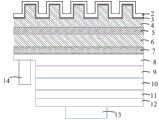
图1~11为本发明一具体实施方式中图形化Si衬底的LED器件制备方法工艺流程图,其中:1 to 11 are process flow diagrams of a method for fabricating an LED device with a patterned Si substrate in a specific embodiment of the present invention, wherein:
图1为Si(111)衬底示意图;Fig. 1 is the schematic diagram of Si (111) substrate;
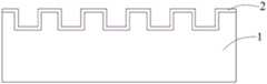
图2为在Si(111)衬底上制作图形化Si衬底的示意图;Fig. 2 is the schematic diagram of making patterned Si substrate on Si (111) substrate;
图3为在图形化Si衬底上生长Al2O3涂层步骤的示意图;Fig. 3 is the schematic diagram of growing Al2 O3 coating steps on patterned Si substrate;
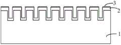
图4a和图4b为在Al2O3涂层上外延生长成核层的示意图;4a and 4b are schematic diagrams of epitaxial growth of a nucleation layer on an Al2 O3 coating;
图5a和图5b为在成核层上外延生长第一缓冲层的示意图;5a and 5b are schematic diagrams of epitaxially growing a first buffer layer on the nucleation layer;
图6为在第一缓冲层上外延生长应力缓冲层的示意图;6 is a schematic diagram of epitaxially growing a stress buffer layer on the first buffer layer;
图7为在应力缓冲层上外延生长发光结构的示意图;7 is a schematic diagram of epitaxially growing a light-emitting structure on a stress buffer layer;
图8为在发光结构上沉积焊接面金属层的示意图;8 is a schematic diagram of depositing a metal layer on a welding surface on a light-emitting structure;
图9为通过焊接镜面金属层将LED外延片转移到Si(100)基板上的示意图;9 is a schematic diagram of transferring an LED epitaxial wafer to a Si(100) substrate by welding a mirror metal layer;
图10为在Si(100)基板上制作欧姆接触p电极,在n-GaN层上制作欧姆接触n电极的示意图;10 is a schematic diagram of making an ohmic contact p-electrode on a Si(100) substrate and making an ohmic contact n-electrode on an n-GaN layer;
图11为用去除图形化Si衬底的示意图。Figure 11 is a schematic diagram of a patterned Si substrate with removal.
具体实施方式Detailed ways
以下将结合附图所示的具体实施方式对本发明进行详细描述。但这些实施方式并不限制本发明,本领域的普通技术人员根据这些实施方式所做出的结构、方法、或功能上的变换均包含在本发明的保护范围内。The present invention will be described in detail below with reference to the specific embodiments shown in the accompanying drawings. However, these embodiments do not limit the present invention, and structural, method, or functional changes made by those skilled in the art according to these embodiments are all included in the protection scope of the present invention.
参照图1~图11所示,本实施方式中基于图形化Si衬底的LED外延片的制备方法具体包括以下步骤:Referring to FIGS. 1 to 11 , the method for preparing an LED epitaxial wafer based on a patterned Si substrate in this embodiment specifically includes the following steps:
(1)、准备平板Si衬底(如图1所示),先在平板Si衬底(参图1所示) 上刻蚀图形化结构,制备出图形化Si衬底1(Patterned silicon substrate,PSS)。本案较佳地可以选择用干法刻蚀法刻蚀图形化结构。(1), prepare a flat Si substrate (as shown in Figure 1), first etch the patterned structure on the flat Si substrate (as shown in Figure 1), and prepare a patterned Si substrate 1 (Patterned silicon substrate, PSS). In this case, the patterned structure may preferably be etched by dry etching.
所述Si衬底为Si(111)晶面或Si(100)晶面或Si(110)晶面,掺杂类型为 n型或p型。The Si substrate is Si(111) crystal plane, Si(100) crystal plane or Si(110) crystal plane, and the doping type is n-type or p-type.
本案对在Si衬底刻蚀的图形化结构不作特别限制,可根据设计需求制作相应的图形化结构,In this case, the patterned structure etched on the Si substrate is not particularly limited, and the corresponding patterned structure can be fabricated according to the design requirements.
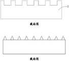
参照图2所示的截面图和俯视图,可以在硅衬底制作的图形化结构很丰富,这里只列举一些常做的图形化结构,然而本案不以此为限。Referring to the cross-sectional view and the top view shown in FIG. 2 , there are many patterned structures that can be fabricated on a silicon substrate. Here, only some commonly made patterned structures are listed, but this case is not limited to this.
图形化Si衬底一方面可以有效减少GaN外延材料中的位错密度,提高外延层晶体质量,从而减小有源区的非辐射复合,减小反向漏电流,提高LED 的寿命;另一方面有源区发出的光,经GaN和Al2O3涂层界面多次散射,改变了全反射光的出射角,增加了倒装LED的光从Al2O3涂层出射的几率,从而提高了光的提取效率。On the one hand, the patterned Si substrate can effectively reduce the dislocation density in the GaN epitaxial material and improve the crystal quality of the epitaxial layer, thereby reducing the non-radiative recombination of the active area, reducing the reverse leakage current and improving the life of the LED; On the other hand, the light emitted from the active area is scattered multiple times by the interface between the GaN and Al2 O3 coating, which changes the exit angle of the total reflection light, and increases the probability of the light of the flip-chip LED exiting from the Al2 O3 coating. The light extraction efficiency is improved.
(2)、参照图3所示,采用分子束外延生长法(MBE)生长Al2O3涂层,具体是:在图形化Si衬底1上先镀上一层厚度为1~200nm的Al层,再通入氧等离子体形成Al2O3涂层。(2) Referring to FIG. 3 , use molecular beam epitaxy (MBE) to grow the Al2 O3 coating, specifically: firstly coat a layer of Al with a thickness of 1-200 nm on the
为了避免回熔反应,在Si衬底上制备的LED器件结构必须先生长AlN 作为成核层,再在其上生长GaN外延层,但是AlN生长模式倾向于柱状生长模式,在没有Al2O3涂层的图形化Si衬底上生长时会产生AlN晶壁的问题,导致其上的GaN层产生间隙或者需较厚的GaN层才能完全合并;而且AlN 成核层可以在任意的晶面上生长,用AlN作为成核层甚至可能制成多晶的外延膜。而若以Al2O3作为涂层就能有效的保护Si衬底,避免了回熔反应,可直接采用GaN成核层实现单晶生长。GaN的生长速度是在(0002)方向最快,其他方向的生长速度会受到(0002)方向生长的抑制,从而解决GaN晶粒之间不能有效合并的问题。以此可以制备出大尺寸Si衬底GaN基LED外延片,为发展大功率Si衬底GaN基LED器件和降低LED价格提供了保证。In order to avoid the reflow reaction, the LED device structure prepared on the Si substrate must first grow AlN as the nucleation layer, and then grow the GaN epitaxial layer on it, but the AlN growth mode tends to the columnar growth mode, in the absence of Al2 O3 The AlN crystal wall problem occurs when the coating is grown on the patterned Si substrate, resulting in gaps in the GaN layer on it or requiring a thicker GaN layer to fully merge; and the AlN nucleation layer can be on any crystal plane. It is even possible to make polycrystalline epitaxial films using AlN as a nucleation layer. However, if Al2 O3 is used as the coating, the Si substrate can be effectively protected, the melting back reaction can be avoided, and the single crystal growth can be realized directly by using the GaN nucleation layer. The growth rate of GaN is the fastest in the (0002) direction, and the growth rate in other directions will be inhibited by the growth in the (0002) direction, so as to solve the problem that the GaN grains cannot be effectively merged. In this way, a large-size Si-substrate GaN-based LED epitaxial wafer can be prepared, which provides a guarantee for developing high-power Si-substrate GaN-based LED devices and reducing LED prices.
(3)、参照图4a和4b所示,在Al2O3涂层上生长出一层成核层3。图4a 所示的是:当Si衬底上的图形化结构的凹槽的宽度较大时,其凹槽的内壁和底部都可以生长成核层3。但是,如果当Si衬底上的图形化结构的凹槽的宽度较小时,以致原子无法进入时,则如图4b所示,无法在凹槽的内壁和底部生长成核层3。(3) Referring to Figures 4a and 4b, a
本案中,成核层3较佳的可为AlGaN或GaN。In this case, the
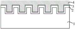
(4)、参照图5a和5b所示,在成核层3上通过MOCVD方法外延生长出一层厚度在100~5000nm的第一缓冲层4。第一缓冲层4较佳得为GaN。(4) Referring to Figures 5a and 5b, a first buffer layer 4 with a thickness of 100-5000 nm is epitaxially grown on the
图5a对应图4a,当图形化的结构的凹槽较宽时,第一缓冲层4可以生长到凹槽的侧壁和底部。FIG. 5a corresponds to FIG. 4a. When the groove of the patterned structure is wider, the first buffer layer 4 can be grown to the sidewall and bottom of the groove.
图5b对应图4b,当图形化的结构的凹槽较窄时,第一GaN缓冲层4无法生长到凹槽的侧壁和底部,且紧靠凹槽口的部分也无法生长第一GaN缓冲层4。FIG. 5b corresponds to FIG. 4b. When the groove of the patterned structure is narrow, the first GaN buffer layer 4 cannot grow to the sidewalls and bottom of the groove, and the first GaN buffer cannot grow on the part close to the groove opening. Layer 4.
(5)参照图6所示,在第一GaN缓冲层4上通过MOCVD方法外延生长应力缓冲层。应力缓冲层可以起到调节应力的作用。(5) Referring to FIG. 6 , a stress buffer layer is epitaxially grown on the first GaN buffer layer 4 by the MOCVD method. The stress buffer layer can play the role of adjusting the stress.
本案中,较佳地,应力缓冲层由第一插入层5、第二缓冲层6及第二插入层7组成。但是本案并不以此为限,应力缓冲层也可以由3个插入层和2个缓冲层交替组成,或者更多个插入层和更多个缓冲层交替组成的。In this case, preferably, the stress buffer layer is composed of a
本案中,较佳地,第一插入层5和第二插入层7可为AlGaN插入层、AlN 插入层或者超晶格插入层中的任一种。In this case, preferably, the
第一插入层5和第二插入层7的厚度为5-100nm,第二缓冲层6的厚度为 100-5000nm。The thickness of the
(6)参照图7所示,在应力缓冲层上通过MOVCD方法外延生长出发光结构层。本案中,较佳地,发光结构层为1~5μm的n-GaN层8、多层结构的量子阱层9、0.1~2μm的P-GaN层10。(6) Referring to FIG. 7 , a light emitting structure layer is epitaxially grown on the stress buffer layer by the MOVCD method. In this case, preferably, the light-emitting structure layer is an n-
(7)参照图8所示,通过溅射、金属蒸发或电镀的方法在p-GaN层上覆设一层焊接镜面金属层11,此层为镀银或镁的铝板或镍板,铝板或镍板与 p-GaN层粘接形成欧姆接触。(7) Referring to FIG. 8, a welding
(8)参照图9所示,将此外延层通过焊接金属层转移到新的低阻双面抛光Si基板12上,并采用倒装芯片工艺,以焊接镜面金属层11反光,从Al2O3涂层出光。(8) Referring to FIG. 9 , transfer the epitaxial layer to a new low-resistance double-sided
(9)参照图10所示,在Si基板12上制作欧姆接触的p电极13。(9) Referring to FIG. 10 , the p-
采用干法刻蚀方法从Si基板12开始刻蚀,直至露出n-GaN层8,并在暴露的n-GaN层8上镀透明电极,在透明电极上溅射金或镍并刻蚀成电极图案,形成欧姆接触的n电极14。The dry etching method is used to start etching from the
(10)参照图11所示,利用Al2O3涂层作为阻挡层,用湿法刻蚀的方法把图形化Si衬底1去掉,露出图形化的Al2O3涂层,形成LED器件。(10) Referring to FIG. 11, using the Al2 O3 coating as a barrier layer, the
与现有技术相比,本发明的有益效果是:Compared with the prior art, the beneficial effects of the present invention are:
1、本发明采用的是图形化硅衬底,图形化硅衬底与目前LED产业中使用的图形化蓝宝石衬底相比更容易在Si衬底上制作出各类图形,而且图形的大小和样式选择也较蓝宝石衬底更多;此外,图形化Si衬底还有如下优点:一方面可以有效减少GaN外延材料的位错密度,从而减小有源区的非辐射复合,减小反向漏电流,提高LED的寿命;另一方面有源区发出的光,经GaN 和衬底界面多次散射,改变了全反射光的出射角,增加了倒装LED的光从衬底出射的几率,从而提高了光的提取效率。1. The present invention adopts a patterned silicon substrate. Compared with the patterned sapphire substrate currently used in the LED industry, the patterned silicon substrate is easier to produce various patterns on the Si substrate. There are also more choices of styles than the sapphire substrate; in addition, the patterned Si substrate has the following advantages: on the one hand, it can effectively reduce the dislocation density of the GaN epitaxial material, thereby reducing the non-radiative recombination of the active area and reducing the reverse On the other hand, the light emitted from the active area is scattered multiple times by the interface between the GaN and the substrate, which changes the exit angle of the total reflection light and increases the probability of the light from the flip-chip LED exiting from the substrate. , thereby improving the light extraction efficiency.
2、本发明采用在图形化硅衬底上生长Al2O3涂层,然后直接生长GaN或 AlGaN成核层,传统Si衬底上的LED器件结构需要先生长AlN作为成核层,再在其上生长GaN外延层,但是AlN生长模式倾向于柱状生长模式,在PSS 衬底上生长时会产生AlN晶壁的问题,导致其上的GaN层产生间隙或者需较厚的GaN层才能完全合并,若以GaN或AlGaN作为成核层就能解决GaN晶粒之间不能有效合并的问题。以此可以制备出大尺寸Si衬底GaN基LED外延片,为发展大功率Si衬底GaN基LED器件和降低LED价格提供了保证。2. In the present invention, Al2 O3 coating is grown on the patterned silicon substrate, and then the GaN or AlGaN nucleation layer is grown directly. The LED device structure on the traditional Si substrate needs to grow AlN as the nucleation layer first, and then grow the nucleation layer on the traditional Si substrate. The GaN epitaxial layer is grown on it, but the AlN growth mode tends to the columnar growth mode, and the AlN crystal wall problem will occur when growing on the PSS substrate, resulting in gaps in the GaN layer on it or requiring a thicker GaN layer to be fully merged , if GaN or AlGaN is used as the nucleation layer, the problem that GaN grains cannot be effectively merged can be solved. In this way, a large-size Si-substrate GaN-based LED epitaxial wafer can be prepared, which provides a guarantee for developing high-power Si-substrate GaN-based LED devices and reducing LED prices.
3、在整个LED器件结构中加入应力缓冲层,解决了由于GaN外延层在降温时受到Si衬底带来的张应力引起的外延层表面龟裂问题。3. Adding a stress buffer layer to the entire LED device structure solves the problem of surface cracking of the epitaxial layer caused by the tensile stress brought by the Si substrate when the GaN epitaxial layer is cooled.
对于本领域技术人员而言,显然本发明不限于上述示范性实施例的细节,而且在不背离本发明的精神或基本特征的情况下,能够以其他的具体形式实现本发明。因此,无论从哪一点来看,均应将实施例看作是示范性的,而且是非限制性的,本发明的范围由所附权利要求而不是上述说明限定,因此旨在将落在权利要求的等同要件的含义和范围内的所有变化囊括在本发明内。不应将权利要求中的任何附图标记视为限制所涉及的权利要求。It will be apparent to those skilled in the art that the present invention is not limited to the details of the above-described exemplary embodiments, but that the present invention may be embodied in other specific forms without departing from the spirit or essential characteristics of the invention. Therefore, the embodiments are to be regarded in all respects as illustrative and not restrictive, and the scope of the invention is to be defined by the appended claims rather than the foregoing description, which are therefore intended to fall within the scope of the claims. All changes within the meaning and scope of the equivalents of , are included in the present invention. Any reference signs in the claims shall not be construed as limiting the involved claim.
此外,应当理解,虽然本说明书按照实施方式加以描述,但并非每个实施方式仅包含一个独立的技术方案,说明书的这种叙述方式仅仅是为清楚起见,本领域技术人员应当将说明书作为一个整体,各实施例中的技术方案也可以经适当组合,形成本领域技术人员可以理解的其他实施方式。In addition, it should be understood that although this specification is described in terms of embodiments, not each embodiment only includes an independent technical solution, and this description in the specification is only for the sake of clarity, and those skilled in the art should take the specification as a whole , the technical solutions in each embodiment can also be appropriately combined to form other implementations that can be understood by those skilled in the art.
Claims (5)
Priority Applications (4)
| Application Number | Priority Date | Filing Date | Title |
|---|---|---|---|
| CN201610187818.8ACN105591004B (en) | 2016-03-29 | 2016-03-29 | LED epitaxial wafer based on patterned Si substrate and preparation method thereof |
| TW106108297ATWI751143B (en) | 2016-03-29 | 2017-03-14 | LED epitaxial wafer based on patterned Si substrate and preparation method thereof |
| US16/090,563US10964843B2 (en) | 2016-03-29 | 2017-03-28 | Patterned Si substrate-based LED epitaxial wafer and preparation method therefor |
| PCT/CN2017/078475WO2017167190A1 (en) | 2016-03-29 | 2017-03-28 | Graphical si substrate-based led epitaxial wafer and preparation method therefor |
Applications Claiming Priority (1)
| Application Number | Priority Date | Filing Date | Title |
|---|---|---|---|
| CN201610187818.8ACN105591004B (en) | 2016-03-29 | 2016-03-29 | LED epitaxial wafer based on patterned Si substrate and preparation method thereof |
Publications (2)
| Publication Number | Publication Date |
|---|---|
| CN105591004A CN105591004A (en) | 2016-05-18 |
| CN105591004Btrue CN105591004B (en) | 2020-07-10 |
Family
ID=55930434
Family Applications (1)
| Application Number | Title | Priority Date | Filing Date |
|---|---|---|---|
| CN201610187818.8AActiveCN105591004B (en) | 2016-03-29 | 2016-03-29 | LED epitaxial wafer based on patterned Si substrate and preparation method thereof |
Country Status (4)
| Country | Link |
|---|---|
| US (1) | US10964843B2 (en) |
| CN (1) | CN105591004B (en) |
| TW (1) | TWI751143B (en) |
| WO (1) | WO2017167190A1 (en) |
Families Citing this family (16)
| Publication number | Priority date | Publication date | Assignee | Title |
|---|---|---|---|---|
| CN105591004B (en)* | 2016-03-29 | 2020-07-10 | 苏州晶湛半导体有限公司 | LED epitaxial wafer based on patterned Si substrate and preparation method thereof |
| WO2018161300A1 (en)* | 2017-03-09 | 2018-09-13 | Enkris Semiconductor, Inc | Stripped method for prepairing semiconductor structure |
| US20190198709A1 (en) | 2017-12-22 | 2019-06-27 | Lumileds Llc | Iii-nitride multi-color on wafer micro-led enabled by tunnel junctions |
| CN110556454B (en)* | 2018-06-01 | 2021-08-03 | 上海新微技术研发中心有限公司 | Nitride epitaxial structure grown on silicon base substrate and its growth method |
| CN109599468B (en)* | 2018-11-20 | 2020-09-11 | 华中科技大学鄂州工业技术研究院 | Ultra-wide band gap aluminum nitride material epitaxial wafer and preparation method thereof |
| CN110190163B (en)* | 2019-05-24 | 2020-04-28 | 康佳集团股份有限公司 | Patterned substrate, epitaxial wafer, manufacturing method, storage medium and LED chip |
| CN112701197A (en)* | 2019-10-22 | 2021-04-23 | 东莞市中图半导体科技有限公司 | Graphical composite substrate, preparation method and LED epitaxial wafer |
| US11264530B2 (en) | 2019-12-19 | 2022-03-01 | Lumileds Llc | Light emitting diode (LED) devices with nucleation layer |
| US11211527B2 (en) | 2019-12-19 | 2021-12-28 | Lumileds Llc | Light emitting diode (LED) devices with high density textures |
| US12408481B2 (en) | 2019-12-19 | 2025-09-02 | Lumileds Llc | Light emitting diode (LED) devices with nucleation layer |
| CN113113518B (en)* | 2021-02-24 | 2022-05-13 | 华灿光电(苏州)有限公司 | Light emitting diode epitaxial wafer and preparation method thereof |
| CN114420537B (en)* | 2021-12-29 | 2025-10-03 | 上海至纯洁净系统科技股份有限公司 | Epitaxial wafer manufacturing method for reducing internal stress of power devices and epitaxial wafer |
| CN117410415A (en)* | 2022-06-30 | 2024-01-16 | 苏州晶湛半导体有限公司 | Composite substrate and manufacturing method thereof, semiconductor device |
| CN116344698B (en)* | 2023-05-22 | 2023-08-29 | 江西兆驰半导体有限公司 | Patterned substrate GaN-based LED epitaxial wafer and preparation method thereof |
| EP4539100A1 (en)* | 2023-10-12 | 2025-04-16 | Siltronic AG | Semiconductor wafer having a multilayered structure and method for producing the same |
| CN117832352A (en)* | 2023-12-29 | 2024-04-05 | 福建晶安光电有限公司 | Patterned substrate, epitaxial wafer and preparation method, flip-chip light-emitting diode |
Citations (3)
| Publication number | Priority date | Publication date | Assignee | Title |
|---|---|---|---|---|
| CN101145516A (en)* | 2007-09-29 | 2008-03-19 | 中国电子科技集团公司第五十五研究所 | Epitaxial structure and growth method of silicon-based nitride single crystal thin film |
| CN103035794A (en)* | 2012-12-11 | 2013-04-10 | 广州市众拓光电科技有限公司 | Light-emitting diode (LED) epitaxial wafer developed on silicon (Si) substrate and preparation method thereof |
| CN203910840U (en)* | 2014-06-10 | 2014-10-29 | 广州市众拓光电科技有限公司 | LED epitaxial wafer grown on Si patterned substrate |
Family Cites Families (17)
| Publication number | Priority date | Publication date | Assignee | Title |
|---|---|---|---|---|
| JP3809464B2 (en) | 1999-12-14 | 2006-08-16 | 独立行政法人理化学研究所 | Method for forming semiconductor layer |
| TWI260800B (en)* | 2005-05-12 | 2006-08-21 | Epitech Technology Corp | Structure of light-emitting diode and manufacturing method thereof |
| CN1881624A (en)* | 2005-06-15 | 2006-12-20 | 上海蓝光科技有限公司 | Light-emitting diode and its preparation method |
| US7956370B2 (en)* | 2007-06-12 | 2011-06-07 | Siphoton, Inc. | Silicon based solid state lighting |
| CN101471402A (en)* | 2007-12-27 | 2009-07-01 | 深圳市方大国科光电技术有限公司 | Method for preparing graphical substrate of GaN-based LED by silicon 001 crystal face |
| CN101728244A (en) | 2008-10-21 | 2010-06-09 | 先进开发光电股份有限公司 | Method for blocking dislocation defect of semiconductor |
| CN101555587A (en)* | 2009-05-13 | 2009-10-14 | 长春理工大学 | Magnetron sputtering preparation method of Mg*Zn1***O thin film of silicon substrate with Al*O* buffer layer |
| CN101599466B (en)* | 2009-07-10 | 2012-08-29 | 中山大学 | Graphic substrate for epitaxial growth and production method thereof |
| CN201766093U (en)* | 2010-05-18 | 2011-03-16 | 上海蓝宝光电材料有限公司 | Gallium nitride light-emitting diode |
| CN102130223B (en)* | 2010-12-06 | 2012-07-25 | 山东华光光电子有限公司 | Method for coarsening surface of GaN-based LED epitaxial wafer |
| US8507947B2 (en) | 2011-12-09 | 2013-08-13 | Power Integrations, Inc. | High quality GaN high-voltage HFETS on silicon |
| CN102723416A (en)* | 2012-07-05 | 2012-10-10 | 杭州士兰明芯科技有限公司 | LED epitaxial wafer and manufacturing method thereof |
| CN103035496B (en)* | 2012-12-11 | 2016-03-23 | 广州市众拓光电科技有限公司 | A kind of growth GaN film on a si substrate and its preparation method and application |
| KR20140121192A (en)* | 2013-04-05 | 2014-10-15 | 삼성전자주식회사 | Substrate structure and semiconductor device employing the same |
| CN105393336B (en)* | 2013-07-22 | 2017-10-31 | 日本碍子株式会社 | Composite substrate, manufacturing method thereof, functional element, and seed crystal substrate |
| CN104593727B (en)* | 2014-12-24 | 2017-08-29 | 西安神光安瑞光电科技有限公司 | A kind of method that utilization AAO templates prepare nano-patterned substrate |
| CN105591004B (en) | 2016-03-29 | 2020-07-10 | 苏州晶湛半导体有限公司 | LED epitaxial wafer based on patterned Si substrate and preparation method thereof |
- 2016
- 2016-03-29CNCN201610187818.8Apatent/CN105591004B/enactiveActive
- 2017
- 2017-03-14TWTW106108297Apatent/TWI751143B/enactive
- 2017-03-28WOPCT/CN2017/078475patent/WO2017167190A1/ennot_activeCeased
- 2017-03-28USUS16/090,563patent/US10964843B2/enactiveActive
Patent Citations (3)
| Publication number | Priority date | Publication date | Assignee | Title |
|---|---|---|---|---|
| CN101145516A (en)* | 2007-09-29 | 2008-03-19 | 中国电子科技集团公司第五十五研究所 | Epitaxial structure and growth method of silicon-based nitride single crystal thin film |
| CN103035794A (en)* | 2012-12-11 | 2013-04-10 | 广州市众拓光电科技有限公司 | Light-emitting diode (LED) epitaxial wafer developed on silicon (Si) substrate and preparation method thereof |
| CN203910840U (en)* | 2014-06-10 | 2014-10-29 | 广州市众拓光电科技有限公司 | LED epitaxial wafer grown on Si patterned substrate |
Also Published As
| Publication number | Publication date |
|---|---|
| WO2017167190A1 (en) | 2017-10-05 |
| US20190148586A1 (en) | 2019-05-16 |
| CN105591004A (en) | 2016-05-18 |
| US10964843B2 (en) | 2021-03-30 |
| TWI751143B (en) | 2022-01-01 |
| TW201735400A (en) | 2017-10-01 |
Similar Documents
| Publication | Publication Date | Title |
|---|---|---|
| CN105591004B (en) | LED epitaxial wafer based on patterned Si substrate and preparation method thereof | |
| US7687376B2 (en) | Method of manufacturing vertical gallium nitride-based light emitting diode | |
| US8735185B2 (en) | Light emitting device and fabrication method thereof | |
| CN111628058A (en) | AlGaInP-based light emitting diode chip and manufacturing method thereof | |
| CN107112394B (en) | Light emitting diode and light emitting diode array comprising the same | |
| TWI422068B (en) | Roughening method and preparation method of light-emitting diode with roughened surface | |
| TW201706452A (en) | Method for stripping growth substrate by chemical etching | |
| CN102598270A (en) | High brightness light emitting diode covered by zinc oxide layers on multiple surfaces grown in low temperature aqueous solution | |
| CN1964090B (en) | Nitride-based semiconductor device and manufacturing method thereof | |
| CN112018223A (en) | Thin film flip structure Micro-LED chip with transfer printing of bonding layer and preparation method thereof | |
| JP2012243815A (en) | Semiconductor light-emitting device, wafer, and method of manufacturing nitride semiconductor crystal layer | |
| CN101826579A (en) | Light emitting device | |
| JP5237780B2 (en) | Manufacturing method of semiconductor light emitting device | |
| JP2010219310A (en) | Optical device and optical device structure | |
| JP5638543B2 (en) | Method for manufacturing light emitting device | |
| CN110034216A (en) | III-V nitride deep-UV light-emitting diode structure and preparation method thereof | |
| CN107958900A (en) | A kind of light emitting diode of vertical stratification | |
| JP5379703B2 (en) | Ultraviolet semiconductor light emitting device | |
| CN118299485A (en) | Red light LED chip preparation method and red light LED chip | |
| KR101068864B1 (en) | Semiconductor light emitting device and manufacturing method thereof | |
| CN111968907A (en) | Nitrogen polarity III group nitride coarsening method | |
| KR101154321B1 (en) | Light emitting diode and method of fabricating the same | |
| KR101072199B1 (en) | Light emitting device and method for fabricating the same | |
| TW202322419A (en) | Vertical light emitting diode and its manufacturing method | |
| CN116472653A (en) | Preparation method of resonant cavity light-emitting diode |
Legal Events
| Date | Code | Title | Description |
|---|---|---|---|
| C06 | Publication | ||
| PB01 | Publication | ||
| C10 | Entry into substantive examination | ||
| SE01 | Entry into force of request for substantive examination | ||
| CB02 | Change of applicant information | Address after:215123, 517-A, room 20, building NW-20, northwest 99 Jinji Road, Suzhou Industrial Park, Jiangsu, China Applicant after:ENKRIS SEMICONDUCTOR, Inc. Address before:215124, 517-A, room 20, building NW-20, northwest 99 Jinji Road, Suzhou Industrial Park, Jiangsu, China Applicant before:ENKRIS SEMICONDUCTOR, Inc. | |
| COR | Change of bibliographic data | ||
| GR01 | Patent grant | ||
| GR01 | Patent grant | ||
| TR01 | Transfer of patent right | ||
| TR01 | Transfer of patent right | Effective date of registration:20230619 Address after:No. 108, Furong Middle Road, Xishan Economic and Technological Development Zone, Xishan District, Wuxi City, Jiangsu Province, 214000 Patentee after:Wuxi JingZhan Semiconductor Co.,Ltd. Address before:215123 room 517-a, building 20 (nw-20), Northwest District, No. 99, Jinjihu Avenue, Suzhou Industrial Park, Jiangsu Province Patentee before:ENKRIS SEMICONDUCTOR, Inc. |