CN105405785B - Silicon through hole test structure before binding based on arbiter - Google Patents
Silicon through hole test structure before binding based on arbiterDownload PDFInfo
- Publication number
- CN105405785B CN105405785BCN201510757342.2ACN201510757342ACN105405785BCN 105405785 BCN105405785 BCN 105405785BCN 201510757342 ACN201510757342 ACN 201510757342ACN 105405785 BCN105405785 BCN 105405785B
- Authority
- CN
- China
- Prior art keywords
- inverter
- tsv
- fault
- capacitor
- arbiter
- Prior art date
- Legal status (The legal status is an assumption and is not a legal conclusion. Google has not performed a legal analysis and makes no representation as to the accuracy of the status listed.)
- Expired - Fee Related
Links
Images


Classifications
- H—ELECTRICITY
- H01—ELECTRIC ELEMENTS
- H01L—SEMICONDUCTOR DEVICES NOT COVERED BY CLASS H10
- H01L22/00—Testing or measuring during manufacture or treatment; Reliability measurements, i.e. testing of parts without further processing to modify the parts as such; Structural arrangements therefor
- H01L22/30—Structural arrangements specially adapted for testing or measuring during manufacture or treatment, or specially adapted for reliability measurements
- H01L22/34—Circuits for electrically characterising or monitoring manufacturing processes, e. g. whole test die, wafers filled with test structures, on-board-devices incorporated on each die, process control monitors or pad structures thereof, devices in scribe line
Landscapes
- Engineering & Computer Science (AREA)
- Manufacturing & Machinery (AREA)
- Automation & Control Theory (AREA)
- Computer Hardware Design (AREA)
- Microelectronics & Electronic Packaging (AREA)
- Power Engineering (AREA)
- Tests Of Electronic Circuits (AREA)
Abstract
Translated fromChinese
Description
Translated fromChinese技术领域technical field
本发明涉及超大规模集成电路测试技术领域,具体是一种基于仲裁器的绑定前硅通孔测试结构。The invention relates to the technical field of ultra-large-scale integrated circuit testing, in particular to an arbiter-based through-silicon via test structure before binding.
背景技术Background technique
基于硅通孔(Through-Silicon Via,TSV)的三维集成电路极大地推动了集成电路行业的发展。与传统的二维集成电路不同,三维集成电路通过TSV把多个晶片垂直堆叠,使得它拥有功耗低、带宽高、面积小、性能好、支持异构集成等优点。据估计,基于TSV垂直互连的三维集成电路功耗降低50%,带宽提高8倍,堆叠存储器缩小35%。Three-dimensional integrated circuits based on through-silicon vias (TSVs) have greatly promoted the development of the integrated circuit industry. Different from traditional two-dimensional integrated circuits, three-dimensional integrated circuits stack multiple wafers vertically through TSV, which makes it have the advantages of low power consumption, high bandwidth, small area, good performance, and support for heterogeneous integration. It is estimated that the power consumption of 3D integrated circuits based on TSV vertical interconnection is reduced by 50%, the bandwidth is increased by 8 times, and the stacked memory is reduced by 35%.
当前TSV的制造工艺还不成熟,TSV可能存在微孔和针孔缺陷,这些缺陷导致TSV产生电阻开路故障和泄漏故障,严重降低了三维集成电路的良率和可靠性,因此三维集成电路的TSV测试非常必要。近期国内外许多著名研究结构和学者的学术研究都涉及了三维集成电路TSV的测试,如绑定前TSV测试、绑定后TSV测试等。绑定前测试主要检测TSV是否存在制造缺陷,绑定后测试则检测TSV在绑定过程中是否引入新的缺陷。绑定前阶段晶片未薄化时,TSV底端埋于衬底中限制了TSV的可观察性;在晶片薄化后,虽然TSV底端露出可以访问,但由于测试探针的最小间距远大于TSV的间距,使用探针测试TSV非常困难,绑定前测试仍面临着巨大的挑战。此外,在绑定前阶段检测出故障TSV能够明显增加三维集成电路堆叠的良率,因此绑定前进行TSV测试尤为重要。At present, the manufacturing process of TSV is immature, and TSV may have micro-hole and pin-hole defects. These defects cause TSV to produce resistance open circuit failure and leakage failure, which seriously reduces the yield and reliability of 3D integrated circuits. Therefore, the TSV of 3D integrated circuits Testing is necessary. Recently, many well-known research structures and academic research by scholars at home and abroad have involved the testing of 3D integrated circuit TSVs, such as pre-binding TSV testing and post-binding TSV testing. The pre-binding test mainly detects whether the TSV has manufacturing defects, and the post-binding test detects whether the TSV introduces new defects during the binding process. When the wafer is not thinned in the pre-bonding stage, the bottom of the TSV is buried in the substrate, which limits the observability of the TSV. Spacing of TSVs, testing TSVs with probes is very difficult, and pre-bonding testing still faces huge challenges. In addition, the detection of faulty TSVs in the pre-bonding stage can significantly increase the yield of 3D IC stacks, so it is particularly important to perform TSV testing before bonding.
采用PMOS管漏电流的方法可以检测TSV的泄漏故障,通过检测发生泄漏故障的泄漏电阻大小来判断TSV是否存在泄漏故障。采用电桥电路的方法可以检测TSV的完全开路故障,比较被测TSV与无故障TSV电容大小来判断TSV是否存在完全开路故障。这类方法只能够检测单类故障且可检测故障范围有限,严重降低了整体三维集成电路的良率。The leakage fault of the TSV can be detected by using the method of the leakage current of the PMOS tube, and the leakage fault of the TSV can be judged by detecting the leakage resistance of the leakage fault. The bridge circuit method can be used to detect the complete open circuit fault of the TSV, and compare the capacitance of the tested TSV with that of the non-faulty TSV to determine whether the TSV has a complete open circuit fault. Such methods can only detect a single type of fault and have a limited range of detectable faults, which seriously reduces the yield of the overall 3D integrated circuit.
基于环形振荡器的方法可以检测出TSV的单种电阻开路故障和单种泄漏故障。该方法把TSV作为环形振荡器的负载,通过比较被测TSV的环形振荡器振荡周期与无故障TSV振荡周期来判断TSV是否存在故障。然而该种方法有以下问题:1)测试精度较低,并且能检测的故障范围有限。2)当一个TSV同时存在电阻开路故障和泄漏故障时,两种故障对于环形振荡器振荡周期有着相反的影响,会使得故障效应相互抵消从而导致误测。The ring oscillator-based method can detect single-type open-resistance faults and single-type leakage faults of TSV. In this method, the TSV is used as the load of the ring oscillator, and whether the TSV is faulty is judged by comparing the oscillation period of the ring oscillator of the tested TSV with the oscillation period of the non-faulty TSV. However, this method has the following problems: 1) The test accuracy is low, and the range of faults that can be detected is limited. 2) When a TSV has both an open resistance fault and a leakage fault, the two faults have opposite effects on the oscillation period of the ring oscillator, which will cancel each other out and cause false detection.
发明内容 本发明的目的是提供一种基于仲裁器的绑定前硅通孔测试结构,以克服现有TSV测试方案中存在的不足,该硅通孔测试结构可以检测电阻开路故障、泄漏故障以及两种故障共存情况下的TSV,测试精度高且可检测故障范围广,并且提供TSV故障严重程度分级的功能。SUMMARY OF THE INVENTION The object of the present invention is to provide an arbiter-based pre-bonding TSV test structure to overcome the deficiencies in the existing TSV test solutions, the TSV test structure can detect open resistance faults, leakage faults and The TSV under the coexistence of two faults has high test accuracy and can detect a wide range of faults, and provides the function of grading the severity of TSV faults.
为了达到上述目的,本发明所采用的技术方案为:In order to achieve the above object, the technical scheme adopted in the present invention is:
一种基于仲裁器的绑定前硅通孔测试结构,其特征在于:包括参考延时电路、被测TSV模块电路、仲裁器电路、输入节点In、输出节点Out1、输出节点Out2,其中:An arbiter-based through-silicon via test structure before binding, characterized in that it includes a reference delay circuit, a TSV module circuit under test, an arbiter circuit, an input node In, an output node Out1, and an output node Out2, wherein:
所述参考延时电路由第一反相器、第二反相器、第三反相器、第四反相器、第一电容、第二电容、第三电容、第四电容、第一四选一多路选择器、第五反相器构成,其中第一反相器、第二反相器、第三反相器、第四反相器的输入端共接至输入节点In,第一反相器、第二反相器、第三反相器、第四反相的输出端一一对应与第一四选一多路选择器的四个输入端连接,且第一反相器、第二反相器、第三反相器、第四反相的输出端还一一对应通过第一电容、第二电容、第三电容、第四电容与地相连接,第一四选一多路选择器的输出端与第五反相器输入端连接,第五反相器输出端连接至仲裁器电路;The reference delay circuit consists of a first inverter, a second inverter, a third inverter, a fourth inverter, a first capacitor, a second capacitor, a third capacitor, a fourth capacitor, a first four A multiplexer and a fifth inverter are selected, wherein the input ends of the first inverter, the second inverter, the third inverter and the fourth inverter are connected to the input node In in common, and the first inverter, the second inverter, the third inverter and the fourth inverter are connected to the input node In. The output terminals of the inverter, the second inverter, the third inverter and the fourth inverter are connected to the four input terminals of the first four-to-one multiplexer in one-to-one correspondence, and the first inverter, The output terminals of the second inverter, the third inverter and the fourth inverter are also connected to the ground through the first capacitor, the second capacitor, the third capacitor and the fourth capacitor in one-to-one correspondence. The output end of the way selector is connected to the input end of the fifth inverter, and the output end of the fifth inverter is connected to the arbiter circuit;
所述被测TSV模块电路由第六反相器、被测TSV、第二四选一多路选择器、第七反相器构成,其中第六反相器的输入端连接至输入节点In,第六反相器的输出端分别连接至被测TSV、第二四选一多路选择器的四个输入端,第二四选一多路选择器的输出端与第七反相器的输入端连接,第七反相器的输出端连接至仲裁器电路;The TSV module circuit under test is composed of a sixth inverter, a TSV under test, a second four-to-one multiplexer, and a seventh inverter, wherein the input end of the sixth inverter is connected to the input node In, The output terminal of the sixth inverter is respectively connected to the TSV under test, the four input terminals of the second four-to-one multiplexer, the output terminal of the second four-to-one multiplexer and the input of the seventh inverter terminal is connected, and the output terminal of the seventh inverter is connected to the arbiter circuit;
所述仲裁器电路由第一与非门、第二与非门、第一PMOS管、第一NMOS管、第二PMOS管、第二NMOS管构成,所述参考延时电路中第五反相器输出端与第一与非门的输入端a相连接,被测TSV模块电路中第七反相器的输出端与第二与非门的输入端b相连接,第一与非门的输出端分别与第二与非门的输入端a、第一PMOS管的栅极、第一NMOS管的栅极、第二PMOS管的源极连接,第二与非门的输出端分别与第一与非门的输入端b、第二PMOS管的栅极、第二NMOS管的栅极、第一PMOS管的源极连接,第一PMOS管的漏极与第一NMOS管的漏极共接至输出节点Out1,第二PMOS管的漏极与第二NMOS管的漏极共接至输出节点Out2,第一NMOS管的源极、第二NMOS管的源极分别与地相连接。The arbiter circuit is composed of a first NAND gate, a second NAND gate, a first PMOS transistor, a first NMOS transistor, a second PMOS transistor, and a second NMOS transistor. In the reference delay circuit, the fifth phase is inverted. The output terminal of the inverter is connected to the input terminal a of the first NAND gate, the output terminal of the seventh inverter in the TSV module circuit under test is connected to the input terminal b of the second NAND gate, and the output terminal of the first NAND gate is connected. The terminals are respectively connected with the input terminal a of the second NAND gate, the gate of the first PMOS tube, the gate of the first NMOS tube, and the source of the second PMOS tube, and the output terminals of the second NAND gate are respectively connected with the first The input terminal b of the NAND gate, the gate of the second PMOS transistor, the gate of the second NMOS transistor, and the source of the first PMOS transistor are connected, and the drain of the first PMOS transistor is connected to the drain of the first NMOS transistor. To the output node Out1, the drain of the second PMOS transistor and the drain of the second NMOS transistor are connected to the output node Out2 in common, and the source of the first NMOS transistor and the source of the second NMOS transistor are respectively connected to ground.
所述的一种基于仲裁器的绑定前硅通孔测试结构,其特征在于:设无故障的TSV的等效电容为C,参考延时电路中的第一电容、第二电容、第三电容、第四电容的容值分别为略小于C的0.999C、0.995C、0.99C、0.9C。The pre-bonding TSV test structure based on an arbiter is characterized in that: setting the equivalent capacitance of a non-faulty TSV as C, and referring to the first capacitor, the second capacitor, the third capacitor in the delay circuit, and the The capacitance values of the capacitor and the fourth capacitor are 0.999C, 0.995C, 0.99C, and 0.9C, which are slightly smaller than C, respectively.
所述的一种基于仲裁器的绑定前硅通孔测试结构,其特征在于:所述第一反相器、第二反相器、第三反相器、第四反相器以及第六反相器的参数完全相同;第一四选一多路选择器与第二四选一多路选择器的参数完全相同;第五反相器与第七反相器的参数完全相同;第一与非门与第二与非门的参数完全相同;第一PMOS管与第二PMOS管的参数完全相同;第一NMOS管与第二NMOS管的参数完全相同。The pre-bonding TSV test structure based on an arbiter is characterized in that: the first inverter, the second inverter, the third inverter, the fourth inverter and the sixth inverter The parameters of the inverters are exactly the same; the parameters of the first four-to-one multiplexer and the second four-to-one multiplexer are exactly the same; the parameters of the fifth inverter and the seventh inverter are exactly the same; the first The parameters of the NAND gate and the second NAND gate are exactly the same; the parameters of the first PMOS transistor and the second PMOS transistor are exactly the same; the parameters of the first NMOS transistor and the second NMOS transistor are exactly the same.
本发明的有益效果为:The beneficial effects of the present invention are:
本发明利用发生故障TSV的延迟时间变小的原理,比较高电平信号通过被测TSV模块电路以及参考延时电路的延迟时间,在被测TSV模块延迟时间大于参考延时电路的延迟时间时认定该被测TSV无故障,否则该被测TSV存在故障;其延迟时间比较结果由仲裁器电路给出。被测TSV延迟时间与不同的参考延迟时间相比,可对其延迟进行区间定位,实现TSV故障分级。该发明能够有效的检测出电阻开路故障、泄漏故障以及两种故障共存的TSV;且具有测试精度高、可检测故障范围广等优点。The invention utilizes the principle that the delay time of the faulty TSV becomes smaller, and compares the delay time of the high-level signal passing through the TSV module circuit under test and the reference delay circuit. When the delay time of the TSV module under test is greater than the delay time of the reference delay circuit It is determined that the TSV under test has no fault, otherwise the TSV under test has a fault; the comparison result of its delay time is given by the arbiter circuit. The measured TSV delay time can be compared with different reference delay times, and its delay can be located in an interval to realize TSV fault classification. The invention can effectively detect resistance open circuit fault, leakage fault and TSV in which the two faults coexist; and has the advantages of high test accuracy, wide range of detectable faults, and the like.
附图说明Description of drawings
图1是最基本的基于仲裁器的绑定前硅通孔测试结构原理图。Figure 1 is a schematic diagram of the most basic arbiter-based pre-bond TSV test structure.
图2是本发明所述的基于仲裁器的绑定前硅通孔测试结构原理图。FIG. 2 is a schematic diagram of the pre-bonding TSV test structure based on the arbiter according to the present invention.
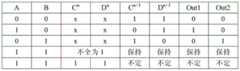
图3是仲裁器电路结构的真值表。FIG. 3 is a truth table of the circuit structure of the arbiter.
具体实施方式Detailed ways
发明一种基于仲裁器的绑定前硅通孔测试结构,包括参考延时电路、被测TSV模块电路、仲裁器电路、输入节点In、输出节点Out1和输出节点Out2;所述参考延时电路依次包括有第一反相器1、第二反相器2、第三反相器3、第四反相器4、第一电容5、第二电容6、第三电容7、第四电容8、第一四选一多路选择器9、第五反相器10;被测TSV模块电路依次包括第六反相器11、被测TSV12、第二四选一多路选择器13、第七反相器14;仲裁器电路依次包括第一与非门15、第二与非门16、第一PMOS管17、第一NMOS管18、第二PMOS管19、第二NMOS管20;An arbiter-based TSV test structure before bonding is invented, comprising a reference delay circuit, a TSV module circuit under test, an arbiter circuit, an input node In, an output node Out1 and an output node Out2; the reference delay circuit It includes a
其中,输入节点In为第一反相器1、第二反相器2、第三反相器3、第四反相器4、第六反相器11的输入端;第一反相器1输出端分别与第一电容5顶端、第一四选一多路选择器9的输入端三相连接;第二反相器2输出端分别与第二电容6顶端、第一四选一多路选择器9的输入端二相连接;第三反相器3输出端分别与第三电容7顶端、第一四选一多路选择器9的输入端一相连接;第四反相器4输出端分别与第四电容8顶端、第一四选一多路选择器9的输入端零相连接;第一电容5、第二电容6、第三电容7、第四电容8的底端分别与地线连接;第一四选一多路选择器9的输出端与第五反相器10的输入端相连接;第六反相器11的输出端分别与被测TSV12、第二四选一多路选择器13的输入端零、一、二、三相连接;第二四选一多路选择器13的输出端与第七反相器14的输入端相连接;第五反相器10的输出端与第一与非门15的输入端a相连接;第七反相器14的输出端与第二与非门16的输入端b相连接;第一与非门15的输出端分别与第二与非门16的输入端a、第一PMOS管17的栅极、第一NMOS管18的栅极、第二PMOS管19的源极相连接;第二与非门16的输出端与第一与非门15的输入端b、第二PMOS管19的栅极、第二NMOS管20的栅极、第一PMOS管17的源极相连接;第一NMOS管18的源极与第二NMOS管20的源极分别与地相连接;第一PMOS管17的漏极分别与第一NMOS管18的漏极、输出节点Out1相连接;第二PMOS管19的漏极分别与第二NMOS管20的漏极、输出节点Out2相连接。The input node In is the input end of the
设无故障TSV的等效电容为C,参考延时电路中的第一电容5、第二电容6、第三电容7、第四电容8的容值分别为略小于C的0.999C、0.995C、0.99C、0.9C。Let the equivalent capacitance of a fault-free TSV be C, and the capacitance values of the first capacitor 5, the second capacitor 6, the
第一反相器1、第二反相器2、第三反相器3、第四反相器4以及第六反相器11的参数完全相同;第一四选一多路选择器9与第二四选一多路选择器13的参数完全相同;第五反相器10与第七反相器14的参数完全相同;第一与非门15与第二与非门16的参数完全相同;第一PMOS管17与第二PMOS管19的参数完全相同;第一NMOS管18与第二NMOS管20的参数完全相同。The parameters of the
本发明产品测试TSV的基本原理如下:The basic principle of the product testing TSV of the present invention is as follows:
参见图2,在第一四选一多路选择器9、第二四选一多路选择器13均选择输入端三的情况下,屏蔽了外围的不相关电路,可以简化为最基本的绑定前硅通孔测试结构如图1所示(两四选一多路选择器的延时抵消,因此忽略)。为了便于讲述该基于仲裁器的绑定前硅通孔测试结构的测试原理,这里直接阐述最基本的绑定前硅通孔测试结构的测试原理。Referring to FIG. 2, in the case where the first four-to-one multiplexer 9 and the second four-to-one
参见图1,右侧模块表示两输入基本的仲裁器,仲裁器由一个触发器(两个与非门耦合,也叫做RS锁存器)和一个滤波器组成。它的状态转移真值表如图3所示,其逻辑功能为:1)输入节点A、B都为低电平:节点C、D电压都为高电平,导通输出端的两个NMOS管,输出节点Out1、Out2输出(0,0);2)输入节点A为高电平,B为低电平:节点C为低电平,节点D为高电平,输出节点Out1、Out2输出(1,0);3)输入节点A为低电平,B为高电平:节点C为高电平,节点D为低电平,输出节点Out1、Out2输出(0,1);4)输入节点A、B都为高电平:若C、D初始状态不全为1,则C、D则保持原初始状态,输出端保持原输出结果;如果C、D的初始状态全为1,则触发器处于亚稳态状态,输出端的输出结果不定。综上分析,仲裁器能够判断两个输入信号(节点A、节点B)谁先由低电平跳变高电平,如果节点A先到达高电平,输出节点Out1、Out2输出(1,0);如果节点B先到达高电平,输出节点Out1、Out2输出(0,1);对于节点A、B在同一时刻到达高电平,触发器处于亚稳态状态,输出结果不定。Referring to Figure 1, the block on the right represents a two-input basic arbiter. The arbiter consists of a flip-flop (two NAND gates coupled, also called RS latches) and a filter. Its state transition truth table is shown in Figure 3. Its logic functions are: 1) The input nodes A and B are both low levels: the voltages of nodes C and D are both high levels, and the two NMOS tubes at the output end are turned on. , output nodes Out1, Out2 output (0, 0); 2) Input node A is high level, B is low level: node C is low level, node D is high level, output nodes Out1, Out2 output ( 1, 0); 3) Input node A is low level, B is high level: node C is high level, node D is low level, output nodes Out1, Out2 output (0, 1); 4) Input Nodes A and B are both high level: if the initial states of C and D are not all 1, then C and D will keep the original initial state, and the output terminal will keep the original output result; if the initial states of C and D are all 1, the trigger will be triggered. The device is in a metastable state, and the output at the output is indeterminate. In summary, the arbiter can determine which of the two input signals (node A, node B) jumps from low level to high level first. If node A reaches high level first, the output nodes Out1 and Out2 output (1, 0 ); if node B reaches a high level first, the output nodes Out1 and Out2 output (0, 1); for nodes A and B to reach a high level at the same time, the flip-flop is in a metastable state, and the output result is uncertain.
参见图1,左上模块表示带有驱动器和接收器的无故障TSV。由于无故障TSV等效为TSV与衬底之间的电容,因此可以将无故障TSV替换为电容C。替换之后无故障的被测TSV与电容C参数完全一致,节点In高电平信号同时到达A、B两端,导致输出结果不确定。为了避免亚稳态导致的输出结果不确定问题,将电容设置为无故障TSV等效电容C的X倍(X趋近1但小于1,这里采用X=0.999),使其延迟时间无限接近无故障TSV延迟时间,但仍小于无故障TSV延迟时间。例如,无故障TSV等效电容为100fF,其TSV延迟时间为6.0ns,设置99.9fF的电容,其延迟时间为5.994ns。被测TSV延迟时间在区间(5.994ns,6ns)时,TSV无故障;被测TSV延迟时间小于5.994ns时,认为TSV存在故障。此处0.001C所减小的延迟时间偏差6ps即为可容忍的TSV延迟时间偏差。Referring to Figure 1, the upper left module represents a trouble-free TSV with drivers and receivers. Since the non-faulty TSV is equivalent to the capacitance between the TSV and the substrate, the non-faulty TSV can be replaced by the capacitance C. After the replacement, the tested TSV without fault is completely consistent with the capacitor C parameters, and the high-level signal of node In reaches both ends of A and B at the same time, resulting in an uncertain output result. In order to avoid the problem of uncertain output results caused by metastability, set the capacitance to X times the equivalent capacitance C of the non-faulty TSV (X approaches 1 but is less than 1, here X=0.999), so that the delay time is infinitely close to the non-faulty TSV. Fault TSV delay time, but still less than no fault TSV delay time. For example, a non-faulty TSV equivalent capacitance of 100fF has a TSV delay time of 6.0ns, and a capacitor of 99.9fF has a delay time of 5.994ns. When the measured TSV delay time is in the interval (5.994ns, 6ns), the TSV has no fault; when the measured TSV delay time is less than 5.994ns, the TSV is considered to be faulty. Here, the delay time deviation 6ps reduced by 0.001C is the tolerable TSV delay time deviation.
参见图1,左下模块表示带有驱动器和接收器的被测TSV。在此模块中,Rleak表示泄漏故障的等效泄漏电阻,Ropen表示在电阻开路故障的开路电阻,d表示发生电阻开路故障的位置离TSV顶端的距离。TSV无故障时:Ropen=0,Rleak=∞,TSV的等效电容为dC+(1-d)C=C;TSV只存在电阻开路故障时:Rleak=∞,Ropen≠0;TSV只存在泄漏故障时:Ropen=0,Rleak≠∞;TSV存在两种故障时:Ropen≠0,Rleak≠∞。Referring to Figure 1, the lower left module represents the TSV under test with the driver and receiver. In this module, Rleak is the equivalent leakage resistance of the leakage fault, Ropen is the open resistance at the open resistance fault, and d is the distance from the top of the TSV where the open resistance fault occurs. When TSV has no fault: Ropen=0, Rleak=∞, the equivalent capacitance of TSV is dC+(1-d)C=C; When TSV only has open resistance fault: Rleak=∞, Ropen≠0; TSV only has leakage fault When: Ropen=0, Rleak≠∞; When TSV has two faults: Ropen≠0, Rleak≠∞.
该测试结构只需一个输入信号In和两个输出信号Out1、Out2,其测试步骤为:第一步,置In为低电平足够长时间,用于对电容0.999C与被测TSV充电;第二步,输入端In置为高电平,用于对电容0.999C与被测TSV放电;第三步,观察输出端的输出组合来确定TSV是否存在故障。在完成第一个步骤后A、B两端的电压都为低电平。在第二个步骤中,A、B两端都会从低电平跳变到高电平,只是跳变的时刻不同。在第三步骤中,仲裁器可以根据A、B两个节点谁先由低电平跳变到高电平给出相应的输出结果。1)被测TSV无故障时,由于被测TSV等效电容C大于0.999C,节点A先到达高电平,输出节点Out1、Out2输出(1,0)。2)被测TSV存在故障时,被测TSV的延迟时间小于电容0.999C的延迟时间,节点B先到达高电平,输出节点Out1、Out2输出(0,1)。综上所述,输出组合(Out1=1,Out2=0)表示被测TSV无故障,输出组合(Out1=0, Out2=1)表示被测TSV存在故障。The test structure only needs one input signal In and two output signals Out1 and Out2. The test steps are as follows: the first step is to set In to a low level for a long enough time to charge the capacitor 0.999C and the TSV under test; In the second step, the input terminal In is set to a high level, which is used to discharge the capacitor 0.999C and the measured TSV; the third step is to observe the output combination of the output terminal to determine whether the TSV is faulty. After completing the first step, the voltages across A and B are both low. In the second step, both ends of A and B will jump from low level to high level, but the transition time is different. In the third step, the arbiter can give a corresponding output result according to which of the two nodes A and B jumps from a low level to a high level first. 1) When the tested TSV has no fault, since the equivalent capacitance C of the tested TSV is greater than 0.999C, node A reaches the high level first, and the output nodes Out1 and Out2 output (1, 0). 2) When the tested TSV is faulty, the delay time of the tested TSV is less than the delay time of the capacitor 0.999C, the node B reaches the high level first, and the output nodes Out1 and Out2 output (0, 1). To sum up, the output combination (Out1=1, Out2=0) indicates that the tested TSV has no fault, and the output combination (Out1=0, Out2=1) indicates that the tested TSV is faulty.
本发明产品提供故障TSV故障分级功能原理如下:The product of the present invention provides the fault TSV fault classification function principle as follows:
参见图2,该结构确定故障等级方法如下:1)第一四选一多路选择器9、第二四选一多路选择器13均选择输入端三,进行一次测量,测量结果为无故障,测试终止且表明被测TSV为无故障TSV;测量结果为有故障,则进入下一步。2)第一四选一多路选择器9、第二四选一多路选择器13均选择输入端二,进行一次测量,测量结果为无故障,测试终止且表明被测TSV故障等级为1;测量结果为有故障,则进入下一步。3)第一四选一多路选择器9、第二四选一多路选择器13均选择输入端一,进行一次测量,测量结果为无故障,测试终止且表明被测TSV故障等级为2;测量结果为有故障,则进入下一步。4)第一四选一多路选择器9、第二四选一多路选择器13均选择输入端零,进行一次测量,测量结果为无故障,测试终止且表明被测TSV故障等级为3;测量结果为有故障,测试终止且表明被测TSV故障等级为4。故障等级越高表明故障的严重程度越重。Referring to Figure 2, the method for determining the fault level of the structure is as follows: 1) The first four-to-one multiplexer 9 and the second four-to-one
本发明的关键点在于,依据于TSV故障导致高电平信号通过TSV的延迟时间减小的原理,设计电路比较高电平信号分别通过被测TSV与参考无故障TSV的延迟时间即可判断被测TSV是否存在故障。因为TSV发生电阻开路故障、泄漏故障以及两种故障共存情况下都是减小了高电平通过TSV的延迟时间,所以该发明可以检测出电阻开路故障、泄漏故障以及两种故障共存的TSV,同时具有测试精度高和可检测故障范围广的优点。该发明不仅能够检测出TSV是否存在故障,而且还能够定位TSV的故障程度,提高测后故障诊断的能力。The key point of the present invention is that, according to the principle that the delay time of the high-level signal passing through the TSV is reduced due to the TSV fault, the design circuit can judge whether the high-level signal passes the delay time of the tested TSV and the reference non-faulty TSV respectively by comparing the delay time. Check whether the TSV is faulty. Because the TSV has an open resistance fault, a leakage fault and the coexistence of the two faults, the delay time of the high level passing through the TSV is reduced, so the invention can detect the open resistance fault, the leakage fault and the TSV with the coexistence of the two faults. At the same time, it has the advantages of high test accuracy and a wide range of detectable faults. The invention can not only detect whether there is a fault in the TSV, but also can locate the fault degree of the TSV and improve the ability of fault diagnosis after the test.
Claims (3)
Priority Applications (1)
| Application Number | Priority Date | Filing Date | Title |
|---|---|---|---|
| CN201510757342.2ACN105405785B (en) | 2015-11-05 | 2015-11-05 | Silicon through hole test structure before binding based on arbiter |
Applications Claiming Priority (1)
| Application Number | Priority Date | Filing Date | Title |
|---|---|---|---|
| CN201510757342.2ACN105405785B (en) | 2015-11-05 | 2015-11-05 | Silicon through hole test structure before binding based on arbiter |
Publications (2)
| Publication Number | Publication Date |
|---|---|
| CN105405785A CN105405785A (en) | 2016-03-16 |
| CN105405785Btrue CN105405785B (en) | 2020-12-25 |
Family
ID=55471189
Family Applications (1)
| Application Number | Title | Priority Date | Filing Date |
|---|---|---|---|
| CN201510757342.2AExpired - Fee RelatedCN105405785B (en) | 2015-11-05 | 2015-11-05 | Silicon through hole test structure before binding based on arbiter |
Country Status (1)
| Country | Link |
|---|---|
| CN (1) | CN105405785B (en) |
Families Citing this family (14)
| Publication number | Priority date | Publication date | Assignee | Title |
|---|---|---|---|---|
| CN106199382A (en)* | 2016-07-06 | 2016-12-07 | 合肥工业大学 | Silicon through hole test structure before a kind of binding based on vernier ring |
| CN109547011B (en)* | 2017-09-22 | 2022-11-29 | 智原科技股份有限公司 | Arbitration circuit |
| CN108957167B (en)* | 2018-05-16 | 2020-09-18 | 桂林电子科技大学 | A TSV fault testing device and testing method based on ring oscillator |
| CN111198316B (en)* | 2018-11-16 | 2025-04-04 | 长鑫存储技术有限公司 | Through silicon via detection circuit and method, integrated circuit |
| CN110058113A (en)* | 2019-05-05 | 2019-07-26 | 哈尔滨工业大学 | Through silicon via test structure and method after a kind of binding for through silicon via leak current fault |
| CN111323694A (en)* | 2020-03-26 | 2020-06-23 | 安徽财经大学 | A bridge-based test structure for TSV open circuit faults |
| CN112653696B (en)* | 2020-12-22 | 2023-10-10 | 深圳市国微电子有限公司 | Security authentication system and method for 3D stacked chips |
| CN113037063B (en)* | 2021-05-25 | 2021-09-07 | 珠海市杰理科技股份有限公司 | Zero-crossing self-calibration circuit, DC/DC converter and power management chip |
| CN113361178A (en)* | 2021-06-23 | 2021-09-07 | 哈尔滨工业大学 | Single-chip interlayer through hole fault detection method based on RS latch |
| CN113466668B (en)* | 2021-07-09 | 2024-05-17 | 哈尔滨工业大学 | Interlayer dielectric void fault test structure and test method based on switched capacitor |
| CN116487349A (en) | 2022-01-13 | 2023-07-25 | 长鑫存储技术有限公司 | Semiconductor structure and preparation method thereof |
| US12228619B2 (en) | 2022-03-02 | 2025-02-18 | Changxin Memory Technologies, Inv | Through silicon via detection circuit and method |
| CN116736059B (en)* | 2022-03-02 | 2024-06-07 | 长鑫存储技术有限公司 | Through silicon via detection circuit and method |
| CN115473521B (en)* | 2022-11-02 | 2023-01-24 | 深圳大学 | Ultra-low power consumption strong physical unclonable function circuit structure based on novel arbiter |
Citations (2)
| Publication number | Priority date | Publication date | Assignee | Title |
|---|---|---|---|---|
| CN104795342A (en)* | 2015-04-30 | 2015-07-22 | 合肥工业大学 | Testing device with Through Silicon Vias (TSV) self-test function and testing method |
| CN104935324A (en)* | 2015-06-26 | 2015-09-23 | 合肥工业大学 | A dual-through-silicon-via online self-fault-tolerant structure |
Family Cites Families (1)
| Publication number | Priority date | Publication date | Assignee | Title |
|---|---|---|---|---|
| US7760533B2 (en)* | 2007-10-02 | 2010-07-20 | Micron Technology, Inc. | Systems, methods and devices for arbitrating die stack position in a multi-bit stack device |
- 2015
- 2015-11-05CNCN201510757342.2Apatent/CN105405785B/ennot_activeExpired - Fee Related
Patent Citations (2)
| Publication number | Priority date | Publication date | Assignee | Title |
|---|---|---|---|---|
| CN104795342A (en)* | 2015-04-30 | 2015-07-22 | 合肥工业大学 | Testing device with Through Silicon Vias (TSV) self-test function and testing method |
| CN104935324A (en)* | 2015-06-26 | 2015-09-23 | 合肥工业大学 | A dual-through-silicon-via online self-fault-tolerant structure |
Also Published As
| Publication number | Publication date |
|---|---|
| CN105405785A (en) | 2016-03-16 |
Similar Documents
| Publication | Publication Date | Title |
|---|---|---|
| CN105405785B (en) | Silicon through hole test structure before binding based on arbiter | |
| TWI411795B (en) | Method for testing through-silicon-via and the circuit thereof | |
| Huang et al. | Small delay testing for TSVs in 3-D ICs | |
| US8384430B2 (en) | RC delay detectors with high sensitivity for through substrate vias | |
| Ye et al. | TSV open defects in 3D integrated circuits: Characterization, test, and optimal spare allocation | |
| TWI443353B (en) | Method for testing through-silicon-via and the circuit thereof | |
| US9482720B2 (en) | Non-invasive pre-bond TSV test using ring oscillators and multiple voltage levels | |
| US20210239751A1 (en) | Through-silicon via detecting circuit, detecting methods and integrated circuit thereof | |
| WO2007097053A1 (en) | Semiconductor integrated circuit and method for inspecting same | |
| CN105470240A (en) | Silicon through hole test circuit and method thereof, test circuit of silicon through hole group in three-dimensional integrated circuit and method thereof | |
| CN103777131A (en) | Integrated circuit testing system and integrated circuit testing method | |
| WO2017113883A1 (en) | Method and device for testing interconnections of multiple chips in system-in-package chip | |
| TWI705260B (en) | Circuit screening system and circuit screening method | |
| CN104900644B (en) | The fault tolerable circuit of defect silicon hole in three dimensional integrated circuits | |
| CN106199382A (en) | Silicon through hole test structure before a kind of binding based on vernier ring | |
| US11650249B1 (en) | Wafer testing and structures for wafer testing | |
| CN110058113A (en) | Through silicon via test structure and method after a kind of binding for through silicon via leak current fault | |
| Georgoulopoulos et al. | Effectiveness evaluation of the TSV fault detection method using ring oscillators | |
| CN108957167B (en) | A TSV fault testing device and testing method based on ring oscillator | |
| Hu et al. | Fault detection and redundancy design for TSVs in 3D ICs | |
| Papadopoulos et al. | Oscillation-based technique for post-bond parallel testing and diagnosis of multiple TSVs | |
| CN108008286B (en) | A pre-binding TSV testing method based on a custom probe | |
| US8339155B2 (en) | System and method for detecting soft-fails | |
| US8362795B2 (en) | Semiconductor device capable of verifying reliability | |
| Hao et al. | A test method for large-size TSV considering resistive open fault and leakage fault coexistence |
Legal Events
| Date | Code | Title | Description |
|---|---|---|---|
| C06 | Publication | ||
| PB01 | Publication | ||
| C10 | Entry into substantive examination | ||
| SE01 | Entry into force of request for substantive examination | ||
| GR01 | Patent grant | ||
| GR01 | Patent grant | ||
| CF01 | Termination of patent right due to non-payment of annual fee | ||
| CF01 | Termination of patent right due to non-payment of annual fee | Granted publication date:20201225 |