CN105336855B - Evaporation mask device preparation body - Google Patents
Evaporation mask device preparation bodyDownload PDFInfo
- Publication number
- CN105336855B CN105336855BCN201510639737.2ACN201510639737ACN105336855BCN 105336855 BCN105336855 BCN 105336855BCN 201510639737 ACN201510639737 ACN 201510639737ACN 105336855 BCN105336855 BCN 105336855B
- Authority
- CN
- China
- Prior art keywords
- mask
- vapor deposition
- resin
- metal
- metal mask
- Prior art date
- Legal status (The legal status is an assumption and is not a legal conclusion. Google has not performed a legal analysis and makes no representation as to the accuracy of the status listed.)
- Active
Links
Images


Classifications
- C—CHEMISTRY; METALLURGY
- C23—COATING METALLIC MATERIAL; COATING MATERIAL WITH METALLIC MATERIAL; CHEMICAL SURFACE TREATMENT; DIFFUSION TREATMENT OF METALLIC MATERIAL; COATING BY VACUUM EVAPORATION, BY SPUTTERING, BY ION IMPLANTATION OR BY CHEMICAL VAPOUR DEPOSITION, IN GENERAL; INHIBITING CORROSION OF METALLIC MATERIAL OR INCRUSTATION IN GENERAL
- C23C—COATING METALLIC MATERIAL; COATING MATERIAL WITH METALLIC MATERIAL; SURFACE TREATMENT OF METALLIC MATERIAL BY DIFFUSION INTO THE SURFACE, BY CHEMICAL CONVERSION OR SUBSTITUTION; COATING BY VACUUM EVAPORATION, BY SPUTTERING, BY ION IMPLANTATION OR BY CHEMICAL VAPOUR DEPOSITION, IN GENERAL
- C23C14/00—Coating by vacuum evaporation, by sputtering or by ion implantation of the coating forming material
- C23C14/04—Coating on selected surface areas, e.g. using masks
- C23C14/042—Coating on selected surface areas, e.g. using masks using masks
- B—PERFORMING OPERATIONS; TRANSPORTING
- B05—SPRAYING OR ATOMISING IN GENERAL; APPLYING FLUENT MATERIALS TO SURFACES, IN GENERAL
- B05B—SPRAYING APPARATUS; ATOMISING APPARATUS; NOZZLES
- B05B12/00—Arrangements for controlling delivery; Arrangements for controlling the spray area
- B05B12/16—Arrangements for controlling delivery; Arrangements for controlling the spray area for controlling the spray area
- B05B12/20—Masking elements, i.e. elements defining uncoated areas on an object to be coated
- B—PERFORMING OPERATIONS; TRANSPORTING
- B05—SPRAYING OR ATOMISING IN GENERAL; APPLYING FLUENT MATERIALS TO SURFACES, IN GENERAL
- B05C—APPARATUS FOR APPLYING FLUENT MATERIALS TO SURFACES, IN GENERAL
- B05C21/00—Accessories or implements for use in connection with applying liquids or other fluent materials to surfaces, not provided for in groups B05C1/00 - B05C19/00
- B05C21/005—Masking devices
- B—PERFORMING OPERATIONS; TRANSPORTING
- B32—LAYERED PRODUCTS
- B32B—LAYERED PRODUCTS, i.e. PRODUCTS BUILT-UP OF STRATA OF FLAT OR NON-FLAT, e.g. CELLULAR OR HONEYCOMB, FORM
- B32B37/00—Methods or apparatus for laminating, e.g. by curing or by ultrasonic bonding
- B32B37/14—Methods or apparatus for laminating, e.g. by curing or by ultrasonic bonding characterised by the properties of the layers
- B32B37/16—Methods or apparatus for laminating, e.g. by curing or by ultrasonic bonding characterised by the properties of the layers with all layers existing as coherent layers before laminating
- B32B37/18—Methods or apparatus for laminating, e.g. by curing or by ultrasonic bonding characterised by the properties of the layers with all layers existing as coherent layers before laminating involving the assembly of discrete sheets or panels only
- B32B37/182—Methods or apparatus for laminating, e.g. by curing or by ultrasonic bonding characterised by the properties of the layers with all layers existing as coherent layers before laminating involving the assembly of discrete sheets or panels only one or more of the layers being plastic
- B—PERFORMING OPERATIONS; TRANSPORTING
- B32—LAYERED PRODUCTS
- B32B—LAYERED PRODUCTS, i.e. PRODUCTS BUILT-UP OF STRATA OF FLAT OR NON-FLAT, e.g. CELLULAR OR HONEYCOMB, FORM
- B32B38/00—Ancillary operations in connection with laminating processes
- B32B38/0008—Electrical discharge treatment, e.g. corona, plasma treatment; wave energy or particle radiation
- C—CHEMISTRY; METALLURGY
- C23—COATING METALLIC MATERIAL; COATING MATERIAL WITH METALLIC MATERIAL; CHEMICAL SURFACE TREATMENT; DIFFUSION TREATMENT OF METALLIC MATERIAL; COATING BY VACUUM EVAPORATION, BY SPUTTERING, BY ION IMPLANTATION OR BY CHEMICAL VAPOUR DEPOSITION, IN GENERAL; INHIBITING CORROSION OF METALLIC MATERIAL OR INCRUSTATION IN GENERAL
- C23C—COATING METALLIC MATERIAL; COATING MATERIAL WITH METALLIC MATERIAL; SURFACE TREATMENT OF METALLIC MATERIAL BY DIFFUSION INTO THE SURFACE, BY CHEMICAL CONVERSION OR SUBSTITUTION; COATING BY VACUUM EVAPORATION, BY SPUTTERING, BY ION IMPLANTATION OR BY CHEMICAL VAPOUR DEPOSITION, IN GENERAL
- C23C14/00—Coating by vacuum evaporation, by sputtering or by ion implantation of the coating forming material
- C23C14/22—Coating by vacuum evaporation, by sputtering or by ion implantation of the coating forming material characterised by the process of coating
- C23C14/24—Vacuum evaporation
- C—CHEMISTRY; METALLURGY
- C23—COATING METALLIC MATERIAL; COATING MATERIAL WITH METALLIC MATERIAL; CHEMICAL SURFACE TREATMENT; DIFFUSION TREATMENT OF METALLIC MATERIAL; COATING BY VACUUM EVAPORATION, BY SPUTTERING, BY ION IMPLANTATION OR BY CHEMICAL VAPOUR DEPOSITION, IN GENERAL; INHIBITING CORROSION OF METALLIC MATERIAL OR INCRUSTATION IN GENERAL
- C23F—NON-MECHANICAL REMOVAL OF METALLIC MATERIAL FROM SURFACE; INHIBITING CORROSION OF METALLIC MATERIAL OR INCRUSTATION IN GENERAL; MULTI-STEP PROCESSES FOR SURFACE TREATMENT OF METALLIC MATERIAL INVOLVING AT LEAST ONE PROCESS PROVIDED FOR IN CLASS C23 AND AT LEAST ONE PROCESS COVERED BY SUBCLASS C21D OR C22F OR CLASS C25
- C23F1/00—Etching metallic material by chemical means
- C23F1/02—Local etching
- G—PHYSICS
- G03—PHOTOGRAPHY; CINEMATOGRAPHY; ANALOGOUS TECHNIQUES USING WAVES OTHER THAN OPTICAL WAVES; ELECTROGRAPHY; HOLOGRAPHY
- G03F—PHOTOMECHANICAL PRODUCTION OF TEXTURED OR PATTERNED SURFACES, e.g. FOR PRINTING, FOR PROCESSING OF SEMICONDUCTOR DEVICES; MATERIALS THEREFOR; ORIGINALS THEREFOR; APPARATUS SPECIALLY ADAPTED THEREFOR
- G03F7/00—Photomechanical, e.g. photolithographic, production of textured or patterned surfaces, e.g. printing surfaces; Materials therefor, e.g. comprising photoresists; Apparatus specially adapted therefor
- G03F7/20—Exposure; Apparatus therefor
- H—ELECTRICITY
- H01—ELECTRIC ELEMENTS
- H01L—SEMICONDUCTOR DEVICES NOT COVERED BY CLASS H10
- H01L21/00—Processes or apparatus adapted for the manufacture or treatment of semiconductor or solid state devices or of parts thereof
- H01L21/02—Manufacture or treatment of semiconductor devices or of parts thereof
- H01L21/027—Making masks on semiconductor bodies for further photolithographic processing not provided for in group H01L21/18 or H01L21/34
- H—ELECTRICITY
- H05—ELECTRIC TECHNIQUES NOT OTHERWISE PROVIDED FOR
- H05B—ELECTRIC HEATING; ELECTRIC LIGHT SOURCES NOT OTHERWISE PROVIDED FOR; CIRCUIT ARRANGEMENTS FOR ELECTRIC LIGHT SOURCES, IN GENERAL
- H05B33/00—Electroluminescent light sources
- H05B33/10—Apparatus or processes specially adapted to the manufacture of electroluminescent light sources
- H—ELECTRICITY
- H10—SEMICONDUCTOR DEVICES; ELECTRIC SOLID-STATE DEVICES NOT OTHERWISE PROVIDED FOR
- H10K—ORGANIC ELECTRIC SOLID-STATE DEVICES
- H10K71/00—Manufacture or treatment specially adapted for the organic devices covered by this subclass
- H—ELECTRICITY
- H10—SEMICONDUCTOR DEVICES; ELECTRIC SOLID-STATE DEVICES NOT OTHERWISE PROVIDED FOR
- H10K—ORGANIC ELECTRIC SOLID-STATE DEVICES
- H10K71/00—Manufacture or treatment specially adapted for the organic devices covered by this subclass
- H10K71/10—Deposition of organic active material
- H10K71/16—Deposition of organic active material using physical vapour deposition [PVD], e.g. vacuum deposition or sputtering
- H10K71/166—Deposition of organic active material using physical vapour deposition [PVD], e.g. vacuum deposition or sputtering using selective deposition, e.g. using a mask
- B—PERFORMING OPERATIONS; TRANSPORTING
- B32—LAYERED PRODUCTS
- B32B—LAYERED PRODUCTS, i.e. PRODUCTS BUILT-UP OF STRATA OF FLAT OR NON-FLAT, e.g. CELLULAR OR HONEYCOMB, FORM
- B32B2310/00—Treatment by energy or chemical effects
- B32B2310/08—Treatment by energy or chemical effects by wave energy or particle radiation
- B32B2310/0806—Treatment by energy or chemical effects by wave energy or particle radiation using electromagnetic radiation
- B32B2310/0843—Treatment by energy or chemical effects by wave energy or particle radiation using electromagnetic radiation using laser
- B—PERFORMING OPERATIONS; TRANSPORTING
- B32—LAYERED PRODUCTS
- B32B—LAYERED PRODUCTS, i.e. PRODUCTS BUILT-UP OF STRATA OF FLAT OR NON-FLAT, e.g. CELLULAR OR HONEYCOMB, FORM
- B32B2311/00—Metals, their alloys or their compounds
- B—PERFORMING OPERATIONS; TRANSPORTING
- B32—LAYERED PRODUCTS
- B32B—LAYERED PRODUCTS, i.e. PRODUCTS BUILT-UP OF STRATA OF FLAT OR NON-FLAT, e.g. CELLULAR OR HONEYCOMB, FORM
- B32B2398/00—Unspecified macromolecular compounds
- H—ELECTRICITY
- H10—SEMICONDUCTOR DEVICES; ELECTRIC SOLID-STATE DEVICES NOT OTHERWISE PROVIDED FOR
- H10K—ORGANIC ELECTRIC SOLID-STATE DEVICES
- H10K50/00—Organic light-emitting devices
- H10K50/10—OLEDs or polymer light-emitting diodes [PLED]
- H10K50/11—OLEDs or polymer light-emitting diodes [PLED] characterised by the electroluminescent [EL] layers
Landscapes
- Chemical & Material Sciences (AREA)
- Engineering & Computer Science (AREA)
- Manufacturing & Machinery (AREA)
- Chemical Kinetics & Catalysis (AREA)
- Materials Engineering (AREA)
- Mechanical Engineering (AREA)
- Metallurgy (AREA)
- Organic Chemistry (AREA)
- Physics & Mathematics (AREA)
- General Physics & Mathematics (AREA)
- Plasma & Fusion (AREA)
- Thermal Sciences (AREA)
- Condensed Matter Physics & Semiconductors (AREA)
- Computer Hardware Design (AREA)
- Microelectronics & Electronic Packaging (AREA)
- Power Engineering (AREA)
- General Chemical & Material Sciences (AREA)
- Physical Vapour Deposition (AREA)
- Electroluminescent Light Sources (AREA)
Abstract
Translated fromChinese
Description
Translated fromChinese本申请是申请日为2013年1月11日、发明名称为“蒸镀掩模、蒸镀掩模装置的制造方法及有机半导体元件的制造方法”、申请号为201380005292.1的发明专利申请的分案申请。This application is a division of an invention patent application with an application date of January 11, 2013, the title of the invention is "evaporation mask, method for manufacturing vapor deposition mask device, and method for manufacturing organic semiconductor element", and the application number is 201380005292.1 Application.
技术领域technical field
本发明涉及蒸镀掩模、蒸镀掩模装置的制造方法及有机半导体元件的制造方法。The present invention relates to a vapor deposition mask, a method of manufacturing a vapor deposition mask device, and a method of manufacturing an organic semiconductor element.
现有技术current technology
以往在有机电激发光EL元件的制造中,对于有机电激发光EL元件的有机层或阴极电极的形成,例如是使用于要蒸镀的范围,以微小间隔平行地配列多个细微的缝隙所成的金属构成的蒸镀掩模。使用此蒸镀掩模的情况,在要蒸镀的基板表面载置蒸镀掩模,从背面使用磁铁使其保持,但由于缝隙的刚性极小,在保持蒸镀掩模于基板表面时,在缝隙上容易产生歪曲,而成为高精细化或缝隙长度变大的制品大型化的障碍。Conventionally, in the production of organic electroluminescent EL elements, the organic layer or cathode electrode of the organic electroluminescent EL element is formed, for example, in the area to be vapor-deposited, where a plurality of fine slits are arranged in parallel at minute intervals. Evaporation mask made of metal. In the case of using this vapor deposition mask, the vapor deposition mask is placed on the surface of the substrate to be vapor-deposited, and a magnet is used to hold it from the back. However, since the rigidity of the gap is extremely small, when the vapor deposition mask is held on the substrate surface, Distortion is likely to occur in the slits, which is an obstacle to the increase in size of products with high definition and long slit lengths.
对于为了防止缝隙的歪曲的蒸镀掩模,进行了各种的研究,例如,对于专利文献1提案了具有:兼具具有多个开口部的第一金属掩模的底板;在覆盖所述开口部的范围具有多个细微的缝隙的第二金属掩模;以拉伸第二金属掩模于缝隙的长度方向状态而位于底板上的掩模拉伸保持装置的蒸镀掩模。即,提案有组合2种金属掩模的蒸镀掩模。如根据此蒸镀掩模,作为可对于缝隙不产生歪曲而确保狭缝精度。Various studies have been conducted on vapor deposition masks for preventing distortion of slits. For example,
且最近伴随着使用有机电激发光EL元件的制品的大型化或基板尺寸的大型化,对于蒸镀掩模也持续增加了大型化的要求,而用于由金属所构成的蒸镀掩模的制造的金属板也作为大型化。但在目前的金属加工技术中,对于大型金属板高精度地形成缝隙是困难的,即使利用上述专利文献l所提案的方法等而防止缝隙部的歪曲,也无法对应于缝隙的高精细化。另外,对于作为仅由金属制成的蒸镀掩模的情况,伴随着大型化而其质量也增大,包含框体的总质量也增大的情况对处理带来了障碍。In addition, with the recent increase in the size of products using organic electroluminescent EL elements and the increase in the size of substrates, the demand for larger size of vapor deposition masks has continued to increase, and the use of vapor deposition masks made of metal has been increasing. Manufactured sheet metal is also upsized. However, in the current metal processing technology, it is difficult to form a slit with high precision in a large metal plate, and even if the distortion of the slit portion is prevented by the method proposed in the above-mentioned
现有技术文献prior art literature
专利文献Patent Literature
专利文献1:(日本)特开2003-332057号公报Patent Document 1: Japanese Patent Laid-Open No. 2003-332057
发明内容SUMMARY OF THE INVENTION
发明要解决的课题The problem to be solved by the invention
本发明是鉴于上述的状况而做出的,主要课题为提供即使大型化也可同时满足高精细化与轻量化的蒸镀掩模,以及可高精度地将此蒸镀掩模对位于框体的蒸镀掩模装置的制造方法,而且可高精度地制造有机半导体元件的有机半导体元件的制造方法。The present invention has been made in view of the above-mentioned situation, and the main object of the present invention is to provide a vapor deposition mask that can satisfy both high definition and weight reduction even if the size is increased, and that the vapor deposition mask can be positioned on a frame with high accuracy. The manufacturing method of the vapor deposition mask device, and the manufacturing method of the organic semiconductor element which can manufacture the organic semiconductor element with high precision.
为解决课题的手段means of solving problems
为了解决上述课题的发明是一种蒸镀掩模,其特征在于,层积金属掩模和树脂掩模,所述金属掩模设置有缝隙;所述树脂掩模,其位于所述金属掩模表面,纵横配置有两列以上与蒸镀制作的图案相对应的开口部。The invention to solve the above-mentioned problems is a vapor deposition mask, characterized in that a metal mask and a resin mask are laminated, the metal mask is provided with a slit, and the resin mask is located in the metal mask. On the surface, two or more rows of openings corresponding to the pattern produced by vapor deposition are arranged vertically and horizontally.
另外,优选的是,所述金属掩模是磁性体。另外,优选的是,所述开口部的剖面形状具有朝向蒸镀源方向扩展的形状。所述缝隙的的剖面形状具有朝向蒸镀源方向扩展的形状。另外,优选的是,由所述金属掩模的缝隙和所述树脂掩模的开口部所形成的开口整体的剖面形状呈台阶状。Moreover, it is preferable that the said metal mask is a magnetic body. Moreover, it is preferable that the cross-sectional shape of the said opening part has the shape which spreads toward the vapor deposition source direction. The cross-sectional shape of the slit has a shape that expands toward the vapor deposition source. Moreover, it is preferable that the cross-sectional shape of the whole opening formed by the slit of the said metal mask and the opening part of the said resin mask is a step shape.
另外,优选的是,在形成所述树脂掩模的所述开口部的端面设置有阻挡层。另外,优选的是,所述树脂掩模的厚度为3μm以上25μm以下。Moreover, it is preferable that a barrier layer is provided in the edge surface which forms the said opening part of the said resin mask. Moreover, it is preferable that the thickness of the said resin mask is 3 micrometers or more and 25 micrometers or less.
为了解决上述课题的本发明,一种蒸镀掩模装置的制造方法,其特征在于,具有:对设有缝隙的金属掩模和树脂板进行贴合的工序;在含有金属的框体上,对贴合有所述树脂板的金属掩模进行固定的工序;从所述金属掩模侧照射激光,在所述树脂板上纵横形成有两列以上与蒸镀制作的图形相对应的开口部的工序。In order to solve the above-mentioned problems, the present invention provides a method of manufacturing a vapor deposition mask device, comprising: a step of laminating a metal mask and a resin plate provided with a slit; and on a frame containing metal, A step of fixing the metal mask to which the resin plate is attached; the resin plate is irradiated with laser light from the side of the metal mask to form two or more rows of openings corresponding to the pattern produced by vapor deposition on the resin plate. process.
为了解决上述课题的本发明是一种蒸镀掩模装置的制造方法,其特征在于,具有:在含有金属的框体上,对设有缝隙的金属掩模进行的工序;对固定于所述框体的金属掩模和树脂板进行贴合的工序;从所述金属掩模侧照射激光,在所述树脂板上纵横形成两列以上与蒸镀制作的图形相对应的开口部的工序。In order to solve the above-mentioned problems, the present invention is a method of manufacturing a vapor deposition mask device, comprising the steps of: a metal mask provided with slits on a frame containing metal; The step of laminating the metal mask of the frame and the resin plate; the step of irradiating laser light from the metal mask side to form two or more rows of openings corresponding to the pattern produced by vapor deposition on the resin plate.
另外,为了解决上述课题的本发明是一种有机半导体元件的制造方法,其特征在于,使用在如权利要求1至7任一项所述的蒸镀掩模。In addition, in order to solve the above-mentioned problems, the present invention is a method for producing an organic semiconductor element, characterized by using the vapor deposition mask according to any one of
发明效果Invention effect
根据本发明的蒸镀掩模,即使为大型化,也可同时满足高精细化与轻量化。另外,如根据本发明的蒸镀掩模装置的制造方法,加上上述蒸镀掩模的效果,可高精度地将上述蒸镀掩模调整位置于框体。另外,如根据本发明的有机半导体元件的制造方法,可高精度地制造有机半导体元件。According to the vapor deposition mask of the present invention, even if the size is increased, both high definition and weight reduction can be satisfied. Moreover, according to the manufacturing method of the vapor deposition mask apparatus of this invention, the effect of the said vapor deposition mask can be added, and the said vapor deposition mask can be adjusted to a housing|casing with high precision. In addition, according to the method for producing an organic semiconductor element of the present invention, an organic semiconductor element can be produced with high precision.
附图说明Description of drawings
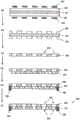
图1是分解表示本发明的一例的蒸镀掩模的金属掩模和树脂掩模的概略立体图,图1的(a)是金属掩模的概略立体图,图1的(b)是树脂掩模的概略立体图。1 is an exploded schematic perspective view of a metal mask and a resin mask of a vapor deposition mask according to an example of the present invention, FIG. 1( a ) is a schematic perspective view of the metal mask, and FIG. 1( b ) is a resin mask Schematic perspective view of .
图2的(a)、图2的(c)、图2的(d)是从表示本发明的一例的蒸镀掩模的金属掩模而视的主视图,图2的(b)是表示本发明的一例的蒸镀掩模的概略剖面图。FIGS. 2( a ), 2 ( c ), and 2 ( d ) are front views seen from a metal mask showing an example of the vapor deposition mask of the present invention, and FIG. 2 ( b ) shows A schematic cross-sectional view of a vapor deposition mask according to an example of the present invention.
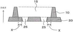
图3是本发明的蒸镀掩模100的扩大剖面图。FIG. 3 is an enlarged cross-sectional view of the
图4的(a)是树脂掩模的另外形态的立体图,图4的(b)是其剖面图。FIG. 4( a ) is a perspective view of another form of the resin mask, and FIG. 4( b ) is a cross-sectional view thereof.
图5是表示本发明的蒸镀掩模100的另外形态的主视图。FIG. 5 is a front view showing another aspect of the
图6是为了说明第1制造方法的工序图,图6的(a)~图6的(f)是均为剖面图。FIG. 6 is a process diagram for explaining the first manufacturing method, and FIGS. 6( a ) to 6 ( f ) are all cross-sectional views.
图7是为了说明第2制造方法的工序图,图7的(a)~图7的(f)是均为剖面图。FIG. 7 is a process diagram for explaining the second manufacturing method, and FIGS. 7( a ) to 7 ( f ) are all cross-sectional views.
图8的(a)~图8的(c)是表示遮挡与和金属掩模的厚度的关系的概略剖面图。FIGS. 8( a ) to 8 ( c ) are schematic cross-sectional views showing the relationship between shielding and the thickness of the metal mask.
图9的(a)~图9的(d)是表示金属掩模的缝隙与树脂掩模的开口部的关系的部分概略剖面图。FIGS. 9( a ) to 9 ( d ) are partial schematic cross-sectional views showing the relationship between the slits of the metal mask and the openings of the resin mask.
图10是表示金属掩模的缝隙与树脂掩模的开口部的关系的部分概略剖面图。10 is a partial schematic cross-sectional view showing the relationship between the slits of the metal mask and the openings of the resin mask.
具体实施方式Detailed ways
以下,对于本发明的蒸镀掩模100,利用附图具体地进行说明。Hereinafter, the
图1的(a)是构成表示本发明的一侧的蒸镀掩模的金属掩模的概略立体图,Fig. 1(a) is a schematic perspective view of a metal mask constituting a vapor deposition mask showing one side of the present invention,
图1的(b)是构成表示本发明的一例的蒸镀掩模的树脂掩模的概略立体图。(b) of FIG. 1 is a schematic perspective view of a resin mask constituting a vapor deposition mask showing an example of the present invention.
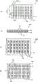
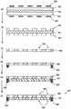
图2的(a)是从表示本发明的一例的蒸镀掩模的金属掩模而视的主视图,图2的(b)是表示本发明的一例的蒸镀掩模的概路剖面图。图3是本发明的蒸镀掩模 100的扩大剖面图。另外,图1~图3为了强调金属掩模所设置的缝隙及设置于蒸镀掩模的开口部,而增加记载相对于整体而言的比率。FIG. 2( a ) is a front view seen from a metal mask showing an example of the vapor deposition mask of the present invention, and FIG. 2( b ) is a schematic cross-sectional view of the vapor deposition mask showing an example of the present invention . Fig. 3 is an enlarged cross-sectional view of the
如图1、图2所示,本发明的蒸镀掩模100层积:设有缝隙15的金属掩模10 和树脂掩模20,该树脂掩模20位于金属掩模10的表面(对于图2的(b)所示的情况是金属掩模10的下面),并且与蒸镀制作的附图相对应的开口部25被纵横配列多个。As shown in FIG. 1 and FIG. 2, the
在此,将本发明的蒸镀掩模100的质量和仅由以往公知的金属所构成的蒸镀掩模的质量,假定蒸镀掩模整体的厚度相同而进行比较,则仅以往公知的蒸镀掩模的金属材料的一部分置换成树脂材料的部分,本发明的蒸镀掩模100 的质量变轻。另外,对于使用仅由金属所构成的蒸镀掩模,为了谋求轻量化,有必要减薄该蒸镀掩模的厚度等,但是,对于减簿蒸镀掩模的厚度在将蒸镀掩模大型化时,蒸镀掩模产生歪曲、耐久性下降的情况。另一方面,根据本发明的蒸镀掩模,即使有做为大型化时的歪曲、要满足耐久性而加厚蒸镀掩模整体厚度的情况,通过树脂掩模20的存在,能够谋求比仅由金属所形成的蒸镀掩模更加轻量化。以下,对于各种结构进行具体地说明。Here, the quality of the
(树脂掩模)(resin mask)
如图1、图2所示,树脂掩模20由树脂构成,对应于蒸镀制作于与缝隙重叠的位置的图案的开口部25被纵横配置多列。然而,在本申请说明书中进行蒸镀制作的图案是指作为用于使用该蒸镀掩模而制作的图案,例如,对于将该蒸镀掩模用于有机电激发光EL元件的有机层的形成情况,是该有机层的形状。另外,在本发明中,举例说明将开口部纵横多列配置的例,开口部25只要是设置于与缝隙重叠的位置即可,而在缝隙15对于仅配置一列于纵向或横向的情况下,只要开口部25被设置于与该一列的缝隙15重叠的位置即可。As shown in FIGS. 1 and 2 , the
树脂掩模20是可适当选择以往公知的树脂材料而使用,对于此材料并无特别限定,可经由激光加工等而形成高精细的开口部25,使用在热或时效的尺寸变化率、吸湿率小并且轻量的材料为优选。作为如此的材料可举出聚酰亚胺树脂,聚酰胺树脂,聚酰胺酰亚胺树脂,聚酯树脂,聚乙烯树脂,聚乙烯醇树脂,聚丙烯树脂,聚碳酸酯树脂,聚苯乙烯树脂,聚丙烯腈树脂,乙烯-乙酸乙烯酯共聚物树脂,乙烯-乙烯醇共聚物树脂,乙烯-甲基丙烯酸共聚物树脂,聚氯乙烯树脂,聚偏氯乙烯树脂,玻璃纸,离聚物树脂等。在上述例举的材料的中,其热膨胀系数为16ppm/℃以下的树脂材料为优选,吸湿率为1.0%以下的树脂材料为优选,而具有此双方条件的树脂材料特别优选。在本发明中,如上所述,树脂掩模20与金属材料比较,由可形成高精细的开口部25的树脂材料构成。因此,可作为具有高精细的开口部25的蒸镀掩模100。The
对于树脂掩模20的厚度也无特别限定,但在使用本发明的蒸镀掩模100而进行蒸镀时,对于为了防止对于蒸镀制成的图案产生不充分的蒸镀部分,也就是成为与作为目的的蒸镀膜厚比较薄的膜厚的蒸镀部分,所谓遮挡的情况,树脂掩模20是尽可能地优选为成为薄的。但对于树脂掩模20的厚度不足3μm 的情况,容易产生有针孔等的缺陷,另外变形等的风险变大。另一方面,当超过25μm时会有遮挡的发生。当考虑此点时,树脂掩模20的厚度是为3μm以上25μm以下为优选。通过树脂掩模20的厚度在该范围内,可降低针孔等的缺陷或变形等的风险,且可有效果地防止遮挡的发生。特别是由将树脂掩模20 的厚度作为3μm以上10μm以下,更优选的是4μm以上8μm以下,由此,可更有效果地防止形成超过300ppi的高精细图案时的遮挡的影响。另外,在本发明的蒸镀掩模100中,金属掩模10与树脂掩模20可直接接合,也可经由粘接剂层结合,但对于经由粘接剂层接合金属掩模10与树脂掩模20的情况,考虑了上述遮挡的情况,树脂掩模20与粘接剂层的合计厚度成为3μm以上25μm以下,优选为3μm以上10μm以下,特别优选设定为4μm以上8μm以下的范围内。The thickness of the
对于开口部25的形状、尺寸并无特别限定,只要是与蒸镀制作的图案的形状、尺寸相对应即可。另外,如图2的(a)所示,对于邻接的开口部25的横向的间距P1,或纵向的间距P2,也可根据蒸镀制作的图案作适当设定。The shape and size of the
对于设置开口部25的位置、开口部25的数量也无特别限定,即使在与缝隙15重叠的位置设置1个也可以,而也可在纵向或者横向设置多个。例如,如图2的(c)所示,缝隙在纵向延伸的情况下,即使在与该缝隙15重叠的开口部25 在横向上设置两个以上也可以。The positions where the
对于开口部25的剖面形状也无特别限定,只要与形成开口部25的树脂掩模的相向的端面彼此为大致平行就可以,但如图2的(b)、图3所示,优选的是,开口部25其剖面形状为具有朝向蒸镀源扩展的形状。换言之,优选的是,是具有朝向金属掩模10侧扩展的锥面。通过将开口部25的剖面形状作为该结构,在使用本发明的蒸镀掩模而进行蒸镀时,可防止在蒸镀作成的图案上产生遮挡。对于锥角θ来说,可考虑树脂掩模20的厚度等而作适当设定,优选的是,连结树脂掩模的开口部的下底前端与同样树脂掩模的开口部的上底前端的角度(θ)在25°~65°的范围内。特别是即使在此范围内中,也优选为小于所使用蒸镀机的蒸镀角度的角度。并且,在图2的(b)、图3中,形成开口部25的端面 25a是呈现直线形状,但并不限定于此,而成为向外凸的弯曲形状,即,开口部25的整体形状成为碗状也是优选的。具有如此剖面形状的开口部25能够形成为,例如在开口部25形成时,能够适当调整激光的照射位置、激光的照射能量,或者进行阶段性地改变照射位置的多阶段的激光照射。The cross-sectional shape of the
由于树脂掩模20使用树脂材料,即使不采用以往的用于金属加工的加工法,例如,蚀刻加工法或切削等的加工方法,也能够形成开口部25。即,对于开口部25的形成方法并无特别限定,可使用各种加工方法,例如,可形成高精细的开口部25的激光加工法、精密冲压加工,光刻加工等而形成开口部 25的方法。对于通过激光加工法等形成开口部25的方法见后述。Since a resin material is used for the
作为蚀刻加工法,例如,可使用从喷射喷嘴,以特定喷雾压力将蚀刻材料进行喷雾的喷涂蚀刻法、浸渍于填充有蚀刻材料的蚀刻液中浸渍蚀刻法、滴下蚀刻材料的旋涂蚀刻法等的湿式蚀刻法、利用气体、等离子体等的干式蚀刻法。As the etching process, for example, spray etching in which the etching material is sprayed from a spray nozzle with a specific spray pressure, immersion etching in an etching solution filled with the etching material, spin coating etching in which the etching material is dropped, etc. can be used. wet etching method, dry etching method using gas, plasma, etc.
另外,在本发明中,由于作为蒸镀掩模100的结构而使用树脂掩模20,所以在使用此蒸镀掩模100进行蒸镀时,对于树脂掩模20的开口部25加以非常高的热,从形成树脂掩模20的开口部25的端面25a(参照图3),产生有气体,有可能产生使蒸镀装置内的真空度降低等的问题。因此,当考虑此点时,如图3所示,对于形成树脂掩模20的开口部25的端面25a是优选设置有阻挡层26。通过形成阻挡层26,可防止产生来自形成树脂掩模20的开口部25的端面25a的气体。In addition, in the present invention, since the
阻挡层26可使用无机氧化物或无机氮化物,金属的薄膜层或蒸镀层。作为无机氧化物可使用铝或硅,铟,锡,镁的氧化物,作为金属可使用铝等。阻挡层26的厚度优选为0.05μm~1μm左右。The
而且,阻挡层优选覆盖树脂掩模20的蒸镀源侧表面。通过以阻挡层26覆盖树脂掩模20的蒸镀源侧表面,更加提高阻挡性。在阻挡层是无机氧化物及无机氮化物的情况下,优选的是利用各种PVD法、CVD法形成。在金属的情况下,优选的是利用真空蒸镀法形成。另外,在此所称的树脂掩模20的蒸镀源侧表面是指树脂掩模20的蒸镀源侧的表面整体就可以,也可为在树脂掩模20的蒸镀源侧的表面,仅从金属掩模露出的部分。Also, the barrier layer preferably covers the vapor deposition source side surface of the
图4的(a)是树脂掩模的另外形态的立体图,图4的(b)是其剖面图。FIG. 4( a ) is a perspective view of another form of the resin mask, and FIG. 4( b ) is a cross-sectional view thereof.
如图4所示,在树脂掩模20上,优选形成有在树脂掩模20的纵向或者横向 (图4的情况是纵向)延伸的槽28。在蒸镀时加热的情况下,树脂掩模20产生热膨胀,由此开口部25的尺寸、位置有可能产生变化,但通过形成该槽28,而可吸收树脂掩模的膨胀,通过在树脂掩模的各处产生的热膨胀产生累积,而可防止树脂掩模20作为整体在特定方向膨胀而改变开口部25的尺寸、位置。As shown in FIG. 4 , the
另外,在图4中,在开口部25之间形成有在纵向延伸的槽28,但并不限定于此,还可以在开口部25之间形成有在横向延伸的槽。另外,并不跟定于开口部25之间,而也可将槽形成在与开口部25重叠的位置。而且,也可以组合这些的形态而构成槽。In addition, in FIG. 4, although the groove|
对于槽28的深度或宽度并无特别限定,但对于槽28深度过深的情况或宽度过宽的情况,由于有树脂掩模20的刚性降低的倾向,所以有必要考虑此点而设定。另外,对于槽的剖面形状也无特别限定,在考虑加工方法等的情况下,而可任意选择U字形状、V字形状等。The depth and width of the
(金属掩模)(metal mask)
金属掩模10是由金属构成,从该金属掩模间的正面而看时,在与开口部25重叠的位置,换言的,在能够看到配置于树脂掩模20的整体的开口部25的位置,多列配置有在纵向或横向延伸的缝隙15。然而,在图1、图2中,在金属掩模10的纵向延伸的缝隙15在横向连续配置。另外,在本发明中,以在纵向或横向延伸的缝隙15作为多列配置的举例,来说明缝隙15,但也可以在纵向或横向仅配置一列缝隙15。The
对于缝隙15的宽度W并无特别限定,但优选的是,至少缝隙15的宽度W 设计为短于邻接的开口部25间的间距。具体来说,如图2的(a)所示,缝隙15 在纵向延伸的情况,优选的是,缝隙15的横向宽度W短于在横向邻接的开口部25的间距P1。同样地,虽未图示,缝隙15在横向延伸的情况下,优选的是缝隙15的纵向的宽度短于在纵向邻接的开口部25的间距P2。另一方面,对于缝隙15在纵向延伸情况的纵向的长度L无特别限定,只要是根据金属掩模10的纵的长度及设置于树脂掩模20的开口部25的位置而作适当设计即可。The width W of the
另外,连续在纵向或者横向延伸的缝隙15可以通过桥接部18分割成多个。然而,图2的(d)是从蒸镀掩模100的金属掩模10侧看到的主视图,表示在图2 的(a)所示的纵向连续延伸的一个缝隙15a通过桥接部18而分割成多个(缝隙 15a、15b)的例。对于桥接部18的宽度并无特别限定,但优选为5μm~20μm左右。通过将轿接器18的宽度设定为此范围,能够有效地提高金属掩模10的刚性。对于桥接部18的配置位置也无特别限定,但分割后的缝隙以与两个以上开口部25重叠地方式配置有桥接部18。In addition, the
对于形成于金属掩模10的缝隙15的剖面形状也无特别限定,但与在上述树脂掩模20的开口部25同样,如图3所示,优选具有朝向蒸镀源扩展的形状。The cross-sectional shape of the
对于金属掩模10的材料并无特别限定,可在蒸镀掩模的领域适当选择利用以往公知的结构,例如,可举出不锈钢,铁镍合金,铝合金等的金属材料。其中,由于铁镍合金的不胀钢热变形小,所以可以适用。The material of the
另外,在使用本发明的蒸镀掩模100对基板进行蒸镀时,在基板后方配置磁铁等,而利用磁力吸引基板前方的蒸镀掩模100为必要的情况下,以磁性体形成金属掩模10为优选。作为磁性体的金属掩模10可举出纯铁,碳素钢,W 钢,Cr钢、Co钢、KS钢、MK钢、NKS钢、Cunico钢、Al-Fe合金等。另外,对于形成金属掩模10的材料本身并非磁性体的情况,也可以通过在该材料分散上述磁性体的粉末,而付与金属掩模10磁性。In addition, when vapor deposition is performed on a substrate using the
对于金属掩模10的厚度并无特别限定,但为5μm~100μm左右为优选。考虑在蒸镀时防止遮挡,优选金属掩模10的厚度是薄的,但作为比5μm薄的情况,破裂或变形的风险提高的同时,有可能操作变为困难。但在本发明中,由于金属掩模10与树脂掩模20一体化,所以,即使金属掩模10的厚度为非常薄的5μm情况,也可使破裂、变形的风险降低,如为5μm以上,则可以使用。然而,对于比100μm厚的情况,因产生遮挡的发生而不优选。The thickness of the
以下,使用图8的(a)~图8的(c),对于遮挡的发生与金属掩模10的厚度的关系具体地进行说明。如图8的(a)所示,在金属掩模10的厚度为薄的情况下,从蒸镀源朝向蒸镀对象物释放的蒸镀材料与金属掩模10的缝隙15的内壁面未冲突,或与未设置金属掩模10的树脂掩模20侧的表面未冲突,而通过金属掩模 10的缝隙15及树脂掩模20的开口部25到达蒸镀对象物。由此,成为可对于蒸镀对象物上,以均一的膜厚形成蒸镀图案。即,可防止遮挡的发生。另一方面,如图8的(b)所示,对于金属掩模10的厚度为厚的情况,例如,金属掩模 10的厚度为超过100μm的情况下,从蒸镀源所释放的蒸镀材料的一部分与金属掩模10的缝隙的的内壁面或与未形成金属掩模10的树脂掩模20侧的表面冲突,而不能到达至蒸镀对象物。不能到达蒸镀对象物的蒸镀材料越多,产生有成为比蒸镀对象物作为目的的蒸镀膜厚为薄的膜厚的未蒸镀部分,而发生有遮挡。Hereinafter, the relationship between the occurrence of shading and the thickness of the
为了充分防止遮挡产生,如图8的(c)所示,将缝隙15的剖面形状作为具有朝向蒸镀源扩展的形状为优选。由作为如此的剖面形状,为了防止在蒸镀掩模100产生的歪曲或者提高耐久性,即使为加厚蒸镀掩模整体厚度的情况,从蒸镀源所释放的蒸镀材料与缝隙15的该表面、与缝隙15的内壁面不进行冲突等,而可使蒸镀材料到达蒸镀对象物。更具体而言,优选连结金属掩模10的缝隙的的下底前端和相同金属掩模10的缝隙15的上底前端的直线与金属掩模 10的底面的所成角度为在25°~65°的范为内。特别是在此范围内之中,优选的是,比所使用的蒸镀机的蒸镀角度小的角度。通过作为如此的剖面形状,为了防止产生于蒸镀掩模100的歪曲或者提高耐久性,即使金属掩模10的厚度为比较厚的情况,从蒸镀源所释放的蒸镀材料也不与缝隙15的内壁面进行冲突等,而可使蒸镀材到达蒸镀对象物。由此,可更有效果地防止遮挡发生。另外,图8是为了说明遮挡的发生与金属掩模10的缝隙15关系的部分概略剖面图。另外,在图8的(c)中,金属掩模10的缝隙15成为具有朝向蒸镀源侧扩展的剖面形状,树脂掩模20的开口部25的相对的端面是成为大致平行,但对于为了更有效果地防止遮挡的发生,金属掩模10的缝隙及树脂掩模20的开口部25 其剖面形状都是优选为具有朝向于蒸镀源侧扩展的形状。In order to sufficiently prevent the occurrence of blocking, as shown in FIG. 8( c ), it is preferable that the cross-sectional shape of the
图5是表示本发明的蒸镀掩模100的另外形态的主视图。FIG. 5 is a front view showing another aspect of the
如图5所示,在从蒸镀掩模100的金属掩模10侧看的主视图中,优选的是,将可从金属掩模的缝隙15所见的形成于树脂掩模20的开口部25相互不同地配置于横向。即,优选将横向邻接的开口部25偏移配置于纵向。通过如此地配置,即使树脂掩模20产生热膨胀的情况,也能够通过开口部25而吸收在各处产生的膨胀,可防止膨胀累积而产生大的变形。As shown in FIG. 5 , in the front view of the
另外,如图5所示,形成于树脂掩模20的开口部25是无需使其对应于一个像素,例如优选汇总两个像素~十个像素对应于一个开口部25。In addition, as shown in FIG. 5, the opening
图9的(a)~图9的(d)是表示金属掩模的缝隙与树脂掩模的开口部的关系的部分概略剖面图,在图示的形态中,由金属掩模的缝隙15和树脂掩模的开口部25所形成的开口整体的剖面形状呈台阶状。如图9所示,通过将开口整体的剖面形状作为具有朝向于蒸镀源侧扩展的台阶状而可有效地防止遮挡的发生。金属掩模的缝隙15、树脂掩模20剖面形状是如图9的(a)所示,优选的是,相对的端面成为大致平行,但如图9的(b)、图9的(c)所示,优选的是,仅金属掩模的缝隙15、树脂掩模的开口部的任一方具有朝向于蒸镀源扩展的剖面形状。另外,如上所说明地那样,如图3或图9的(d)所示,为了更有效地防止遮挡的发生,金属掩模的缝隙15及树脂掩模的开口部25优选为都具有朝向于蒸镀源侧扩展的剖面形状。FIGS. 9( a ) to 9 ( d ) are partial schematic cross-sectional views showing the relationship between the slits of the metal mask and the openings of the resin mask. The cross-sectional shape of the entire opening formed by the opening
对于在成为上述台阶形状的剖面的平坦部(在图9中的符号(X))的宽度并无特别限定,但对于在平坦部(X)的宽度不足lμm的情况下,通过金属掩模的缝隙的干扰,而有防止遮挡发生的效果下降的倾向。因此,当考虑此点时,平坦部(X)的宽度优选为1μm以上。对于优选的上限值无特别限定,而可在考虑树脂掩模的开口部尺寸、邻接的开口部的间隔等之后而作适当设定,作为一例是为20μm左右。The width of the flat portion (symbol (X) in FIG. 9 ) in the cross-section of the above-mentioned stepped shape is not particularly limited, but when the width of the flat portion (X) is less than 1 μm, the width of the flat portion (X) through the metal mask is not particularly limited. There is a tendency that the effect of preventing the occurrence of occlusion decreases due to the interference of the gap. Therefore, considering this point, the width of the flat portion (X) is preferably 1 μm or more. The preferable upper limit is not particularly limited, and can be appropriately set in consideration of the size of the opening of the resin mask, the interval between adjacent openings, and the like, and is about 20 μm as an example.
另外,在上述图9的(a)~图9的(d)中,表示对于缝隙在纵向延伸的情况,与该缝隙15重叠的开口部25作为例子在横向设定为一个,但如图10所示,对于缝隙在纵向延伸的情况,与该缝隙15重叠的开口部25优选在横向设有两个以上。在图10中,金属掩模的缝隙15及树脂掩模的开口部25都具有朝向于蒸镀源侧扩展的剖面形状,与该缝隙15的重叠的开口部25在横向设有两个以上。In addition, in the above-mentioned FIGS. 9(a) to 9(d) , when the slit extends in the vertical direction, the opening
(蒸镀掩模的制造方法)(Manufacturing method of vapor deposition mask)
按着,对于本发明的蒸镀掩模装置的制造方法进行说明。Next, the manufacturing method of the vapor deposition mask apparatus of this invention is demonstrated.
(第1制造方法)(1st manufacturing method)
图6是为了说明第1制造方法的工序图。另外图6的(a)~图6的(f)均为剖面图。FIG. 6 is a process diagram for explaining the first manufacturing method. 6(a) to 6(f) are all cross-sectional views.
第1制造方法是具有:对设有缝隙的金属掩模和树脂板进行贴合的工序;在含有金属的框体上,对贴合有所述树脂板的金属掩模进行固定的工序;从所述金属掩模侧照射激光,在所述树脂板上在纵横形成多列与要蒸镀制作的图案相对应的开口部的工序。以下,对各工序进行说明。The first manufacturing method includes: a step of bonding a metal mask and a resin plate provided with a gap; a step of fixing the metal mask to which the resin plate is bonded to a frame containing metal; A step of irradiating the metal mask side with a laser to form a plurality of rows of openings corresponding to a pattern to be vapor-deposited on the resin plate vertically and horizontally. Hereinafter, each step will be described.
(对设置有缝隙的金属掩模和树脂板进行贴合的工序)(The process of laminating the metal mask and the resin plate with the slits)
首先,准备设置有缝隙的金属掩模。在本方法中,对于准备的金属掩模的制造方法无特别限定,只要适当选择高精度地形成所期望的缝隙的方法即可。First, a metal mask with slits is prepared. In the present method, the method of manufacturing the prepared metal mask is not particularly limited, and a method for forming a desired gap with high accuracy may be appropriately selected.
例如,如图6的(a)所示,准备金属板61,在其两面涂敷抗蚀剂材料62。作为所使用的抗蚀剂材料是使用处理性良好并且具有所期望的解像性的材料。然后,以形成有缝隙图案的掩模63遮蔽抗蚀剂材62,经由密接曝光进行曝光显影。由此,如图6的(b)所示,在金属板61两面形成抗蚀剂图案64。接着,将此抗蚀剂图案作为耐蚀刻掩模而使用,通过两段蚀刻法进行蚀刻加工。另外,两段蚀刻法是指,在金属板的两面形成抗蚀剂图案,在从单面侧进行蚀刻后,在所形成的未贯通的凹部填充耐蚀刻的树脂,填充所谓充填材,然后通过从另一面侧进行蚀刻而形成贯通孔的加工方法。在本方法中,并非只是采用该两段蚀刻法,也可采用从两面同时进行蚀刻的方法,但从加工精度的观点来看,优选使用两段蚀刻法。当蚀刻结束后,洗净除去抗蚀剂图案。由此,如图6的(c)所示,在金属板61形成所期望的缝隙65而得到金属掩模66。For example, as shown in FIG. 6( a ), a
如图6的(d)所示,贴合金属掩模66和树脂板67。对于此方法也无特别限定,例如也可使用各种粘接剂,或使用具有本身粘接性的树脂板。然而,金属掩模66与树脂板的尺寸也可为相同,但之后考虑任意进行框体固定,使树脂板 67的尺寸小于金属掩模66,优选作为露出金属掩模66的外周部分的状态。As shown in FIG.6(d), the
(在含有金属的框体上,对贴合有所述树脂板的金属掩模进行固定的工序)(The process of fixing the metal mask to which the resin plate is bonded to the frame containing metal)
接着,如图6的(e)所示,在含有金属的框体68上,对贴合有树脂板67的金属掩模66进行固定。本方法并无特别限定固定方法,例如,采用点焊等以往公知的工序方法即可。Next, as shown in FIG.6(e), on the
(从金属掩模侧照射激光,在所述树脂板上纵横形成两列以上与蒸镀制作的图案相对应的开口部的工序)(Step of irradiating laser light from the side of the metal mask to form two or more rows of openings corresponding to the pattern produced by vapor deposition on the resin plate vertically and horizontally)
接着,从金属掩模66侧通过缝隙65照射激光,在所述树脂板67上纵横形成两列以上与蒸镀制作的图案相对应的开口部69,而作为树脂掩模70。对于在此所使用的激光装置无特别限定,如使用以往公知的激光装置即可。由此,得到如图6的(f)所示的本发明的蒸镀掩模装置80。Next, laser light is irradiated from the
(第2制造方法)图7是为了说明第2制造方法的工序图。另外图7的(a)~图7 的(f)均为剖面图。(Second Manufacturing Method) FIG. 7 is a process diagram for explaining the second manufacturing method. 7(a) to 7(f) are all cross-sectional views.
第2制造方法具有:在含有金属的框体上,对设置有缝隙的金属掩模进行固定的工序;对固定于所述框体的金属掩模和树脂板进行贴合的工序;从所述金属掩模侧照射激光,将在所述树脂板上与蒸镀制作的图案相对应的开口部被纵横形成多列的工序。也就是,在上述说明的第1制造方法中,在贴合金属掩模66和树脂板67的后,以框体68固定金属掩模66,但在第2制造方法中,首先将金属掩模66固定于框体68,其后贴合树脂板67。The second manufacturing method includes: a step of fixing a metal mask provided with a slit on a frame body containing metal; a step of laminating the metal mask and resin plate fixed to the frame body; A step of irradiating laser light on the metal mask side to form a plurality of rows of openings corresponding to the pattern prepared by vapor deposition on the resin plate. That is, in the first manufacturing method described above, after bonding the
即,在第2制造方法中,如图7的(a)~图7的(c)所示,对于制造金属掩模66 的工序来说,是与所述第1制造方法相同,如图7的(d)所示,将完成的金属掩模66固定于含有金属的框体之后,如图7的(e)所示,贴合金属掩模66和树脂板 67。然后,对于在树脂板67设置开口部65而作为蒸镀掩模装置的工序来说如图7的(f)所示,与所述第l制造方法相同。That is, in the second manufacturing method, as shown in FIGS. 7( a ) to 7 ( c ), the process of manufacturing the
这样,根据第1及第2制造方法,并非将均已完成的蒸镀掩模固定于框体,对于固定于框体的状态的树脂板而言,因在其后设置开口部,可格外地提高位置精度。另外,在以往公知的方法中,为了将决定开口的金属掩模对于框体而言,在拉伸的同时进行固定,而降低开口位置坐标精度。In this way, according to the first and second manufacturing methods, the completed vapor deposition mask is not fixed to the frame body, but the resin plate in the state fixed to the frame body is provided with an opening after that, so it is possible to remarkably Improve location accuracy. In addition, in the conventionally known method, in order to fix the metal mask which determines the opening to the frame while being stretched, the coordinate accuracy of the opening position is lowered.
另外,在以固定于框体的状态的树脂板设置开口部25时,准备预先设有蒸镀制作的图案即与要形成的开口部25相对应的图案的基准板,在将其基准板贴合于未设有树脂板的金属掩模66侧的面的状态下,从金属掩模侧,也可以进行与基准板的图案相对应于的激光照射。根据此方法,可在注视贴合于树脂板的基准板的图案的同时,进行激光照射,在所谓对面配合的状态下,能够形成开口部25,能够形成开口的尺寸精度极高的高精细的开口部25。另外,由于此方法是在固定于框体的状态下进行开口部25的形成,所以可做为不仅尺寸精度而对于位置精度也为良好的蒸镀掩模。In addition, when the
另外,对于使用上述方法的情况,必须可从金属掩模66侧,经由树脂板,由激光照射装置等辨识基准板的图案。作为树脂板对于具有某种程度厚度的情况是成为必须使用具有透明性的材料,但如在上述说明地,对于做为考虑了遮挡的影响的优选的厚度,例如在3μm~25μm左右的厚度的情况下,即使是加以着色的树脂板,也可辨识基准板的图案。In addition, in the case of using the above-mentioned method, it is necessary that the pattern of the reference plate can be recognized from the
对于树脂板和基准板的贴合方法也无特别限定,例如,对于金属掩模66 为磁性体的情况,在基准板的后方配置磁铁等,可吸引树脂板与基准板而进行贴合。除此之外,也可使用静电吸着法等进行贴合。作为基准板可例如举出具有特定的开口图案的TFT基板、光掩模等。The bonding method of the resin plate and the reference plate is also not particularly limited. For example, when the
(轻薄工序)(light and thin process)
另外,在本发明的制造方法中,在上述说明的工序之间或者工序后,进行轻薄工序也可。该工序是在本发明制造方法中的任意的工序,将金属掩模 66的厚度、树脂掩模70的厚度进行最佳化的工序。作为金属掩模66或树脂掩模70的优选的厚度,只要适当设定在上述说明的范围内即可,在此的详细说明省略。In addition, in the production method of the present invention, a thinning step may be performed between or after the steps described above. This step is a step of optimizing the thickness of the
例如,对于作为成为树脂掩模70的树脂板67、成为金属掩模66的金属板 61,使用在上述说明的优选的、厚度较厚的情况,在制造工序中,以单独搬送金属板61、树脂板67时、对于搬送在设有凹部的金属板61上设置树脂板67 的层积体时、或者在搬送在形成上述蒸镀掩模的工序所得到的蒸镀掩模100 时,可付与良好的耐久性、搬送性。另一方面,对于为了防止遮挡的发生等,在本发明的制造方法所得到的蒸镀掩模100的厚度为最佳的厚度为优选。轻薄工序是在制造工序之间或者工序后中,满足耐久性或搬送性的同时,对于将蒸镀掩模100的厚度作为最佳化的情况成为有用的工序。For example, the
成为金属掩模66的金属板61或金属掩模66的轻薄,即,金属掩模的厚度的最佳化,在上述所说明的工序之间或者工序后,可将与金属板61的树脂板 67不相接一侧的面,或者与金属掩模66的树脂板67或树脂掩模20不相接一侧的面,通过使用能够蚀刻金属板61、金属掩模66的蚀刻材料进行蚀刻而能够实现。The thinning of the
对于成为树脂掩模70的树脂板67或树脂掩模70的轻薄,即树脂板67、树脂掩模70的厚度的最佳化也为同样,可由于在上述所说明的任何工序之间或者工序后,可将与树脂板们的金属板61或金属掩模66不相接一侧的面,或者与树脂掩模70的金属掩模66不相接一侧的面,使用能够蚀刻树脂板67、树脂掩模70的材料的蚀刻材料进行蚀刻而能够实现。另外,在形成蒸镀掩模100之后,通过蚀刻加工金属掩模66、树脂掩模70双方,也可将双方的厚度进行最佳化。The same applies to the thinness of the
(有机半导体元件的制造方法)(Manufacturing method of organic semiconductor element)
本发明的有机半导体元件的制造方法,是使用在上述说明的本发明的蒸镀掩模100而形成有机半导体元件为特征的方法。对于蒸镀掩模100是可直接使用在上述说明的本发明的蒸镀掩模100,在此的详细说明是省略的。根据在上述所说明的本发明的蒸镀掩模,利用该蒸镀掩模100所具有的尺寸精度高的开口部25,可形成具有高精细图案的有机半导体元件。作为以本发明的制造方法所制造的有机半导体元件,例如,可举出有机电激发光EL元件的有机层、发光层、阴极电极等。特别是本发明的有机半导体元件的制造方法是可最佳地用于要求高精细图案精度的有机电激发光EL元件的R、G、B发光层的制造。The manufacturing method of the organic semiconductor element of this invention is a method characterized by forming an organic semiconductor element using the
附图标记说明Description of reference numerals
100:蒸镀掩模100: Evaporation mask
10、66:金属掩模10, 66: Metal Mask
15:缝隙15: Gap
18:桥接部18: Bridge section
20、70:树脂掩模20, 70: Resin mask
25:开口部25: Opening
80:蒸镀掩模装置80: Evaporation mask device
Claims (9)
Translated fromChineseApplications Claiming Priority (3)
| Application Number | Priority Date | Filing Date | Title |
|---|---|---|---|
| JP2012004484 | 2012-01-12 | ||
| JP2012-004484 | 2012-01-12 | ||
| CN201380005292.1ACN104053813B (en) | 2012-01-12 | 2013-01-11 | Evaporation mask, method of manufacturing vapor deposition mask device, and method of manufacturing organic semiconductor element |
Related Parent Applications (1)
| Application Number | Title | Priority Date | Filing Date |
|---|---|---|---|
| CN201380005292.1ADivisionCN104053813B (en) | 2012-01-12 | 2013-01-11 | Evaporation mask, method of manufacturing vapor deposition mask device, and method of manufacturing organic semiconductor element |
Publications (2)
| Publication Number | Publication Date |
|---|---|
| CN105336855A CN105336855A (en) | 2016-02-17 |
| CN105336855Btrue CN105336855B (en) | 2020-08-04 |
Family
ID=48781584
Family Applications (9)
| Application Number | Title | Priority Date | Filing Date |
|---|---|---|---|
| CN201510639737.2AActiveCN105336855B (en) | 2012-01-12 | 2013-01-11 | Evaporation mask device preparation body |
| CN201510639770.5APendingCN105331934A (en) | 2012-01-12 | 2013-01-11 | Vapor deposition mask, method for producing vapor deposition mask device and method for producing organic semiconductor element |
| CN201510639577.1AActiveCN105322102B (en) | 2012-01-12 | 2013-01-11 | The manufacturing method of deposition mask device |
| CN201510639578.6AActiveCN105322103B (en) | 2012-01-12 | 2013-01-11 | Evaporation mask and method for producing organic semiconductor element |
| CN201510639565.9APendingCN105349946A (en) | 2012-01-12 | 2013-01-11 | Vapor deposition mask method for producing organic semiconductor element |
| CN201510639576.7AActiveCN105322101B (en) | 2012-01-12 | 2013-01-11 | The manufacturing method of deposition mask and organic semiconductor device |
| CN201380005292.1AActiveCN104053813B (en) | 2012-01-12 | 2013-01-11 | Evaporation mask, method of manufacturing vapor deposition mask device, and method of manufacturing organic semiconductor element |
| CN201510639596.4AActiveCN105331927B (en) | 2012-01-12 | 2013-01-11 | Deposition mask prepares body |
| CN201510639768.8AActiveCN105331928B (en) | 2012-01-12 | 2013-01-11 | The manufacturing method of deposition mask device and organic semiconductor device |
Family Applications After (8)
| Application Number | Title | Priority Date | Filing Date |
|---|---|---|---|
| CN201510639770.5APendingCN105331934A (en) | 2012-01-12 | 2013-01-11 | Vapor deposition mask, method for producing vapor deposition mask device and method for producing organic semiconductor element |
| CN201510639577.1AActiveCN105322102B (en) | 2012-01-12 | 2013-01-11 | The manufacturing method of deposition mask device |
| CN201510639578.6AActiveCN105322103B (en) | 2012-01-12 | 2013-01-11 | Evaporation mask and method for producing organic semiconductor element |
| CN201510639565.9APendingCN105349946A (en) | 2012-01-12 | 2013-01-11 | Vapor deposition mask method for producing organic semiconductor element |
| CN201510639576.7AActiveCN105322101B (en) | 2012-01-12 | 2013-01-11 | The manufacturing method of deposition mask and organic semiconductor device |
| CN201380005292.1AActiveCN104053813B (en) | 2012-01-12 | 2013-01-11 | Evaporation mask, method of manufacturing vapor deposition mask device, and method of manufacturing organic semiconductor element |
| CN201510639596.4AActiveCN105331927B (en) | 2012-01-12 | 2013-01-11 | Deposition mask prepares body |
| CN201510639768.8AActiveCN105331928B (en) | 2012-01-12 | 2013-01-11 | The manufacturing method of deposition mask device and organic semiconductor device |
Country Status (6)
| Country | Link |
|---|---|
| US (7) | US9108216B2 (en) |
| JP (7) | JP5288072B2 (en) |
| KR (6) | KR102128735B1 (en) |
| CN (9) | CN105336855B (en) |
| TW (7) | TWI622662B (en) |
| WO (1) | WO2013105642A1 (en) |
Families Citing this family (106)
| Publication number | Priority date | Publication date | Assignee | Title |
|---|---|---|---|---|
| TWI461098B (en)* | 2012-01-12 | 2014-11-11 | Dainippon Printing Co Ltd | A method of manufacturing a vapor deposition mask, and a method of manufacturing an organic semiconductor device |
| CN105296920B (en) | 2012-01-12 | 2018-03-06 | 大日本印刷株式会社 | Layout deposition mask |
| CN105336855B (en)* | 2012-01-12 | 2020-08-04 | 大日本印刷株式会社 | Evaporation mask device preparation body |
| JP5895539B2 (en)* | 2012-01-12 | 2016-03-30 | 大日本印刷株式会社 | Evaporation mask |
| JP5895540B2 (en)* | 2012-01-12 | 2016-03-30 | 大日本印刷株式会社 | Evaporation mask |
| TWI671414B (en)* | 2013-03-26 | 2019-09-11 | 日商大日本印刷股份有限公司 | Vapor deposition mask, vapor deposition mask preparation body, method for producing vapor deposition mask, and method for producing organic semiconductor device |
| CN107855641A (en)* | 2013-04-12 | 2018-03-30 | 大日本印刷株式会社 | Deposition mask, deposition mask prepare body, the manufacture method of deposition mask and the manufacture method of organic semiconductor device |
| TWI624557B (en)* | 2013-04-12 | 2018-05-21 | 大日本印刷股份有限公司 | Vapor deposition mask, vapor deposition mask preparation body, method for manufacturing vapor deposition mask, and method for manufacturing organic semiconductor element |
| JP5455099B1 (en) | 2013-09-13 | 2014-03-26 | 大日本印刷株式会社 | Metal plate, metal plate manufacturing method, and mask manufacturing method using metal plate |
| JP6168944B2 (en)* | 2013-09-20 | 2017-07-26 | 株式会社ブイ・テクノロジー | Deposition mask |
| JP6331312B2 (en)* | 2013-09-30 | 2018-05-30 | 大日本印刷株式会社 | Vapor deposition mask manufacturing method and vapor deposition mask preparation |
| JP2015067892A (en)* | 2013-09-30 | 2015-04-13 | 大日本印刷株式会社 | Vapor deposition mask and organic semiconductor device manufacturing method |
| JP6394877B2 (en)* | 2013-09-30 | 2018-09-26 | 大日本印刷株式会社 | Vapor deposition mask, vapor deposition mask manufacturing method, vapor deposition mask preparation, framed vapor deposition mask, and organic semiconductor element manufacturing method |
| JP2015074826A (en)* | 2013-10-11 | 2015-04-20 | 株式会社ブイ・テクノロジー | Deposition mask, and manufacturing method thereof |
| JP5516816B1 (en) | 2013-10-15 | 2014-06-11 | 大日本印刷株式会社 | Metal plate, method for producing metal plate, and method for producing vapor deposition mask using metal plate |
| JP5780350B2 (en)* | 2013-11-14 | 2015-09-16 | 大日本印刷株式会社 | Vapor deposition mask, vapor deposition mask with frame, and method of manufacturing organic semiconductor element |
| JP6409701B2 (en)* | 2013-11-14 | 2018-10-24 | 大日本印刷株式会社 | Vapor deposition mask, vapor deposition mask with frame, and method of manufacturing organic semiconductor element |
| JP6288497B2 (en)* | 2013-12-13 | 2018-03-07 | 株式会社ブイ・テクノロジー | Mask and manufacturing method thereof |
| JP6357312B2 (en) | 2013-12-20 | 2018-07-11 | 株式会社ブイ・テクノロジー | Method for manufacturing film formation mask and film formation mask |
| KR102138625B1 (en)* | 2013-12-23 | 2020-07-29 | 엘지디스플레이 주식회사 | Thin film forming apparatus |
| JP5846287B1 (en)* | 2013-12-27 | 2016-01-20 | 大日本印刷株式会社 | Manufacturing method of vapor deposition mask with frame, tension device, manufacturing apparatus of organic semiconductor element, and manufacturing method of organic semiconductor element |
| JP6240960B2 (en)* | 2014-02-03 | 2017-12-06 | 株式会社ブイ・テクノロジー | Method for manufacturing film formation mask and film formation mask |
| JP6347112B2 (en)* | 2014-02-07 | 2018-06-27 | 大日本印刷株式会社 | Vapor deposition mask, vapor deposition mask preparation, vapor deposition mask manufacturing method, pattern manufacturing method, framed vapor deposition mask, and organic semiconductor element manufacturing method |
| JP2015148002A (en)* | 2014-02-07 | 2015-08-20 | 大日本印刷株式会社 | Vapor deposition mask, vapor deposition mask preparation, and method for manufacturing organic semiconductor element |
| CN103882375B (en)* | 2014-03-12 | 2016-03-09 | 京东方科技集团股份有限公司 | A kind of mask plate and preparation method thereof |
| JP6326885B2 (en)* | 2014-03-19 | 2018-05-23 | 大日本印刷株式会社 | Vapor deposition mask, vapor deposition mask preparation, and method for manufacturing organic semiconductor element |
| JP6511908B2 (en)* | 2014-03-31 | 2019-05-15 | 大日本印刷株式会社 | Tension method of deposition mask, method of manufacturing deposition mask with frame, method of manufacturing organic semiconductor device, and tension device |
| CN103952666B (en)* | 2014-04-22 | 2016-02-10 | 四川虹视显示技术有限公司 | evaporation mask plate tensioning method |
| CN103981485B (en)* | 2014-05-09 | 2016-07-06 | 合肥鑫晟光电科技有限公司 | Mask plate and manufacture method thereof |
| JP5641462B1 (en) | 2014-05-13 | 2014-12-17 | 大日本印刷株式会社 | Metal plate, metal plate manufacturing method, and mask manufacturing method using metal plate |
| CN110331365B (en)* | 2014-06-06 | 2021-10-01 | 大日本印刷株式会社 | Evaporation mask, precursor thereof, and method for producing organic semiconductor element |
| WO2015186632A1 (en)* | 2014-06-06 | 2015-12-10 | 大日本印刷株式会社 | Vapor deposition mask, vapor deposition mask with frame, vapor deposition mask precursor, and method for manufacturing organic semiconductor element |
| JP6323266B2 (en)* | 2014-09-03 | 2018-05-16 | 大日本印刷株式会社 | Deposition mask inspection method |
| US20170311411A1 (en)* | 2014-10-23 | 2017-10-26 | Sharp Kabushiki Kaisha | Deposition-mask manufacturing method, deposition mask, deposition device, and deposition method |
| DE102014116076A1 (en)* | 2014-11-04 | 2016-05-04 | Osram Opto Semiconductors Gmbh | Method for applying a material to a surface |
| JP6375906B2 (en)* | 2014-12-02 | 2018-08-22 | 大日本印刷株式会社 | Vapor deposition mask, vapor deposition mask preparation, framed vapor deposition mask, and organic semiconductor device manufacturing method |
| WO2016117535A1 (en)* | 2015-01-20 | 2016-07-28 | シャープ株式会社 | Deposition mask, manufacturing method |
| JP5994952B2 (en)* | 2015-02-03 | 2016-09-21 | 大日本印刷株式会社 | Vapor deposition mask manufacturing method, vapor deposition mask manufacturing apparatus, laser mask, and organic semiconductor element manufacturing method |
| EP3257964B1 (en)* | 2015-02-10 | 2019-11-13 | Dai Nippon Printing Co., Ltd. | Manufacturing method for deposition mask, metal sheet used for producing deposition mask, and manufacturing method for said metal sheet |
| JP6163586B2 (en) | 2015-04-17 | 2017-07-12 | 大日本印刷株式会社 | Deposition method of vapor deposition pattern, pressing member integrated with pressing plate, vapor deposition apparatus and organic semiconductor element manufacturing method |
| CH711107A1 (en)* | 2015-05-20 | 2016-11-30 | Glas Trösch Holding AG | Coupling device for thermogravimetric analysis. |
| JP2017008342A (en)* | 2015-06-17 | 2017-01-12 | 株式会社ブイ・テクノロジー | Film deposition mask and production method of film deposition mask |
| CN112267091B (en)* | 2015-07-03 | 2023-02-17 | 大日本印刷株式会社 | Method for manufacturing vapor deposition mask, method for manufacturing organic semiconductor element, method for manufacturing organic EL display, vapor deposition mask preparation body, and vapor deposition mask |
| JP6160747B2 (en)* | 2015-07-03 | 2017-07-12 | 大日本印刷株式会社 | Vapor deposition mask manufacturing method, vapor deposition mask preparation, organic semiconductor element manufacturing method, and vapor deposition mask |
| WO2017045122A1 (en)* | 2015-09-15 | 2017-03-23 | Applied Materials, Inc. | A shadow mask for organic light emitting diode manufacture |
| KR102430444B1 (en) | 2015-12-18 | 2022-08-09 | 삼성디스플레이 주식회사 | A mask assembly, apparatus and method for manufacturing a display apparatus using the same |
| CN112030102B (en)* | 2016-02-10 | 2022-12-06 | 鸿海精密工业股份有限公司 | Manufacturing method of evaporation mask |
| JP2017150017A (en) | 2016-02-23 | 2017-08-31 | 株式会社ジャパンディスプレイ | Method for manufacturing vapor deposition mask and method for manufacturing organic EL display |
| US20200299821A1 (en)* | 2016-03-18 | 2020-09-24 | Hon Hai Precision Industry Co., Ltd. | Vapor deposition mask, method for producing vapor deposition mask, and method for producing organic semiconductor element |
| WO2017168773A1 (en) | 2016-03-29 | 2017-10-05 | 鴻海精密工業股▲ふん▼有限公司 | Vapor deposition mask, method for manufacturing vapor deposition mask, vapor deposition method, and method for manufacturing organic el display device |
| JP6465075B2 (en) | 2016-05-26 | 2019-02-06 | 大日本印刷株式会社 | Vapor deposition mask, vapor deposition mask with frame, method for producing organic semiconductor element, and method for producing organic EL display |
| WO2018003766A1 (en) | 2016-06-28 | 2018-01-04 | 大日本印刷株式会社 | Vapor deposition mask, method for manufacturing organic semiconductor element, and method for manufacturing organic el display |
| JP7017032B2 (en) | 2016-06-28 | 2022-02-08 | 大日本印刷株式会社 | A vapor deposition mask, a method for manufacturing an organic semiconductor device, and a method for manufacturing an organic EL display. |
| KR102632617B1 (en)* | 2016-08-08 | 2024-02-02 | 삼성디스플레이 주식회사 | Mask assembly, apparatus and method for manufacturing a display apparatus using the same and display apparatus |
| KR102624714B1 (en) | 2016-09-12 | 2024-01-12 | 삼성디스플레이 주식회사 | Mask and method for preparing the mask assembly having the same |
| CN118159109A (en) | 2016-09-13 | 2024-06-07 | Lg伊诺特有限公司 | Metal plate for deposition mask, deposition mask and method for manufacturing the same |
| KR102455363B1 (en) | 2016-09-29 | 2022-10-18 | 다이니폰 인사츠 가부시키가이샤 | Vapor deposition mask package and vapor deposition mask packaging method |
| WO2018062300A1 (en)* | 2016-09-30 | 2018-04-05 | 大日本印刷株式会社 | Evaporation mask, evaporation mask provided with frame, evaporation mask prepared body, method for forming vapor deposition pattern, method for manufacturing organic semiconductor element, and method for manufacturing organic el display |
| WO2018058521A1 (en)* | 2016-09-30 | 2018-04-05 | 深圳市柔宇科技有限公司 | Metal mask for oled evaporation deposition and oled evaporation deposition method |
| JP6922179B2 (en)* | 2016-09-30 | 2021-08-18 | 大日本印刷株式会社 | A method for manufacturing a vapor deposition mask, an organic semiconductor element, and a method for manufacturing an organic EL display. |
| JP6926435B2 (en)* | 2016-10-03 | 2021-08-25 | 大日本印刷株式会社 | A method for manufacturing a vapor deposition mask, a method for manufacturing an organic semiconductor element, and a method for manufacturing an organic EL display. |
| CN109790615A (en) | 2016-10-06 | 2019-05-21 | 大日本印刷株式会社 | The manufacturing method of the manufacturing method of deposition mask, the manufacturing method of organic semiconductor device and organic el display |
| EP3524710B8 (en) | 2016-10-07 | 2024-01-24 | Dai Nippon Printing Co., Ltd. | Method of manufacturing deposition mask, intermediate product to which deposition mask is allocated, and deposition mask |
| US20180183014A1 (en)* | 2016-12-27 | 2018-06-28 | Int Tech Co., Ltd. | Light emitting device |
| JP6620899B2 (en)* | 2017-03-31 | 2019-12-18 | 大日本印刷株式会社 | Vapor deposition mask, vapor deposition mask with frame, vapor deposition mask preparation, vapor deposition pattern forming method, and organic semiconductor element manufacturing method |
| CN107058945B (en)* | 2017-04-20 | 2020-07-07 | 京东方科技集团股份有限公司 | Mask plate |
| CN206706184U (en)* | 2017-05-12 | 2017-12-05 | 京东方科技集团股份有限公司 | Mask plate and mask sheet |
| KR102300029B1 (en)* | 2017-07-27 | 2021-09-09 | 삼성디스플레이 주식회사 | Mask frame assembly, method for manufacturing the same and method for manufacturing a display apparatus using the same |
| US20190044068A1 (en)* | 2017-08-01 | 2019-02-07 | Wuhan China Star Optoelectronics Semiconductor Dis play Technology Co., Ltd. | Mask plate |
| US10510959B2 (en) | 2017-08-22 | 2019-12-17 | Wuhan China Star Optoelectronics Semiconductor Display Technology Co., Ltd. | Commissioning method and vapor deposition machine |
| CN107523787B (en)* | 2017-08-22 | 2019-08-02 | 武汉华星光电半导体显示技术有限公司 | A kind of adjustment method and evaporator |
| JP6300257B1 (en)* | 2017-08-31 | 2018-03-28 | 堺ディスプレイプロダクト株式会社 | Method for manufacturing film-forming mask |
| JP6497596B2 (en)* | 2017-09-14 | 2019-04-10 | 大日本印刷株式会社 | Intermediate of vapor deposition mask device |
| KR102411536B1 (en)* | 2017-10-11 | 2022-06-22 | 삼성디스플레이 주식회사 | Deposition mask manufacturing method and manufacturing apparatus thereof |
| US11121321B2 (en)* | 2017-11-01 | 2021-09-14 | Emagin Corporation | High resolution shadow mask with tapered pixel openings |
| KR102399595B1 (en)* | 2017-11-21 | 2022-05-19 | 엘지이노텍 주식회사 | Metal substrate and mask using the same |
| US10876199B2 (en)* | 2017-12-25 | 2020-12-29 | Sakai Display Products Corporation | Vapor deposition mask, vapor deposition method, and production method for organic EL display device |
| CN108227989B (en)* | 2018-01-02 | 2021-03-05 | 京东方科技集团股份有限公司 | Touch substrate and preparation method thereof, metal mask plate and display device |
| CN108281575B (en)* | 2018-01-26 | 2020-08-14 | 京东方科技集团股份有限公司 | Mask plate and manufacturing method thereof |
| JP6583446B2 (en)* | 2018-01-31 | 2019-10-02 | 大日本印刷株式会社 | Vapor deposition mask and organic semiconductor device manufacturing method |
| JP6996997B2 (en) | 2018-02-03 | 2022-01-17 | 日鉄ケミカル&マテリアル株式会社 | Metal-clad laminate and its manufacturing method |
| JP6658790B2 (en)* | 2018-04-19 | 2020-03-04 | 大日本印刷株式会社 | Evaporation mask, evaporation mask with frame, evaporation mask preparation, method of manufacturing evaporation mask, method of manufacturing organic semiconductor element, method of manufacturing organic EL display, and method of forming pattern |
| CN108914055B (en)* | 2018-07-05 | 2020-07-17 | 京东方科技集团股份有限公司 | A mask and evaporation equipment |
| JP7110776B2 (en)* | 2018-07-11 | 2022-08-02 | 大日本印刷株式会社 | Vapor deposition mask, method for manufacturing vapor deposition mask, and method for manufacturing organic EL display device |
| CN109166984A (en)* | 2018-09-12 | 2019-01-08 | 苏州蓝沛光电科技有限公司 | Mask and its manufacturing method for oled panel |
| CN109161853B (en)* | 2018-09-25 | 2020-12-18 | 合肥京东方光电科技有限公司 | Vapor deposition equipment and vapor deposition method |
| KR102137168B1 (en)* | 2018-10-15 | 2020-07-24 | 엘지전자 주식회사 | Processing method for fine metal mask and fine metal mask using the same |
| CN109208888A (en)* | 2018-10-22 | 2019-01-15 | 中国二冶集团有限公司 | The waste and old template reuse means of architectural engineering |
| US11773477B2 (en) | 2018-12-25 | 2023-10-03 | Dai Nippon Printing Co., Ltd. | Deposition mask |
| CN111378924A (en)* | 2018-12-25 | 2020-07-07 | 大日本印刷株式会社 | Vapor deposition mask |
| US11056277B2 (en) | 2018-12-28 | 2021-07-06 | Applied Materials, Inc. | Magnetized substrate carrier apparatus with shadow mask for deposition |
| CN109746141A (en)* | 2019-01-29 | 2019-05-14 | 杨鑫鹏 | A wood grain spraying board for furniture paint surface maintenance and spraying method and manufacturing process thereof |
| CN109881147A (en)* | 2019-02-01 | 2019-06-14 | 云谷(固安)科技有限公司 | Vapor deposition mask plate, preparation method, oled display substrate and display device |
| US10957512B1 (en)* | 2019-09-25 | 2021-03-23 | Applied Materials, Inc. | Method and device for a carrier proximity mask |
| CN210916231U (en)* | 2019-10-18 | 2020-07-03 | 昆山国显光电有限公司 | Mask plate |
| US11805678B2 (en) | 2019-11-21 | 2023-10-31 | Samsung Display Co., Ltd. | Display device, mask assembly, method of manufacturing the mask assembly, apparatus for manufacturing the display device, and method of manufacturing the display device |
| US20230043183A1 (en)* | 2020-01-03 | 2023-02-09 | Hunetplus Co., Ltd. | Flexible photo-patterned mask for organic light emitting display with high resolution and method for manufacturing the same |
| KR20210091382A (en) | 2020-01-13 | 2021-07-22 | 삼성디스플레이 주식회사 | Mask, method of manufacturing the same, and method of manufacturing display panel |
| KR20210113526A (en)* | 2020-03-06 | 2021-09-16 | 삼성디스플레이 주식회사 | Method of manufacturing mask, mask manufacture by the same, and method of manufacturing display apparatus |
| JP7749925B2 (en)* | 2020-03-13 | 2025-10-07 | 大日本印刷株式会社 | Evaluation method for deposition chamber of organic device manufacturing equipment |
| CN113817981B (en)* | 2020-06-18 | 2022-09-30 | 中国科学技术大学 | Mask and method of making the same |
| KR20220016383A (en)* | 2020-07-31 | 2022-02-09 | 삼성디스플레이 주식회사 | Mask and manufacturing method of mask |
| CN113224105B (en)* | 2021-07-08 | 2021-09-28 | 苏州芯聚半导体有限公司 | Colorization manufacturing method, color substrate and display device |
| KR20230020035A (en)* | 2021-08-02 | 2023-02-10 | 삼성디스플레이 주식회사 | Mask for Deposition |
| US20250146121A1 (en) | 2022-01-31 | 2025-05-08 | Dai Nippon Printing Co., Ltd. | Mask and method of manufacturing mask |
| JPWO2024128182A1 (en) | 2022-12-13 | 2024-06-20 |
Citations (1)
| Publication number | Priority date | Publication date | Assignee | Title |
|---|---|---|---|---|
| JP2004190057A (en)* | 2002-12-09 | 2004-07-08 | Nippon Filcon Co Ltd | Mask for forming thin film pattern of lamination structure comprising patterned mask film and supporting body, and its manufacturing method |
Family Cites Families (78)
| Publication number | Priority date | Publication date | Assignee | Title |
|---|---|---|---|---|
| JPS5948059A (en) | 1982-09-13 | 1984-03-19 | Dainippon Ink & Chem Inc | Modified stevioside |
| JPS6376859A (en)* | 1986-09-19 | 1988-04-07 | Matsushita Electric Ind Co Ltd | Vapor deposition mask and its manufacturing method |
| JP3017752B2 (en) | 1989-07-26 | 2000-03-13 | 村上スクリーン株式会社 | Printing metal mask and manufacturing method thereof |
| JPH07300664A (en)* | 1994-04-28 | 1995-11-14 | Fujitsu Ltd | Metal mask manufacturing method and its reclaiming method |
| US6045671A (en)* | 1994-10-18 | 2000-04-04 | Symyx Technologies, Inc. | Systems and methods for the combinatorial synthesis of novel materials |
| DE69618162T2 (en) | 1995-08-24 | 2002-08-14 | Kabushiki Kaisha Toshiba, Kawasaki | Manufacturing process of a reflector |
| JPH09143758A (en) | 1995-11-22 | 1997-06-03 | Nippon Steel Corp | Resin-coated metal plate for container and can body having the resin-coated metal plate |
| JP2000173769A (en) | 1998-12-03 | 2000-06-23 | Toray Ind Inc | Manufacture of organic electric field light-emitting element |
| US6469439B2 (en) | 1999-06-15 | 2002-10-22 | Toray Industries, Inc. | Process for producing an organic electroluminescent device |
| US20100261159A1 (en)* | 2000-10-10 | 2010-10-14 | Robert Hess | Apparatus for assay, synthesis and storage, and methods of manufacture, use, and manipulation thereof |
| JP2002220656A (en) | 2000-11-22 | 2002-08-09 | Sanyo Electric Co Ltd | Mask for vapor deposition and manufacturing method therefor |
| JP4092914B2 (en) | 2001-01-26 | 2008-05-28 | セイコーエプソン株式会社 | MASK MANUFACTURING METHOD, ORGANIC ELECTROLUMINESCENT DEVICE MANUFACTURING METHOD |
| US7396558B2 (en) | 2001-01-31 | 2008-07-08 | Toray Industries, Inc. | Integrated mask and method and apparatus for manufacturing organic EL device using the same |
| JP4096567B2 (en) | 2001-01-31 | 2008-06-04 | 東レ株式会社 | Integrated mask, method for manufacturing organic EL element using integrated mask, and manufacturing apparatus therefor |
| JP4635348B2 (en)* | 2001-02-08 | 2011-02-23 | 凸版印刷株式会社 | Pattern forming mask and pattern forming apparatus using the same |
| JP2003332057A (en) | 2002-05-16 | 2003-11-21 | Dainippon Printing Co Ltd | Multi-face mask device for vacuum deposition used for manufacturing organic EL devices |
| CN100355104C (en)* | 2001-08-24 | 2007-12-12 | 大日本印刷株式会社 | Multi-face forming mask device for vacuum deposition |
| JP2003231964A (en) | 2001-12-05 | 2003-08-19 | Toray Ind Inc | Evaporation mask, its manufacturing process, organic electroluminescent device and its manufacturing process |
| KR100490534B1 (en) | 2001-12-05 | 2005-05-17 | 삼성에스디아이 주식회사 | Mask frame assembly for thin layer vacuum evaporation of Organic electro luminescence device |
| US6897164B2 (en) | 2002-02-14 | 2005-05-24 | 3M Innovative Properties Company | Aperture masks for circuit fabrication |
| JP2003272838A (en)* | 2002-03-14 | 2003-09-26 | Dainippon Printing Co Ltd | Masking material |
| JP2004043898A (en) | 2002-07-12 | 2004-02-12 | Canon Electronics Inc | Vapor deposition mask, and organic electroluminescence display device |
| JP2004055231A (en)* | 2002-07-17 | 2004-02-19 | Dainippon Printing Co Ltd | Multi-faced metal mask for vacuum deposition used for manufacturing organic EL devices |
| JP3990307B2 (en)* | 2003-03-24 | 2007-10-10 | 株式会社クラレ | Manufacturing method of resin molded product, manufacturing method of metal structure, chip |
| KR100534580B1 (en) | 2003-03-27 | 2005-12-07 | 삼성에스디아이 주식회사 | Deposition mask for display device and Method for fabricating the same |
| JPWO2004114021A1 (en)* | 2003-06-23 | 2006-08-03 | 三井化学株式会社 | Photosensitive composition and method for producing printed wiring board using the same |
| US9236279B2 (en) | 2003-06-27 | 2016-01-12 | Lam Research Corporation | Method of dielectric film treatment |
| JP2005042147A (en)* | 2003-07-25 | 2005-02-17 | Dainippon Screen Mfg Co Ltd | Method of producing mask for vapor deposition, and mask for vapor deposition |
| JP2005146338A (en)* | 2003-11-14 | 2005-06-09 | Sony Corp | Vapor deposition mask |
| JP2005154879A (en)* | 2003-11-28 | 2005-06-16 | Canon Components Inc | Metal mask for vapor deposition, and method of producing vapor deposition pattern using the same |
| JP2005174843A (en) | 2003-12-15 | 2005-06-30 | Sony Corp | Deposition mask and its manufacturing method |
| JP4434809B2 (en)* | 2004-03-29 | 2010-03-17 | 三洋電機株式会社 | Manufacturing method of semiconductor device |
| JP2008226859A (en)* | 2004-10-22 | 2008-09-25 | Seiko Epson Corp | Method for manufacturing organic electroluminescence device and organic electroluminescence device |
| JP4329740B2 (en) | 2004-10-22 | 2009-09-09 | セイコーエプソン株式会社 | Method for manufacturing organic electroluminescent device and organic electroluminescent device |
| JP4761569B2 (en) | 2004-12-21 | 2011-08-31 | アルバック シンガポール プライベート リミテッド | Deposition mask and mask assembly jig |
| JP4438710B2 (en) | 2005-07-20 | 2010-03-24 | セイコーエプソン株式会社 | Mask, mask chip, mask manufacturing method, and mask chip manufacturing method |
| JP5008849B2 (en) | 2005-09-08 | 2012-08-22 | ソニーモバイルディスプレイ株式会社 | Laser processing method and manufacturing method of display device having transparent resin layer |
| US20070148337A1 (en) | 2005-12-22 | 2007-06-28 | Nichols Jonathan A | Flame-perforated aperture masks |
| CN100482848C (en)* | 2006-06-12 | 2009-04-29 | 友达光电股份有限公司 | Shielding, evaporation device using same and manufacturing method of display panel |
| JP2008121060A (en)* | 2006-11-10 | 2008-05-29 | Mitsubishi Paper Mills Ltd | Method of manufacturing vacuum film-forming mask with resin and vacuum film-forming mask with resin |
| KR20080045886A (en)* | 2006-11-21 | 2008-05-26 | 삼성전자주식회사 | Mask for organic film deposition and manufacturing method thereof, and manufacturing method of organic light emitting display device comprising same |
| JP5255224B2 (en) | 2007-03-29 | 2013-08-07 | 三菱製紙株式会社 | Screen printing mask and method for producing screen printing mask |
| JP2008255449A (en)* | 2007-04-09 | 2008-10-23 | Kyushu Hitachi Maxell Ltd | Vapor deposition mask and manufacturing method thereof |
| CN100580905C (en) | 2007-04-20 | 2010-01-13 | 晶能光电(江西)有限公司 | Method for obtaining high quality margins of semiconductor devices fabricated on segmented substrates |
| JP2008274373A (en)* | 2007-05-02 | 2008-11-13 | Optnics Precision Co Ltd | Mask for vapor deposition |
| KR20080111967A (en) | 2007-06-20 | 2008-12-24 | 삼성전기주식회사 | Shadow mask |
| JP2009041054A (en) | 2007-08-07 | 2009-02-26 | Sony Corp | Mask for vapor deposition, its manufacturing method, and manufacturing method of display device |
| JP4985227B2 (en)* | 2007-08-24 | 2012-07-25 | 大日本印刷株式会社 | Vapor deposition mask, vapor deposition mask device, vapor deposition mask manufacturing method, vapor deposition mask device production method, and vapor deposition mask sheet-like member production method |
| JP2009052073A (en)* | 2007-08-24 | 2009-03-12 | Dainippon Printing Co Ltd | Sheet with vapor deposition mask, method for producing vapor deposition mask device, and method for producing sheet with vapor deposition mask |
| JP2009107208A (en)* | 2007-10-30 | 2009-05-21 | Mitsubishi Paper Mills Ltd | Screen printing mask and method for producing screen printing mask |
| KR101450728B1 (en) | 2008-05-28 | 2014-10-14 | 삼성디스플레이 주식회사 | Mask assembly and method of making same |
| JP5239800B2 (en) | 2008-07-24 | 2013-07-17 | 富士ゼロックス株式会社 | Optical waveguide film, method for manufacturing the same, and optical transceiver module |
| KR20100026655A (en) | 2008-09-01 | 2010-03-10 | 삼성모바일디스플레이주식회사 | Mask for thin film deposition and manufacturing method of oled using the same |
| KR101117645B1 (en) | 2009-02-05 | 2012-03-05 | 삼성모바일디스플레이주식회사 | Mask Assembly and Deposition Apparatus using the same for Flat Panel Display |
| JP5323581B2 (en) | 2009-05-08 | 2013-10-23 | 三星ディスプレイ株式會社 | Vapor deposition method and vapor deposition apparatus |
| KR101135544B1 (en)* | 2009-09-22 | 2012-04-17 | 삼성모바일디스플레이주식회사 | Mask Assembly, Fabrication method of the same and Deposition Apparatus using the same for Flat Panel Display device |
| CN104157694A (en) | 2009-09-30 | 2014-11-19 | 大日本印刷株式会社 | Substrate for flexible device, flexible device, thin film transistor and method for manufacturing same |
| JP5585813B2 (en) | 2010-02-05 | 2014-09-10 | 株式会社ブイ・テクノロジー | Laser processing equipment |
| JP5379717B2 (en) | 2010-02-24 | 2013-12-25 | 株式会社アルバック | Evaporation mask |
| KR101442941B1 (en)* | 2010-03-09 | 2014-09-22 | 샤프 가부시키가이샤 | Vapor deposition mask, vapor deposition apparatus and vapor deposition method |
| KR101434084B1 (en)* | 2010-05-28 | 2014-09-22 | 샤프 가부시키가이샤 | Evaporation mask, and production method and production apparatus for organic el element using evaporation mask |
| JP2012015463A (en) | 2010-07-05 | 2012-01-19 | V Technology Co Ltd | Yag laser annealing device and annealing method by yag laser light |
| JP2013021165A (en) | 2011-07-12 | 2013-01-31 | Sony Corp | Mask for vapor deposition, manufacturing method of mask for vapor deposition, electronic element, and manufacturing method of electronic element |
| JP5517308B2 (en) | 2011-11-22 | 2014-06-11 | 株式会社ブイ・テクノロジー | Mask manufacturing method, mask and mask manufacturing apparatus |
| JP5899585B2 (en)* | 2011-11-04 | 2016-04-06 | 株式会社ブイ・テクノロジー | Mask manufacturing method |
| JP5884543B2 (en)* | 2011-09-16 | 2016-03-15 | 株式会社ブイ・テクノロジー | Thin film pattern forming method, mask manufacturing method, and organic EL display device manufacturing method |
| TWI555862B (en) | 2011-09-16 | 2016-11-01 | V科技股份有限公司 | Evaporation mask, method for manufacturing the same and thinfilm pattern forming method |
| JP5804457B2 (en)* | 2011-10-06 | 2015-11-04 | 株式会社ブイ・テクノロジー | mask |
| JP5515025B2 (en)* | 2011-10-06 | 2014-06-11 | 株式会社ブイ・テクノロジー | Mask, mask member used therein, mask manufacturing method, and organic EL display substrate manufacturing method |
| JP5935179B2 (en)* | 2011-12-13 | 2016-06-15 | 株式会社ブイ・テクノロジー | Vapor deposition mask and vapor deposition mask manufacturing method |
| TWI461098B (en)* | 2012-01-12 | 2014-11-11 | Dainippon Printing Co Ltd | A method of manufacturing a vapor deposition mask, and a method of manufacturing an organic semiconductor device |
| CN105336855B (en)* | 2012-01-12 | 2020-08-04 | 大日本印刷株式会社 | Evaporation mask device preparation body |
| CN105296920B (en)* | 2012-01-12 | 2018-03-06 | 大日本印刷株式会社 | Layout deposition mask |
| CN103205704A (en)* | 2012-01-16 | 2013-07-17 | 昆山允升吉光电科技有限公司 | Vapor deposition mask |
| KR101978190B1 (en) | 2012-11-29 | 2019-05-15 | 삼성디스플레이 주식회사 | Polarizer and method of manufacturing the same |
| CN103045996A (en)* | 2012-12-10 | 2013-04-17 | 陕西科技大学 | Mask plate regulating device for evaporating organic electroluminescence device |
| JP6357312B2 (en)* | 2013-12-20 | 2018-07-11 | 株式会社ブイ・テクノロジー | Method for manufacturing film formation mask and film formation mask |
| JP6596106B2 (en)* | 2016-01-26 | 2019-10-23 | 鴻海精密工業股▲ふん▼有限公司 | Method of manufacturing vapor deposition mask and method of manufacturing organic light emitting diode using the vapor deposition mask |
- 2013
- 2013-01-11CNCN201510639737.2Apatent/CN105336855B/enactiveActive
- 2013-01-11TWTW105133715Apatent/TWI622662B/enactive
- 2013-01-11TWTW103117887Apatent/TWI498434B/enactive
- 2013-01-11TWTW109105195Apatent/TWI720818B/enactive
- 2013-01-11JPJP2013003070Apatent/JP5288072B2/enactiveActive
- 2013-01-11KRKR1020207006105Apatent/KR102128735B1/enactiveActive
- 2013-01-11CNCN201510639770.5Apatent/CN105331934A/enactivePending
- 2013-01-11WOPCT/JP2013/050422patent/WO2013105642A1/enactiveApplication Filing
- 2013-01-11USUS14/371,670patent/US9108216B2/enactiveActive
- 2013-01-11KRKR1020217011669Apatent/KR20210046847A/ennot_activeCeased
- 2013-01-11CNCN201510639577.1Apatent/CN105322102B/enactiveActive
- 2013-01-11CNCN201510639578.6Apatent/CN105322103B/enactiveActive
- 2013-01-11KRKR1020207018307Apatent/KR20200077625A/ennot_activeCeased
- 2013-01-11KRKR1020147016827Apatent/KR101972920B1/enactiveActive
- 2013-01-11CNCN201510639565.9Apatent/CN105349946A/enactivePending
- 2013-01-11CNCN201510639576.7Apatent/CN105322101B/enactiveActive
- 2013-01-11CNCN201380005292.1Apatent/CN104053813B/enactiveActive
- 2013-01-11TWTW107104773Apatent/TWI667138B/enactive
- 2013-01-11CNCN201510639596.4Apatent/CN105331927B/enactiveActive
- 2013-01-11KRKR1020197011496Apatent/KR102085707B1/enactiveActive
- 2013-01-11CNCN201510639768.8Apatent/CN105331928B/enactiveActive
- 2013-01-11TWTW104124249Apatent/TW201540855A/enunknown
- 2013-01-11TWTW108121532Apatent/TWI687315B/enactive
- 2013-01-11TWTW102101284Apatent/TWI479041B/enactive
- 2013-01-11KRKR1020147016626Apatent/KR101439218B1/enactiveActive
- 2013-06-03JPJP2013117238Apatent/JP6209867B2/enactiveActive
- 2015
- 2015-05-22USUS14/719,355patent/US9527098B2/enactiveActive
- 2016
- 2016-07-20USUS15/214,808patent/US10160000B2/enactiveActive
- 2017
- 2017-06-19JPJP2017119535Apatent/JP2017166074A/enactivePending
- 2018
- 2018-06-22USUS16/015,430patent/US10189042B2/enactiveActive
- 2018-11-08USUS16/184,288patent/US10391511B2/enactiveActive
- 2018-12-25JPJP2018241275Apatent/JP2019052378A/enactivePending
- 2019
- 2019-07-09USUS16/506,107patent/US10894267B2/enactiveActive
- 2020
- 2020-07-02JPJP2020114766Apatent/JP6835283B2/enactiveActive
- 2020-11-18USUS16/951,223patent/US11511301B2/enactiveActive
- 2021
- 2021-02-04JPJP2021016533Apatent/JP2021073382A/enactivePending
- 2022
- 2022-10-13JPJP2022164764Apatent/JP2022179744A/enactivePending
Patent Citations (1)
| Publication number | Priority date | Publication date | Assignee | Title |
|---|---|---|---|---|
| JP2004190057A (en)* | 2002-12-09 | 2004-07-08 | Nippon Filcon Co Ltd | Mask for forming thin film pattern of lamination structure comprising patterned mask film and supporting body, and its manufacturing method |
Also Published As
Similar Documents
| Publication | Publication Date | Title |
|---|---|---|
| CN105336855B (en) | Evaporation mask device preparation body | |
| KR102218952B1 (en) | Deposition mask, preparatory body for deposition mask, method for manufacturing deposition mask, and method for manufacturing organic semiconductor element | |
| TWI601838B (en) | A method of manufacturing a vapor deposition mask, and a method of manufacturing an organic semiconductor element | |
| TW201936957A (en) | Multi-faceted vapor deposition mask | |
| JP6601483B2 (en) | Vapor deposition mask, vapor deposition mask preparation, vapor deposition mask manufacturing method, and organic semiconductor element manufacturing method |
Legal Events
| Date | Code | Title | Description |
|---|---|---|---|
| C06 | Publication | ||
| PB01 | Publication | ||
| C10 | Entry into substantive examination | ||
| SE01 | Entry into force of request for substantive examination | ||
| GR01 | Patent grant | ||
| GR01 | Patent grant |