CN1044720A - Multiprocessor controller with shared control memory - Google Patents
Multiprocessor controller with shared control memoryDownload PDFInfo
- Publication number
- CN1044720A CN1044720ACN90100762ACN90100762ACN1044720ACN 1044720 ACN1044720 ACN 1044720ACN 90100762 ACN90100762 ACN 90100762ACN 90100762 ACN90100762 ACN 90100762ACN 1044720 ACN1044720 ACN 1044720A
- Authority
- CN
- China
- Prior art keywords
- microprocessor
- microinstructions
- data
- controller
- control memory
- Prior art date
- Legal status (The legal status is an assumption and is not a legal conclusion. Google has not performed a legal analysis and makes no representation as to the accuracy of the status listed.)
- Granted
Links
Images


Classifications
- G—PHYSICS
- G06—COMPUTING OR CALCULATING; COUNTING
- G06F—ELECTRIC DIGITAL DATA PROCESSING
- G06F9/00—Arrangements for program control, e.g. control units
- G—PHYSICS
- G06—COMPUTING OR CALCULATING; COUNTING
- G06F—ELECTRIC DIGITAL DATA PROCESSING
- G06F13/00—Interconnection of, or transfer of information or other signals between, memories, input/output devices or central processing units
- G06F13/10—Program control for peripheral devices
- G06F13/12—Program control for peripheral devices using hardware independent of the central processor, e.g. channel or peripheral processor
- G06F13/124—Program control for peripheral devices using hardware independent of the central processor, e.g. channel or peripheral processor where hardware is a sequential transfer control unit, e.g. microprocessor, peripheral processor or state-machine
Landscapes
- Engineering & Computer Science (AREA)
- Theoretical Computer Science (AREA)
- Physics & Mathematics (AREA)
- General Engineering & Computer Science (AREA)
- General Physics & Mathematics (AREA)
- Computer Hardware Design (AREA)
- Microelectronics & Electronic Packaging (AREA)
- Software Systems (AREA)
- Microcomputers (AREA)
- Multi Processors (AREA)
- Advance Control (AREA)
Abstract
Translated fromChineseDescription
Translated fromChinese前后相互参照的有关申请。Cross-referenced related applications.
下列专利申请以同一天提出的紧急申请转让给同一受让人,它们包含相关主题。The following patent applications are assigned to the same assignee as an urgent application filed on the same date, and they contain related subject matter.
题目 发明人 申请号Title Inventor Application No.
具有表明数据缓 Edward F.Getson,Jr.With indicated data cache Edward F. Getson, Jr.
冲管理页数的外 John W.Bradleg &Outline John W.Bradleg &
围控制器 JoSeph P.GardnerController JoSeph P. Gardner
Alfred F.VotolatoAlfred F. Votolato
具有EEPROM固件 Edward F.Getson,JrWith EEPROM firmware Edward F. Getson, Jr
存储器的控制器 John W.Bradleg &Memory Controller John W. Bradleg &
Joseph P.GardnerJoseph P. Gardner
Alfred F.VotolatoAlfred F. Votolato
用于限制使用具 George J.BarlowFor restricted use George J.Barlow
有分布式控制存 John W.Bradley &With distributed control memory John W. Bradley &
取的异步母线的 Edward F.Getson,JrEdward F. Getson, Jr. of Asynchronous Bus
方法和设备method and equipment
本发明一般属于数据处理系统,特别地属于用来在数据处理系统和外围设备之间控制数据传递的外设控制器。The present invention relates generally to data processing systems, and more particularly to peripheral controllers for controlling the transfer of data between data processing systems and peripheral devices.
多数现代数据处理系统既执行输入操作,也执行输出操作,例如从一键盘读出或者送数据到一行式打印机。为了工效和分工,在该数据处理系统中,对外设的输入和输出操作通常由外设控制器加以控制。一般的方案是所有这些控制器在系统母线和外设之间起中间媒介作用。Most modern data processing systems perform both input and output operations, such as reading from a keyboard or sending data to a line printer. For work efficiency and division of labor, in the data processing system, the input and output operations of the peripherals are usually controlled by the peripheral controller. The general scheme is that all of these controllers act as intermediaries between the system bus and the peripherals.
这些外设控制器已经不断地被要求来同时处理来自大量不同外设的事务。而每一个外设可以具有很不相同的操作特性。因此,为了使这些控制器控制大量外设的不同操作特性,现在外设控制器采用具有微程序的微处理机,以适应不同的外设的要求。These peripheral controllers have been increasingly required to handle transactions from a large number of different peripherals simultaneously. And each peripheral can have very different operating characteristics. Therefore, in order for these controllers to control the different operating characteristics of a large number of peripherals, the peripheral controllers now use microprocessors with microprograms to meet the requirements of different peripherals.
在本发明的一个最佳实施例中,一外设控制器至少在一系统母线和外设间具有用于临时储存数据传递的一数据缓冲器。它也可具有两个微处理机,其第一微处理机控制系统母线和数据缓冲器之间的数据转移;而第二微处理机控制数据缓冲器和外设之间的数据转移。此外,一公共控制存储器被联结到上述两个微处理机。该控制存储器包括控制该两个微处理机的第一和第二微指令序列。In a preferred embodiment of the present invention, a peripheral device controller has a data buffer at least between a system bus and the peripheral device for temporarily storing data transfer. It may also have two microprocessors, the first of which controls the transfer of data between the system bus and the data buffers; and the second of which controls the transfer of data between the data buffers and the peripherals. In addition, a common control memory is connected to the above two microprocessors. The control memory includes first and second sequences of microinstructions for controlling the two microprocessors.
在该最佳实施例中,一测试微指令储存在该控制存储器内。当系统加电时,该测试指令使每个微处理机指向其微指令序列的起点。In the preferred embodiment, a test microinstruction is stored in the control memory. This test command causes each microprocessor to point to the beginning of its sequence of microinstructions when the system is powered up.
该控制器具有时钟电路,该时钟电路产生一个被分成多个周期的时钟信号。该时钟信号用来控制微处理机的运行。每一微处理机被指定在一周期的一部分上,在此期间,微处理机可单独地存取控制存储器,在最佳实施例中,该时钟电路还控制微处理机对暂存器的存取,该暂存器用于微处理机的通讯。在最佳实施例中,该时钟电路还起控制占据数据缓冲器的作用。每一个微处理机被指定在一周期的一部分上,在此期间,它可单独地存取暂存器,并且在一周期的一部分可占据数据缓冲器。所说一周期的部分,可以是,也可以不是微处理机用于寻址该控制存储器所指定的相同部分。The controller has a clock circuit that generates a clock signal that is divided into cycles. The clock signal is used to control the operation of the microprocessor. Each microprocessor is assigned a portion of a cycle during which the microprocessors can individually access the control memory. In the preferred embodiment, the clock circuit also controls the microprocessor's access to the scratchpad. Taken, the scratchpad is used for microprocessor communication. In the preferred embodiment, the clock circuit also functions to control the occupancy of the data buffers. Each microprocessor is assigned a portion of a cycle during which it can individually access scratchpads and a portion of a cycle which can occupy data buffers. The portion of a cycle may or may not be the same portion that the microprocessor uses to address the control memory.
根据以下随附图对本发明更详细地说明,本发明的上述和其它的目的、特征以及优点将会是显而易见的。在附图中,同样标号属于同一元部件。The above and other objects, features and advantages of the present invention will be apparent from the following detailed description of the present invention according to the accompanying drawings. In the drawings, the same reference numerals belong to the same component parts.
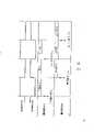
图1为控制器的方块图。Figure 1 is a block diagram of the controller.
图2更详细地表示图1控制器的部分。Figure 2 shows parts of the controller of Figure 1 in more detail.
图3更详细地表示图1控制器的时钟电路。FIG. 3 shows the clock circuit of the controller of FIG. 1 in more detail.
图4更详细地表示用于处理机间通讯的存储器。Figure 4 shows in more detail the memory used for inter-processor communication.
图5表示由时钟电路产生的时钟信号以及微处理机的操作定时。Fig. 5 shows the clock signal generated by the clock circuit and the operation timing of the microprocessor.
图6是用来说明初始化序列的定时程序。Figure 6 is a timing program used to illustrate the initialization sequence.
图7表示控制存储器的机构,并用来说明初始化序列。Figure 7 shows the mechanism for controlling the memory and is used to illustrate the initialization sequence.
在图1所说明的本发明的最佳实施例中,控制器9控制系统母线2和外设1间的数据传递。该控制器9能够控制来自许多不同型号外设1的数据传递,并被设计成用于控制多至16个数据通道的数据传递,其中两个通道并非由外设使用,这样,该控制器能同时控制多至14个外设。In the preferred embodiment of the invention illustrated in FIG. 1, the
该控制器的基本部件包括两个微处理机10和12。它们被联结起来,以便彼此间可以通讯,并且允许共用一个控制存储器14。该控制存储器14由一随机存取存储器(RAM)组成,例如日立(Hitachi)6789。它们也被联结起来以便共用暂存器16,以及允许共用数据缓冲器18X和18Y。在该最佳实施例中,该暂存器16由几个随机存取存储器(RAMs)组成,例如日立(Hitachi)6789和6267P-45,而数据缓冲器是一RAM,例如Hitachi6287。标志为微处理机B的微处理机12控制系统母线2和数据缓冲器18X以及18Y之间的数据传递;而标志为微处理机A的微处理机10控制数据缓冲器18X、18Y和外设1之间的数据传递。这些微处理机10和12的操作由时钟电路38控制。以下将讨论该时钟电路38的细节。The basic components of the controller include two
该控制器可适应不同的系统母线和不同的外设。为适应系统母线或外设的变化,新的固件必须装入控制存储器14。一外设接口20联结在微处理机B和外设1之间,它符合小计算机系统(SCSI)接口规范,(ANSI SPEC.X3.131)。在最佳实施例中,这个接口是一个Western数字3392 SCSI控制器芯片。该外设接口20执行命令、信息、数据,以及状态传递功能。一系列驱动器和接收器3联结到外设接口20,这些驱动器和接收器送信息到外设1或接收来自外设1的信息。同样一接口4提供给系统母线2和控制器的接口。该接口4在上面提及的Barlow等人的申请中作了更充分的描述。The controller can be adapted to different system buses and different peripherals. To accommodate changes in the system bus or peripherals, new firmware must be loaded into the
本发明并不局限于两个微处理机,可以使用两个以上的微处理机,但是至少必须使用两个微处理机。然而,使用两个以上的微处理机无论如何将要求改变同步方法。The present invention is not limited to two microprocessors, more than two microprocessors can be used, but at least two microprocessors must be used. However, the use of more than two microprocessors would require a change in the synchronization method anyway.
图2更详细地表示微处理机A的部件,这些部件包括一指令寄存器22A。用于接收由控制存储器14输入的微指令;还包括解码电路28A,用于对输入的微指令解码。解码单元采用TeXaS测试仪74S138和74S139。同样,在微处理机A中具有一定序器24A。在最佳实施例中,该定序器24A是一种先进的微型器件AMD2910A。该定序器24A控制微处理机的执行顺序。在微处理内还包括一ALU(运算单元)单元31A,当由输入的微指令所控制时,该单元执行计算。该ALU单元31A具有输出寄存器11A,用于在需要输出之前存储其输出。由图2可以看出,微处理机B同样由具有下标B的相同的部件所组成。Figure 2 shows the components of microprocessor A in more detail, these components including an
图3表示时钟电路38的基本部件,而来自该电路的具体的时钟信号在图5中加以说明。该时钟电路包括-20兆周的时钟91,其输出是时钟信号CLKOSC-00。CLKOSC-00馈送到一反相电路88和-D触发器93。它还用于控制器9的其它部件。FIG. 3 shows the basic components of the
CLKOSC-00馈送到D触发器93的时钟信号。该触发器93的置位和复位输入端都处于高电平。由于置位和复位输入端均为低电平有效,所以在典型的操作期间,触发器不置位或复位。D输入端为触发器93的有补输出端CK10MZ-00,无补输出端是CK10MZ+00。CLKOSC-00 feeds clock signal to D flip-flop 93 . Both the set and reset inputs of the flip-flop 93 are at high level. Since the set and reset inputs are active low, the flip-flop does not set or reset during typical operation. The D input terminal is the complementary output terminal CK10MZ-00 of the flip-flop 93, and the non-complementary output terminal is CK10MZ+00.
如上述CLKOSC-00也接至一反相器88,从该反相器88的输出是CLKOSC+00。CLKOSC-00 is also connected to an inverter 88 as above, and the output from this inverter 88 is CLKOSC+00.
D触发器93的CK10MZ+00馈送到另一触发器95。该触发器95属于JK型触发器。CK10MZ+00信号是有补的,并用作JK触发器95的一时钟信号。低电平有效的置位和复位输入端都处于高电平。K输入端也同样处于高电平。J输入端是信号CLKHLT-0X,只在当处于测试方式时,才产生并使用CLKHLT-0X。该信号被用来暂停时钟,而在正常操作期间并不使用。该触发器提供两个输出:CLKSIG+00和它的补码CLKSIG-00,这两个信号都是控制器使用的基本定时信号。CK10MZ+00 of D flip-flop 93 is fed to another flip-flop 95 . This flip-flop 95 belongs to the JK type flip-flop. The CK10MZ+00 signal is complementary and is used as a clock signal for the JK flip-flop 95 . The active-low set and reset inputs are both high. The K input is also at a high level. The J input is the signal CLKHLT-0X, which is generated and used only when in test mode. This signal is used to halt the clock and is not used during normal operation. The flip-flop provides two outputs: CLKSIG+00 and its complement CLKSIG-00, both of which are basic timing signals used by the controller.
为了馈送到JK触发器95,CK10MZ+00信号馈送到两个与非门(NAND)90和92。在第一个与非门90中,CK10MZ+00同CLKSIG+00共同相与非,输出是CLKSTA-00,并由控制器的其它部件所使用。在另一与非门NAND92中,CLKSIG-00同CK10MZ+00共同相与非,产生CLKSTC-00,同样由控制器的其它部件所使用。To feed to JK flip-flop 95 , the CK10MZ+00 signal is fed to two NAND gates (NAND) 90 and 92 . In the first NAND gate 90, CK10MZ+00 is NANDed with CLKSIG+00, and the output is CLKSTA-00, which is used by other parts of the controller. In another NAND gate NAND92, CLKSIG-00 and CK10MZ+00 are NANDed together to generate CLKSTC-00, which is also used by other parts of the controller.
信号CLKOSC+00的补码,对于两个JK触发器96和102而言,起时钟输入作用。JK触发器96具有都处于高电平的J、K和置位输入端,它的复位输入端是CLKSIG-00、该JK触发器96产生两个用于控制器别处的输出:CLKSTB+00以及其补码CLKSTB-00。在另一JK触发器102中,CLKOSC+00用作时钟信号,同样具有其处于高电平的J、K和置位输入端。但复位输入端是不同的。信号是CLKSIG+00,JK触发器的两个输出信号是UPSTB+00和UPSTB-00。The complement of signal CLKOSC+00 serves as the clock input for the two JK flip-flops 96 and 102 . JK flip-flop 96 has J, K, and set inputs all at high levels, and its reset input is CLKSIG-00. This JK flip-flop 96 produces two outputs for use elsewhere in the controller: CLKSTB+00 and Its complement CLKSTB-00. In another JK flip-flop 102 , CLKOSC+00 is used as a clock signal and also has its J, K and set inputs at high level. But the reset input is different. The signal is CLKSIG+00, and the two output signals of the JK flip-flop are UPSTB+00 and UPSTB-00.
图5表示上述所有信号的相互关系。它们在控制器中的控制操作将在下面详细地加以讨论。Figure 5 shows the interrelationship of all the above signals. Their control operation in the controller will be discussed in detail below.
图4表示暂存器16的主要部件。最主要的部件是存储单元30,其它部件包括两个地址寄存器32、34,它们存储来自各微处理机10和12的运算器31A和31B的地址。地址寄存器32和34同多路转接器36一起工作。多路转接器从地址寄存器32和34中的一个选择一个地址。送到存储器单元30的数据输入,以及从存储器单元30输出的数据输出都分别储存在输入寄存器33A和33B以及输出寄存器35A和35B中。FIG. 4 shows the main components of the
控制存储器14包括用于控制每一个微处理机10和12的微指令组。当其中的一个微指令从控制存储器读出时,该指令在下面将要讨论的时刻被闩锁在指令寄存器22A或22B中,为了便于说明,假定它是被记录在指令寄存器22A中。由指令寄存器22保持的不同的微指令位转到解码电路28A。ALU31A,和/或定序器24A。微指令字段,如它的操作码由解码电路28进行解码。
如果该指令要求存取暂存器16,则在暂存器16中的一个地址由ALU31A进行计算。如果要求存取数据缓冲器18X和18Y,则ALU31A也必须计算一个地址。如前所述,定序器24A用微处理机控制微指令的执行次序,它确定下一个将被执行的微指令的地址。在经这些部件的处理之后,微指令的执行就完成了,于是,保持在定序器24A中的下一个微指令地址转到控制存储器14中,这样整个周期将重复。If the instruction requires access to
以上对于微处理机10和12中的一个操作的说明仅孤立地对微处理机进行了描述。因为不论是微处理机10还是12,它们都是共用同个控制存储器14和暂存器16,时钟电路同步上述两者,以便每一个处理机对共用的资源14和16都要进行充分地存取。当考虑需要排除昂贵和低效硬件并防止微处理机之间出现矛盾时,本发明允许这样的共用存取。The foregoing description of the operation of one of the
图5表示用于本发明最佳实施例中的基本定时图。为便于说明,回顾图5所示时钟信号在控制器运行期间如何使用,这将是有帮助的。一个好的起始点就是点55,在该点上,一微指令被记录在微处理机A的指令寄存器22A中。这是使用CLKSIG+00来完成的,只要时钟信号到达指令寄存器22A。如在图5中所能看到的,在CLKSIG+00的高电平部分的前沿处,微指令将被记录在指令寄存器中。指令寄存器22A在实际上至少由三个寄存器22AA,22AB和22AC(图2)组成。每一个寄存器保存三分之一的微指令。Figure 5 shows the basic timing diagram used in the preferred embodiment of the present invention. For purposes of illustration, it is helpful to review how the clock signal shown in Figure 5 is used during controller operation. A good starting point is point 55, at which point a microinstruction is recorded in microprocessor A's
一旦微指令被记录在指令寄存器22A中,微指令二进制位立即被输送到微处理机A的其它单元。因此,在点55到62之间的半个CLKSIG+00周期的时间内,微指令开始执行。如前所述,由指令寄存器22AA,22AB和22AC保持的微指令二进制位输送的地方,由它们代表的字段来确定。这些二进制位输送到解码电路28A,ALU31A,和/或定序器24A。Once the microinstruction is recorded in the
那些输送到解码电路28A的二进制位在它们被解码之前必须等待,直到解码电路被启动为止。解码电路28A由若干解码单元28AA,28AB,28AC,28AD和28AE组成,其中每一个单元都具有各自启动它的时钟信号。这样,当微指令二进制位在CLKSIG+00一周期内被解码时,取决于进入具体解码电路的时钟信号。对指令进行解码以便占据或释放数据缓冲器18的解码电路28AA具有CLKSTC-00的补码作为它的一个启动输入信号。结果,只有在时间期间63才能启动解码单元28AA。同样,将指令进行解码以便写入数据缓冲器的解码单元28AB具有CLKSTA-00的补码作为它的一个启动输入信号。只有在时间期间64才能启动它。还要限制解码单元28AC启动的时间期间,该单元将微指令进行解码,以便由微处理机A写入暂存器16。它的一个启动输入信号是补码CLKSTB-00,它只能在时间期间65被启动。同样,解码单元28AE具有补码CLKSTB-00作为它的一个启动输入信号。Those bits supplied to decoding circuit 28A must wait before they are decoded until the decoding circuit is enabled. Decoding circuit 28A is composed of a number of decoding units 28AA, 28AB, 28AC, 28AD and 28AE, each of which has its own clock signal to activate it. In this way, when the binary bit of the microinstruction is decoded within a period of CLKSIG+00, it depends on the clock signal entering the specific decoding circuit. Decode circuit 28AA, which decodes instructions to occupy or release
如上所述,微指令的二进制位不仅送入解码电路28A,而且还送入ALU31A。这些二进制位用于由ALU31A执行的运算。运算含意取决于已记录在指令寄存器22A中的微指令。ALU31A的输出储存到输出寄存器11A,这些寄存器具有一时钟输入信号OCISTB+00。OCISTB+00为CLKSTB-00的补码和OPCOD1-00的补码相与的结果。OPCOD1-00是由解码单元28AD中的一个所产生的信号。As mentioned above, the binary bits of the microinstructions are sent not only to the decoding circuit 28A, but also to the
这里有四种类型的微指令:置位/复位,ALU,测试与转移以及转移。微指令的前两位数告诉人们该微指令是哪种类型的指令。OPCOD1-00是输出信号,它表示该微指令是一种ALU类型的微指令。OPCODO-00表示一种转移微指令;OPCOD2-00表示一种测试与转移微指令;而OPCOD3-00表示一种置位/复位指令。它们都是低电平有效。这样,对于高电平的OCISTB+00,CLKSTB-00必须是低电平的,以及OPCOD1-00必须是低电平的。There are four types of uops: set/reset, ALU, test and branch, and branch. The first two digits of a uop tell people what type of instruction the uop is. OPCOD1-00 is an output signal indicating that the microinstruction is an ALU type microinstruction. OPCODO-00 represents a transfer microinstruction; OPCOD2-00 represents a test and transfer microinstruction; and OPCOD3-00 represents a set/reset instruction. They are all active low. Thus, for OCISTB+00 to be high, CLKSTB-00 must be low, and OPCOD1-00 must be low.
上面还提到二进制位进到定序器24A。该定序器24A,像指令寄存器22A那样,使用CLKSIG+00作为它的时钟信号。在CLKSIG+00信号的上升沿,来自ALU31A以及解码电路28A的字段都记录到定序器24A中,但是不能输出,直到UPRCEN-OA为高电平。UPRCEN-OA是与非门119的输出,该与非门119具有输入信号:CLKSIG-00和UPRCEN+00(一测试信号;在正常运行期间处高电平)。在正常运行期间,UPRCEN-OA受CLKSIG-00的控制。这样,字段将在点55记录到定序器24A。微处理机B具有相应的信号UPRCEN+OB和CLKSIG+00。在正常运行期间UPRCEN+OB处于高电平。UPRCEN-OB是来自具有输入信号CLKSIG+00和UPRCEN+OB的与非门118的输出。在点62之前,定序器24A最后所得到的输出是无效的。在点60,该微指令数据被记录到指令寄存器22A。It was also mentioned above that the bits go to sequencer 24A. The sequencer 24A, like the
由定序器24A产生的地址在点62送到控制存储器的开关部分。该地址在点62开始的半周期内用来检索来自控制存储器14的微指令。该检索到的微指令,在点60之前并不记录到指令寄存器22A。截止到点60,完成执行上述取微指令的程序。在点60,对于微处理机A,周期重新开始。The address generated by sequencer 24A is sent at point 62 to the switch portion of the control memory. This address is used to retrieve microinstructions from
以上讨论说明,包括在最佳实施例中的同步操作。在点62,微处理机B具有记录在它的指令寄存器22B内的微指令。它重复以上对微处理机A所描述的步骤,但是微处理机B运行在同微处理机A异相的CLKSIG+00的半周期。微处理机间定时差异可以从对每一个微处理机的时钟信号上看出来。开始时,到微处理机B的指令寄存器的时钟信号为CLKSIG-00,进而,解码单元利用不同的时钟电路。负责用于对要求暂存器存取的微指令进行解码的解码单元28BC和28BE用UPSTB-00补码作为它们的时钟信号。对微指令进行解码,以便释放或占所据数据缓冲器18X和18Y的解码电路28BA,用CLKSTA-00的补码作为它的时钟信号。此外,对指令进行解码,以便写入数据缓冲器的解码单元28BB,用CLKSTC-00的补码为它的时钟输入。The above discussion illustrates, including synchronous operation in the preferred embodiment. At point 62, microprocessor B has the microinstruction recorded in its
由于这些时钟信号作用的结果,在时间期间67,对于在点58和62之间的CLKSIG-00的一段时间,数据缓冲器只可以被微处理机B占据或释放。同样,由微处理机B写入暂存器被限制在时间期间66,而写入数据缓冲器被限制在时间期间68。同步电路既允许微处理机10,也允许微处理机12充分地共用暂存器16,控制存储器14,以及数据缓冲器18X和18Y而不出现矛盾。As a result of these clock signals, the data buffer can only be occupied or released by microprocessor B during time period 67 for a period of CLKSIG-00 between points 58 and 62. Likewise, writing to the scratchpad by microprocessor B is limited to a time period 66 and writing to the data buffer is limited to a time period 68 . The synchronization circuit allows both
每一个微处理机10和12的定序器24A和24B也依赖不同的时钟信号。如前所术,CLKSIG+00是用于定序器24B的时钟信号。此外,定序器24A依靠CLKSIG-00作为它的输出允许。另一方面,定序器24B依靠CLKSIG+00作为它的输出允许。The sequencers 24A and 24B of each
当检查了微处理机的字段在何处送到指令寄存器22A之后,有必要进一步观察解码电路28A的输出。如果要求数据缓冲器占据或释放的一微指令被解码,则解码单元适当的输出被转到在程序阵列逻辑(PLA)中实现的占据逻辑19。在最佳实施例中,使用PAL20R4A和PAL20L8A芯片。占据逻辑19确定一数据缓冲器是否被微处理机10和12中的一个所占据。PAL19联到多路转接器27和29。这些多路转接器用于选择地址寄存器23和25的一个地址。它们由信号CLKSIG+11定时,该信号通过一反相器120由取补CLKSIG+00得到的。然而,数据缓冲器18X和18Y不是本发明的中心点。这样,在有关的具有页式数据缓冲管理的外设控制器的申请中将对数据缓冲器和占据逻辑作更为详尽地说明。After examining where the microprocessor fields are sent to the
如果由解码电路28A解码的微指令试图存取暂存器16,该解码电路28A的适当的信号将送到该暂存器16。有两个信号是特别感兴趣的:SPMIDA-00和SRIA02-00。信号SPMIDA-00来自解码器28AC,并指示要求一个指令,以便使保持在暂存器地址寄存器32中的地址为增量地址。信号SRIA02-00指示该暂存器地址寄存器32用微指令的AOP字段加载。该AOP字段由微指令的第7到第10位组成。这两个信号特别有趣,是因为它们的补码相或产生SPMCLK+00。SPMCLK+00用作地址寄存器32的输入时钟信号。If a microinstruction decoded by decoding circuit 28A attempts to access
在暂存器16中存取的地址由ALU31A进行运算,运算后的地址在SPMCLK+00的高电平部分的前沿记入暂存器地址寄存器32。但是在多路转接器36选择那个地址寄存器32之前,该地址是不使用的。它选择哪一个地址寄存器,这将取决于CLKSIG+00的状态。如果CLKSIG+00是高电平,则多路转换器将选择地址寄存器32,相反,如果CLKSIG+00是低电平,将选择地址寄存器34。这样,在接着半周期的半周期时间里,地址装入地址寄存器32和34之前,多路转接器36不作选择。例如,在62和60之间的半个周期期间,地址寄存器32会接受一个地址。但是直到紧接60的半周期为止,在存储单元30中由地址表示的存储器位置不能加以存取。一旦进行选择,在地址寄存器中的地址被用于存取存储单元30。The address accessed in the
所有对存储单元30的输入均储存在输入寄存器33A和33B中。寄存器33A储存微处理机A的输入,而33B储存微处理机B的输入。输入寄存器33A和33B的时钟信号总是处于高电平,因此,它们的同步由它们的输出启动控制。它们的输出分别由SPMWEN-OA的补码和SPMWEN-OB的补码启动。SPMWEN-OA和SPMWEN-OB取自多路转接器121。如果CLKSIG+00为高电平,和SPMWRT-OA为高电平,则SPMWEN-OA为低电平,并且启动输出来自输入寄存器33A。同样,如果CLKSIG-00为低电平,而SPMWRT-OB为高电平,则SPMWEN-OB为低电平,并且启动输出来自输入寄存器33B,输出被储存在输出寄存器35A和35B中。35A储存用于微处理机A的输出,而35B储存用于微处理机B的输出。输出寄存器35A用CLKSIG+00作为它的时钟信号,而输出寄存器35B用CLKSIG-00作为它的时钟信号,这样,两个输出寄存器35A和35B是半个周期异相。All inputs to
为了说明,以上讨论集中在微处理机A。应当指出,微处理机B的运行是类同的。两个微处理机10和12之间的差别在于控制它们运行的定时信号。在多数场合中,对于在讨论微处理机A时的每一个信号,对微处理机B存在相应的信号。以上对主要相应信号已作出讨论。For purposes of illustration, the above discussion has focused on microprocessor A. It should be noted that the operation of microprocessor B is similar. The difference between the two
以上对定时的说明乃是为了直观的解说目的。微处理机A和微处理B能够以不同于所描述的方案进行同步(即微处理机A和微处理机B,在当它们执行给定任务时能够交换次序(Swap times))。再者,若使用两个以上的微处理机,则不得不改变定时。例如使用三个微处理机,则一个周期将分成三个部分,而在各自的时间期间内,每一部分执行自己的操作。这些变化也包括在本发明之内。The above description of the timing is for the purpose of intuitive explanation. Microprocessor A and microprocessor B can synchronize in a different scheme than that described (ie, microprocessor A and microprocessor B can swap times when they perform a given task). Furthermore, if more than two microprocessors are used, the timing has to be changed. Using three microprocessors, for example, a cycle would be divided into three parts, with each part performing its own operation during its own time period. These changes are also included in the present invention.
为了利用本发明的控制存储器14,它必须首先作操作准备。准备工作包括把测试微指令装入控制存储器14的初始位置50(见图7)。每一个微处理机10和12的微指令组52和54也分别装入控制存储器14。它们可以组织成像图7那样的结构形式,或者也可组织成别的形式。如果有这种要求的话。当微处理机10和12开始运行时,它们被指向储存测试微指令的初始位置50。In order to utilize the
该测试微指令包括测试与转移型的微指令。测试微指令测试微处理机执行的测试微指令的全同性。测试微指令了解微处理机中的一个微处理机的全同性。例如,假定它了解微处理机A的全同性,它用已知的全同性来比较执行测试微指令的微处理机的全同性。如果同一性与已知的同一性相符,则产生转移。因此,当执行测试微指令时,其同一性与已知的同一性相符的微处理机A将转移到它的微指令组52的起点。相反,当微处理机B执行测试微指令时,同一性不符合,因此,它就不能转移。按顺序的下一个微指令:微处理机B的一组微指令54的起点将被取出。The test microinstructions include test and branch microinstructions. The test microinstructions test the identity of the test microinstructions executed by the microprocessor. Test microinstructions for identity of one of the microprocessors. For example, assuming it knows the identity of microprocessor A, it uses the known identity to compare the identity of the microprocessor executing the test microinstruction. If the identity matches known identities, transfer occurs. Thus, when executing the test microinstruction, microprocessor A whose identity matches the known identity will branch to the beginning of its
图6表示定时处理过程,在点5,测试指令记录到微处理机A,在紧接点5的半个周期期间,按测试指令开始执行指令。在点6,测试微指令记录到微处理机B,在紧接点6的半个周期期间,微处理机A将转移。微处理机B开始执行测试指令。在点7,用于微处理机A的一组微指令52的第一个微指令将记录到微处理机A。对于微处理机A的处理在前面已加以描述。在紧接点7的半周期期间,微处理机B将完成测试指令的执行,并且在点8装入一组微指令54的第一个指令。在点8之后,对于微处理机B的处理在前面已加以描述。FIG. 6 shows the timing process. At point 5, the test instruction is recorded into microprocessor A. During the half cycle immediately following point 5, execution of the instruction is started according to the test instruction. At point 6, the test uop is logged into microprocessor B, and during the half cycle immediately following point 6, microprocessor A will branch. Microprocessor B starts to execute the test instruction. At point 7, the first microinstruction of the set of
本发明提供了若干优点,这些优点改善了系统性能而优于现有技术。首先它不要求昂贵和累赘的硬件去同步微处理机,其次它比现有技术的效率高,因为它共用数据缓冲器,暂存器和一个控制存储器。这里并不需要单独的数据缓冲器,暂存器,而特别是不需要单独的用于每一个微处理机的控制存储器。第三,提供了同步,伪的或视在的同时读/写能力。所有这些都是优点。应当理解的是,这些例举的优点并不是详尽无遗的。The present invention provides several advantages which improve system performance over the prior art. Firstly it does not require expensive and cumbersome hardware to synchronize the microprocessor, and secondly it is more efficient than the prior art because it shares data buffers, scratchpads and a control memory. There is no need for separate data buffers, temporary registers, and especially no separate control memory for each microprocessor. Third, synchronous, pseudo or apparent simultaneous read/write capability is provided. All of these are advantages. It should be understood that these enumerated advantages are not exhaustive.
当对照一最佳实施例具体地指明并描述了本发明的时候,本专业技术人员将理解在不超出由附加权利要求所限制的本发明的精神和范围内可以做出形式和细节上的不同的改变。While the present invention has been particularly shown and described with reference to a preferred embodiment, those skilled in the art will understand that changes may be made in form and details without departing from the spirit and scope of the invention as defined by the appended claims. change.
Claims (14)
Translated fromChineseApplications Claiming Priority (2)
| Application Number | Priority Date | Filing Date | Title |
|---|---|---|---|
| US07/295,629US5081609A (en) | 1989-01-10 | 1989-01-10 | Multiprocessor controller having time shared control store |
| US07/295,629 | 1989-01-10 |
Publications (2)
| Publication Number | Publication Date |
|---|---|
| CN1044720Atrue CN1044720A (en) | 1990-08-15 |
| CN1021147C CN1021147C (en) | 1993-06-09 |
Family
ID=23138542
Family Applications (1)
| Application Number | Title | Priority Date | Filing Date |
|---|---|---|---|
| CN90100762AExpired - Fee RelatedCN1021147C (en) | 1989-01-10 | 1990-01-10 | Multiprocessor controller with shared control memory |
Country Status (9)
| Country | Link |
|---|---|
| US (1) | US5081609A (en) |
| EP (1) | EP0378071B1 (en) |
| JP (1) | JPH02226457A (en) |
| KR (1) | KR940011594B1 (en) |
| CN (1) | CN1021147C (en) |
| AU (1) | AU622748B2 (en) |
| CA (1) | CA2007004C (en) |
| DE (1) | DE69032511T2 (en) |
| NO (1) | NO900093L (en) |
Cited By (1)
| Publication number | Priority date | Publication date | Assignee | Title |
|---|---|---|---|---|
| CN100409221C (en)* | 2002-12-05 | 2008-08-06 | 亮标公司 | Data processing system with Cartesian controller and method of processing data |
Families Citing this family (11)
| Publication number | Priority date | Publication date | Assignee | Title |
|---|---|---|---|---|
| US5347638A (en)* | 1991-04-15 | 1994-09-13 | Seagate Technology, Inc. | Method and apparatus for reloading microinstruction code to a SCSI sequencer |
| NL9301129A (en)* | 1993-06-29 | 1995-01-16 | Nederland Ptt | Processor circuit comprising a first processor, and system comprising the processor circuit and a second processor. |
| US9513744B2 (en)* | 1994-08-15 | 2016-12-06 | Apple Inc. | Control systems employing novel physical controls and touch screens |
| US5564027A (en)* | 1995-04-20 | 1996-10-08 | International Business Machines Corporation | Low latency cadence selectable interface for data transfers between busses of differing frequencies |
| KR960043938A (en)* | 1995-05-27 | 1996-12-23 | 김광호 | Message Overload Control Method for Unit Program of Multiprocessor Control System |
| US20090273574A1 (en)* | 1995-06-29 | 2009-11-05 | Pryor Timothy R | Programmable tactile touch screen displays and man-machine interfaces for improved vehicle instrumentation and telematics |
| US5644174A (en)* | 1996-03-22 | 1997-07-01 | Sun Microsystems, Inc. | Universal AC sequencer for a server |
| CA2299550A1 (en)* | 1999-03-31 | 2000-09-30 | International Business Machines Corporation | Dynamic i/o allocation in a partitioned computer system |
| US20080129707A1 (en)* | 2004-07-27 | 2008-06-05 | Pryor Timothy R | Method and apparatus employing multi-functional controls and displays |
| US20100231506A1 (en)* | 2004-09-07 | 2010-09-16 | Timothy Pryor | Control of appliances, kitchen and home |
| WO2011002371A1 (en)* | 2009-07-03 | 2011-01-06 | Axel Jantsch | A programmable controller |
Family Cites Families (37)
| Publication number | Priority date | Publication date | Assignee | Title |
|---|---|---|---|---|
| US3500466A (en)* | 1967-09-11 | 1970-03-10 | Honeywell Inc | Communication multiplexing apparatus |
| US3651482A (en)* | 1968-04-03 | 1972-03-21 | Honeywell Inc | Interlocking data subprocessors |
| IT991096B (en)* | 1973-07-10 | 1975-07-30 | Honeywell Inf Systems | ELECTRONIC CALCULATOR WITH INDEPENDENT FUNCTIONAL NETWORKS FOR THE SIMULTANEOUS EXECUTION OF DIFFERENT OPERATIONS ON THE SAME DATA |
| JPS5410219B2 (en)* | 1973-12-07 | 1979-05-02 | ||
| US3909799A (en)* | 1973-12-18 | 1975-09-30 | Honeywell Inf Systems | Microprogrammable peripheral processing system |
| JPS5194734A (en)* | 1975-02-19 | 1976-08-19 | Tajushorisochino enzanseigyohoshiki | |
| US4028668A (en)* | 1975-12-22 | 1977-06-07 | Honeywell Information Systems, Inc. | Apparatus for selectively addressing sections and locations in a device controller's memory |
| US4124888A (en)* | 1975-12-24 | 1978-11-07 | Computer Automation, Inc. | Peripheral-unit controller apparatus |
| US4084229A (en)* | 1975-12-29 | 1978-04-11 | Honeywell Information Systems Inc. | Control store system and method for storing selectively microinstructions and scratchpad information |
| US4062058A (en)* | 1976-02-13 | 1977-12-06 | The United States Of America As Represented By The Secretary Of The Navy | Next address subprocessor |
| US4156925A (en)* | 1976-04-30 | 1979-05-29 | International Business Machines Corporation | Overlapped and interleaved control store with address modifiers |
| US4050097A (en)* | 1976-09-27 | 1977-09-20 | Honeywell Information Systems, Inc. | Synchronization technique for data transfers over an asynchronous common bus network coupling data processing apparatus |
| US4085450A (en)* | 1976-12-29 | 1978-04-18 | Burroughs Corporation | Performance invarient execution unit for non-communicative instructions |
| US4296464A (en)* | 1977-03-03 | 1981-10-20 | Honeywell Inc. | Process control system with local microprocessor control means |
| JPS5440537A (en)* | 1977-09-07 | 1979-03-30 | Hitachi Ltd | Pipeline control system |
| US4246637A (en)* | 1978-06-26 | 1981-01-20 | International Business Machines Corporation | Data processor input/output controller |
| US4321665A (en)* | 1979-01-31 | 1982-03-23 | Honeywell Information Systems Inc. | Data processing system having centralized data alignment for I/O controllers |
| US4327408A (en)* | 1979-04-17 | 1982-04-27 | Data General Corporation | Controller device with diagnostic capability for use in interfacing a central processing unit with a peripheral storage device |
| US4371932A (en)* | 1979-07-30 | 1983-02-01 | International Business Machines Corp. | I/O Controller for transferring data between a host processor and multiple I/O units |
| US4322792A (en)* | 1979-12-14 | 1982-03-30 | Burroughs Corporation | Common front-end control for a peripheral controller connected to a computer |
| US4323967A (en)* | 1980-04-15 | 1982-04-06 | Honeywell Information Systems Inc. | Local bus interface for controlling information transfers between units in a central subsystem |
| US4348723A (en)* | 1980-04-15 | 1982-09-07 | Honeywell Information Systems Inc. | Control store test selection logic for a data processing system |
| US4488231A (en)* | 1980-09-29 | 1984-12-11 | Honeywell Information Systems Inc. | Communication multiplexer having dual microprocessors |
| US4384285A (en)* | 1981-02-19 | 1983-05-17 | Honeywell Information Systems Inc. | Data character video display system with visual attributes |
| US4603400A (en)* | 1982-09-30 | 1986-07-29 | Pitney Bowes Inc. | Mailing system interface interprocessor communications channel |
| WO1984003192A1 (en)* | 1983-02-07 | 1984-08-16 | American Telephone & Telegraph | Data network interface |
| JPS60122450A (en)* | 1983-12-05 | 1985-06-29 | Hitachi Ltd | Microprocessor |
| US4695943A (en)* | 1984-09-27 | 1987-09-22 | Honeywell Information Systems Inc. | Multiprocessor shared pipeline cache memory with split cycle and concurrent utilization |
| US4800523A (en)* | 1985-02-25 | 1989-01-24 | Itt Corporation | Device interface controller having device specific and device common instructions separately stored |
| US4750113A (en)* | 1985-02-28 | 1988-06-07 | Unisys Corporation | Dual function I/O controller |
| US4754396A (en)* | 1986-03-28 | 1988-06-28 | Tandem Computers Incorporated | Overlapped control store |
| US5010476A (en)* | 1986-06-20 | 1991-04-23 | International Business Machines Corporation | Time multiplexed system for tightly coupling pipelined processors to separate shared instruction and data storage units |
| US4890218A (en)* | 1986-07-02 | 1989-12-26 | Raytheon Company | Variable length instruction decoding apparatus having cross coupled first and second microengines |
| JPS63228250A (en)* | 1987-03-17 | 1988-09-22 | Fujitsu Ltd | input/output control device |
| US4821170A (en)* | 1987-04-17 | 1989-04-11 | Tandem Computers Incorporated | Input/output system for multiprocessors |
| US4890225A (en)* | 1988-04-01 | 1989-12-26 | Digital Equipment Corporation | Method and apparatus for branching on the previous state in an interleaved computer program |
| US5117387A (en)* | 1988-08-18 | 1992-05-26 | Delco Electronics Corporation | Microprogrammed timer processor |
- 1989
- 1989-01-10USUS07/295,629patent/US5081609A/ennot_activeExpired - Lifetime
- 1990
- 1990-01-02CACA002007004Apatent/CA2007004C/ennot_activeExpired - Fee Related
- 1990-01-02EPEP90100022Apatent/EP0378071B1/ennot_activeExpired - Lifetime
- 1990-01-02DEDE69032511Tpatent/DE69032511T2/ennot_activeExpired - Fee Related
- 1990-01-05AUAU47722/90Apatent/AU622748B2/ennot_activeCeased
- 1990-01-08KRKR1019900000123Apatent/KR940011594B1/ennot_activeExpired - Fee Related
- 1990-01-09NONO90900093Apatent/NO900093L/enunknown
- 1990-01-10CNCN90100762Apatent/CN1021147C/ennot_activeExpired - Fee Related
- 1990-01-10JPJP2003289Apatent/JPH02226457A/enactivePending
Cited By (1)
| Publication number | Priority date | Publication date | Assignee | Title |
|---|---|---|---|---|
| CN100409221C (en)* | 2002-12-05 | 2008-08-06 | 亮标公司 | Data processing system with Cartesian controller and method of processing data |
Also Published As
| Publication number | Publication date |
|---|---|
| NO900093L (en) | 1990-07-11 |
| AU622748B2 (en) | 1992-04-16 |
| CA2007004A1 (en) | 1990-07-10 |
| KR940011594B1 (en) | 1994-12-22 |
| CN1021147C (en) | 1993-06-09 |
| JPH02226457A (en) | 1990-09-10 |
| KR900012156A (en) | 1990-08-03 |
| NO900093D0 (en) | 1990-01-09 |
| EP0378071A2 (en) | 1990-07-18 |
| CA2007004C (en) | 1994-06-07 |
| AU4772290A (en) | 1990-07-19 |
| US5081609A (en) | 1992-01-14 |
| EP0378071B1 (en) | 1998-07-29 |
| DE69032511T2 (en) | 1999-04-29 |
| EP0378071A3 (en) | 1991-08-28 |
| DE69032511D1 (en) | 1998-09-03 |
Similar Documents
| Publication | Publication Date | Title |
|---|---|---|
| CN1113300C (en) | Semiconductor device and computer system | |
| US5459843A (en) | RISC-type pipeline processor having N slower execution units operating in parallel interleaved and phase offset manner with a faster fetch unit and a faster decoder | |
| US5664214A (en) | Parallel processing computer containing a multiple instruction stream processing architecture | |
| US5235686A (en) | Computer system having mixed macrocode and microcode | |
| US4181974A (en) | System providing multiple outstanding information requests | |
| US5960458A (en) | Shared memory system | |
| CN1021147C (en) | Multiprocessor controller with shared control memory | |
| CN1211012A (en) | Method and apparatus for interfacing a processor with a coprocessor | |
| JPS6258028B2 (en) | ||
| JPH11296389A (en) | Context controller for managing multi-tasking by processor | |
| US4236203A (en) | System providing multiple fetch bus cycle operation | |
| US5655131A (en) | SIMD architecture for connection to host processor's bus | |
| US7197590B2 (en) | Method and apparatus for connecting LPC bus and serial flash memory | |
| JPH08166902A (en) | Integrated-circuit microprocessor provided with programmablememory access interface type and related method | |
| JPS58222363A (en) | Distributor for common memory | |
| JPS6319854Y2 (en) | ||
| JPS62272343A (en) | Fast decentralized control memory system and method thereof | |
| US4245299A (en) | System providing adaptive response in information requesting unit | |
| GB2060961A (en) | Data processing system having memory modules with distributed address information | |
| JPS6333177B2 (en) | ||
| JPH11296385A (en) | Context controller for managing multi-tasking by processor | |
| CN1008667B (en) | Apparatus for outputting micro-commands for pipeline execution by a microprogram control data system | |
| EP0376003A2 (en) | Multiprocessing system with interprocessor communications facility | |
| JPS6217777B2 (en) | ||
| JP2763655B2 (en) | Semiconductor integrated circuit |
Legal Events
| Date | Code | Title | Description |
|---|---|---|---|
| C06 | Publication | ||
| PB01 | Publication | ||
| C10 | Entry into substantive examination | ||
| SE01 | Entry into force of request for substantive examination | ||
| C14 | Grant of patent or utility model | ||
| GR01 | Patent grant | ||
| C19 | Lapse of patent right due to non-payment of the annual fee | ||
| CF01 | Termination of patent right due to non-payment of annual fee |