CN103907051A - Manufacturing system of optical display device and manufacturing method - Google Patents
Manufacturing system of optical display device and manufacturing methodDownload PDFInfo
- Publication number
- CN103907051A CN103907051ACN201280053622.XACN201280053622ACN103907051ACN 103907051 ACN103907051 ACN 103907051ACN 201280053622 ACN201280053622 ACN 201280053622ACN 103907051 ACN103907051 ACN 103907051A
- Authority
- CN
- China
- Prior art keywords
- optical member
- sheet
- bonding
- optical
- primary
- Prior art date
- Legal status (The legal status is an assumption and is not a legal conclusion. Google has not performed a legal analysis and makes no representation as to the accuracy of the status listed.)
- Granted
Links
Images


Classifications
- G—PHYSICS
- G02—OPTICS
- G02F—OPTICAL DEVICES OR ARRANGEMENTS FOR THE CONTROL OF LIGHT BY MODIFICATION OF THE OPTICAL PROPERTIES OF THE MEDIA OF THE ELEMENTS INVOLVED THEREIN; NON-LINEAR OPTICS; FREQUENCY-CHANGING OF LIGHT; OPTICAL LOGIC ELEMENTS; OPTICAL ANALOGUE/DIGITAL CONVERTERS
- G02F1/00—Devices or arrangements for the control of the intensity, colour, phase, polarisation or direction of light arriving from an independent light source, e.g. switching, gating or modulating; Non-linear optics
- G02F1/01—Devices or arrangements for the control of the intensity, colour, phase, polarisation or direction of light arriving from an independent light source, e.g. switching, gating or modulating; Non-linear optics for the control of the intensity, phase, polarisation or colour
- G02F1/13—Devices or arrangements for the control of the intensity, colour, phase, polarisation or direction of light arriving from an independent light source, e.g. switching, gating or modulating; Non-linear optics for the control of the intensity, phase, polarisation or colour based on liquid crystals, e.g. single liquid crystal display cells
- G02F1/1303—Apparatus specially adapted to the manufacture of LCDs
Landscapes
- Physics & Mathematics (AREA)
- Nonlinear Science (AREA)
- Engineering & Computer Science (AREA)
- Manufacturing & Machinery (AREA)
- Chemical & Material Sciences (AREA)
- Crystallography & Structural Chemistry (AREA)
- General Physics & Mathematics (AREA)
- Optics & Photonics (AREA)
- Liquid Crystal (AREA)
- Polarising Elements (AREA)
- Devices For Indicating Variable Information By Combining Individual Elements (AREA)
Abstract
Translated fromChineseDescription
Translated fromChinese技术领域technical field
本发明涉及一种液晶显示器等的光学显示设备的生产系统以及生产方法。The present invention relates to a production system and production method of optical display devices such as liquid crystal displays.
本发明基于2011年11月30日提出的特愿2011-262949号申请以及在2011年11月30日提出的特愿2011-262950号申请主张优先权,在此引用其中内容。The present invention claims priority based on Japanese Patent Application No. 2011-262949 filed on November 30, 2011 and Japanese Patent Application No. 2011-262950 filed on November 30, 2011, the contents of which are incorporated herein.
背景技术Background technique
以往,在液晶显示器等的光学显示设备的生产系统中,存在贴合在液晶面板(光学显示零件)的偏振片等光学构件从长条膜被切割成符合液晶面板的显示区域的尺寸的片材,被包装并被输送到别的生产线后,被贴合到液晶面板上的情况(例如,参照专利文献1)。Conventionally, in the production system of optical display devices such as liquid crystal displays, optical members such as polarizers bonded to liquid crystal panels (optical display components) are cut from long films into sheets of the size corresponding to the display area of the liquid crystal panel. , is packaged and transported to another production line, and then bonded to a liquid crystal panel (for example, refer to Patent Document 1).
现有技术文献prior art literature
专利文献patent documents
专利文献1日本特开2003-255132号公报Patent Document 1 Japanese Patent Laid-Open No. 2003-255132
发明内容Contents of the invention
发明要解决的课题The problem to be solved by the invention
但是,在上述现有的结构中,考虑液晶面板以及片材的各尺寸参差不齐,以及片材相对于液晶面板的贴合参差不齐(位置偏差),切出比显示区域略大的片材。因此,具有在显示区域的周边部形成多余的区域(框缘部),阻碍设备的小型化的问题。However, in the above-mentioned conventional structure, the size of the liquid crystal panel and the sheet is uneven, and the bonding of the sheet to the liquid crystal panel is uneven (positional deviation), and a sheet slightly larger than the display area is cut out. material. Therefore, there is a problem that a redundant area (frame portion) is formed in the peripheral portion of the display area, which hinders miniaturization of the device.
又,将光学构件贴合在液晶面板之前,通过液晶面板的静电去除等抑制尘土附着在液晶面板上,但还具有以下这样的问题:由于被贴合在液晶面板的光学构件的贴合面具有粘着性,因此容易附着尘土,成为导致贴合不良发生的一个原因。Again, before the optical member is bonded to the liquid crystal panel, dust is suppressed from adhering to the liquid crystal panel by static electricity removal of the liquid crystal panel, etc., but there is also the following problem: since the bonding surface of the optical member bonded to the liquid crystal panel has Since it is sticky, dust is easy to adhere to, which becomes one of the causes of poor bonding.
本发明正视鉴于上述情况而做出的,其提供一种能够缩小显示区域周边的框部,谋求显示区域的扩大以及设备的小型化,并且抑制尘土附着在光学构件的贴合面的光学显示设备的生产系统以及生产方法。The present invention is made in view of the above situation, and it provides an optical display device capable of reducing the frame portion around the display area, expanding the display area and reducing the size of the device, and suppressing dust from adhering to the bonding surface of the optical member. production systems and production methods.
为了解决上述课题,本发明具有以下的方式。In order to solve the above-mentioned problems, the present invention has the following aspects.
本发明的第一方式的光学显示设备的生产系统是将光学构件贴合在光学显示零件上而形成的光学显示设备的生产系统,其具有:一次贴合装置,所述一次贴合装置对于在生产线上输送的多个所述光学显示零件,边从一次卷材放卷带状的一次光学构件片,边将多个所述光学显示零件的第一面贴合在所述一次光学构件片上形成贴合片,所述一次光学构件片在与所述光学显示零件的输送方向正交的零件宽度方向具有比所述光学显示零件的显示区域的宽度大的宽度;一次切割装置,所述一次切割装置通过将与所述显示区域相对的所述一次光学构件片的相对部分和位于所述相对部分的外侧的剩余部分切割开,并从所述一次光学构件片切割出作为具有与所述显示区域对应的大小的所述光学构件的一次光学构件,从而从所述贴合片切割出一次光学构件贴合体,所述一次光学构件贴合体包括单一的光学显示零件以及与所述单一的光学显示零件重叠的所述一次光学构件;以及二次贴合装置,所述二次贴合装置对于在生产线上输送的多个所述一次光学构件贴合体,将在所述零件宽度方向上具有与所述显示区域对应的宽度的带状的二次光学构件片和隔片一起从二次卷材放卷,每次以与所述显示区域对应的长度放卷所述二次光学构件片,就在所述二次光学构件片上实施沿着宽度方向的切割,形成作为具有与所述显示区域对应的大小的所述光学构件的二次光学构件之后,一边将所述隔片作为载体输送多个所述二次光学构件,一边将所述二次光学构件贴合于所述一次光学构件贴合体中的所述光学显示零件的第二面。The production system of an optical display device according to the first aspect of the present invention is a production system of an optical display device formed by bonding an optical member to an optical display component, and includes: a primary bonding device for The plurality of optical display components conveyed on the production line are formed by bonding the first surfaces of the plurality of optical display components to the primary optical member sheet while unwinding the strip-shaped primary optical member sheet from the primary roll. The bonding sheet, the primary optical member sheet has a width larger than the width of the display area of the optical display part in the part width direction perpendicular to the conveying direction of the optical display part; the primary cutting device, the primary cutting The device is formed by cutting the opposite part of the primary optical member sheet opposite to the display area and the remaining part located outside the opposite part, and cutting out from the primary optical member sheet as a The primary optical member of the optical member of the corresponding size, thereby cutting out the primary optical member bonded body from the bonding sheet, the primary optical member bonded body includes a single optical display part and the single optical display part The overlapping primary optical member; and a secondary bonding device, for a plurality of the primary optical member bonding bodies conveyed on the production line, the The strip-shaped secondary optical member sheet with a width corresponding to the display area is unwound from the secondary coil together with the spacer, and the secondary optical member sheet is unwound with the length corresponding to the display area each time, and the Cutting along the width direction is performed on the secondary optical member sheet to form a secondary optical member having a size corresponding to the display area, and transporting a plurality of the secondary optical members while using the spacer as a carrier. The secondary optical member is bonded to the second surface of the optical display component in the bonded body of the primary optical member.
另外,上述结构中的“相对部分”表示具有显示区域的大小以上、光学显示零件的外部形状的大小以下的大小,且避开了电气零件安装部等功能部分的区域。即,上述结构包含沿光学显示零件的外周缘激光切割剩余部分的情况。In addition, the "opposite part" in the above structure means a region having a size greater than or equal to the size of the display area and less than or equal to the size of the external shape of the optical display component, and avoiding functional parts such as electrical component mounting parts. That is, the above structure includes the case of laser cutting the remaining portion along the outer peripheral edge of the optical display part.
在本发明的一实施方式的光学显示设备的生产系统中,优选为,所述二次贴合装置具有:放卷部,所述放卷部将所述二次光学构件片和所述隔片一起放卷;切割部,所述切割部对所述二次光学构件片实施切割并形成所述二次光学构件;检测部,所述检测部在与对所述二次光学构件片实施切割的切割位置相比,在所述二次光学构件片的放卷方向上向下游侧隔开与一个所述二次光学构件大小对应的距离的位置,对通过所述切割形成在所述二次光学构件片上的切割线进行检测;以及控制部,在从所述切割位置向所述下游侧隔开一个所述二次光学构件大小的距离的检测位置检测到所述切割线时,所述控制部根据所述切割线的位置对所述切割位置和所述检测位置之间的距离进行调整。In the production system of an optical display device according to an embodiment of the present invention, it is preferable that the secondary laminating device has: an unwinding part that holds the secondary optical member sheet and the spacer unwinding together; the cutting part, the cutting part cuts the secondary optical member sheet and forms the secondary optical member; the detection part, the detection part performs cutting on the secondary optical member sheet Compared with the cutting position, the position separated from the downstream side in the unwinding direction of the secondary optical member sheet by a distance corresponding to the size of one secondary optical member is formed on the secondary optical member by the cutting. The cutting line on the component sheet is detected; and the control unit detects the cutting line at a detection position separated from the cutting position to the downstream side by a distance of the size of the secondary optical member. The distance between the cutting position and the detection position is adjusted according to the position of the cutting line.
本发明的第二方式的光学显示设备的生产方法是将光学构件贴合在光学显示零件上而形成的光学显示设备的生产方法,对于在生产线上输送的多个所述光学显示零件,边从一次卷材放卷带状的一次光学构件片,边将多个所述光学显示零件的第一面贴合在所述一次光学构件片上形成贴合片,所述一次光学构件片在与所述光学显示零件的输送方向正交的零件宽度方向具有比所述光学显示零件的显示区域的宽度大的宽度,通过将与所述显示区域相对的所述一次光学构件片的相对部分和位于所述相对部分的外侧的剩余部分切割开,并从所述一次光学构件片切割出作为具有与所述显示区域对应的大小的所述光学构件的一次光学构件,从而从所述贴合片切割出一次光学构件贴合体,所述一次光学构件贴合体包括单一的光学显示零件以及与所述单一的光学显示零件重叠的所述一次光学构件,对于在生产线上输送的多个所述一次光学构件贴合体,将在所述零件宽度方向上具有与所述显示区域对应的宽度的带状的二次光学构件片和隔片一起从二次卷材放卷,每次以与所述显示区域对应的长度放卷所述二次光学构件片,就在所述二次光学构件片上实施沿着宽度方向的切割,形成作为具有与所述显示区域对应的大小的所述光学构件的二次光学构件之后,一边将所述隔片作为载体输送多个所述二次光学构件,一边将所述二次光学构件贴合于所述一次光学构件贴合体中的所述光学显示零件的第二面。The production method of an optical display device according to the second aspect of the present invention is a production method of an optical display device formed by bonding an optical member to an optical display component. The primary coil unwinds the strip-shaped primary optical member sheet, and sticks the first surfaces of a plurality of optical display parts on the primary optical member sheet to form a bonding sheet, and the primary optical member sheet is in contact with the said primary optical member sheet. The part width direction perpendicular to the conveying direction of the optical display part has a width greater than the width of the display area of the optical display part, by placing the opposite part of the primary optical member sheet opposite to the display area and the The remaining part of the outer side of the opposite part is cut off, and a primary optical member as the optical member having a size corresponding to the display area is cut out from the primary optical member sheet, thereby cutting out a primary optical member from the bonding sheet. An optical member bonding body, the primary optical member bonding body including a single optical display part and the primary optical member overlapping with the single optical display part, for a plurality of the primary optical member bonding bodies conveyed on a production line , unwind the strip-shaped secondary optical member sheet and spacer with a width corresponding to the display area in the width direction of the part from the secondary coil, each time with a length corresponding to the display area After unwinding the secondary optical member sheet, cutting along the width direction is performed on the secondary optical member sheet to form the secondary optical member as the optical member having a size corresponding to the display area, The said secondary optical member is bonded to the 2nd surface of the said optical display component in the said primary optical member bonding body, conveying several said secondary optical members using the said spacer as a carrier.
本发明的第三方式的光学显示设备的生产系统是将光学构件贴合在光学显示零件上而形成的光学显示设备的生产系统,其特征在于,具有:一次贴合装置,所述一次贴合装置对于在生产线上输送的多个所述光学显示零件,边从一次卷材放卷带状的一次光学构件片,边将多个所述光学显示零件的第一面贴合在所述一次光学构件片上形成贴合片,所述一次光学构件片在与所述光学显示零件的输送方向正交的零件宽度方向具有比所述光学显示零件的显示区域的宽度大的宽度;一次切割装置,所述一次切割装置通过将与所述显示区域相对的所述一次光学构件片的相对部分和位于所述相对部分的外侧的剩余部分切割开,并从所述一次光学构件片切割出作为具有与所述显示区域对应的大小的所述光学构件的一次光学构件,从而从所述贴合片切割出一次光学构件贴合体,所述一次光学构件贴合体包括单一的光学显示零件以及与所述单一的光学显示零件重叠的所述一次光学构件;以及二次贴合装置,所述二次贴合装置对于在生产线上输送的多个所述一次光学构件贴合体,将在所述零件宽度方向上具有与所述显示区域对应的宽度的带状的二次光学构件片和隔片一起从二次卷材放卷,每次以与所述显示区域对应的长度放卷所述二次光学构件片,就在所述二次光学构件片上实施沿着宽度方向的切割,形成作为具有与所述显示区域对应的大小的所述光学构件的二次光学构件之后,一边将所述隔片作为载体输送多个所述二次光学构件,一边将所述二次光学构件贴合于所述一次光学构件贴合体中的所述光学显示零件的第二面,在所述一次光学构件片和所述光学显示零件的贴合位置,所述一次贴合装置以使所述一次光学构件片的与所述光学显示零件的贴合面朝向下方的方式输送所述一次光学构件片,在所述二次光学构件片和所述一次光学构件贴合体的贴合位置,所述二次贴合装置以使所述二次光学构件片的与所述一次光学构件贴合体的贴合面朝向下方的方式输送所述二次光学构件片。A production system for an optical display device according to a third aspect of the present invention is a production system for an optical display device formed by bonding an optical member to an optical display component, and is characterized in that it includes: a primary bonding device, the primary bonding For a plurality of said optical display parts transported on the production line, while unwinding a strip-shaped primary optical member sheet from a primary roll, the first surface of a plurality of said optical display parts is bonded to said primary optical member sheet. A bonding sheet is formed on the member sheet, and the primary optical member sheet has a width larger than the width of the display area of the optical display part in the part width direction perpendicular to the conveying direction of the optical display part; the primary cutting device, the The primary cutting device cuts the opposite portion of the primary optical member sheet opposite to the display area and the remaining portion located outside the opposite portion, and cuts out from the primary optical member sheet as a The primary optical member of the optical member of the size corresponding to the display area, thereby cutting out the primary optical member bonded body from the bonding sheet, the primary optical member bonded body includes a single optical display part and the single The primary optical member optically displaying overlapping parts; and a secondary bonding device, which will have a plurality of bonding bodies of the primary optical member conveyed on the production line in the part width direction. A strip-shaped secondary optical member sheet having a width corresponding to the display area is unwound from a secondary coil together with the spacer, and the secondary optical member sheet is unwound by a length corresponding to the display area each time, Immediately after cutting the secondary optical member sheet along the width direction to form a secondary optical member having a size corresponding to the display area, the spacer was transported as a carrier for several times. The secondary optical member is bonded to the second surface of the optical display part in the primary optical member bonding body, and the primary optical member sheet and the optical display The bonding position of the parts, the primary bonding device conveys the primary optical member sheet so that the bonding surface of the primary optical member sheet and the optical display component faces downward, and the secondary optical member sheet and the bonding position of the primary optical member bonding body, the secondary bonding device conveys the bonding surface of the secondary optical member sheet and the primary optical member bonding body facing downward. Secondary optical component sheet.
在本发明的第三方式的光学显示设备的生产系统中,优选具有使在生产线上输送的所述一次光学构件贴合体的表面和背面翻转的翻转装置。In the production system of the optical display device of the 3rd aspect of this invention, it is preferable to have the inverting apparatus which inverts the surface and the back of the said primary optical member bonding body conveyed on a production line.
本发明的第三方式的光学显示设备的生产系统中,优选为,所述二次贴合装置具有:放卷部,所述放卷部将所述二次光学构件片和所述隔片一起放卷;切割部,所述切割部对所述二次光学构件片实施切割并形成所述二次光学构件;检测部,所述检测部在与对所述二次光学构件片实施切割的切割位置相比,在所述二次光学构件片的放卷方向上向下游侧隔开与一个所述二次光学构件大小对应的距离的位置,对通过所述切割形成在所述二次光学构件片上的切割线进行检测;以及控制部,在从所述切割位置向所述下游侧隔开一个所述二次光学构件大小的距离的检测位置检测到所述切割线时,所述控制部根据所述切割线的位置对所述切割位置和所述检测位置之间的距离进行调整。In the production system of the optical display device according to the third aspect of the present invention, it is preferable that the secondary laminating device has: an unwinding section that holds the secondary optical member sheet together with the spacer unwinding; a cutting section, the cutting section cuts the secondary optical member sheet and forms the secondary optical member; a detection section, the detection section performs cutting on the secondary optical member sheet Compared with the position, the position separated from the downstream side in the unwinding direction of the secondary optical member sheet by a distance corresponding to the size of one of the secondary optical members is formed on the secondary optical member by the cutting. The cutting line on the sheet is detected; and the control unit detects the cutting line at a detection position separated from the cutting position to the downstream side by a distance of the size of the secondary optical member. The position of the cutting line adjusts the distance between the cutting position and the detection position.
本发明的第四方式的光学显示设备的生产方法是将光学构件贴合在光学显示零件上而形成的光学显示设备的生产方法,对于在生产线上输送的多个所述光学显示零件,边从一次卷材放卷带状的一次光学构件片,边将多个所述光学显示零件的第一面贴合在所述一次光学构件片上形成贴合片,所述一次光学构件片在与所述光学显示零件的输送方向正交的零件宽度方向具有比所述光学显示零件的显示区域的宽度大的宽度,通过将与所述显示区域相对的所述一次光学构件片的相对部分和位于所述相对部分的外侧的剩余部分切割开,并从所述一次光学构件片切割出作为具有与所述显示区域对应的大小的所述光学构件的一次光学构件,从而从所述贴合片切割出一次光学构件贴合体,所述一次光学构件贴合体包括单一的光学显示零件以及与所述单一的光学显示零件重叠的所述一次光学构件,对于在生产线上输送的多个所述一次光学构件贴合体,将在所述零件宽度方向上具有与所述显示区域对应的宽度的带状的二次光学构件片和隔片一起从二次卷材放卷,每次以与所述显示区域对应的长度放卷所述二次光学构件片,就在所述二次光学构件片上实施沿着宽度方向的切割,形成作为具有与所述显示区域对应的大小的所述光学构件的二次光学构件之后,一边将所述隔片作为载体输送多个所述二次光学构件,一边将所述二次光学构件贴合于所述一次光学构件贴合体中的所述光学显示零件的第二面,在所述一次光学构件片和所述光学显示零件的贴合位置,以使所述一次光学构件片的与所述光学显示零件的贴合面朝向下方的方式输送所述一次光学构件片,在所述二次光学构件片和所述一次光学构件贴合体的贴合位置,以使所述二次光学构件片的与所述一次光学构件贴合体的贴合面朝向下方的方式输送所述二次光学构件片。A method for producing an optical display device according to a fourth aspect of the present invention is a method for producing an optical display device in which an optical member is bonded to an optical display component. The primary coil unwinds the strip-shaped primary optical member sheet, and sticks the first surfaces of a plurality of optical display parts on the primary optical member sheet to form a bonding sheet, and the primary optical member sheet is in contact with the said primary optical member sheet. The part width direction perpendicular to the conveying direction of the optical display part has a width greater than the width of the display area of the optical display part, by placing the opposite part of the primary optical member sheet opposite to the display area and the The remaining part of the outer side of the opposite part is cut off, and a primary optical member as the optical member having a size corresponding to the display area is cut out from the primary optical member sheet, thereby cutting out a primary optical member from the bonding sheet. An optical member bonding body, the primary optical member bonding body including a single optical display part and the primary optical member overlapping with the single optical display part, for a plurality of the primary optical member bonding bodies conveyed on a production line , unwind the strip-shaped secondary optical member sheet and spacer with a width corresponding to the display area in the width direction of the part from the secondary coil, each time with a length corresponding to the display area After unwinding the secondary optical member sheet, cutting along the width direction is performed on the secondary optical member sheet to form the secondary optical member as the optical member having a size corresponding to the display area, While transporting a plurality of the secondary optical members using the spacer as a carrier, the secondary optical member is bonded to the second surface of the optical display component in the primary optical member bonded body, and the The bonding position of the primary optical member sheet and the optical display component is such that the bonding surface of the primary optical member sheet and the optical display component is directed downward, and the primary optical member sheet is transported. The bonding position of the secondary optical member sheet and the bonding body of the primary optical member is such that the bonding surface of the secondary optical member sheet and the bonding body of the primary optical member is directed downward and the secondary optical member is conveyed. Build sheet.
发明的效果The effect of the invention
根据本发明,将具有与显示区域对应的宽度的带状的光学构件片切割成规定长度而形成光学构件,一边将与光学构件片一起放卷的隔片做为载体输送该光学构件,一边在进行所述切割的生产线内在将其贴合于光学显示零件。因此,与将按照显示区域加工了的偏光板输送至别的生产线这样的情况相比,能够抑制光学构件的尺寸参差不齐或贴合参差不齐,能够缩小显示区域周边的框缘部,谋求显示区域的扩大以及设备的小型化。According to the present invention, the optical member is formed by cutting a strip-shaped optical member sheet having a width corresponding to the display area to a predetermined length, and the optical member is transported by using the spacer unwound with the optical member sheet as a carrier, while The production line where the cut is made inherently attaches it to the optical display part. Therefore, compared with the case where the polarizing plate processed according to the display area is transported to another production line, it is possible to suppress unevenness in the size of the optical member or uneven bonding, and it is possible to reduce the size of the frame around the display area. Expansion of display area and miniaturization of equipment.
又,由于在与光学显示零件的贴合位置以使粘着层侧的贴合面朝向下方的方式输送光学构件片,能够抑制光学构件片的贴合面的划伤或异物的附着等,能够抑制贴合不良的发生。Moreover, since the optical member sheet is conveyed with the bonding surface on the side of the adhesive layer facing downward at the bonding position with the optical display components, it is possible to suppress scratches on the bonding surface of the optical member sheet or adhesion of foreign matter, etc., and it is possible to suppress Poor fit occurs.
附图说明Description of drawings
图1是本发明的第一实施方式的光学显示设备的膜贴合系统的概略结构图。FIG. 1 is a schematic configuration diagram of a film bonding system of an optical display device according to a first embodiment of the present invention.
图2是本发明的第一实施方式的上述膜贴合系统的第二贴合装置周边的立体图。It is a perspective view of the periphery of the 2nd bonding apparatus of the said film bonding system concerning 1st Embodiment of this invention.
图3是示出本发明的第一实施方式的上述膜贴合系统的光学构件片的光轴方向和贴合在该光学构件片上的光学显示零件的立体图。It is a perspective view which shows the optical axis direction of the optical member sheet of the said film bonding system which concerns on 1st Embodiment of this invention, and the optical display component bonded to this optical member sheet.
图4是本发明的第一实施方式的上述膜贴合系统中的第一贴合片的剖面图。Fig. 4 is a cross-sectional view of a first bonding sheet in the film bonding system according to the first embodiment of the present invention.
图5是本发明的第一实施方式的上述膜贴合系统的第二切割装置中的第二贴合片的剖面图。It is sectional drawing of the 2nd bonding sheet in the 2nd cutting device of the said film bonding system which concerns on 1st Embodiment of this invention.
图6是本发明的第一实施方式的图5的第二贴合片的俯视图。Fig. 6 is a plan view of the second bonding sheet in Fig. 5 according to the first embodiment of the present invention.
图7是经过本发明的第一实施方式的上述膜贴合系统的两面贴合面板的剖面图。Fig. 7 is a cross-sectional view of a double-sided bonding panel passing through the above-mentioned film bonding system according to the first embodiment of the present invention.
图8是示出贴合在本发明的第一实施方式的液晶面板的光学构件片的激光切割端的剖面图。8 is a cross-sectional view illustrating a laser-cut end of an optical member sheet bonded to the liquid crystal panel according to the first embodiment of the present invention.
图9是示出本发明的第一实施方式的光学构件片单体的激光切割端的剖面图。9 is a cross-sectional view showing a laser-cut end of the optical member sheet alone according to the first embodiment of the present invention.
图10是放大了本发明的第一实施方式的上述膜贴合系统的第三贴合装置周边的概略结构图。Fig. 10 is an enlarged schematic configuration diagram around a third bonding device in the film bonding system according to the first embodiment of the present invention.
图11是示出本发明的第一实施方式的上述膜贴合系统的第一贴合装置周边的变形例的概略结构图。Fig. 11 is a schematic configuration diagram showing a modified example around the first bonding device of the film bonding system according to the first embodiment of the present invention.
图12是示出本发明的第一实施方式的上述膜贴合系统的第三贴合装置周边的变形例的概略结构图。Fig. 12 is a schematic configuration diagram showing a modified example around a third bonding device in the film bonding system according to the first embodiment of the present invention.
图13是本发明的第二实施方式的光学显示设备的膜贴合系统的概略结构图。13 is a schematic configuration diagram of a film bonding system of an optical display device according to a second embodiment of the present invention.
图14是本发明的第二实施方式的上述膜贴合系统的第二贴合装置周边的立体图。It is a perspective view of the periphery of the 2nd bonding apparatus of the said film bonding system concerning 2nd Embodiment of this invention.
图15是示出本发明的第二实施方式的上述膜贴合系统的光学构件片的光轴方向和贴合在该光学构件片上的光学显示零件的立体图。It is a perspective view which shows the optical axis direction of the optical member sheet|seat of the said film bonding system which concerns on 2nd Embodiment of this invention, and the optical display component bonded to this optical member sheet.
图16是放大了本发明的第二实施方式的上述膜贴合系统的第三贴合装置周边的概略结构图。Fig. 16 is an enlarged schematic configuration diagram around a third bonding device in the film bonding system according to the second embodiment of the present invention.
图17是示出本发明的第二实施方式的上述膜贴合系统的第一贴合装置周边的变形例的概略结构图。Fig. 17 is a schematic configuration diagram showing a modified example around the first bonding device of the film bonding system according to the second embodiment of the present invention.
具体实施方式Detailed ways
(第一实施方式)(first embodiment)
以下,参照附图对本发明的第一实施方式进行说明。在本实施方式中,作为光学显示设备的生产系统,对构成其一部分的膜贴合系统进行说明。Hereinafter, a first embodiment of the present invention will be described with reference to the drawings. In this embodiment, as a production system of an optical display device, a film bonding system constituting a part thereof will be described.
特别是,如以下具体叙述的那样,在第一实施方式的膜贴合系统中,贴合装置12、15、18被配置在辊式输送机5之下,切割装置13被配置在辊式输送机5之上。In particular, as described in detail below, in the film bonding system of the first embodiment, the
图1是示出本实施方式的膜贴合系统1的概略结构。膜贴合系统1是在例如液晶面板或有机EL面板等面板状的光学显示零件上贴合偏振膜或相位差膜、增亮膜等膜状的光学构件。膜贴合系统1制造包括所述光学显示零件以及光学构件的光学构件贴合体。在膜贴合系统1使用液晶面板P作为所述光学显示零件。膜贴合系统1的各个部分由作为电子控制装置的控制装置20(控制部)总括控制。FIG. 1 shows a schematic configuration of a film bonding system 1 according to the present embodiment. The film bonding system 1 bonds film-shaped optical members such as polarizing films, retardation films, and brightness enhancement films to panel-shaped optical display components such as liquid crystal panels and organic EL panels. The film bonding system 1 manufactures the optical member bonding body containing the said optical display component and an optical member. In the film bonding system 1, liquid crystal panel P is used as the said optical display component. Each part of the film bonding system 1 is collectively controlled by the control apparatus 20 (control part) which is an electronic control apparatus.
膜贴合系统1是一边使用例如驱动式的辊式输送机5(生产线)从贴合工序的始发位置到终点位置输送液晶面板P,一边对液晶面板P依次施行处理。以使液晶面板P的表面以及背面为水平的状态在辊式输送机5上输送液晶面板P。The film bonding system 1 sequentially processes the liquid crystal panels P while conveying the liquid crystal panels P from the start position to the end position of the bonding process using, for example, a driven roller conveyor 5 (line). Liquid crystal panel P is conveyed on the
另外,图中左侧示出液晶面板P的输送方向上游侧(以下,称为面板输送上游侧),图中右侧示出液晶面板P的输送方向下游侧(以下,称为面板输送下游侧)。In addition, the left side of the figure shows the upstream side of the transport direction of the liquid crystal panel P (hereinafter referred to as the upstream side of panel transport), and the right side of the figure shows the downstream side of the transport direction of the liquid crystal panel P (hereinafter referred to as the downstream side of panel transport). ).
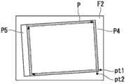
一并参照图5以及图6,液晶面板P在俯视时为长方形状,在其外周边的仅规定宽度的内侧形成具有沿着所述外周边的外部形状的显示区域P4。液晶面板P在后面叙述的第二校准装置14的面板输送上游侧以使显示区域P4的短边沿着大致输送方向的朝向被输送,在所述第二校准装置14的面板输送下游侧以使显示区域P4的长边沿着大致输送方向的朝向被输送。Referring to FIG. 5 and FIG. 6 together, liquid crystal panel P has a rectangular shape in plan view, and a display region P4 having an outer shape along the outer periphery is formed on the inner side of its outer periphery with a predetermined width. The liquid crystal panel P is conveyed on the upstream side of the panel conveyance of the second aligning
对于该液晶面板P的表面以及背面适当贴合从长条带状的第一、第二以及第三光学构件片F1、F2、F3切割出的第一、第二以及第三光学构件F11、F12、F13。在本实施方式中,作为偏振膜的第一光学构件F11以及第三光学构件F13被分别贴合在液晶面板P的背光侧以及显示面侧的两面上。作为增亮膜的第二光学构件F12与第一光学构件F11重叠地进一步被贴合在液晶面板P的背光侧的面上。The first, second, and third optical members F11, F12 cut from the strip-shaped first, second, and third optical member sheets F1, F2, and F3 are appropriately attached to the front and back of the liquid crystal panel P. , F13. In this embodiment, the 1st optical member F11 and the 3rd optical member F13 which are polarizing films are bonded to both surfaces of the backlight side of liquid crystal panel P, and the display surface side, respectively. The 2nd optical member F12 as a brightness enhancement film is further bonded on the backlight side surface of liquid crystal panel P so that the 1st optical member F11 may overlap.
如图1所示,膜贴合系统1包括:第一校准装置11,所述第一校准装置11将液晶面板P从上游工序输送至辊式输送机5的面板输送上游侧,并进行液晶面板P的校准;第一贴合装置12(一次贴合装置),所述第一贴合装置12被设置在第一校准装置11的面板输送下游侧;接近第一贴合装置12设置的第一切割装置13;以及第二校准装置14,所述第二校准装置14被设置在第一贴合装置12以及第一切割装置13的面板输送下游侧。As shown in FIG. 1 , the film laminating system 1 includes: a
又,膜贴合系统1具有:第二贴合装置15(一次贴合装置),所述第二贴合装置15被设置在第二校准装置14的面板输送下游侧;接近第二贴合装置15设置的第二切割装置16(一次切割装置);第三校准装置17,所述第三校准装置17被设置在第二贴合装置15以及第二切割装置16的面板输送下游侧;以及第三贴合装置18(二次贴合装置),所述第三贴合装置18被设置在第三校准装置17的面板输送下游侧。In addition, the film bonding system 1 has: a second bonding device 15 (primary bonding device), the
第一校准装置11保持液晶面板P并在垂直方向以及水平方向自如地输送液晶面板P,并具有一对照相机C,所述照相机C拍摄例如液晶面板P的面板输送上游侧以及下游侧的端部(参照图3)。照相机C的摄像数据被发送至控制装置20。The
控制装置20基于所述摄像数据和预先存储的后述的光轴方向的检测数据,使第一校准装置11动作。另外,后述的第二以及第三校准装置14、17也同样具有所述照相机C,该照相机C的摄像数据被用于校准。The
第一校准装置11被控制装置20控制动作,进行相对于第一贴合装置12的液晶面板P的校准。此时,液晶面板P被进行在与输送方向正交的水平方向(以下,称为零件宽度方向)上的定位,以及在绕垂直轴旋转的旋转方向(以下,仅称为旋转方向)上的定位。在该状态中,液晶面板P被导入到第一贴合装置12的贴合位置。The operation|movement of the
第一贴合装置12将输送至第一光学构件片F1上方的液晶面板P的下表面(背光侧)贴合至被导入到贴合位置的长条的第一光学构件片F1的上表面。第一贴合装置12具有:输送装置12a,所述输送装置一边从绕卷了第一光学构件片F1的第一卷材R1放卷第一光学构件片F1,一边沿着第一光学构件片F1的长度方向输送第一光学构件片F1;以及夹压辊12b,所述夹压辊12b将辊式输送机5输送的液晶面板P的下表面贴合至输送装置12a输送的第一光学构件片F1的上表面。The
输送装置12a具有:辊保持部12c,所述辊保持部12c保持绕卷了第一光学构件片F1的第一卷材R1,且沿第一光学构件片F1的长度方向不停地放出第一光学构件片F1;以及pf回收部12d,所述pf回收部12d在第一贴合装置12的面板输送下游侧回收保护膜pf,所述保护膜pf重叠在第一光学构件片F1的下表面,与第一光学构件片F1一起被不停地放出。The conveying
夹压辊12b具有轴方向相互平行地配置的一对贴合辊。在一对贴合辊之间形成所规定的间隙,该间隙内成为第一贴合装置12的贴合位置。在所述间隙内,液晶面板P以及第一光学构件片F1重叠在一起被导入。这些液晶面板P以及第一光学构件片F1一边在所述贴合辊间受夹压,一边被送出至面板输送下游侧。由此,形成第一贴合片F21,所述第一贴合片F21空出规定的间隔地在长条的第一光学构件片F1的上表面连续贴合多个液晶面板P。The nip
第一切割装置13位于pf回收部12d的面板输送下游侧。一并参照图4以及图5,第一切割装置13为了切割第一贴合片F21的第一光学构件片F1形成比显示区域P4大(在本实施方式中也比液晶面板P大)的片材F1S,横跨所述零件宽度方向的全宽切割第一光学构件片F1的所规定部位(在输送方向排列的液晶面板P之间)。另外,第一切割装置13也可以使用切割刀具,或激光切割机。通过所述切割,形成第一单面贴合面板P11,所述第一单面贴合面板P11在液晶面板P的下表面贴合有比显示区域P4大的所述片材F1S。The
参照图1,第二校准装置14保持例如辊式输送机5上的第一单面贴合面板P11,并使其围绕垂直轴90°旋转。由此,与显示区域P4的短边大致平行被输送的第一单面贴合面板P11转变方向,从而与显示区域P4的长边大致平行地被输送。另外,所述旋转是在贴合在液晶面板P的其他光学构件片的光轴方向相对于第一光学构件片F1的光轴方向呈直角配置的情况下进行。Referring to FIG. 1 , the
第二校准装置14进行与所述第一校准装置11同样的校准。即,第二校准装置14基于存储在控制装置20中的光轴方向的检测数据以及所述照相机C的摄像数据,进行第一单面贴合面板P11相对于第二贴合装置15的在零件宽度方向以及旋转方向上的定位。在该状态中,第一单面贴合面板P11被导入到第二贴合装置15的贴合位置。The
第二贴合装置15将被输送至第二光学构件片F2上方的第一单面贴合面板P11的下表面(液晶面板P的背光侧)贴合至被导入到贴合位置的长条的第二光学构件片F2的上表面。第二贴合装置15具有:输送装置15a,所述输送装置15a一边从绕卷了第二光学构件片F2的第二卷材R2放卷第二光学构件片F2,一边沿着第二光学构件片F2的长度方向输送第二光学构件片F2;以及夹压辊15b,所述夹压辊15b将辊式输送机5输送的第一单面贴合面板P11的下表面贴合至输送装置15a输送的第二光学构件片F2的上表面。The
输送装置15a具有:辊保持部15c,所述辊保持部15c保持绕卷了第二光学构件片F2的第二卷材R2,并沿第二光学构件片F2的长度方向不停放出第二光学构件片F2;以及第二回收部15d,所述第二回收部15d回收经过第二切割装置16的第二光学构件片F2的剩余部分,所述第二切割装置16位于夹压辊15b的面板输送下游侧。The conveying
夹压辊15b具有在轴方向相互平行地配置的一对贴合辊。一对贴合辊之间形成所规定的间隙,该间隙内成为第二贴合装置15的贴合位置。在所述间隙内,第一单面贴合面板P11以及第二光学构件片F2重叠在一起被导入。这些第一单面贴合面板P11以及第二光学构件片F2一边在所述贴合辊间受夹压,一边被送出至面板输送下游侧。由此,形成第二贴合片F22,所述第二贴合片F22空出规定的间隔地在长条的第二光学构件片F2的上表面连续贴合多个第一单面贴合面板P11。The nip
第二切割装置16位于夹压辊15b的面板输送下游侧。一并参照图2和图5,第二切割装置16同时切割第二光学构件片F2以及在其上表面贴合的第一单面贴合面板P11的第一光学构件片F1的片材F1S。第二切割装置16例如是CO2激光切割机,沿显示区域P4的外周缘(在本实施方式中沿着液晶面板P的外周缘)环形地切割第二光学构件片F2和第一光学构件片F1的片材F1S。通过将各光学构件片F1、F2贴合至液晶面板P后集中切割,能够提高各光学构件片F1、F2的光轴方向的精度,并消除各光学构件片F1、F2之间的光轴方向的偏差,且简化第一切割装置13的切割。The
通过第二切割装置16的切割,形成第一以及第二光学构件F11、F12被重叠贴合在液晶面板P的下表面(参照图7)的第二单面贴合面板P12。又,此时,第二单面贴合面板P12与各光学构件片F1、F2的剩余部分分离,所述各光学构件片F1、F2的剩余部分为切下与显示区域P4相对的部分(各光学构件F11、F12)后呈框状剩余的部分。第二光学构件片F2的剩余部分多个相连并形成梯子状(参照图2),该剩余部分与第一光学构件片F1的剩余部分一起被卷取至第二回收部15d。The 2nd single-sided bonding panel P12 in which 1st and 2nd optical member F11, F12 were laminated and bonded on the lower surface (refer FIG. 7) of liquid crystal panel P by the cutting of the
在此,所谓“与显示区域P4相对的部分”是表示具有显示区域P4的大小以上、液晶面板P的外部形状的大小以下的大小的区域,并且表示避开了电气零件安装部等功能部分的区域。在本实施方式中,在俯视为矩形的液晶面板P的去除了所述功能部分的三边,沿着液晶面板P的外周缘激光切割剩余部分。又,在相当于所述功能部分的一边,在从液晶面板P的外周缘适当地进入显示区域P4侧的位置激光切割剩余部分。Here, the "portion facing the display area P4" means an area having a size greater than the size of the display area P4 and less than the size of the outer shape of the liquid crystal panel P, and means avoiding functional parts such as electrical component mounting parts. area. In the present embodiment, the laser cuts the remaining part along the outer peripheral edge of the liquid crystal panel P on three sides of the liquid crystal panel P which is rectangular in plan view, except for the functional part. In addition, on the side corresponding to the functional part, the remaining part is laser-cut at a position appropriately entering the display area P4 side from the outer peripheral edge of the liquid crystal panel P. As shown in FIG.
参照图1,第三校准装置17使将液晶面板P的显示面侧作为上表面的第二单面贴合面板P12的表面和背面翻转,使液晶面板P的背光侧为上表面,且进行与所述第一以及第二校准装置11、14同样的校准。即,第三校准装置17基于存储在控制装置20中的光轴方向的检测数据以及所述照相机C的摄像数据,进行相对于第三贴合装置18的第二单面贴合面板P12在零件宽度方向以及旋转方向上的定位。在该状态下,第二单面贴合面板P12被导入到第三贴合装置18的贴合位置。1, the
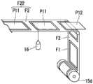
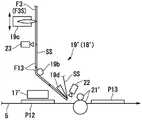
如图1以及图10所示,第三贴合装置18具有:输送装置19,所述输送装置19一边从绕卷了第三光学构件片F3和与之重叠的隔片SS的第三卷材R3放卷第三光学构件片F3以及隔片SS一边对它们进行输送,且从第三光学构件片F3切割出第三光学构件F13并将其供给至贴合位置;以及夹压辊21,所述夹压辊21将输送装置19从第三光学构件片F3切割出的第三光学构件F13的上表面贴合至辊式输送机5输送的第二单面贴合面板P12的下表面(液晶面板P的显示面侧)。As shown in FIG. 1 and FIG. 10 , the
输送装置19将隔片SS作为载体连续地输送多个第三光学构件F13。第三光学构件片F3以及隔片SS被做成长条的带状,其在所述零件宽度方向上具有与液晶面板P的显示区域P4对应的宽度(在本实施方式中,相当于显示区域P4的全宽以上且液晶面板P的全宽以下的宽度)。隔片SS与第三光学构件片F3(第三光学构件F13)重叠地能够分离地贴合在一起。以下,将隔片SS和第三光学构件片F3的组合称为第三光学构件片体F3S。The
输送装置19具有:辊保持部19a(放卷部),其对第三卷材R3进行保持,且从该第三卷材R3沿着第三光学构件片体F3S的长度方向放卷第三光学构件片体F3S;单个或多个(在图中仅示出一个)引导辊19b,其为了沿着规定的片材输送路径将从第三卷材R3放卷的第三光学构件片体F3S引导至第三贴合装置18的贴合位置而绕卷第三光学构件片体F3S的隔片SS侧;切割装置19c(切割部),其对片材输送路径上的第三光学构件片体F3S实施残留了隔片SS的半切割;刀口19d,其将实施了半切割的第三光学构件片体F3S的隔片SS侧卷挂成锐角,一边使第三光学构件F13从隔片SS分离,一边将第三光学构件F13供给至贴合位置;以及隔片回收部19e,其卷取经过刀口19d而变成单独的隔片SS。The
位于输送装置19的起点的辊保持部19a和位于输送装置19的终点的隔片回收部19e例如相互同步地驱动。由此,在辊保持部19a向第三光学构件片体F3S的输送方向放卷第三光学构件片体F3S的同时,隔片回收部19e卷取经由刀口19d而成为单独的隔片SS。The
在第三光学构件片体F3S被放卷规定长度之时,切割装置19c跨越与第三光学构件片体F3S的长度方向(放卷方向)正交的宽度方向的全宽残留隔片SS地对第三光学构件片体F3S进行切割(即仅切断第三光学构件片F3)。切割装置19c调整切割刀具的进退位置,以使得隔片SS不会由于在第三光学构件片体F3S的输送中作用的张力而破裂。When the third optical member sheet F3S is unwound to a predetermined length, the
在所述切割后的第三光学构件片体F3S上,形成有跨越第三光学构件片体F3S的宽度方向的全宽的切割线。On the 3rd optical member sheet|seat F3S after the said cut|disconnection, the cutting line which spans the full width of the width direction of the 3rd optical member sheet|seat F3S is formed.
在此,在刀口19d的顶端部附近、即第三贴合装置18的贴合位置附近的面板输送上游侧的部位,设置有对该部位的第三光学构件F13的放卷方向下游侧的切割端进行检测的第一检测照相机22。第一检测照相机22的检测信息被发送给控制装置20。控制装置20例如在第一检测照相机22检测到第三光学构件F13的下游侧端的时刻使输送装置19暂时停止。其后,在第一检测照相机22检测到第二单面贴合面板P12的下游侧端的时刻,控制装置20使输送装置19驱动,使第二单面贴合面板P12和第三光学构件F13同步并能够将它们导入至第三贴合装置18的贴合位置。Here, near the front end of the
另一方面,在第一检测照相机22的放卷方向上游侧、即相比切割装置19c位于一个第三光学构件F13程度的所述放卷方向下游侧的部位,同样设置有对第三光学构件F13的放卷方向下游侧的切割端进行检测的第二检测照相机23(检测部)。第二检测照相机23的检测信息也被发送给控制装置20。控制装置20例如在通过切割装置19c进行了第三光学构件片F3的切割后将其放卷,在第二检测照相机23检测到该切割端(第三光学构件片F3的最上游侧的切割线)的时刻,使输送装置19暂时停止。此时,采用切割装置19c进行第三光学构件片F3的切割。即、沿着第二检测照相机23的检测位置(相当于第三光学构件片F3上的第二检测照相机23的光轴延长位置)与切割装置19c的切割位置(相当于第三光学构件片F3上的切割装置19c的切割刀具进退位置)之间的片材输送路径的距离相当于第三光学构件F13的长度。On the other hand, on the upstream side of the unwinding direction of the
例如在切割出贴合于同一尺寸的液晶面板P的第三光学构件F13的情况下,在第三光学构件片体F3S的长度方向上等间隔地形成所述切割线。第三光学构件片F3通过多个切割线在长度方向上被划分为多个区域,该第三光学构件片F3上的由在长度方向相邻的一对切割线夹着的区域分别被做成第三光学构件F13。第三光学构件F13的长度在本实施方式中被设定为在显示区域P4的全长以上且在液晶面板P的全长以下。For example, when cutting out the 3rd optical member F13 bonded to the liquid crystal panel P of the same size, the said cutting line is formed at equal intervals in the longitudinal direction of the 3rd optical member sheet|seat F3S. The third optical member sheet F3 is divided into a plurality of regions in the longitudinal direction by a plurality of cutting lines, and the regions sandwiched by a pair of cutting lines adjacent in the longitudinal direction on the third optical member sheet F3 are respectively made into The third optical member F13. The length of the 3rd optical member F13 is set so that it may be more than the full length of the display area P4 and below the full length of liquid crystal panel P in this embodiment.
又,切割装置19c被设定为能够沿着第三光学构件片体F3S的片材输送路径移动。通过该移动,沿着第二检测照相机23的检测位置与切割装置19c的切割位置之间的片材输送路径的距离发生变动。切割装置19c的移动通过控制装置20控制,例如在采用切割装置19c进行第三光学构件片F3的切割之后将第三光学构件片F3放卷了一个第三光学构件F13程度的距离时,其切割端偏离规定位置的情况下,通过切割装置19c的移动来修正该偏差。Moreover, the
另外,也能够通过切割装置19c的移动来对应长度不同的第三光学构件F13的切割。又,也可以做成通过使切割装置19c以及第二检测照相机23的至少一方在片材输送方向移动,来进行所述修正或第三光学构件F13的长度变更的结构。又,切割装置19c和第二检测照相机23相互接近,但为了防止伴随着切割装置19c的移动等的第二检测照相机23的振动,切割装置19c和第二检测照相机23分别由另外的框架来支承比较理想。Moreover, the cutting of the 3rd optical member F13 from which length differs can also be corresponded by the movement of the
刀口19d被配置在辊式输送机5的下方,并在第三光学构件片体F3S的宽度方向上至少沿着第三光学构件片体F3S的全宽延伸。刀口19d将第三光学构件片体F3S卷挂成锐角,以便与半切割后的第三光学构件片体F3S的隔片SS侧滑动接触。The
第三光学构件片体F3S在刀口19d呈锐角折回之时,使第三光学构件F13从隔片SS分离。刀口19d与夹压辊21的面板输送下游侧相接近地被配置。通过刀口19d从隔片SS分离的第三光学构件F13一边与辊式输送机5所输送的液晶面板P的下表面重叠,一边被导入夹压辊21的一对贴合辊之间。The 3rd optical member sheet|seat F3S separates the 3rd optical member F13 from the spacer SS when 19 d of knife edges fold back at an acute angle. The
夹压辊21具有轴方向相互平行地被配置的一对贴合辊。The
在一对贴合辊之间形成有规定的间隙,该间隙内成为第三贴合装置18的贴合位置。在所述间隙内,第二单面贴合面板P12以及第三光学构件F13重叠在一起被导入。这些第二单面贴合面板P12以及第三光学构件F13一边在所述贴合辊间受夹压,一边被送出至面板输送下游侧。由此,形成在第二单面贴合面板P12上贴合有第三光学构件F13的两面贴合面板P13(参照图7)。A predetermined gap is formed between a pair of bonding rollers, and the inside of this gap becomes the bonding position of the
两面贴合面板P13经由未图示的缺陷检测装置被检测有无缺陷(贴合不良等)后,被输送至下游工序进行其他的处理。The double-sided bonded panel P13 is conveyed to a downstream process after having detected the presence or absence of a defect (bonding failure etc.) via the defect detection apparatus which is not shown in figure, and performs other processing.
在此,一般地,长条的光学膜(相当于各光学构件片F1、F2、F3)使得用二色性色素染色了的树脂膜单轴拉伸来制造,光学膜的光轴方向与树脂膜的延伸方向大致一致。但是,光学膜的光轴在光学膜整体中并不均一,在光学膜的宽度方向有稍许参差不齐。Here, in general, elongated optical films (corresponding to the respective optical member sheets F1, F2, and F3) are manufactured by uniaxially stretching a resin film dyed with a dichroic dye, and the optical axis direction of the optical film is aligned with the resin film. The extension direction of the film is approximately the same. However, the optical axis of the optical film is not uniform throughout the entire optical film, and is slightly uneven in the width direction of the optical film.
因此,在光学膜的宽度方向上贴合多个光学显示零件的情况下,按照光学膜的光轴方向进行光学显示零件的校准是理想的。Therefore, when bonding a plurality of optical display components in the width direction of the optical film, it is desirable to align the optical display components in accordance with the optical axis direction of the optical film.
这对抑制光学显示设备单位的光轴的参差不齐以及提高精彩度和对比度十分有效。This is very effective for suppressing the unevenness of the optical axis of the unit of the optical display device and improving the brilliance and contrast.
为了阻断除单一方向振动的光以外的光,例如,通过碘、二色性染料等将作为偏振膜的光学膜染色。另外,也可以在光学膜上进一步层压脱模膜或保护膜。In order to block light other than light vibrating in one direction, for example, an optical film as a polarizing film is dyed by iodine, a dichroic dye, or the like. In addition, a release film or a protective film may be further laminated on the optical film.
检测光学膜的光轴方向的检测装置具有:被配置在靠近光学膜的表面以及背面中的一个面的位置的光源;以及检偏振器,所述检偏振器被配置在靠近光学膜的表面以及背面中的另一个面的位置,并被配置在光源的相反侧。检偏振器通过接收从光源照射并透过光学膜的光,检测该光的强度,从而检测光学膜的光轴。检偏振器能够在例如光学膜的宽度方向移动,能够在光学膜的宽度方向的任意地方(根据使用条件选择的地方)检测光轴。The detection device that detects the optical axis direction of the optical film has: a light source that is arranged at a position close to one of the surface and the back surface of the optical film; The position of the other face in the back, and is arranged on the opposite side of the light source. The analyzer detects the optical axis of the optical film by receiving light irradiated from the light source and passing through the optical film, and detecting the intensity of the light. The analyzer can move, for example, in the width direction of the optical film, and can detect the optical axis at any position (place selected according to usage conditions) in the width direction of the optical film.
在本实施方式的情况下,由所述检测装置得到的各光学构件片F1、F2、F3的光轴方向的检测数据与各光学构件片F1、F2、F3的长度方向位置和宽度方向位置相关联地被存储在控制装置20的存储器中。该检测后,卷取各光学构件片F1、F2、F3,分别形成各卷材R1、R2、R3。以下,各光学构件片F1、F2、F3被总称为光学构件片FX、被贴合在各光学构件片F1、F2、F3的液晶面板P以及各单面贴合面板P11、P12被总称为光学显示零件PX。In the case of this embodiment, the detection data of the optical axis direction of each optical member sheet F1, F2, F3 obtained by the detection device is related to the longitudinal direction position and the width direction position of each optical member sheet F1, F2, F3 are stored in the memory of the
在此,构成光学构件片FX的偏振器件膜是单轴拉伸被例如二色性色素染色了的PVA膜而形成的,但由于拉伸时的PVA膜的厚度的不均匀或二色性色素的染色不均匀等,具有在光学构件片FX的宽度方向内侧和宽度方向外侧产生不同光轴方向的倾向。Here, the polarizer film constituting the optical member sheet FX is formed by uniaxially stretching a PVA film dyed, for example, with a dichroic dye. There exists a tendency for the optical axis direction to differ in the width direction inner side and the width direction outer side of the optical member sheet|seat FX, such as dyeing|staining nonuniformity.
因此,在本实施方式中,基于在控制装置20预先存储的光学构件片FX的各部分的光轴的面内分布的检测数据,进行贴合于此的光学显示零件PX的校准,并将光学显示零件PX贴合在光学构件片FX上。Therefore, in the present embodiment, based on the detection data of the in-plane distribution of the optical axis of each part of the optical member sheet FX stored in advance in the
具体来说,在光学构件片FX中的贴合光学显示零件PX的部位的面内,例如找出相对于规定的基准轴(长度方向轴等)的角度最大的光轴和最小的光轴,将使这些各光轴所形成的角二等分的轴作为该部位的平均光轴,以该轴为基准进行光学显示零件PX的校准。Specifically, in the surface of the portion of the optical member sheet FX where the optical display component PX is bonded, for example, the optical axis with the largest angle and the smallest optical axis with respect to a predetermined reference axis (longitudinal axis, etc.) are found, The axis that bisects the angle formed by these respective optical axes is taken as the average optical axis of the site, and the alignment of the optical display part PX is performed with reference to this axis.
由此,即使在光学构件片FX的宽度方向的不同的位置上贴合光学显示零件PX的情况下,也能抑制光学构件片FX的光轴方向相对于光学显示零件PX的基准位置的参差不齐,能够使光轴公差大致为0°(允许公差是±0.25°)。Thereby, even when the optical display components PX are bonded at different positions in the width direction of the optical member sheet FX, the deviation of the optical axis direction of the optical member sheet FX with respect to the reference position of the optical display components PX can be suppressed. Alignment, the optical axis tolerance can be approximately 0° (allowable tolerance is ±0.25°).
另外,也可以边放卷光学构件片FX,边检测光轴方向,基于该检测数据进行光学显示零件PX的校准。又,上述种种的校准方法并不限定光学构件片FX的光轴方向是0°以及90°的情况,也可适用于光轴方向被设定为任意角度(根据光学显示零件的目的的角度)的情况。In addition, the optical axis direction may be detected while unwinding the optical member sheet FX, and alignment of the optical display components PX may be performed based on the detection data. In addition, the above-mentioned various alignment methods are not limited to the case where the optical axis direction of the optical member sheet FX is 0° and 90°, but can also be applied when the optical axis direction is set to an arbitrary angle (angle according to the purpose of the optical display component) Case.
又,图3示出在具有较广宽度的光学构件片FX的宽度方向上并排贴合三个光学显示零件PX的实例。本发明并不限定于图3示出的实例,也可以采用在光学构件片FX的宽度方向上并排贴合两个以下或四个以上的光学显示零件PX的结构,也可以采用在宽度方向排列多个宽度较窄的光学构件片FX,并在这些光学构件片FX上分别贴合光学表示零件PX的结构。Moreover, the example which bonded three optical display components PX side by side in the width direction of the optical member sheet|seat FX which has a wide width is shown in FIG. The present invention is not limited to the example shown in Fig. 3, also can adopt the structure that two or less or more than four optical display parts PX are bonded side by side on the width direction of optical member sheet FX, also can adopt to arrange in the width direction A plurality of narrow optical member sheets FX are bonded to each of these optical member sheets FX with the structure of optical display parts PX.
参照图4,液晶面板P具有:由例如TFT基板构成的长方形的第一基板P1;与第一基板P1相对配置的同样为长方形的第二基板P2;以及被封入第一基板P1和第二基板P2之间的液晶层P3。另外,在图示的情况中,有时省略剖面图的各层的剖面线。Referring to FIG. 4 , the liquid crystal panel P has: a rectangular first substrate P1 made of, for example, a TFT substrate; a rectangular second substrate P2 opposite to the first substrate P1; Liquid crystal layer P3 between P2. In addition, in the case of illustration, the hatching of each layer in a cross-sectional view may be omitted.
参照图6,使得第一基板P1的外周缘的三边沿着第二基板P2的相对应的三边,且使外周缘剩余的一边向第二基板P2的相对应的一边的外侧延伸。由此,在第一基板P1的所述一边侧设置有向第二基板P2的外侧延伸的电器零件安装部P5。Referring to FIG. 6 , three sides of the outer peripheral edge of the first substrate P1 are along corresponding three sides of the second substrate P2 , and the remaining side of the outer peripheral edge extends outside the corresponding side of the second substrate P2 . Thereby, the electrical component mounting part P5 extended to the outer side of the 2nd board|substrate P2 is provided in the said one side of the 1st board|substrate P1.
参照图5,第二切割装置16边用照相机16a等检测部检测显示区域P4的外周缘,边沿显示区域P4的外周缘等切割第一以及第二光学构件片F1、F2。在显示区域P4的外侧设置规定宽度的框缘部G,在该框缘部G的宽度内利用各切割装置16、19进行激光切割,所述框缘部G配置接合第一以及第二基板P1、P2的密封剂等。Referring to FIG. 5 , the
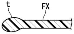
如图9所示,若单独激光切割树脂制的光学构件片FX,光学构件片FX的切割端t由于热变形产生膨胀或起伏。因此,在将激光切割后的光学构件片FX贴合至光学显示零件PX的情况下,光学构件片FX易产生混入空气或变形等贴合不良。As shown in FIG. 9, when the optical member sheet|seat FX made of resin is individually laser-cut, the cutting edge t of the optical member sheet|seat FX expands or undulates by thermal deformation. Therefore, when the optical member sheet|seat FX after laser cutting is bonded to the optical display component PX, bonding failures, such as air mixing and deformation|transformation, are easy to generate|occur|produce in optical member sheet|seat FX.
另一方面,如图8所示,在将光学构件片FX贴合在液晶面板P之后激光切割光学构件片FX的本实施方式中,光学构件片FX的切割端t被支承在液晶面板P的玻璃面。因此,由于不产生光学构件片FX的切割端t的膨胀或起伏等,且在向液晶面板P贴合光学构件片FX之后,因此不会产生所述的贴合不良。On the other hand, as shown in FIG. 8 , in this embodiment in which the optical member sheet FX is laser cut after the optical member sheet FX is bonded to the liquid crystal panel P, the cut end t of the optical member sheet FX is supported on the edge of the liquid crystal panel P. glass surface. Therefore, after bonding optical member sheet|seat FX to liquid crystal panel P, since expansion, undulation, etc. of the cut edge t of optical member sheet|seat FX do not generate|occur|produce, the said bonding defect does not generate|occur|produce.
在液晶面板P上切割光学构件片FX这样的情况下,激光加工机的切割线的偏差宽度(公差)比切割刀具的切割线的偏差宽度小。因此在本实施方式中,与使用切割刀具切割光学构件片FX的情况相比,能够缩小所述框缘部G的宽度,能够使液晶面板P小型化以及(或者)显示区域P4大型化。这样的光学构件片对如近年的智能手机或触屏终端那样的、限制壳体的尺寸且要求扩大显示画面的高性能移动信息终端的适用也是有效的。When cutting the optical member sheet|seat FX on liquid crystal panel P, the variation width (tolerance) of the cutting line of a laser processing machine is smaller than the variation width of the cutting line of a cutting blade. Therefore, in this embodiment, compared with the case where the optical member sheet|seat FX is cut|disconnected using a dicing blade, the width|variety of the said frame edge part G can be narrowed, and liquid crystal panel P can be miniaturized and (or) display area P4 can be enlarged. Such an optical member sheet is also effective for application to high-performance mobile information terminals that limit the size of a housing and require an enlarged display screen, such as recent smartphones or touch-panel terminals.
在此,由于在将光学构件片FX切割为整合到液晶面板P的显示区域P4的片材后输送到别的生产线并贴合在液晶面板P的情况下,所述片材以及液晶面板P各自的尺寸公差及这些相对贴合位置的尺寸公差重叠,因此缩小液晶面板P的框缘部G的宽度变得困难(扩大显示区域变得困难)。Here, when the optical member sheet FX is cut into a sheet integrated into the display area P4 of the liquid crystal panel P and then transported to another production line and bonded to the liquid crystal panel P, the sheet and the liquid crystal panel P each The dimensional tolerances and the dimensional tolerances of these relative bonding positions overlap, so it becomes difficult to narrow the width of the frame portion G of the liquid crystal panel P (it becomes difficult to expand the display area).
另一方面,在将光学构件片FX贴合在液晶面板后,按照显示区域P4切割光学构件片FX的情况下,只考虑切割线的偏差公差就能够缩小框缘部G的宽度公差(±0.1mm以下)。该点也可缩小液晶面板P的框缘部G的宽度(扩大显示区域成为可能)。On the other hand, after bonding the optical member sheet FX to the liquid crystal panel, when the optical member sheet FX is cut according to the display area P4, the width tolerance of the frame edge part G can be narrowed (±0.1 mm or less). This point also makes it possible to reduce the width of the frame portion G of the liquid crystal panel P (it becomes possible to expand the display area).
进一步,通过不用刀具而是用激光切割液晶面板P上的光学构件片FX,切割时的力度不输入至液晶面板P,在液晶面板P的基板的端缘很难产生裂缝或缺陷,提高对于热循环等的耐久性。同样的,由于不接触液晶面板P,对于电气零件安装部P5的损害也少。Furthermore, by cutting the optical member sheet FX on the liquid crystal panel P with a laser instead of a cutter, the strength during cutting is not input to the liquid crystal panel P, and it is difficult to generate cracks or defects at the edge of the substrate of the liquid crystal panel P, thereby improving thermal resistance. Durability of cycles etc. Similarly, since it does not touch liquid crystal panel P, there is little damage to electrical component mounting part P5.
又,第三贴合装置18将具有与显示区域P4对应的宽度的带状的第三光学构件片F3切割成规定长度而形成第三光学构件F13。第三贴合装置18一边与隔片SS一起输送该第三光学构件F13,一边在进行所述切割的生产线内将它们贴合于第二单面贴合面板P12。因此,与将按照显示区域P4加工了的偏光板输送至别的生产线这样的情况相比,第三光学构件F13的尺寸参差不齐或贴合参差不齐的影响得以抑制。Moreover, the
如图6所示,在用激光切割光学构件片FX(图6中的第二光学构件片F2)的情况下,例如将激光切割的起点pt1设定在显示区域P4的一个长边的延长线上,从该起点pt1首先开始切割所述一个长边。激光切割的终点pt2设定在激光绕显示区域P4一圈到达显示区域P4的起点侧的短边的延长线上的位置。起点pt1以及终点pt2被设定为在光学构件片FX的剩余部分留下规定的连接部分,从而能耐受卷取光学构件片FX时的张力。As shown in FIG. 6, in the case of cutting the optical member sheet FX (the second optical member sheet F2 in FIG. 6 ) with a laser, for example, the starting point pt1 of laser cutting is set on the extended line of one long side of the display area P4. , start cutting the one long side first from the starting point pt1. The end point pt2 of laser cutting is set at the position on the extension line of the short side on the starting point side where the laser light goes around the display area P4 and reaches the display area P4. The starting point pt1 and the end point pt2 are set so that a predetermined connection portion can be left in the remainder of the optical member sheet FX, and the tension at the time of winding up the optical member sheet FX can be tolerated.
如以上说明的那样,上述实施方式的光学显示设备的生产系统为,在构成将光学构件F11、F12、F13贴合在液晶面板P上而形成的光学显示设备的生产系统的一部分的膜贴合系统1中,包括:贴合装置12、15,所述贴合装置12、15对于在辊式输送机5上输送的多个光学显示零件PX,边从卷材R1、R2放卷带状的光学构件片F1、F2,边依次将第二光学构件片F2以及多个液晶面板P的第一面(表面以及背面中的一个面)贴合在第一光学构件片F1做成第二贴合片F22,所述光学构件片F1、F2在与光学显示零件PX的输送方向正交的零件宽度方向具有比液晶面板P的显示区域的宽度大的宽度;以及第二切割装置16,所述第二切割装置16通过将与所述显示区域P4相对的所述光学构件片F1、F2的相对部分和位于所述相对部分的外侧的剩余部分切割开,并从所述光学构件片F1、F2切割出具有与所述显示区域P4对应大小的光学构件F11、F12,从而从所述第二贴合片F22切割出第二单面贴合面板P12,所述第二单面贴合面板P12包括单一的所述液晶面板P以及与所述液晶面板P重叠的所述光学构件F11、F12;以及第三切割装置18,所述第三切割装置18对于在辊式输送机5上输送的多个所述第二单面贴合面板P12,将在所述零件宽度方向上具有与所述显示区域P4对应的宽度的带状的第三光学构件片F3和隔片SS一起从第三卷材R3放卷,每次以与所述显示区域P4对应的长度放卷第三光学构件片F3就在该第三光学构件片F3上实施沿着宽度方向的切割,做成具有与所述显示区域P4对应的大小的第三光学构件F13之后,将所述隔片SS作为载体输送多个所述第三光学构件F13,同时将所述第三光学构件F13贴合于所述第二单面贴合面板P12上的所述液晶面板P的第二面(与第一面相反的面、表面以及背面中的另一面)上。As described above, the production system of the optical display device according to the above-mentioned embodiment is film bonding to a part of the production system of the optical display device formed by bonding the optical members F11, F12, and F13 to the liquid crystal panel P. In the system 1, it includes: laminating
根据该结构,将具有与显示区域P4对应的宽度的带状的第三光学构件片F3切割成规定长度而形成第三光学构件F13,一边将与第三光学构件片F3一起放卷的隔片SS做为载体输送该第三光学构件F13,一边在进行所述切割的生产线内在液晶面板P贴合第三光学构件F13。因此,与将按照显示区域P4加工了的偏光板输送至别的生产线这样的情况相比,能够抑制第三光学构件F13的尺寸参差不齐或贴合参差不齐,缩小显示区域P4周边的框缘部G,谋求显示区域的扩大以及设备的小型化。According to this configuration, the strip-shaped third optical member sheet F3 having a width corresponding to the display area P4 is cut into a predetermined length to form the third optical member F13, and the spacer that is unwound with the third optical member sheet F3 SS transports this 3rd optical member F13 as a carrier, and bonds 3rd optical member F13 to liquid crystal panel P in the production line which performs said cutting. Therefore, compared with the case where the polarizing plate processed according to the display area P4 is transported to another production line, it is possible to suppress the size variation or bonding unevenness of the third optical member F13, and reduce the size of the frame around the display area P4. The edge G seeks to expand the display area and reduce the size of the device.
又,通过将贴合至液晶面板P后的光学构件片F1、F2的切割与残留隔片SS的半切割后的第三光学构件片F3的贴合相组合,能够谋求框缘部G的缩小和生产节拍时间的缩短。Furthermore, by combining the cutting of the optical member sheets F1 and F2 bonded to the liquid crystal panel P and the bonding of the third optical member sheet F3 after the half-cut with the spacer SS left, the size of the frame edge G can be achieved. and reduction in takt time.
又,上述光学显示设备的生产系统的所述第三贴合装置18具有:辊保持部19a,其将所述第三光学构件片F3和所述隔片SS一起放卷;切割装置19c,其对所述第三光学构件片F3实施切割并做成所述第三光学构件F13;第二检测照相机23,其在与对所述第三光学构件片F3实施切割的切割位置相比,在所述第三光学构件片F3的放卷方向上向下游侧隔开与一个所述第三光学构件F13对应的距离的位置,对通过所述切割形成在所述第三光学构件片F3上的切割线进行检测;以及控制装置20,在从所述切割位置向下游侧隔开一个所述第三光学构件F13的距离的检测位置检测到所述切割线时,控制装置20根据所述切割线的位置对所述切割位置和所述检测位置之间的距离进行调整。In addition, the
根据该结构,在通过相比第三光学构件片F3的切割位置位于一个第三光学构件F13程度的下游侧的第二检测照相机23检测到所述第三光学构件F13的放卷方向下游侧端时,通过切割装置19c对第三光学构件片F3实施切割成为可能,可以得到规定长度的第三光学构件F13。又,即使第三光学构件片F3的放卷量产生误差,通过基于第二检测照相机23的检测信息的切割装置19c的相对移动也能够对所述误差进行修正(吸收)。因此,可以确保第三光学构件F13的长度的精度,且也可以与长度不同的第三光学构件F13的切割相对应。According to this configuration, the downstream end of the third optical member F13 in the unwinding direction is detected by the
在此,上述实施方式中的光学显示设备的生产方法为,对于在辊式输送机5上输送的多个光学显示零件PX,边从卷材R1、R2放卷在与光学显示零件PX的输送方向正交的零件宽度方向上具有比液晶面板P的显示区域P4的宽度大的宽度的带状的光学构件片F1、F2,边依次将第二光学构件片F2以及多个液晶面板P的第一面贴合在第一光学构件片F1上做成第二贴合片F22,通过将与所述显示区域P4相对的所述光学构件片F1、F2的相对部分和位于所述相对部分的外侧的剩余部分切割开,并从所述光学构件片F1、F2切割出具有与所述显示区域P4对应大小的光学构件F11、F12,从而从所述第二贴合片F22切割出第二单面贴合面板P12,所述第二单面贴合面板P12包括单一的所述液晶面板P以及与所述液晶面板P重叠的所述光学构件F11、F12,对于在辊式输送机5上输送的多个所述第二单面贴合面板P12,将在所述零件宽度方向上具有与所述显示区域P4对应的宽度的带状的第三光学构件片F3和隔片SS一起从第三卷材R3放卷,每次以与所述显示区域P4对应的长度放卷第三光学构件片F3就在该第三光学构件片F3上实施沿着宽度方向的切割,做成具有与所述显示区域P4对应的大小的第三光学构件F13之后,一边将所述隔片SS作为载体输送多个所述第三光学构件F13,一边将所述第三光学构件F13贴合于所述第二单面贴合面板P12上的所述液晶面板P的第二面上。Here, in the production method of the optical display device in the above-described embodiment, for the plurality of optical display parts PX conveyed on the
另外,图11示出膜贴合系统1的变形例。其相对于图1的结构,在具有代替所述第一贴合装置12的第一贴合装置12’,以及代替所述第一切割装置13的第一切割装置13’这一点上尤其不同。对变形例中的其他结构与所述实施方式相同的结构,赋予相同符号,省略详细说明。In addition, FIG. 11 has shown the modification of the film bonding system 1. As shown in FIG. Compared with the structure of FIG. 1 , it is particularly different in that it has a first bonding device 12' instead of the
第一贴合装置12’具有代替所述输送装置12a的输送装置12a’。输送装置12a’与所述输送装置12a相比,除具有辊保持部12c以及pf回收部12d外,进一步具有第一回收部12e,所述第一回收部12e卷取经过第一切割装置13’被切剩为梯子状的第一光学构件片F1的剩余部分。The first bonding device 12' has a conveying
第一切割装置13’位于pf回收部12d的面板输送下游侧,第一回收部12e的面板输送上游侧,为了从第一光学构件片F1切下比显示区域P4大的片材,而切割第一光学构件片F1。第一切割装置13’是与所述第二切割装置16相同的激光加工机,沿显示区域P4外侧的规定路线环形地切割第一光学构件片F1。The first cutting device 13' is located on the downstream side of the panel conveyance of the
通过第一切割装置13’的切割,形成在液晶面板P的下表面贴合有比显示区域P4大的第一光学构件片F1的片材的第一单面贴合面板P11’。又,此时,第一单面贴合面板P11’和被切剩为梯子状的第一光学构件片F1的剩余部分被分离,第一光学构件片F1的剩余部分被第一回收部12e卷取。The first single-sided bonding panel P11' in which the sheet of the first optical member sheet F1 larger than the display area P4 is bonded to the lower surface of the liquid crystal panel P is formed by cutting by the first cutting device 13'. Also, at this time, the first single-sided laminated panel P11' is separated from the remaining portion of the first optical member sheet F1 cut into a ladder shape, and the remaining portion of the first optical member sheet F1 is wound up by the
又,图12示出膜贴合系统1的其他的变形例。其对于图1的结构,在具有代替所述第三校准装置17以及第三贴合装置18的第三校准装置17’以及第三贴合装置18’这一点上尤其不同。对变形例中的其他结构与所述实施方式相同的结构,赋予相同符号,省略详细说明。Moreover, another modification of the film bonding system 1 is shown in FIG. 12. It is particularly different from the structure of FIG. 1 in that it has a
第三校准装置17’相比于所述第三校准装置17,没有使面板表面和背面翻转的功能,只具有与所述第一以及第二校准装置11、14相同的校准功能,是比较简单的结构。即,第三校准装置17’,基于存储在控制装置20中的光轴方向的检查数据以及所述照相机C的摄像数据,进行第二单面贴合面板P12相对于第三贴合装置18的在零件宽度方向以及旋转方向上的定位。在该状态下,第二单面贴合面板P12被导入到第三贴合装置18’的贴合位置。Compared with the
第三贴合装置18’与所述第三贴合装置18相比,将输送至第三光学构件片F3下方的第二单面贴合面板P12的上表面(液晶面板P的显示面侧)贴合至被导入到贴合位置的长条的第三光学构件片F3的下表面。第三贴合装置18’具有输送装置19’以及夹压辊21’,该输送装置19’以及夹压辊21’具有使设置有所述输送装置19以及夹压辊21的位置颠倒的结构。由此,第三光学构件片F3的贴合面向下,可抑制对于该贴合面的划伤或尘土等的异物的附着。The
另外,本发明不限于上述实施方式以及变形例,例如与所述第三贴合装置18’相同,使设置有第一以及第二贴合装置12、15的位置颠倒也成为可能。又,像这样使设置位置颠倒的各贴合装置和所述第一贴合装置12’以及第一切割装置13’进行适当组合也成为可能。进一步地,将第一以及第二贴合装置12、15做成与第三贴合装置18相同的结构也成为可能。这种结构将在以下第二实施方式中进行叙述。In addition, the present invention is not limited to the above-mentioned embodiments and modifications, and for example, it is possible to reverse the positions where the first and
(第二实施方式)(second embodiment)
以下,参照附图对本发明的第二实施方式进行说明。在本实施方式中,作为光学显示设备的生产系统,对构成其一部分的膜贴合系统进行说明。Hereinafter, a second embodiment of the present invention will be described with reference to the drawings. In this embodiment, as a production system of an optical display device, a film bonding system constituting a part thereof will be described.
在第二实施方式中,对与第一实施方式相同的构件赋予相同符号,省略或简化其说明。In the second embodiment, the same symbols are assigned to the same components as those in the first embodiment, and descriptions thereof are omitted or simplified.
特别是,如以下具体叙述的那样,在第一实施方式的膜贴合系统中,贴合装置112、115、118被配置在辊式输送机105之上,切割装置113被配置在辊式输送机105之下。In particular, as described in detail below, in the film bonding system of the first embodiment, the
图13是示出本实施方式的膜贴合系统101的概略结构。膜贴合系统101例如在液晶面板或有机EL面板等面板状的光学显示零件上,贴合偏振膜或相位差膜、增亮膜等膜状的光学构件。膜贴合系统101制造包含所述光学显示零件以及光学构件的光学构件贴合体。在膜贴合系统101中,使用液晶面板P作为所述光学显示零件。膜贴合系统101的各个部分由作为电子控制装置的控制装置120(控制部)总括控制。FIG. 13 shows a schematic configuration of the
膜贴合系统101是一边使用例如驱动式的辊式输送机105(生产线)从贴合工序的始发位置到终点位置输送液晶面板P,一边对液晶面板P依次施行处理。以使液晶面板P的表面以及背面为水平的状态在辊式输送机5上输送液晶面板P。The
另外,图中左侧示出液晶面板P的输送方向上游侧(以下,称为面板输送上游侧),图中右侧示出液晶面板P的输送方向下游侧(以下,称为面板输送下游侧)。In addition, the left side of the figure shows the upstream side of the transport direction of the liquid crystal panel P (hereinafter referred to as the upstream side of panel transport), and the right side of the figure shows the downstream side of the transport direction of the liquid crystal panel P (hereinafter referred to as the downstream side of panel transport). ).
在第二实施方式中使用的液晶面板与上述第一实施方式的液晶面板P相同(参照图5以及图6)。The liquid crystal panel used in the second embodiment is the same as the liquid crystal panel P in the first embodiment described above (see FIGS. 5 and 6 ).
液晶面板P在后面叙述的第二校准装置114的面板输送上游侧以使显示区域P4的短边沿着大致输送方向的朝向被输送,在所述第二校准装置114的面板输送下游侧以使显示区域P4的长边沿着大致输送方向的朝向被输送。The liquid crystal panel P is conveyed on the upstream side of the panel conveyance of the
如图13所示,膜贴合系统101包括:第一校准装置111,所述第一校准装置111将液晶面板P从上游工序输送至辊式输送机105的面板输送上游侧上,并进行液晶面板P的校准;第一贴合装置112(一次贴合装置),所述第一贴合装置112被设置在第一校准装置111的面板输送下游侧;接近第一贴合装置112设置的第一切割装置113;以及第二校准装置114,所述第二校准装置114被设置在第一贴合装置112以及第一切割装置113的面板输送下游侧。As shown in FIG. 13 , the
又,膜贴合系统101具有:第二贴合装置115(一次贴合装置),所述第二贴合装置115被设置在第二校准装置114的面板输送下游侧;接近第二贴合装置115设置的第二切割装置116(一次切割装置);第三校准装置117,所述第三校准装置117被设置在第二贴合装置115以及第二切割装置116的面板输送下游侧;以及第三贴合装置118(二次贴合装置),所述第三贴合装置118被设置在第三校准装置117的面板输送下游侧。In addition, the
第一校准装置111保持液晶面板P并在垂直方向以及水平方向自如地输送液晶面板P,且具有一对照相机C,所述照相机C拍摄例如液晶面板P的面板输送上游侧以及下游侧的端部(参照图15)。照相机C的摄像数据被发送至控制装置120。控制装置120基于所述摄像数据和预先存储的后述的光轴方向的检测数据,使第一校准装置111动作。另外,后述的第二以及第三校准装置114、117也同样具有所述照相机C,该照相机C的摄像数据用于校准。The
第一校准装置111被控制装置120控制动作,进行相对于第一贴合装置112的液晶面板P的校准。此时,液晶面板P被进行在与输送方向正交的水平方向(以下,称为零件宽度方向)的定位,以及在绕垂直轴旋转的旋转方向(以下,仅称为旋转方向)的定位。在该状态下,液晶面板P被导入到第一贴合装置112的贴合位置。The
第一贴合装置112,将输送至第一光学构件片F1下方的液晶面板P的上表面(背光侧)贴合到被导入到贴合位置的长条的第一光学构件片F1的下表面。第一贴合装置112具有:输送装置112a,所述输送装置112a一边从绕卷了第一光学构件片F1的第一卷材R1放卷第一光学构件片F1,一边沿着第一光学构件片F1的长度方向输送第一光学构件片F1;以及夹压辊112b,所述夹压辊112b将辊式输送机105输送的液晶面板P的上表面贴合至输送装置112a输送的第一光学构件片F1的下表面。The
输送装置112a具有:辊保持部112c,所述辊保持部112c保持绕卷了第一光学构件片F1的第一卷材R1,并沿第一光学构件片F1的长度方向不停地放出第一光学构件片F1;以及pf回收部112d,所述pf回收部112d在第一贴合装置112的面板输送下游侧回收保护膜pf,所述保护膜pf重叠在第一光学构件片F1的上表面,与第一光学构件片F1一起被不停放出。输送装置112a在第一贴合装置112的贴合位置设定第一光学构件片F1的输送路径,从而使被贴合在液晶面板P的第一光学构件片F1的贴合面朝向下方。The conveying
夹压辊112b具有轴方向相互平行地配置的一对贴合辊。在一对贴合辊之间形成所规定的间隙,该间隙内成为第一贴合装置112的贴合位置。在所述间隙内,液晶面板P以及第一光学构件片F1重叠在一起被导入。这些液晶面板P以及第一光学构件片F1边在所述贴合辊间受夹压,边被送出到面板输送下游侧。由此,形成空出规定的间隔地在长条的第一光学构件片F1的下表面连续贴合多个液晶面板P的第一贴合片F21。The nip
第一切割装置113位于pf回收部112d的面板输送下游侧。一并参照图4以及图5,第一切割装置113为了切割第一贴合片F21的第一光学构件片F1形成比显示区域P4大(在本实施方式中也比液晶面板P大)的片材F1S,横跨所述零件宽度方向的整个宽度切割第一光学构件片F1的所规定部位(在输送方向排列的液晶面板P之间)。另外,第一切割装置113也可以使用切割刀具,或激光刀具。通过所述切割,形成在液晶面板P的上表面贴合有比显示区域P4大的所述片材F1S的第一单面贴合面板P11。The
参照图13,第二校准装置114保持例如辊式输送机105上的第一单面贴合面板P11,并使其围绕垂直轴90°旋转。由此,与显示区域P4的短边大致平行地被输送的第一单面贴合面板P11转变方向,从而与显示区域P4的长边大致平行地被输送。另外,所述旋转在贴合于液晶面板P的其他的光学构件片的光轴方向相对于第一光学构件片F1的光轴方向呈直角配置的情况下进行。Referring to FIG. 13 , the
第二校准装置114进行与所述第一校准装置111同样的校准。即,第二校准装置114基于存储在控制装置120中的光轴方向的检查数据以及所述照相机C的摄像数据,进行第一单面贴合面板P11相对于第二贴合装置115的在零件宽度方向以及旋转方向上的定位。在该状态下,第一单面贴合面板P11被导入到第二贴合装置115的贴合位置。The
第二贴合装置115将输送至第二光学构件片F2下方的第一单面贴合面板P11的上表面(液晶面板P的背光侧)贴合至被导入到贴合位置的长条的第二光学构件片F2的下表面。第二贴合装置115具有:输送装置115a,所述输送装置115a一边从绕卷了第二光学构件片F2的第二卷材R2放卷第二光学构件片F2,一边沿着第二光学构件片F2的长度方向输送第二光学构件片F2;以及夹压辊115b,所述夹压辊115b将辊式输送机105输送的第一单面贴合面板P11的上表面贴合至输送装置115a输送的第二光学构件片F2的下表面。The
输送装置115a具有:辊保持部115c,所述辊保持部115c保持绕卷了第二光学构件片F2的第二卷材R2,并沿第二光学构件片F2的长度方向不停地放出第二光学构件片F2;以及第二回收部115d,所述第二回收部115d回收经过第二切割装置116的第二光学构件片F2的剩余部分,所述第二切割装置116位于夹压辊115b的面板输送下游侧。输送装置115a在第二贴合装置115的贴合位置设定第二光学构件片F2的输送路径,从而使被贴合在第一单面贴合面板P11的第二光学构件片F2的贴合面朝向下方。The conveying
夹压辊115b具有轴方向相互平行地配置的一对贴合辊。在一对贴合辊之间形成所规定的间隙,该间隙内成为第二贴合装置115的贴合位置。在所述间隙内,第一单面贴合面板P11以及第二光学构件片F2重叠在一起被导入。这些第一单面贴合面板P11以及第二光学构件片F2边在所述贴合辊间受夹压,边被送出至面板输送下游侧。由此,形成空出规定的间隔地将多个第一单面贴合面板P11连续地贴合于长条的第二光学构件片F2的下表面的第二贴合片F22。The nip
第二切割装置116位于夹压辊115b的面板输送下游侧。一并参照图14和图5,第二切割装置116同时切割第二光学构件片F2以及在其下表面贴合的第一单面贴合面板P11的第一光学构件片F1的片材F1S。第二切割装置116具有与第一实施方式的第二切割装置16相同的结构。通过使用第二切割装置116,能够提高各光学构件片F1、F2的光轴方向的精度,并消除各光学构件片F1、F2之间的光轴方向的偏差,且简化第一切割装置13的切割。The
通过第二切割装置116的切割,形成在液晶面板P的上表面重叠贴合有第一以及第二光学构件F11、F12(参照图7)的第二单面贴合面板P12。又,此时,第二单面贴合面板P12与各光学构件片F1、F2的剩余部分分离,所述各光学构件片F1、F2的剩余部分是切下与显示区域P4相对的部分(各光学构件F11、F12)而剩余为框状的部分。第二光学构件片F2的剩余部分多个相连并形成为梯子状(参照图14),该剩余部分与第一光学构件片F1的剩余部分一起被卷取至第二回收部115d。The 2nd single-sided bonding panel P12 which laminated|bonded the 1st and 2nd optical member F11, F12 (refer FIG. 7) on the upper surface of liquid crystal panel P by the cutting of the
参照图13,第三校准装置117使将液晶面板P的背光侧作为上表面的第二单面贴合面板P12的表面和背面翻转,使液晶面板P的显示面侧为上表面,并进行与所述第一以及第二校准装置111、114同样的校准。即,第三校准装置117,基于存储在控制装置120中的光轴方向的检测数据以及所述照相机C的摄像数据,进行第二单面贴合面板P12相对于第三贴合装置118的在零件宽度方向上的定位以及旋转方向上的定位。在该状态下,第二单面贴合面板P12被导入到第三贴合装置118的贴合位置。Referring to FIG. 13 , the
如图13以及图16所示,第三贴合装置118具有:输送装置119,所述输送装置119一边从绕卷了第三光学构件片F3和与之重叠的隔片SS的第三卷材R3放卷第三光学构件片F3以及隔片SS一边输送,且从第三光学构件片F3切割出第三光学构件F13并将其供给至贴合位置;以及夹压辊121,所述夹压辊121将辊式输送机105输送的第二单面贴合面板P12的上表面(液晶面板P的显示面侧)贴合至输送装置119从第三光学构件片F3切割出的第三光学构件F13的下表面。As shown in FIG. 13 and FIG. 16 , the
输送装置119与第一实施方式的输送装置19同样地将隔片作为载体连续地输送多个第三光学构件F13。输送装置119具有:辊保持部119a(放卷部),其对第三卷材R3进行保持,且从该第三卷材R3沿着第三光学构件片体F3S的长度方向放卷第三光学构件片体F3S;单个或多个(在图中仅示出一个)引导辊119b,其为了沿着规定的片材输送路径将从第三卷材R3放卷的第三光学构件片体F3S引导至第三贴合装置118的贴合位置而卷挂第三光学构件片体F3S的隔片SS侧;切割装置119c(切割部),其对片材输送路径上的第三光学构件片体F3S实施残留了隔片SS的半切割;刀口119d,其将实施了半切割的第三光学构件片体F3S的隔片SS侧卷挂成锐角,一边使第三光学构件F13从隔片SS分离,一边将三光学构件F13供给至贴合位置;以及隔片回收部119e,其卷取经过刀口119d而变成单独的隔片SS。The
位于输送装置119的起点的辊保持部119a和位于输送装置119的终点的隔片回收部119e例如相互同步地驱动。由此,在辊保持部119a向第三光学构件片体F3S的输送方向放卷第三光学构件片体F3S的同时,隔片回收部119e卷取经由刀口19d而成为单独的隔片SS。The
在第三光学构件片体F3S被放卷规定长度之时,切割装置119c跨越与第三光学构件片体F3S的长度方向(放卷方向)正交的宽度方向的全宽残留隔片SS地对第三光学构件片体F3S进行切割(即仅切断第三光学构件片F3)。切割装置119c调整切割刀具的进退位置,以使得隔片SS不会由于在第三光学构件片体F3S的输送中作用的张力而破裂。When the third optical member sheet F3S is unwound to a predetermined length, the
在所述切割后的第三光学构件片体F3S上,形成有跨越第三光学构件片体F3S的宽度方向的全宽的切割线。On the 3rd optical member sheet|seat F3S after the said cut|disconnection, the cutting line which spans the full width of the width direction of the 3rd optical member sheet|seat F3S is formed.
在此,在刀口119d的顶端部附近、即第三贴合装置118的贴合位置附近的面板输送上游侧的部位,设置有对该部位的第三光学构件F13的放卷方向下游侧的切割端进行检测的第一检测照相机122。第一检测照相机122的检测信息被发送给控制装置120。控制装置120例如在第一检测照相机122检测到第三光学构件F13的下游侧端的时刻使输送装置119暂时停止。其后,在第一检测照相机122检测到第二单面贴合面板P12的下游侧端的时刻,控制装置120使输送装置119驱动,使第二单面贴合面板P12和第三光学构件F13同步并能够将它们导入至第三贴合装置118的贴合位置。Here, near the front end of the
另一方面,在第一检测照相机122的放卷方向上游侧、即相比切割装置119c位于一个第三光学构件F13程度的所述放卷方向下游侧的部位,同样设置有对第三光学构件F13的放卷方向下游侧的切割端进行检测的第二检测照相机123。第二检测照相机123的检测信息也被发送给控制装置120。控制装置120例如在通过切割装置119c进行了第三光学构件片F3的切割后将其放卷,在第二检测照相机123检测到该切割端(第三光学构件片F3的最上游侧的切割线)的时刻,使输送装置119暂时停止。此时,采用切割装置119c进行第三光学构件片F3的切割。即、沿着第二检测照相机123的检测位置(相当于第三光学构件片F3上的第二检测照相机123的光轴延长位置)与切割装置119c的切割位置(相当于第三光学构件片F3上的切割装置119c的切割刀具进退位置)之间的片材输送路径的距离相当于第三光学构件F13的长度。On the other hand, on the upstream side of the unwinding direction of the
又,切割装置119c被设定为能够沿着第三光学构件片体F3S的片材输送路径移动。通过该移动,沿着第二检测照相机123的检测位置与切割装置119c的切割位置之间的片材输送路径的距离发生变动。切割装置119c的移动通过控制装置120控制,例如在采用切割装置119c进行第三光学构件片F3的切割之后将第三光学构件片F3放卷了一个第三光学构件F13程度的距离时,其切割端偏离规定位置的情况下,通过切割装置119c的移动来修正该偏差。Moreover, the
另外,也可以通过切割装置119c的移动来对应长度不同的第三光学构件F13的切割。又,可以做成通过使切割装置119c以及第二检测照相机123的至少一方在片材输送方向移动,来进行所述修正或第三光学构件F13的长度变更的结构。又,切割装置119c和第二检测照相机123相互接近,但为了防止伴随着切割装置119c的移动等的第二检测照相机123的振动,切割装置119c和第二检测照相机123分别由另外的框架来支承比较理想。In addition, the cutting of the third optical member F13 having different lengths may be supported by the movement of the
刀口119d被配置在辊式输送机105的下方,并在第三光学构件片体F3S的宽度方向上至少沿着第三光学构件片体F3S的全宽延伸。刀口119d将第三光学构件片体F3S卷挂成锐角,以便与半切割后的第三光学构件片体F3S的隔片SS侧滑动接触。The
第三光学构件片体F3S在刀口119d呈锐角折回之时,使第三光学构件F13从隔片SS分离。刀口119d与夹压辊121的面板输送下游侧相接近地配置。通过刀口119d从隔片SS分离的第三光学构件F13一边与辊式输送机105所输送的液晶面板P的上表面重叠,一边被导入夹压辊121的一对贴合辊之间。The 3rd optical member sheet|seat F3S separates the 3rd optical member F13 from the spacer SS when 119 d of knife edges fold back at an acute angle. The
夹压辊121具有轴方向相互平行地配置的一对贴合辊。在一对贴合辊之间形成所规定的间隙,该间隙内成为第三贴合装置118的贴合位置。在所述间隙内,第二单面贴合面板P12以及第三光学构件F13重叠在一起被导入。这些第二单面贴合面板P12以及第三光学构件F13边在所述贴合辊间受夹压,边被送出至面板输送下游侧。由此,形成在第二单面贴合面板P12上贴合有第三光学构件F13的两面贴合面板P13。(参照图7)。The nip
与上述第一实施方式的切割装置19相同,两面贴合面板P13经由未图示的缺陷检测装置被检测有无缺陷(贴合不良等)后,被输送至下游工序进行其他的处理。Similar to the
又,与上述第一实施方式的控制装置20同样,在本实施方式的情况下,由所述检测装置得到的各光学构件片F1、F2、F3的光轴方向的检查数据与各光学构件片F1、F2、F3的长度方向位置和宽度方向位置相关联地被存储在控制装置120的存储器中。又,与上述第一实施方式同样,检查后卷取各光学构件片F1、F2、F3从而分别形成卷材R1、R2、R3。Also, similar to the
在本实施方式中,与第一实施方式的控制装置20相同,基于在控制装置120预先存储的光学构件片FX的各部分的光轴的面内分布的检测数据,进行贴合于此的光学显示零件PX的校准,并将光学显示零件PX贴合在光学构件片FX上。由此,得到与第一实施方式相同的效果。In this embodiment, similar to the
又,图15示出在宽度较广的光学构件片FX的宽度方向上并排贴合三个光学显示零件PX的实例,但并不限定于此,也可以是在光学构件片FX的宽度方向上并排贴合两个以下或四个以上的光学显示零件PX的结构,也可以是在宽度方向排列多个宽度较窄的光学构件片FX,并在它们各自上分别贴合光学表示零件PX的结构。Also, Fig. 15 shows an example in which three optical display components PX are bonded side by side in the width direction of the wider optical member sheet FX, but it is not limited thereto, and it may also be in the width direction of the optical member sheet FX A structure in which two or less or four or more optical display parts PX are bonded side by side, or a structure in which a plurality of narrow optical member sheets FX are arranged in the width direction, and optical display parts PX are bonded to each of them .
参照图5,第二切割装置116边用照相机116a等检测部检测显示区域P4的外周缘,边沿显示区域P4的外周缘等切割第一以及第二光学构件片F1、F2。在显示区域P4的外侧设置有规定宽度的框缘部G,在该框缘部G的宽度内利用第二切割装置116进行激光切割,所述框缘部G配置接合第一以及第二基板P1、P2的密封剂等。Referring to FIG. 5 , the
通过使用这样的切割装置,能得到与第一实施方式同样的效果(参照图9以及图10)。By using such a cutting device, the same effect as that of the first embodiment can be obtained (see FIGS. 9 and 10 ).
又,第三贴合装置118将具有与显示区域P4对应的宽度的带状的第三光学构件片F3切割成规定长度而形成第三光学构件F13。第三贴合装置118一边与隔片SS一起输送该第三光学构件F13,一边在进行所述切割的生产线内将它们贴合于第二单面贴合面板P12。因此,与将按照显示区域P4加工了的偏光板输送至别的生产线这样的情况相比,第三光学构件F13的尺寸参差不齐或贴合参差不齐的影响得以抑制。Moreover, the
如图6所示,在用激光切割光学构件片FX(图6中的第二光学构件片F2)的情况下,例如将激光切割的起点pt1设定在显示区域P4的一个长边的延长线上,从该起点pt1首先开始切割所述一个长边。将激光切割的终点pt2设定在激光绕显示区域P4一圈到达显示区域P4的起点侧的短边的延长线上的位置。起点pt1以及终点pt2设定为在光学构件片FX的剩余部分留下规定的连接部分,从而能耐受卷取光学构件片FX时的张力。As shown in FIG. 6, in the case of cutting the optical member sheet FX (the second optical member sheet F2 in FIG. 6 ) with a laser, for example, the starting point pt1 of laser cutting is set on the extended line of one long side of the display area P4. , start cutting the one long side first from the starting point pt1. The end point pt2 of laser cutting is set at the position on the extension line of the short side at which the laser goes around the display area P4 and reaches the start point side of the display area P4. The starting point pt1 and the end point pt2 are set so that a predetermined connection portion can be left in the remainder of the optical member sheet FX, and the tension at the time of winding up the optical member sheet FX can be tolerated.
如以上说明的那样,上述实施方式的光学显示设备的生产系统为,在构成将光学构件F11、F12、F13贴合在液晶面板P上而形成的光学显示设备的生产系统的一部分的膜贴合系统101中,包括:贴合装置112、115,所述贴合装置112、115对于在辊式输送机105上输送的多个光学显示零件PX,边从卷材R1、R2放卷带状的光学构件片F1、F2,边依次将第二光学构件片F2以及多个液晶面板P的第一面贴合在第一光学构件片F1做成第二贴合片F22,所述光学构件片F1、F2在与光学显示零件PX的输送方向正交的零件宽度方向具有比液晶面板P的显示区域的宽度大的宽度;第二切割装置116,所述第二切割装置116通过将与所述显示区域P4相对的所述光学构件片F1、F2的相对部分和位于所述相对部分的外侧的剩余部分切割开,并从所述光学构件片F1、F2切割出具有与所述显示区域P4对应大小的光学构件F11、F12,从而从所述第二贴合片F22切割出第二单面贴合面板P12,所述第二单面贴合面板P12包括单一的所述液晶面板P以及与所述液晶面板P重叠的所述光学构件F11、F12;以及第三切割装置118,所述切割装置118对于在辊式输送机105上输送的多个所述第二单面贴合面板P12,将在所述零件宽度方向上具有与所述显示区域P4对应的宽度的带状的第三光学构件片F3和隔片SS一起从第三卷材R3放卷,每次以与所述显示区域P4对应的长度放卷第三光学构件片F3就在该第三光学构件片F3上实施沿着宽度方向的切割,做成具有与所述显示区域P4对应的大小的第三光学构件F13之后,将所述隔片SS作为载体输送多个所述第三光学构件F13,同时将所述第三光学构件F13贴合于所述第二单面贴合面板P12上的所述液晶面板P的第二面上,在所述光学构件片F1、F2和所述光学显示零件PX的贴合位置,所述贴合装置112、115以使被贴合于所述光学显示零件PX的所述光学构件片F1、F2的贴合面朝向下方的方式输送所述光学构件片F1、F2,在所述第三光学构件片F3和所述第二单面贴合面板P12的贴合位置,所述第三贴合装置118以使所述第三光学构件片F3的与所述第二单面贴合面板P12的贴合面朝向下方的方式输送所述第三光学构件片F3。As described above, the production system of the optical display device according to the above-mentioned embodiment is film bonding to a part of the production system of the optical display device formed by bonding the optical members F11, F12, and F13 to the liquid crystal panel P. The
根据该结构,将具有与显示区域P4对应的宽度的带状的第三光学构件片F3切割成规定长度而形成第三光学构件F13,一边将与第三光学构件片F3一起放卷的隔片SS做为载体输送该第三光学构件F13,一边在进行所述切割的生产线内在液晶面板P贴合第三光学构件片F3。因此,与将按照显示区域P4加工了的偏光板输送至别的生产线这样的情况相比,能够抑制第三光学构件F13的尺寸参差不齐或贴合参差不齐的,缩小显示区域P4周边的框缘部G,谋求显示区域的扩大以及设备的小型化。According to this configuration, the strip-shaped third optical member sheet F3 having a width corresponding to the display area P4 is cut into a predetermined length to form the third optical member F13, and the spacer that is unwound with the third optical member sheet F3 SS carries out this 3rd optical member F13 as a carrier, and bonds the 3rd optical member sheet|seat F3 to liquid crystal panel P in the production line which performs said dicing. Therefore, compared with the case where the polarizing plate processed according to the display area P4 is transported to another production line, it is possible to suppress the unevenness in the size of the third optical member F13 or the uneven bonding, and reduce the space around the display area P4. The frame portion G achieves expansion of the display area and miniaturization of the device.
又,通过将贴合至液晶面板P后的光学构件片F1、F2的切割与残留隔片SS的半切割后的第三光学构件片F3的贴合相组合,可以谋求框缘部G的缩小和生产节拍时间的缩短。Furthermore, by combining the cutting of the optical member sheets F1 and F2 bonded to the liquid crystal panel P and the bonding of the third optical member sheet F3 after the half-cut with the spacer SS left, the size of the frame edge G can be achieved. and reduction in takt time.
并且,通过在与光学显示零件PX的贴合位置以使粘着层侧的贴合面朝向下方的方式输送光学构件片FX,能够抑制光学构件片FX的贴合面的划伤或异物的附着等,能够抑制贴合不良的发生。Furthermore, by transporting the optical member sheet FX so that the bonding surface on the adhesive layer side faces downward at the bonding position with the optical display component PX, it is possible to suppress scratches on the bonding surface of the optical member sheet FX, adhesion of foreign matter, etc. , it is possible to suppress the occurrence of poor bonding.
又,上述光学显示设备的生产系统通过具有使在辊式输送机105上输送的所述第二单面贴合面板P12的表面和背面翻转的第三校准装置117,能够从上方容易地将光学构件片FX贴合于光学显示零件PX的表面和背面这两面。In addition, the production system of the above-mentioned optical display device has the
又,上述光学显示设备的生产系统的所述第三贴合装置118具有:辊保持部119a,其将所述第三光学构件片F3和所述隔片SS一起放卷;切割装置119c,其对所述第三光学构件片F3实施切割并做成所述第三光学构件F13;第二检测照相机123,其在与对所述第三光学构件片F3实施切割的切割位置相比,在所述第三光学构件片F3的放卷方向上向下游侧隔开与一个所述第三光学构件F13大小对应的距离的位置,对通过所述切割形成在所述第三光学构件片F3上的切割线进行检测;以及控制装置120,在从所述切割位置向所述下游侧隔开一个所述第三光学构件F13大小的距离的检测位置检测到所述切割线时,控制装置120根据所述切割线的位置对所述切割位置和所述检测位置之间的距离进行调整。In addition, the
根据该结构,在通过相比第三光学构件片F3的切割位置位于一个第三光学构件F13距离的下游侧的第二检测照相机123检测到所述第三光学构件F13的放卷方向下游侧端时,通过切割装置119c对第三光学构件片F3实施切割成为可能,可以得到规定长度的第三光学构件F13。又,即使第三光学构件片F3的放卷量产生误差,通过基于第二检测照相机123的检测信息的切割装置119c的相对移动也能够对所述误差进行修正(吸收)。因此,可以确保第三光学构件F13的长度的精度,且也可以与长度不同的第三光学构件F13的切割相对应。According to this configuration, the downstream end of the third optical member F13 in the unwinding direction is detected by the
在此,上述实施方式中的光学显示设备的生产方法为,对于在辊式输送机105上输送的多个光学显示零件PX,边从卷材R1、R2放卷在与光学显示零件PX的输送方向正交的零件宽度方向上具有比液晶面板P的显示区域P4的宽度大的宽度的带状的光学构件片F1、F2,边依次将第二光学构件片F2以及多个液晶面板P的第一面贴合在第一光学构件片F1上做成第二贴合片F22,通过将与所述显示区域P4相对的所述光学构件片F1、F2的相对部分和位于所述相对部分的外侧的剩余部分切割开,并从所述光学构件片F1、F2切割出具有与所述显示区域P4对应大小的光学构件F11、F12,从而从所述第二贴合片F22切割出第二单面贴合面板P12,所述第二单面贴合面板P12包括单一的所述液晶面板P以及与所述液晶面板P重叠的所述光学构件F11、F12,对于在辊式输送机105上输送的多个所述第二单面贴合面板P12,将在所述零件宽度方向上具有与所述显示区域P4对应的宽度的带状的第三光学构件片F3和隔片SS一起从第三卷材R3放卷,每次以与所述显示区域P4对应的长度放卷第三光学构件片F3就在该第三光学构件片F3上实施沿着宽度方向的切割,做成具有与所述显示区域P4对应的大小的第三光学构件F13之后,一边将所述隔片SS作为载体输送多个所述第三光学构件F13,一边将所述第三光学构件F13贴合于所述第二单面贴合面板P12上的所述液晶面板P的第二面上,在所述光学构件片F1、F2和所述光学显示零件PX的贴合位置,以使所述光学构件片F1、F2的与所述光学显示零件PX的贴合面朝向下方的方式输送所述光学构件片F1、F2,在所述第三光学构件片F3和所述第二单面贴合面板P12的贴合位置,以使所述第三光学构件片F3的与所述第二单面贴合面板P12的贴合面朝向下方的方式输送所述第三光学构件片F3。Here, in the production method of the optical display device in the above-mentioned embodiment, for the plurality of optical display parts PX conveyed on the
另外,图17示出膜贴合系统101的变形例。其相对于图13的结构,在具有代替所述第一贴合装置112的第一贴合装置112’,以及代替所述第一切割装置113的第一切割装置113’这一点上尤其不同。对变形例中的其他结构与所述实施方式相同的结构,赋予相同符号,省略详细说明。In addition, FIG. 17 shows a modified example of the
第一贴合装置112’具有代替所述输送装置112a的输送装置112a’。输送装置112a’与所述输送装置112a相比,除具有辊保持部112c以及pf回收部112d外,进一步具有第一回收部112e,所述第一回收部112e卷取经过第一切割装置113’被切剩为梯子状的第一光学构件片F1的剩余部分。The first bonding device 112' has a conveying
第一切割装置113’位于pf回收部112d的面板输送下游侧,第一回收部112e的面板输送上游侧,为了从第一光学构件片F1切割下比显示区域P4大的片材,而切割第一光学构件片F1。第一切割装置113’是与所述第二切割装置116相同的激光加工机,沿显示区域P4外侧的规定路线环形地切割第一光学构件片F1。The first cutting device 113' is located on the downstream side of the panel conveyance of the
通过第一切割装置113’的切割,形成在液晶面板P的上表面贴合有比显示区域P4大的第一光学构件片F1的片材的第一单面贴合面板P11’。又,此时,第一单面贴合面板P11’和被切剩为梯子状的第一光学构件片F1的剩余部分被分离,第一光学构件片F1的剩余部分被第一回收部112e卷取。The first single-sided bonding panel P11' in which the sheet of the first optical member sheet F1 larger than the display area P4 is bonded to the upper surface of the liquid crystal panel P is formed by cutting by the first cutting device 113'. Also, at this time, the first single-sided laminated panel P11' is separated from the remaining portion of the first optical member sheet F1 cut into a ladder shape, and the remaining portion of the first optical member sheet F1 is wound up by the
另外,本发明并不限定于上述实施方式以及变形例,例如第一以及第二贴合装置112、115的结构也可以与第三貼合装置118的结构相同。In addition, this invention is not limited to the said embodiment and a modification, For example, the structure of the 1st and 2nd bonding apparatus 112,115 may be the same as the structure of the
然后,上述实施方式以及变形例中的结构是本发明的一个实例,可在不脱离该发明的要点的范围进行种种的变更。However, the configurations in the above-described embodiments and modifications are examples of the present invention, and various changes can be made without departing from the gist of the invention.
虽然在上文中对本发明的优选实施例进行了说明,但应该知道这些是本发明例示的实施例,而不应该认为为所限定的实施例。增加、删除、代替、以及其他修改可以在不脱离本发明的范围的情况下进行。因此,本发明不应该被视为由上面的说明所限制,而是由权利要求书所限定。While preferred embodiments of the invention have been described above, it should be understood that these are illustrative embodiments of the invention and should not be considered as limiting. Additions, deletions, substitutions, and other modifications can be made without departing from the scope of the present invention. Accordingly, the invention is not to be seen as limited by the foregoing description, but is only defined by the appended claims.
符号说明Symbol Description
1、101 膜贴合系统(光学设备的生产系统)1. 101 Film bonding system (production system for optical equipment)
5、105 辊式输送机(生产线)5. 105 roller conveyor (production line)
12、112 第一贴合装置(一次贴合装置)12, 112 The first bonding device (primary bonding device)
15、115 第二贴合装置(一次贴合装置)15, 115 Second bonding device (primary bonding device)
16、116 第二切割装置(一次切割装置)16, 116 Second cutting device (primary cutting device)
18、118 第三贴合装置(二次贴合装置)18, 118 The third bonding device (secondary bonding device)
19a、119a 辊保持部(放卷部)19a, 119a roller holding part (unwinding part)
19c、119c 切割装置(切割部)19c, 119c cutting device (cutting part)
20、120 控制装置(控制部)20, 120 Control device (control department)
23、123 第二检测照相机(检测部)23, 123 Second detection camera (detection part)
P 液晶面板(光学显示零件)P LCD panel (optical display parts)
P4 显示区域P4 display area
PX 光学显示零件PX Optical Display Parts
P12 第二单面贴合面板(光学显示零件、一次光学构件贴合体)P12 Second single-sided laminated panel (optical display parts, primary optical member laminated body)
F1 第一光学构件片(一次光学构件片)F1 The first optical member sheet (primary optical member sheet)
F2 第二光学构件片(一次光学构件片)F2 Second optical member sheet (primary optical member sheet)
F3 第三光学构件片(二次光学构件片)F3 third optical component sheet (secondary optical component sheet)
F11 第一光学构件(光学构件、一次光学构件)F11 First optical component (optical component, primary optical component)
F12 第二光学构件(光学构件、一次光学构件)F12 Second optical component (optical component, primary optical component)
F13 第三光学构件(光学构件、二次光学构件)F13 Third optical component (optical component, secondary optical component)
F22 第二贴合片(贴合片)F22 The second bonding piece (bonding piece)
P12 第二单面贴合面板(光学显示零件)P12 Second single-sided laminated panel (optical display parts)
R1 第一卷材(一次卷材)R1 first coil (primary coil)
R2 第二卷材(一次卷材)R2 second coil (primary coil)
R3 第三卷材(二次卷材)R3 third coil (secondary coil)
SS 隔片。SS spacer.
Claims (7)
Translated fromChineseApplications Claiming Priority (5)
| Application Number | Priority Date | Filing Date | Title |
|---|---|---|---|
| JP2011-262949 | 2011-11-30 | ||
| JP2011262949 | 2011-11-30 | ||
| JP2011262950 | 2011-11-30 | ||
| JP2011-262950 | 2011-11-30 | ||
| PCT/JP2012/081087WO2013081105A1 (en) | 2011-11-30 | 2012-11-30 | Manufacturing system of optical display device and manufacturing method |
Publications (2)
| Publication Number | Publication Date |
|---|---|
| CN103907051Atrue CN103907051A (en) | 2014-07-02 |
| CN103907051B CN103907051B (en) | 2017-07-14 |
Family
ID=48535553
Family Applications (1)
| Application Number | Title | Priority Date | Filing Date |
|---|---|---|---|
| CN201280053622.XAExpired - Fee RelatedCN103907051B (en) | 2011-11-30 | 2012-11-30 | The production system and production method of optical display means |
Country Status (5)
| Country | Link |
|---|---|
| JP (1) | JP5429837B2 (en) |
| KR (1) | KR102010102B1 (en) |
| CN (1) | CN103907051B (en) |
| TW (1) | TWI614200B (en) |
| WO (1) | WO2013081105A1 (en) |
Cited By (3)
| Publication number | Priority date | Publication date | Assignee | Title |
|---|---|---|---|---|
| CN106687249A (en)* | 2014-09-30 | 2017-05-17 | Lg化学株式会社 | Method for cutting polarizing plate and polarizing plate cut using same |
| CN109891307A (en)* | 2016-11-01 | 2019-06-14 | 日东电工株式会社 | Laminate for optical display device, method and system for manufacturing same |
| CN115893059A (en)* | 2022-11-25 | 2023-04-04 | 齐齐哈尔建华机械有限公司 | A semi-automatic rolling paper tooling for assembling propaganda paper positions for propaganda bombs |
Families Citing this family (4)
| Publication number | Priority date | Publication date | Assignee | Title |
|---|---|---|---|---|
| KR101597397B1 (en)* | 2013-07-23 | 2016-02-24 | 엘지전자 주식회사 | System for attaching film |
| JP6619785B2 (en) | 2017-09-28 | 2019-12-11 | 日東電工株式会社 | Method for manufacturing laminated body of optical display device |
| JP6619784B2 (en) | 2017-09-28 | 2019-12-11 | 日東電工株式会社 | Method for manufacturing laminated body of optical display device |
| JP7389703B2 (en)* | 2019-12-25 | 2023-11-30 | 住友化学株式会社 | Laminate manufacturing method and laminating device |
Citations (5)
| Publication number | Priority date | Publication date | Assignee | Title |
|---|---|---|---|---|
| CN1470890A (en)* | 2002-06-28 | 2004-01-28 | ��ʿ��Ƭ��ʽ���� | Polaroid-bindnig method and apparatus |
| JP2007078978A (en)* | 2005-09-13 | 2007-03-29 | Nitto Denko Corp | Separator peeling method from single wafer, laminated optical film manufacturing method, and manufacturing apparatus using them |
| JP2009276757A (en)* | 2008-04-14 | 2009-11-26 | Nitto Denko Corp | Optical display manufacturing system and optical display manufacturing method |
| CN102043182A (en)* | 2009-10-13 | 2011-05-04 | 日东电工株式会社 | Roll of a continuous web of optical film laminate with slit lines and manufacturing method and manufacturing apparatus thereof |
| CN102043277A (en)* | 2009-10-13 | 2011-05-04 | 日东电工株式会社 | Information storing, readout and calculation system and methods for producing the same |
Family Cites Families (4)
| Publication number | Priority date | Publication date | Assignee | Title |
|---|---|---|---|---|
| JP2001079794A (en)* | 1999-09-07 | 2001-03-27 | Ricoh Co Ltd | LCD substrate sheet cutting machine |
| JP2003255132A (en) | 2002-03-05 | 2003-09-10 | Sumitomo Chem Co Ltd | Manufacturing method of optical film chip |
| JP4376558B2 (en)* | 2002-07-04 | 2009-12-02 | 富士フイルム株式会社 | Polarizing plate bonding method and apparatus |
| JP4676026B1 (en)* | 2010-09-17 | 2011-04-27 | 日東電工株式会社 | Liquid crystal display device manufacturing system and manufacturing method |
- 2012
- 2012-11-30JPJP2012262253Apatent/JP5429837B2/ennot_activeExpired - Fee Related
- 2012-11-30KRKR1020147010868Apatent/KR102010102B1/ennot_activeExpired - Fee Related
- 2012-11-30TWTW101144970Apatent/TWI614200B/ennot_activeIP Right Cessation
- 2012-11-30CNCN201280053622.XApatent/CN103907051B/ennot_activeExpired - Fee Related
- 2012-11-30WOPCT/JP2012/081087patent/WO2013081105A1/enactiveApplication Filing
Patent Citations (5)
| Publication number | Priority date | Publication date | Assignee | Title |
|---|---|---|---|---|
| CN1470890A (en)* | 2002-06-28 | 2004-01-28 | ��ʿ��Ƭ��ʽ���� | Polaroid-bindnig method and apparatus |
| JP2007078978A (en)* | 2005-09-13 | 2007-03-29 | Nitto Denko Corp | Separator peeling method from single wafer, laminated optical film manufacturing method, and manufacturing apparatus using them |
| JP2009276757A (en)* | 2008-04-14 | 2009-11-26 | Nitto Denko Corp | Optical display manufacturing system and optical display manufacturing method |
| CN102043182A (en)* | 2009-10-13 | 2011-05-04 | 日东电工株式会社 | Roll of a continuous web of optical film laminate with slit lines and manufacturing method and manufacturing apparatus thereof |
| CN102043277A (en)* | 2009-10-13 | 2011-05-04 | 日东电工株式会社 | Information storing, readout and calculation system and methods for producing the same |
Cited By (6)
| Publication number | Priority date | Publication date | Assignee | Title |
|---|---|---|---|---|
| CN106687249A (en)* | 2014-09-30 | 2017-05-17 | Lg化学株式会社 | Method for cutting polarizing plate and polarizing plate cut using same |
| CN106687249B (en)* | 2014-09-30 | 2020-02-28 | Lg化学株式会社 | Method for cutting polarizing plate and polarizing plate cut using the same |
| US10821553B2 (en) | 2014-09-30 | 2020-11-03 | Lg Chem, Ltd. | Method for cutting polarizing plate and polarizing plate cut using same |
| CN109891307A (en)* | 2016-11-01 | 2019-06-14 | 日东电工株式会社 | Laminate for optical display device, method and system for manufacturing same |
| CN109891307B (en)* | 2016-11-01 | 2021-04-06 | 日东电工株式会社 | Laminate for optical display device, method and system for manufacturing same |
| CN115893059A (en)* | 2022-11-25 | 2023-04-04 | 齐齐哈尔建华机械有限公司 | A semi-automatic rolling paper tooling for assembling propaganda paper positions for propaganda bombs |
Also Published As
| Publication number | Publication date |
|---|---|
| CN103907051B (en) | 2017-07-14 |
| TWI614200B (en) | 2018-02-11 |
| KR20140096269A (en) | 2014-08-05 |
| WO2013081105A1 (en) | 2013-06-06 |
| JP5429837B2 (en) | 2014-02-26 |
| KR102010102B1 (en) | 2019-08-12 |
| TW201345819A (en) | 2013-11-16 |
| JP2013137538A (en) | 2013-07-11 |
Similar Documents
| Publication | Publication Date | Title |
|---|---|---|
| CN103907051B (en) | The production system and production method of optical display means | |
| JP6127707B2 (en) | Optical display device production system and production method | |
| CN103460268B (en) | Manufacturing system, manufacturing method, and recording medium of optical member laminate | |
| JP5279058B2 (en) | Manufacturing system, manufacturing method and recording medium for optical member bonded body | |
| WO2014185105A1 (en) | Optical display device production system, and optical display device production method | |
| WO2013081040A1 (en) | Device and method for manufacturing optical member cemented article | |
| WO2014192098A1 (en) | Device and method for manufacturing laminate optical member | |
| JP5924726B2 (en) | Manufacturing apparatus and manufacturing method of optical member bonded body | |
| CN103890827B (en) | The production system of optical display means and production method | |
| JPWO2013129219A1 (en) | Optical display device production system and optical display device production method | |
| JP6227279B2 (en) | Manufacturing apparatus and manufacturing method of optical member bonded body | |
| JP5724146B2 (en) | Manufacturing system, manufacturing method and recording medium for optical member bonded body | |
| JP2014224912A (en) | Optical display device production system, and production method | |
| WO2014185092A1 (en) | Bonded optical member manufacturing system, manufacturing method, and recording medium |
Legal Events
| Date | Code | Title | Description |
|---|---|---|---|
| C06 | Publication | ||
| PB01 | Publication | ||
| C10 | Entry into substantive examination | ||
| SE01 | Entry into force of request for substantive examination | ||
| GR01 | Patent grant | ||
| GR01 | Patent grant | ||
| CF01 | Termination of patent right due to non-payment of annual fee | ||
| CF01 | Termination of patent right due to non-payment of annual fee | Granted publication date:20170714 |