CN103903649A - Semiconductor memory device - Google Patents
Semiconductor memory deviceDownload PDFInfo
- Publication number
- CN103903649A CN103903649ACN201310375757.4ACN201310375757ACN103903649ACN 103903649 ACN103903649 ACN 103903649ACN 201310375757 ACN201310375757 ACN 201310375757ACN 103903649 ACN103903649 ACN 103903649A
- Authority
- CN
- China
- Prior art keywords
- storage unit
- nand string
- memory cell
- selection
- voltage
- Prior art date
- Legal status (The legal status is an assumption and is not a legal conclusion. Google has not performed a legal analysis and makes no representation as to the accuracy of the status listed.)
- Pending
Links
Images


Classifications
- G—PHYSICS
- G11—INFORMATION STORAGE
- G11C—STATIC STORES
- G11C16/00—Erasable programmable read-only memories
- G11C16/02—Erasable programmable read-only memories electrically programmable
- G11C16/04—Erasable programmable read-only memories electrically programmable using variable threshold transistors, e.g. FAMOS
- G11C16/0483—Erasable programmable read-only memories electrically programmable using variable threshold transistors, e.g. FAMOS comprising cells having several storage transistors connected in series
- G—PHYSICS
- G11—INFORMATION STORAGE
- G11C—STATIC STORES
- G11C11/00—Digital stores characterised by the use of particular electric or magnetic storage elements; Storage elements therefor
- G11C11/56—Digital stores characterised by the use of particular electric or magnetic storage elements; Storage elements therefor using storage elements with more than two stable states represented by steps, e.g. of voltage, current, phase, frequency
- G11C11/5621—Digital stores characterised by the use of particular electric or magnetic storage elements; Storage elements therefor using storage elements with more than two stable states represented by steps, e.g. of voltage, current, phase, frequency using charge storage in a floating gate
- G11C11/5628—Programming or writing circuits; Data input circuits
- G—PHYSICS
- G11—INFORMATION STORAGE
- G11C—STATIC STORES
- G11C16/00—Erasable programmable read-only memories
- G11C16/02—Erasable programmable read-only memories electrically programmable
- G11C16/06—Auxiliary circuits, e.g. for writing into memory
- G11C16/10—Programming or data input circuits
- G—PHYSICS
- G11—INFORMATION STORAGE
- G11C—STATIC STORES
- G11C2211/00—Indexing scheme relating to digital stores characterized by the use of particular electric or magnetic storage elements; Storage elements therefor
- G11C2211/56—Indexing scheme relating to G11C11/56 and sub-groups for features not covered by these groups
- G11C2211/562—Multilevel memory programming aspects
- G11C2211/5621—Multilevel programming verification
- G—PHYSICS
- G11—INFORMATION STORAGE
- G11C—STATIC STORES
- G11C2211/00—Indexing scheme relating to digital stores characterized by the use of particular electric or magnetic storage elements; Storage elements therefor
- G11C2211/56—Indexing scheme relating to G11C11/56 and sub-groups for features not covered by these groups
- G11C2211/564—Miscellaneous aspects
- G11C2211/5648—Multilevel memory programming, reading or erasing operations wherein the order or sequence of the operations is relevant
Landscapes
- Engineering & Computer Science (AREA)
- Microelectronics & Electronic Packaging (AREA)
- Computer Hardware Design (AREA)
- Read Only Memory (AREA)
Abstract
Translated fromChineseDescription
Translated fromChinese技术领域technical field
本发明的实施方式涉及例如NAND闪存,涉及能够存储二值及多值数据的半导体存储装置。Embodiments of the present invention relate to, for example, NAND flash memory, and relate to semiconductor memory devices capable of storing binary and multivalued data.
背景技术Background technique
NAND闪存(Flash Memory)中,排列在行方向上的多个存储单元分别经由位线与写入及读取用的锁存电路连接,对该排列在行方向上的存储单元一并进行写入或读取工作。In NAND flash memory (Flash Memory), multiple memory cells arranged in the row direction are respectively connected to the latch circuit for writing and reading through the bit line, and the memory cells arranged in the row direction are written or read together. fetch work.
另外,NAND闪存中,配置在列方向上的多个存储单元的源、漏扩散层串联连接而构成NAND串,该NAND串经由通孔(via)与位线连接。In addition, in the NAND flash memory, source and drain diffusion layers of a plurality of memory cells arranged in the column direction are connected in series to form a NAND string, and the NAND string is connected to a bit line through a via.
但是,近来随着元件的微细化,形成用于连接NAND串和位线的通孔变得困难。However, with recent miniaturization of devices, it has become difficult to form via holes for connecting NAND strings and bit lines.
发明内容Contents of the invention
本发明的实施方式提供一种能够容易地连接NAND串和位线的半导体存储装置。Embodiments of the present invention provide a semiconductor memory device capable of easily connecting a NAND string and a bit line.
实施方式的半导体存储装置具有第一NAND串、第二NAND串、位线、第一源极线、第二源极线、多条字线。第一NAND串串联连接有多个存储单元和第一选择用存储单元、第二选择用存储单元的各源(source)扩散层和漏(drain)扩散层。第二NAND串串联连接有多个存储单元和第三选择用存储单元、第四选择用存储单元的各源漏扩散层,所述第三选择用存储单元与所述第一选择用存储单元同时被选择,且阈值电压不同于所述第一选择用存储单元的阈值电压,所述第四选择用存储单元与所述第二选择用存储单元同时被选择,且阈值电压不同于所述第二选择用存储单元的阈值电压。位线与所述第一NAND串、所述第二NAND串对应地配置。第一源极线连接于所述第二NAND串。第二源极线连接于所述第一NAND串。多条字线选择所述多个存储单元中的配置在行方向上的多个存储单元。在写入时,由所述第一~第四选择用存储单元选择出的第一NAND串的第一存储单元被写入,接着,第二NAND串的与所述第一存储单元同时被选择的第二存储单元被写入,接着,所述第一NAND串的与所述第一存储单元相邻的第三存储单元被写入,所述第二NAND串的与所述第三存储单元同时被选择的第四存储单元被写入。A semiconductor memory device according to an embodiment has a first NAND string, a second NAND string, a bit line, a first source line, a second source line, and a plurality of word lines. The first NAND string is connected in series with a plurality of memory cells and respective source (source) diffusion layers and drain (drain) diffusion layers of the first selection memory cell and the second selection memory cell. The second NAND string is connected in series with a plurality of memory cells and the source and drain diffusion layers of the third memory cell for selection and the memory cell for fourth selection, and the memory cell for the third selection is at the same time as the memory cell for selection. selected, and the threshold voltage is different from the threshold voltage of the first memory cell for selection, the memory cell for selection and the second memory cell for selection are selected at the same time, and the threshold voltage is different from that of the second memory cell for selection Select the threshold voltage of the memory cell. Bit lines are configured correspondingly to the first NAND string and the second NAND string. The first source line is connected to the second NAND string. The second source line is connected to the first NAND string. The plurality of word lines select a plurality of memory cells arranged in a row direction among the plurality of memory cells. When writing, the first memory cell of the first NAND string selected by the first to fourth selection memory cells is written, and then the second NAND string is selected simultaneously with the first memory cell The second memory cell of the first NAND string is written, and then, the third memory cell adjacent to the first memory cell of the first NAND string is written, and the third memory cell of the second NAND string adjacent to the third memory cell is written. At the same time, the selected fourth memory cell is written.
附图说明Description of drawings
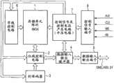
图1是表示作为适用于本实施方式的半导体存储装置的NAND闪存的一例的构成图。FIG. 1 is a configuration diagram showing an example of a NAND flash memory applied to the semiconductor memory device of the present embodiment.
图2是表示图1所示的存储单元阵列以及位线控制电路的构成的一例的电路图。FIG. 2 is a circuit diagram showing an example of the configuration of the memory cell array and the bit line control circuit shown in FIG. 1 .
图3是将图2所示的存储单元阵列的一部分取出来表示的电路图。FIG. 3 is a circuit diagram showing a part of the memory cell array shown in FIG. 2 .
图4是表示图3所示的电路的图案的俯视图。FIG. 4 is a plan view showing a pattern of the circuit shown in FIG. 3 .
图5A是存储单元的剖视图,图5B是选择门的剖视图。FIG. 5A is a cross-sectional view of a memory cell, and FIG. 5B is a cross-sectional view of a selection gate.
图6是与第一实施方式对应的半导体存储装置的剖视图。6 is a cross-sectional view of a semiconductor memory device corresponding to the first embodiment.
图7是表示图6的擦除、编程、读取时的各部的电压的图。FIG. 7 is a diagram showing voltages of each part during erasing, programming, and reading in FIG. 6 .
图8是表示图2所示的数据存储电路的一部分的图,是表示读出放大单元的电路图。FIG. 8 is a diagram showing a part of the data storage circuit shown in FIG. 2 , and is a circuit diagram showing a sense amplifier unit.
图9是表示图2所示的数据存储电路的一部分的图,是表示数据控制单元的电路图。FIG. 9 is a diagram showing a part of the data storage circuit shown in FIG. 2 , and is a circuit diagram showing a data control unit.
图10A、10B是概略表示写入到存储单元中的阈值电平的变化的图。10A and 10B are diagrams schematically showing changes in threshold levels written in memory cells.
图11是表示第一实施方式涉及的擦除顺序(sequence)的流程图。FIG. 11 is a flowchart showing an erasing sequence (sequence) according to the first embodiment.
图12是表示第一实施方式涉及的写入状态的选择用存储单元的电路图。12 is a circuit diagram showing a selection memory cell in a write state according to the first embodiment.
图13是概略表示第一实施方式涉及的写入顺序的流程图。FIG. 13 is a flowchart schematically showing a writing procedure according to the first embodiment.
图14是表示与字线连接的第偶数个存储单元的写入顺序的流程图。FIG. 14 is a flowchart showing a procedure for writing to an even-numbered memory cell connected to a word line.
图15是表示与字线连接的第奇数个存储单元的写入顺序的流程图。FIG. 15 is a flowchart showing a writing procedure for odd-numbered memory cells connected to word lines.
图16是表示编程顺序的变形例的流程图。FIG. 16 is a flowchart showing a modified example of the programming procedure.
图17A、17B是概略表示第一实施方式涉及的读取工作的流程图。17A and 17B are flowcharts schematically showing the reading operation according to the first embodiment.
图18是表示第二实施方式涉及的擦除顺序的流程图。FIG. 18 is a flowchart showing an erasing procedure according to the second embodiment.
图19是将第三实施方式涉及的存储单元阵列的一部分取出来表示的电路图。FIG. 19 is a circuit diagram showing a part of the memory cell array according to the third embodiment.
图20是表示图19所示的电路的图案的俯视图。FIG. 20 is a plan view showing a pattern of the circuit shown in FIG. 19 .
图21是将第四实施方式涉及的存储单元阵列的一部分取出来表示的电路图。FIG. 21 is a circuit diagram showing a part of the memory cell array according to the fourth embodiment.
图22是表示图21所示的电路的图案的俯视图。FIG. 22 is a plan view showing a pattern of the circuit shown in FIG. 21 .
具体实施方式Detailed ways
下面参照附图对实施方式进行说明。Embodiments are described below with reference to the drawings.
(第一实施方式)(first embodiment)
图1表示第一实施方式涉及的半导体存储装置的构成,示出了例如在存储单元中存储4值(2位)的NAND闪存。FIG. 1 shows the configuration of the semiconductor memory device according to the first embodiment, and shows, for example, a NAND flash memory in which 4 values (2 bits) are stored in memory cells.
存储单元阵列1包含多条位线、多条字线和共用源极线,例如呈矩阵状配置有包括EEPROM单元的能够电重写数据的存储单元。在该存储单元阵列1上连接有用于控制位线的位线控制电路2和字线控制电路6。The
位线控制电路2经由位线读取存储单元阵列1中的存储单元的数据,经由位线检测存储单元阵列1中的存储单元的状态,经由位线对存储单元阵列1中的存储单元施加写入控制电压来对存储单元进行写入。在位线控制电路2上连接有列译码器3、数据输入输出缓冲器4。位线控制电路2内的数据存储电路通过列译码器3来选择。读取到数据存储电路中的存储单元的数据,经由所述数据输入输出缓冲器4从数据输入输出端子5输出到外部。数据输入输出端子5与存储芯片外部的未图示的主机连接。该主机例如包括微型计算机,接收从所述数据输入输出端子5输出的数据。进而,主机输出控制NAND型闪存的工作的各种命令CMD、地址ADD以及数据DT。从主机输入到数据输入输出端子5的写入数据,经由数据输入输出缓冲器4被供给到由列译码器3选择出的数据存储电路,命令及地址被供给到控制信号及控制电压产生电路7。The bit
字线控制电路6连接于存储单元阵列1。该字线控制电路6选择存储单元阵列1中的字线,对所选择出的字线施加读取、写入或擦除所需要的电压。The word line control circuit 6 is connected to the
存储单元阵列1、位线控制电路2、列译码器3、数据输入输出缓冲器4以及字线控制电路6连接于控制信号及控制电压产生电路7,通过该控制信号及控制电压产生电路7来控制。控制信号及控制电压产生电路7连接于控制信号输入端子8,通过从主机经由控制信号输入端子8输入的控制信号ALE(地址锁存使能)、CLE(命令锁存使能)、WE(写使能)、RE(读使能)来控制。该控制信号及控制电压产生电路7在数据的写入时产生字线和/或位线的电压,并如后所述那样产生向阱(well)供给的电压。控制信号及控制电压产生电路7包含例如如电荷泵(charge pump)电路的升压电路,能够生成编程电压、读电压以及擦除电压等电压。The
所述位线控制电路2、列译码器3、字线控制电路6、控制信号及控制电压产生电路7构成写入电路和读取电路。The bit
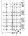
图2示出了图1所示的存储单元阵列1及位线控制电路2的构成的一例。存储单元阵列1具有多个NAND串NS。相邻的例如2个NAND串连接于1条位线BL0、BL1、BLi、BLn。这些位线BL0、BL1、BLi、BLn分别连接于构成位线控制电路2的数据存储电路10。数据存储电路10被供给地址信号(YA0、YA1、YAi、YAn)。FIG. 2 shows an example of the configuration of the
1个NAND串NS构成为串联连接例如128个存储单元MC、第一选择用存储单元SMO、第二选择用存储单元SME、选择门S1、S2。存储单元MC、第一选择用存储单元SMO和第二选择用存储单元SME例如由EEPROM构成。选择门S2连接于位线BL0(BL1、BLi、BLn),选择门S1连接于第一源极线SRC1(或第二源极线SRC2)。One NAND string NS is configured such that, for example, 128 memory cells MC, a first selection memory cell SMO, a second selection memory cell SME, and selection gates S1 and S2 are connected in series. The memory cell MC, the first selection memory cell SMO, and the second selection memory cell SME are formed of, for example, EEPROM. The selection gate S2 is connected to the bit line BL0 (BL1, BLi, BLn), and the selection gate S1 is connected to the first source line SRC1 (or the second source line SRC2).
配置于各行的存储单元MC的控制栅极共同连接于字线WL0~WL127。第一选择用存储单元SMO的控制栅极连接于选择线SGDO,第二选择用存储单元SME的控制栅极连接于选择线SGDE。另外,选择门S2共同连接于选择线SGD,选择门S1共同连接于选择线SGS。The control gates of memory cells MC arranged in each row are commonly connected to word lines WL0 to WL127 . The control gate of the first selection memory cell SMO is connected to the selection line SGDO, and the control gate of the second selection memory cell SME is connected to the selection line SGDE. In addition, the selection gate S2 is commonly connected to the selection line SGD, and the selection gate S1 is commonly connected to the selection line SGS.
如以虚线所示,存储单元阵列1包含多个块。各块包括多个NAND串NS,例如以该块为单位来擦除数据。As indicated by dotted lines, the
连接于1条位线的2个NAND串NS中,由第一选择用存储单元SMO、第二选择用存储单元SME选择1个NAND串而连接于位线。在连接于1条位线的一方的NAND串中,连接于1条字线的多个存储单元(以虚线包围的范围内的存储单元)构成1页,在另一方的NAND串中,连接于1条字线的剩余的多个存储单元也构成1页。Of the two NAND strings NS connected to one bit line, one NAND string is selected by the first selection memory cell SMO and the second selection memory cell SME, and is connected to the bit line. In one NAND string connected to one bit line, a plurality of memory cells connected to one word line (memory cells in the range surrounded by a dotted line) constitute one page, and in the other NAND string, connected to The remaining memory cells of one word line also constitute one page.
数据的写入、读取按每页来执行。即,在数据的写入或读取工作时,配置在行方向上的多个存储单元中的一半的存储单元连接于对应的位线。因此,对配置在行方向上的多个存储单元的每一半执行写入或读取工作。Data writing and reading are performed for each page. That is, half of the plurality of memory cells arranged in the row direction are connected to corresponding bit lines during a data write or read operation. Therefore, writing or reading work is performed on each half of the plurality of memory cells arranged in the row direction.
在写入、读取工作中,连接于数据存储电路10的位线BL0o、BL1o、BLio、BLno由地址(YA0、YA1、YAi、YAn)来选择。In writing and reading operations, the bit lines BL0o, BL1o, BLio, and BLno connected to the
数据的写入、读取以页为单位来进行。在1个单元存储1位的情况下使用1页,在1个单元存储2位的情况下使用2页,在1个单元存储3位的情况下使用3页,在1个单元存储4位的情况下使用4页。页由地址来切换。Data writing and reading are performed in units of pages. 1 page is used when 1 bit is stored in 1 cell, 2 pages are used when 2 bits are stored in 1 cell, 3 pages are used when 3 bits are stored in 1 cell, and 4 bits are stored in 1 cell 4 pages are used in case. Pages are switched by address.
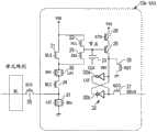
图3示出了图2所示的存储单元阵列1的一部分,图4示出了图3所示的电路的图案。参照图3、图4,对例如连接于位线BL1的NAND串NS1、NS2的构成进行进一步说明。其他NAND串的构成也与NAND串NS1、NS2是同样的。FIG. 3 shows a part of the
NAND串NS1、NS2分别构成为串联连接例如128个存储单元MC、第一选择用存储单元SMO、第二选择用存储单元SME、选择门S1、S2的源、漏扩散层(AA)。NAND串NS1、NS2的选择门S2的漏扩散层通过连接部11进行连接,在该连接部11经由通孔(或接触插塞)V1而连接于位线BL1。即,位线BL1经由通孔V1在连接部11与第一NAND串NS1、第二NAND串NS2连接。位线BL1例如由第一层金属布线层(M1)构成。The NAND strings NS1 and NS2 are configured such that, for example, 128 memory cells MC, first selection memory cells SMO, second selection memory cells SME, and source and drain diffusion layers (AA) of selection gates S1 and S2 are connected in series. The drain diffusion layers of the selection gates S2 of the NAND strings NS1 and NS2 are connected by the
另外,NAND串NS1的选择门S1的源扩散层通过连接部12与NAND串NS0的选择门S1的源扩散层连接,该连接部12连接于第二源极线SRC2。另外,NAND串NS2的选择门S1的源扩散层通过连接部13与NAND串NS3的选择门S1的源扩散层连接,该连接部13连接于第一源极线SRC1。In addition, the source diffusion layer of the selection gate S1 of the NAND string NS1 is connected to the source diffusion layer of the selection gate S1 of the NAND string NS0 through the connection portion 12 connected to the second source line SRC2. In addition, the source diffusion layer of the selection gate S1 of the NAND string NS2 is connected to the source diffusion layer of the selection gate S1 of the NAND string NS3 through the
图5A是存储单元MC、第一选择用存储单元SMO、第二选择用存储单元SME的剖视图,图5B示出了选择门S1、S2的剖视图。如图5A所示,第一选择用存储单元SMO、第二选择用存储单元SME为与存储数据的存储单元MC同样的构造。但是,为了与存储单元MC相比提高可靠性,第一选择用存储单元SMO、第二选择用存储单元SME的尺寸可以比存储单元MC的尺寸大。另外,在选择门S1、S2与第一选择用存储单元SMO、第二选择用存储单元SME之间、和第一选择用存储单元SMO、第二选择用存储单元SME与存储单元MC之间也可以配置虚设的单元。5A is a cross-sectional view of a memory cell MC, a first selection memory cell SMO, and a second selection memory cell SME, and FIG. 5B is a cross-sectional view of selection gates S1 and S2. As shown in FIG. 5A , the first selection memory cell SMO and the second selection memory cell SME have the same structure as the memory cell MC for storing data. However, in order to improve reliability compared with the memory cell MC, the size of the first selection memory cell SMO and the second selection memory cell SME may be larger than that of the memory cell MC. In addition, between the selection gates S1 and S2 and the first selection memory unit SMO and the second selection memory unit SME, and between the first selection memory unit SMO, the second selection memory unit SME and the memory cell MC are also Dummy units can be configured.
图6示出了NAND闪存的剖视图。例如在P型半导体基板51内形成有N型阱区域52、53、54、P型阱区域56。在N型阱区域52内形成有P型阱区域55,在该P型阱区域55内形成有构成存储单元阵列1的低电压N沟道晶体管LVNTr。进而,在所述N型阱区域53、P型阱区域56内形成有构成数据存储电路10的低电压P沟道晶体管LVPTr、低电压N沟道晶体管LVNTr。进而,在基板51内形成有连接位线与数据存储电路10的高电压N沟道晶体管HVNTr。另外,在N型阱区域54内形成有构成例如字线驱动电路等的高电压P沟道晶体管HVPTr。如图6所示,高电压晶体管HVNTr、HVPTr例如具有比低电压晶体管LVNTr、LVPTr厚的栅极绝缘膜。FIG. 6 shows a cross-sectional view of a NAND flash memory. For example, N-
此外,在图6中省略了第二源极线SRC2。In addition, the second source line SRC2 is omitted in FIG. 6 .
图7示出了向图6所示的各区域供给的电压的例子。在擦除、写入(也称为编程)、读取(也称为“读出”)中,向各区域供给如图7所示的电压。在此,Vera是在数据擦除时对基板施加的电压,Vss是接地电压,Vdd是电源电压。Vpgmh是在数据写入时对行译码器内的N沟道MOS晶体管的栅极施加的电压,是用于以与N沟道MOS晶体管的阈值电压相应而不降低的方式使字线的写入电压Vpgm通过的电位。也即是,Vpgmh为向字线供给的电压Vpgm+Vth(Vth:N沟道MOS晶体管的阈值电压)。Vreadh是在读取时对行译码器内的N沟道MOS晶体管的栅极施加的电压,是用于以与N沟道MOS晶体管的阈值电压相应而不降低的方式使Vread通过的电位。也即是,Vreadh为向字线供给的电压,在读取时为Vread+Vth(Vth:N沟道MOS晶体管的阈值电压)。FIG. 7 shows examples of voltages supplied to the respective regions shown in FIG. 6 . In erasing, writing (also referred to as programming), and reading (also referred to as “reading”), a voltage as shown in FIG. 7 is supplied to each region. Here, Vera is a voltage applied to the substrate when erasing data, Vss is a ground voltage, and Vdd is a power supply voltage. Vpgmh is the voltage applied to the gate of the N-channel MOS transistor in the row decoder when data is written, and is used to make the writing of the word line correspond to the threshold voltage of the N-channel MOS transistor without lowering it. The potential through which the input voltage Vpgm passes. That is, Vpgmh is the voltage Vpgm+Vth (Vth: threshold voltage of the N-channel MOS transistor) supplied to the word line. Vreadh is a voltage applied to the gate of the N-channel MOS transistor in the row decoder at the time of reading, and is a potential for passing Vread so as not to decrease in accordance with the threshold voltage of the N-channel MOS transistor. That is, Vreadh is the voltage supplied to the word line, and is Vread+Vth (Vth: threshold voltage of the N-channel MOS transistor) at the time of reading.
另外,在数据写入时,作为向非选择单元的字线供给的电压有Vpass,在数据读取时作为向非选择字线供给的电压有Vread。In addition, Vpass is the voltage supplied to the word line of the unselected cell at the time of data writing, and Vread is the voltage supplied to the unselected word line at the time of data reading.
图8、图9示出了图2所示的数据存储电路10的一例。数据存储电路10包括图8所示的读出放大单元(SAU)10a和图9所示的数据控制单元(DCU)10b。8 and 9 show an example of the
在图8中,读出放大单元10a包括多个N沟道MOS晶体管(以下称为NMOS)21~27、多个P沟道MOS晶体管(以下称为PMOS)28、29、传输门30、31、锁存电路32以及电容器33。锁存电路32例如包括时钟反相(clocked inverter)电路32a、32b构成。In FIG. 8, the
NMOS21的电流通路的一端连接于供给电源Vdd的节点,另一端经由传输门30、NMOS24、传输门31而接地。在NMOS24与传输门31的连接节点上连接有NMOS25的电流通路的一端。该NMOS25的另一端与配置于存储单元阵列的位线BL连接。在NMOS21上并联连接有NMOS22、23的串联电路。One end of the current path of
另外,PMOS28的电流通路的一端连接于供给电源Vdd的节点,另一端经由PMOS29与构成锁存电路32的反相电路32a的输入端连接,并经由NMOS26接地。与该反相电路32a交叉连接的时钟反相电路32b的输入端经由NMOS27与数据控制单元(DCU)10b连接。另外,PMOS29的栅极连接于NMOS22、23的连接节点,在该连接节点上连接有电容器33的一端。在该电容器33的另一端被供给时钟脉冲信号CLK。In addition, one end of the current path of the
在NMOS21的栅极被供给信号BLX。在构成传输门30的NMOS的栅极被供给构成锁存电路32的反相电路32a的输出端的信号LAT,在PMOS晶体管的栅极被供给反相电路32a的输入端的信号INV。在NMOS24的栅极被供给信号BLC,在NMOS25的栅极被供给信号BLS。A signal BLX is supplied to the gate of the
在NMOS22的栅极被供给信号HLL,在NMOS23的栅极被供给信号XXL。The signal HLL is supplied to the gate of the
在PMOS28的栅极被供给信号STB,在NMOS26的栅极被供给复位信号RST。在NMOS27的栅极被供给信号NCO。The signal STB is supplied to the gate of the
概略说明上述读出放大单元的工作。The operation of the above-mentioned sense amplifier unit will be briefly described.
(写入工作)(write job)
在向存储单元写入数据的情况下,首先,使信号STB为高电平(以下记为H电平),使复位信号RST暂且为H电平,锁存电路32被复位而使LAT为H电平,使信号INV为低电平(以下记为L电平)。In the case of writing data to a memory cell, first, the signal STB is set to a high level (hereinafter referred to as an H level), the reset signal RST is temporarily set to an H level, and the
然后,使信号NCO为H电平,从数据控制单元10b取入数据。在该数据为表示写入的L电平(“0”)的情况下,信号LAT成为L电平,信号INV成为H电平。另外,在数据为表示非写入的H电平(“1”)的情况下,锁存电路32的数据不改变,LAT保持为H电平,信号INV保持为L电平。Then, the signal NCO is set to H level, and data is taken in from the
接着,当使信号BLX、BLC、BLS为H电平时,锁存电路的信号LAT为L电平、信号INV为H电平(写入)的情况下,传输门30断开而传输门31接通,位线BL成为Vss。在该状态下,当字线成为编程电压Vpgm时,数据被写入到存储单元。Next, when the signals BLX, BLC, and BLS are at the H level, when the signal LAT of the latch circuit is at the L level and the signal INV is at the H level (writing), the
另一方面,在锁存电路32中,信号LAT为H电平、信号INV为L电平(非写入)的情况下,由于传输门30接通(on)而传输门31断开(off),所以位线BL被充电至Vdd。因此,在字线变为了Vpgm的情况下,由于单元的沟道被升压到高的电位,所以数据没有被写入存储单元。On the other hand, in the
(读取工作、编程校验读取工作)(read work, programming verification read work)
在从存储单元读取数据的情况下,首先,使设置信号RST暂且为H电平,锁存电路32被复位,使信号LAT为H电平,使信号INV为L电平。然后,使信号BLS、BLC、BLX、HLL、XXL为预定的电压,位线BL被充电。随着上述动作,电容器33的节点被充电至Vdd。在此,在存储单元的阈值电压比读取电平高的情况下,存储单元为断开状态(截止状态),位线保持为H电平。也即是,节点保持为H电平。另外,在存储单元的阈值电压比读取电平低的情况下,存储单元成为接通状态(导通状态),位线BL的电荷被放电。因此,位线BL成为L电平。因此,节点(Node)成为L电平。When reading data from a memory cell, first, set signal RST is temporarily set to H level,
接着,当使信号STB为L电平时,在存储单元接通的情况下,由于节点为L电平,所以PMOS29导通,锁存电路32的信号INV成为H电平,信号LAT成为L电平。另一方面,在存储单元断开(截止)的情况下,锁存电路32的信号INV保持为L电平,信号LAT被称为H电平。Next, when the signal STB is at L level, when the memory cell is turned on, since the node is at L level, the
然后,当使信号NCO为H电平时,NMOS27导通,锁存电路32的数据被传送给数据控制单元10b。Then, when the signal NCO is set at H level, the
在写入工作后,验证存储单元的阈值电压的编程校验工作与上述读取工作大致同样。After the write operation, the program verification operation for verifying the threshold voltage of the memory cell is substantially the same as the above-mentioned read operation.
图9示出了数据控制单元(DCU)10b的一例。FIG. 9 shows an example of a data control unit (DCU) 10b.
图9所示的数据控制单元10b包括运算电路40和多个数据锁存电路ADL、BDL、XDL及NMOS41。The data control
运算电路40包括总线(以下记为IBUS)、与IBUS的两端连接而互补地进行工作的传输门42、43、锁存IBUS的数据的锁存电路44、以及根据该锁存电路44的数据设定数据锁存电路ADL、BDL、XDL的电平的设定电路45。The
传输门42根据互补的信号COND和信号CONS进行工作,连接读出放大单元SAU10a的总线(记为SBUS)和IBUS。传输门43根据互补的信号CONS和信号COND进行工作,连接IBUS和与数据锁存电路ADL、BDL、XDL连接的总线(以下记为DBUS)。在传输门42接通时,传输门43断开,在传输门42断开时,传输门43接通。The
锁存电路44包括多个PMOS46~49、多个NMOS50~56以及反相电路68。在PMOS46和NMOS50的栅极被供给设置信号SET,在PMOS48的栅极被供给复位信号REST。在NMOS53的栅极被供给信号IFH,在NMOS55的栅极被供给信号IFL。NMOS54的栅极经由反相电路68与IBUS连接,NMOS56的栅极与IBUS连接。The
设定电路45包括PMOS57~60和NMOS61~64。在PMOS57的栅极以及NMOS61的栅极被供给信号FAIL。该信号FAIL是作为锁存电路44的一方的输出端的PMOS47与NMOS51的连接节点的信号。在PMOS59和NMOS63的栅极供给信号MTCH。该信号MTCH是作为锁存电路44的另一方的输出端的PMOS49与NMOS52的连接节点的信号。进而,在PMOS58的栅极被供给信号M2HB,在PMOS60的栅极被供给信号F2HB。在NMOS62的栅极被供给F2L,在NMOS64的栅极被供给信号M2L。The setting
数据锁存电路ADL、BDL、XDL为相同的构成,包括锁存电路66和将该锁存电路66连接于DBUS的传输门65。各传输门65通过信号BLCA、BLCA_B、BLCB、BLCB_B、BLCX、BLCX_B来控制。数据锁存电路XDL经由NMOS41与外部的IO连接。在NMOS41的栅极被供给信号CSL。The data latch circuits ADL, BDL, and XDL have the same configuration, and include a
如上所述,数据控制单元10b在保持写入数据并且进行读取时,对从存储单元读取的数据进行保持。As described above, the
从数据输入输出缓冲器6供给的例如2位的写入数据,经由数据锁存电路XDL被一位一位地锁存在例如数据锁存电路ADL、BDL中。For example, 2-bit write data supplied from the data input/output buffer 6 is latched bit by bit in, for example, the data latch circuits ADL, BDL via the data latch circuit XDL.
图9所示的运算电路40能够对数据锁存电路ADL、BDL的数据执行“与”、“或”、“异或非”等运算。例如在“与”的情况下,保持在数据锁存电路ADL、BDL中的数据被输出到DBUS以及IBUS。在该情况下,仅在保持在数据锁存电路ADL、BDL中的数据都为“1”的情况下,IBUS才成为H电平,在其他情况下,IBUS成为L电平。即,仅在非写入时IBUS变为“1”,在写入时IBUS变为“0”。通过将该数据经由SBUS传送到图8所示的读出放大单元10a来进行写入。The
运算电路40的工作可以进行各种变形,例如1个逻辑运算也可以适用各种各样的控制方法,可以根据需要来改变控制方法。The operation of the
图10A、10B示出了2位4值的第一、第二页写入后的存储单元的数据、阈值电压、校验电平和读取电平。10A and 10B show the data, threshold voltage, verification level and read level of the memory cells after the first and second pages of 2-bit 4-value are written.
如图10A所示,通过擦除工作,存储单元的数据变为“11”的阈值电压。通过第一页的数据被写入,存储单元维持擦除状态或被电平LMV写入,存储单元的数据变为“11”或“10”的阈值电压。As shown in FIG. 10A, the data of the memory cell becomes a threshold voltage of "11" by the erase operation. After the data of the first page is written, the memory cell maintains the erased state or is written with the level LMV, and the data of the memory cell becomes a threshold voltage of "11" or "10".
如图10B所示,通过第二页的数据被写入,存储单元维持擦除状态或被AV、BV、CV的任一方的电平写入,存储单元的数据变为“11”、“01”、“00”、“10”的阈值。对于写入时的校验电平,为了使之具有数据保留余裕(retention margin),因此被设定为比读取时的电平稍高的电平。在图10A、10B中,读取电平由“LMR、AR、BR、CR”来表示,校验读取电平由“LMV、AV、BV、CV”来表示。As shown in Figure 10B, when the data of the second page is written, the memory cell maintains the erased state or is written at any level of AV, BV, and CV, and the data of the memory cell becomes "11", "01" ", "00", "10" thresholds. The verify level at the time of writing is set to a level slightly higher than the level at the time of reading in order to have a data retention margin. In FIGS. 10A and 10B , the read levels are represented by "LMR, AR, BR, CR", and the verify read levels are represented by "LMV, AV, BV, CV".
(擦除顺序)(erasing order)
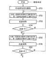
参照图11、图12对本实施方式涉及的擦除顺序进行说明。The erasing sequence according to this embodiment will be described with reference to FIGS. 11 and 12 .
在擦除工作中,首先,将选择块(BLK)的全部字线WL0~WL127和与第一、第二选择用存储单元连接的选择线SGDO、SGDE设定成0V,将非选择块的全部字线、选择线SGDO、SGDE设定为浮置状态,将形成有存储单元阵列1的阱设定成擦除电压VERA。由此,选择块内的存储单元及第一选择用存储单元SMO、第二选择用存储单元SME全部变为擦除状态(ST11)。In the erasing operation, first, all the word lines WL0~WL127 of the selected block (BLK) and the selection lines SGDO and SGDE connected to the first and second selection memory cells are set to 0V, and all the word lines of the non-selected block are set to 0V. The word lines and the selection lines SGDO and SGDE are set to a floating state, and the wells in which the
然后,为了能够任意地选择与选择块内的各位线连接的2个NAND串中的一方,第一选择用存储单元SMO和第二选择用存储单元SME被选择性地写入。Then, the first memory cell for selection SMO and the second memory cell for selection SME are selectively written so that one of the two NAND strings connected to the bit lines in the selected block can be arbitrarily selected.
在例如将图12所示的与1条位线BL1连接的2个NAND串定义为第一NAND串NS1、第二NAND串NS2的情况下,将第一NAND串NS1的第一选择用存储单元SMO设定为写入状态,将第二选择用存储单元SME设定为非写入状态,将第二NAND串NS2的第一选择用存储单元SMO设定为非写入状态,将第二选择用存储单元SME设定为写入状态。For example, when two NAND strings connected to one bit line BL1 shown in FIG. 12 are defined as a first NAND string NS1 and a second NAND string NS2, the first selection memory cell of the first NAND string NS1 SMO is set to the writing state, the second selection memory cell SME is set to the non-writing state, the first selection memory cell SMO of the second NAND string NS2 is set to the non-writing state, and the second selection memory cell SMO is set to the non-writing state. Set the write state with the memory cell SME.
具体而言,首先,选择性地对选择块内的第二NAND串NS2的第二选择用存储单元SME进行写入,使阈值电压上升。此时,第一选择用存储单元SMO成为非写入。另外,第一NAND串NS1的第一选择用存储单元SMO及第二选择用存储单元SME也成为非写入(ST12)。因此,第一源极线SRC1被设定为例如Vss(接地电压),第二源极线SRC2被设定为Vdd(电源电压),选择线SGD被设定为Vss,选择线SGS被设定为VSGD(Vdd+Vth,Vth为NMOS晶体管的阈值电压),与第二选择用存储单元SME连接的选择线SGDE被设定为Vpgm(编程电压),与第一选择用存储单元SMO连接的选择线SGDO被设定为Vpass(中间电压),全部字线WL0~WL127被设定为Vpass,第二选择用存储单元SME被进行写入。Specifically, first, writing is selectively performed in the second selected memory cell SME of the second NAND string NS2 in the selected block to increase the threshold voltage. At this time, the first selection memory cell SMO is not written. In addition, the first selection memory cell SMO and the second selection memory cell SME of the first NAND string NS1 are also non-writing ( ST12 ). Therefore, the first source line SRC1 is set to, for example, Vss (ground voltage), the second source line SRC2 is set to Vdd (power supply voltage), the selection line SGD is set to Vss, and the selection line SGS is set to VSGD (Vdd+Vth, Vth is the threshold voltage of the NMOS transistor), the selection line SGDE connected to the second selection memory cell SME is set to Vpgm (programming voltage), and the selection line SGDE connected to the first selection memory cell SMO Line SGDO is set to Vpass (intermediate voltage), all word lines WL0 to WL127 are set to Vpass, and second selection memory cell SME is written.
接着,选择性地对选择块内的第一NAND串NS1的第一选择用存储单元SMO进行写入,使阈值电压上升。此时,第二选择用存储单元SME成为非写入。第二NAND串NS2的第一选择用存储单元SMO以及第二选择用存储单元SME也成为非写入(ST13)。因此,第一源极线SRC1被设定为Vdd,第二源极线SRC2被设定为Vss,选择线SGD被设定为Vss,选择线SGS被设定为VSGD,与第二选择用存储单元SME连接的选择线SGDE被设定为Vpass,与第一选择用存储单元SMO连接的选择线SGDO被设定为Vpgm,全部字线WL0~WL127被设定为Vpass,第一选择用存储单元SMO被进行写入。Next, writing is selectively performed in the first selection memory cell SMO of the first NAND string NS1 in the selected block to increase the threshold voltage. At this time, the second memory cell SME for selection is non-writing. The first selection memory cell SMO and the second selection memory cell SME of the second NAND string NS2 also become non-writing ( ST13 ). Therefore, the first source line SRC1 is set to Vdd, the second source line SRC2 is set to Vss, the selection line SGD is set to Vss, the selection line SGS is set to VSGD, and the second selection memory The selection line SGDE connected to the cell SME is set to Vpass, the selection line SGDO connected to the first selection memory cell SMO is set to Vpgm, all word lines WL0 to WL127 are set to Vpass, and the first selection memory cell SMO is set to Vpass. SMO is written.
被进行了写入的第二NAND串NS2的第二选择用存储单元SME以及第一NAND串NS1的第一选择用存储单元SMO的阈值电压,例如被设定为大于等于图10A所示的阈值电平“LMV”。The threshold voltages of the second selected memory cell SME of the second NAND string NS2 and the first selected memory cell SMO of the first NAND string NS1 that have been written are set to be equal to or greater than the threshold shown in FIG. 10A , for example. Level "LMV".
在图12中,由虚线包围的第一选择用存储单元SMO、第二选择用存储单元SME为写入状态,除此以外的第一选择用存储单元SMO、第二选择用存储单元SME为非写入状态(擦除状态)。即,第一选择用存储单元SMO、第二选择用存储单元SME沿着行方向按每2个被交替地写入。In FIG. 12 , the first selection memory cell SMO and the second selection memory cell SME surrounded by a dotted line are in the writing state, and the other first selection memory cells SMO and the second selection memory cell SME are in the non-write state. Write state (erase state). That is, the first selection memory cell SMO and the second selection memory cell SME are alternately written every two along the row direction.
通过如此设定第一选择用存储单元SMO、第二选择用存储单元SME的阈值电压,能够通过选择线SGDO、SGDE的电位来选择与1条位线连接的2个NAND串的一方。By setting the threshold voltages of the first selection memory cell SMO and the second selection memory cell SME in this way, one of the two NAND strings connected to one bit line can be selected by the potential of the selection lines SGDO and SGDE.
在本实施方式中,在选择块的擦除时将选择用存储单元擦除,然后进行写入工作,但也可以为如下动作:在出厂前的工序中对全部块的选择存储单元进行写入工作并设定为预定的存储单元的阈值电压,在出厂后的块擦除时不擦除选择存储单元的阈值。如此,能够在各块擦除时节省选择用存储单元的写入工作。In this embodiment, when erasing the selected block, the memory cells for selection are erased, and then the writing operation is performed, but the operation may be as follows: the selected memory cells of all the blocks are written in the process before shipment. It works and is set to the predetermined threshold voltage of the memory cell, and does not erase the threshold voltage of the selected memory cell during block erase after shipment. In this way, it is possible to save writing work in memory cells for selection when erasing each block.
进而,如此在出厂前的工序中对全部块的选择存储单元进行写入并设定为预定的阈值电压,并在出厂后的块擦除时不擦除选择存储单元的阈值电压的情况下,也可以:在各块擦除时检查选择存储单元的阈值电压,当阈值电压不为预定的电平时,将选择存储单元擦除并进行写入,将选择存储单元的阈值电压设定为预定的阈值电平。Furthermore, when the selected memory cells of all blocks are written and set to a predetermined threshold voltage in the pre-shipment process, and the threshold voltage of the selected memory cells is not erased when the block is erased after shipment, It is also possible to: check the threshold voltage of the selected memory cell when each block is erased, and when the threshold voltage is not at a predetermined level, erase and write the selected memory cell, and set the threshold voltage of the selected memory cell to a predetermined level. threshold level.
(编程顺序)(programming sequence)
在如上述那样结束了擦除顺序之后,能够对存储单元进行数据的写入。数据的写入按从接近第一源极线SRC1、第二源极线SRC2的字线WL0向接近位线的字线WL127的顺序来执行。After the erase sequence is completed as described above, data can be written into the memory cell. Writing of data is performed in order from the word line WL0 close to the first source line SRC1 and the second source line SRC2 to the word line WL127 close to the bit line.
另外,选择与1条位线连接的2个NAND串的一方来写入数据。在此,将图12所示的NAND串NS0、NS1、NS4、NS5……所包含的存储单元定位为第奇数个存储单元,将NAND串NS2、NS3……所包含的存储单元定义为第偶数个存储单元。Also, one of the two NAND strings connected to one bit line is selected to write data. Here, the memory cells contained in the NAND strings NS0, NS1, NS4, NS5... shown in Figure 12 are positioned as the odd-numbered memory cells, and the memory cells contained in the NAND strings NS2, NS3... storage unit.
图13概略性地示出了在向1个存储单元写入2位的情况下的编程顺序。FIG. 13 schematically shows a program sequence in the case of writing 2 bits into one memory cell.
对于写入,考虑相邻的存储单元的耦合电容来执行该写入。因此,首先,对与字线WL0连接的第偶数个(NS2、NS3……)存储单元执行第一页的编程顺序(ST21)。编程顺序包含数据的写入(编程)以及写入校验(编程校验读取)。在写入后进行写入校验,在写入不充分的情况下,再次进行写入,通过反复进行写入以及写入校验,对存储单元设定预定的阈值电压。For writing, the writing is performed in consideration of the coupling capacitance of adjacent memory cells. Therefore, first, the programming sequence of the first page is performed on the even-numbered (NS2, NS3 . . . ) memory cells connected to the word line WL0 ( ST21 ). The programming sequence includes writing of data (programming) and writing verification (programming verification reading). Write verification is performed after writing, and when writing is insufficient, writing is performed again, and by repeating writing and writing verification, a predetermined threshold voltage is set in the memory cell.
接着,对与字线WL0连接的第奇数个(NS0、NS1、NS4、NS5……)存储单元执行第一页的编程顺序(ST22)。然后,对与相邻的字线WL1连接的第偶数个(NS2,NS3……)存储单元执行第一页的编程顺序(ST23)。接着,对与字线WL1连接的第奇数个(NS0、NS1、NS4、NS5……)存储单元执行第一页的编程顺序(ST24)。Next, the program sequence of the first page is performed on the odd-numbered (NS0, NS1, NS4, NS5 . . . ) memory cells connected to the word line WL0 ( ST22 ). Then, the programming sequence of the first page is performed on the even-numbered (NS2, NS3 . . . ) memory cells connected to the adjacent word line WL1 ( ST23 ). Next, the programming sequence of the first page is performed on the odd-numbered (NS0, NS1, NS4, NS5 . . . ) memory cells connected to the word line WL1 ( ST24 ).
然后,对与字线WL0连接的第偶数个(NS2、NS3……)存储单元执行第二页的编程顺序(ST25)。接着,对与字线WL0连接的第奇数个(NS0、NS1、NS4、NS5……)存储单元执行第二页的编程顺序(ST26)。然后,对与字线WL2连接的第偶数个(NS2、NS3……)存储单元执行第一页的编程顺序(ST27)。进一步,对与字线WL2连接的第奇数个(NS0、NS1、NS4、NS5……)存储单元执行第一页的编程顺序(ST28)。如此来控制写入。Then, the programming sequence of the second page is performed on the even-numbered (NS2, NS3 . . . ) memory cells connected to the word line WL0 ( ST25 ). Next, the program sequence of the second page is performed on the odd-numbered (NS0, NS1, NS4, NS5 . . . ) memory cells connected to the word line WL0 ( ST26 ). Then, the programming sequence of the first page is performed on the even-numbered (NS2, NS3 . . . ) memory cells connected to the word line WL2 ( ST27 ). Further, the programming sequence of the first page is performed on the odd-numbered (NS0, NS1, NS4, NS5 . . . ) memory cells connected to the word line WL2 ( ST28 ). This is how to control writing.
此外,图13示出了向1个存储单元存储2位的情况,但在向1个存储单元存储1位的情况下,例如接着图13所示的步骤ST21~ST24的写入,对步骤27所示的与字线WL2连接的第奇数个(NS0、NS1、NS4、NS5……)存储单元执行第一页的编程顺序(sequence,程序)。也即是,跳过图13的第二页的写入,仅进行第一页的写入。In addition, FIG. 13 shows the case of storing 2 bits in one memory cell, but in the case of storing 1 bit in one memory cell, for example, subsequent to the writing of steps ST21 to ST24 shown in FIG. 13 , the
通过这样的工作,能够向1个存储单元写入1位。Through such an operation, one bit can be written to one memory cell.
(与字线WL0连接的第偶数个(NS2、NS3……)存储单元的写入顺序)(The writing order of the even-numbered (NS2, NS3...) memory cells connected to the word line WL0)
图14示出了与字线WL0连接的第偶数个(NS2、NS3……)存储单元的写入顺序的例子。FIG. 14 shows an example of the writing order of the even-numbered (NS2, NS3 . . . ) memory cells connected to the word line WL0.
向存储单元写入的数据中的1页量的数据,被存储在构成图9所示的数据存储电路10的数据锁存电路XDL中。One page of data written in the memory cells is stored in the data latch circuit XDL constituting the
首先,对选择块内的全部NAND串进行充电(ST21-1)。First, all the NAND strings in the selected block are charged (ST21-1).
该情况下,选择线SGD被设定为VSGD,选择线SGS被设定为Vss,选择线SGDE、SGDO被设定为VON(能够使写入状态的第一选择用存储单元SMO、第二选择用存储单元SME为接通状态的电压,例如Vread),位线被设定为Vdd。In this case, the selection line SGD is set to VSGD, the selection line SGS is set to Vss, and the selection lines SGDE and SGDO are set to VON (the first selection memory cell SMO and the second selection memory cell in the writing state can be set to VON). With the voltage at which the memory cell SME is on, eg Vread), the bit line is set to Vdd.
接着,将包含第偶数个存储单元的写入对象NAND串连接于位线(ST21-2)。Next, the NAND string to be written including the even-numbered memory cell is connected to the bit line ( ST21 - 2 ).
该情况下,选择线SGD被设定为VSGD,选择线SGS被设定为Vss,选择线SGDE被设定为VON,选择线SGDO被设定为VOFF(使写入状态的第一、第二选择用存储单元SMO为断开状态的电压,例如Vss)。位线在写入数据为“1”的情况下被设定为Vdd,在写入数据为“0”的情况下被设定为Vss。In this case, the selection line SGD is set to VSGD, the selection line SGS is set to Vss, the selection line SGDE is set to VON, and the selection line SGDO is set to VOFF (the first and second The selection memory cell SMO is an off-state voltage, for example, Vss). The bit line is set to Vdd when the write data is "1", and is set to Vss when the write data is "0".
然后,将第一源极线SRC1设定为VthD(例如耗尽型的NMOS晶体管的阈值电压),将第二源极线SRC2设定为Vdd,对字线WL0施加编程电压Vpgm,对非选择的字线施加Vpass(ST21-3)。如此,数据被写入到与字线WL0连接的第偶数个存储单元中。然后,执行未图示的编程校验,在比目的阈值电压低的情况下再次执行写入工作。Then, the first source line SRC1 is set to VthD (for example, the threshold voltage of a depletion-type NMOS transistor), the second source line SRC2 is set to Vdd, and the programming voltage Vpgm is applied to the word line WL0. Vpass is applied to the word line (ST21-3). In this way, data is written into the even-numbered memory cells connected to word line WL0. Then, program verify (not shown) is performed, and write operation is performed again when the voltage is lower than the target threshold voltage.
(与字线WL0连接的第奇数个(NS0、NS1、NS4、NS5……)存储单元的写入顺序)(The writing order of the odd-numbered (NS0, NS1, NS4, NS5...) memory cells connected to the word line WL0)
另一方面,图15示出了与字线WL0连接的第奇数个存储单元的写入顺序的例子。On the other hand, FIG. 15 shows an example of the writing order of odd-numbered memory cells connected to word line WL0.
首先,与第偶数个存储单元的写入同样,对选择块内的全部NAND串进行充电(ST22-1)。First, all the NAND strings in the selected block are charged ( ST22 - 1 ) in the same manner as the writing in the even-numbered memory cells.
该情况下,选择线SGD被设定为VSGD,选择线SGS被设定为Vss,选择线SGDE、SGDO被设定为VON,位线被设定为Vdd。In this case, the select line SGD is set to VSGD, the select line SGS is set to Vss, the select lines SGDE and SGDO are set to VON, and the bit line is set to Vdd.
接着,将包含第奇数个存储单元的写入对象NAND串连接于位线(ST22-2)。Next, the NAND string to be written including the odd-numbered memory cells is connected to the bit line ( ST22 - 2 ).
该情况下,选择线SGD被设定为VSGD,选择线SGS被设定为Vss,选择线SGDE被设定为VOFF,选择线SGDO被设定为VON。位线在写入数据为“1”的情况下被设定为Vdd,在写入数据为“0”的情况下被设定为Vss。In this case, the selection line SGD is set to VSGD, the selection line SGS is set to Vss, the selection line SGDE is set to VOFF, and the selection line SGDO is set to VON. The bit line is set to Vdd when the write data is "1", and is set to Vss when the write data is "0".
然后,将第一源极线SRC1设定为VthD(例如耗尽型的NMOS晶体管的阈值电压),将第二源极线SRC2设定为Vdd,对字线WL0施加编程电压Vpgm,对非选择的字线施加Vpass(ST22-3)。如此,向与字线WL0连接的第奇数个存储单元写入数据。然后,执行未图示的编程校验,在比目的阈值电压低的情况下再次执行写入工作。Then, the first source line SRC1 is set to VthD (for example, the threshold voltage of a depletion-type NMOS transistor), the second source line SRC2 is set to Vdd, and the programming voltage Vpgm is applied to the word line WL0. Vpass is applied to the word line (ST22-3). In this way, data is written into the odd-numbered memory cells connected to word line WL0. Then, program verify (not shown) is performed, and write operation is performed again when the voltage is lower than the target threshold voltage.
(编程顺序的变形例)(Modification of programming sequence)
在图13所示的编程顺序的情况下,由于在对第偶数个存储单元进行了写入之后,对第奇数个存储单元进行写入,所以先被写入的第偶数个存储单元的阈值电压有可能会变动。In the case of the programming sequence shown in Figure 13, since the odd-numbered memory cells are written after the even-numbered memory cells are written, the threshold voltage of the first even-numbered memory cells Subject to change.
图16表示在向1个存储单元写入2位的情况下的编程顺序的变形例。FIG. 16 shows a modified example of the program sequence when writing 2 bits into one memory cell.
该变形例中,在1个编程顺序中执行第偶数个(NS2、NS3、……)存储单元的编程、第奇数个(NS0、NS1、NS4、……)存储单元的编程、第偶数个(NS2、NS3、……)存储单元的编程校验读取以及第奇数个(NS0、NS1、NS4、……)存储单元的编程校验读取,在写入后进行写入校验,在写入不充分的情况下再次进行写入,通过反复进行写入以及写入校验来在预定的阈值电压写入1条字线的数据,然后执行下一条字线的编程顺序。In this modified example, the programming of the even-numbered (NS2, NS3, ...) memory cells, the programming of the odd-numbered (NS0, NS1, NS4, ...) memory cells, and the even-numbered ( NS2, NS3, ...) memory cell programming verification reading and odd-numbered (NS0, NS1, NS4, ...) memory cell programming verification reading, write verification after writing, after writing If the input is insufficient, write again, and write data for one word line at a predetermined threshold voltage by repeating write and write verify, and then execute the program sequence for the next word line.
即,对与字线WL0连接的存储单元执行第一页的上述编程顺序(ST31),然后,对与字线WL1连接的存储单元执行第一页的上述编程顺序(ST32)。接着,对与字线WL0连接的存储单元执行第二页的上述编程顺序(ST33),然后,对与字线WL2连接的存储单元执行第一页的上述编程顺序(ST34)。然后,对与字线WL1连接的存储单元执行第二页的上述编程顺序(ST35)。That is, the above-mentioned programming sequence of the first page is performed on the memory cells connected to the word line WL0 ( ST31 ), and then the above-mentioned programming sequence of the first page is performed on the memory cells connected to the word line WL1 ( ST32 ). Next, the above-mentioned programming sequence for the second page is performed on the memory cells connected to the word line WL0 ( ST33 ), and then the above-mentioned programming sequence for the first page is performed on the memory cells connected to the word line WL2 ( ST34 ). Then, the above-described program sequence of the second page is performed on the memory cells connected to the word line WL1 ( ST35 ).
通过设为这样的编程顺序,能够防止存储单元的阈值电压的变动。By adopting such a program sequence, it is possible to prevent fluctuations in the threshold voltage of memory cells.
此外,图16示出了向1个存储单元写入2位的情况下的编程顺序,而在向1个存储单元写入1位的情况下,例如在执行了图16所示的步骤ST31、ST32之后,对步骤ST34所示的与字线WL2连接的存储单元执行第一页的上述编程顺序。In addition, FIG. 16 shows the programming sequence in the case of writing 2 bits to 1 memory cell, and in the case of writing 1 bit to 1 memory cell, for example, after performing steps ST31, After ST32, the above-mentioned programming sequence of the first page is performed on the memory cells connected to the word line WL2 shown in step ST34.
通过这样的工作,能够向1个存储单元写入1位。Through such an operation, one bit can be written to one memory cell.
(读取工作)(read job)
图17A、17B示出了读取工作。17A, 17B show the read operation.
读取工作与写入工作同样地,对与字线连接的第偶数个存储单元和第奇数个存储单元分别进行读取。In the read operation, similarly to the write operation, the even-numbered memory cells and the odd-numbered memory cells connected to the word line are respectively read.
如图17A所示,在读取第偶数个存储单元的数据的情况下,将选择线SGD和选择线SGS设定为VSG,将选择线SGDE设定为VON,将选择线SGDO设定为VOFF,对位线施加预定的电位VBL。进一步,将第一源极线SRC1、第二源极线SRC2一起设定为VSRC(例如1V)。另外,如图10A、10B所示,选择字线根据所读取的数据而被设定为读取电平“LMR”、“AR”、“BR”、“CR”中的任一方。另外,将非选择的字线设定为Vread,执行读取工作(ST41)。As shown in Figure 17A, in the case of reading the data of the even-numbered memory cell, the selection line SGD and the selection line SGS are set to VSG, the selection line SGDE is set to VON, and the selection line SGDO is set to VOFF , a predetermined potential VBL is applied to the bit line. Furthermore, both the first source line SRC1 and the second source line SRC2 are set to VSRC (for example, 1V). In addition, as shown in FIGS. 10A and 10B , the selected word line is set to any one of the read levels “LMR”, “AR”, “BR”, and “CR” according to the read data. In addition, the unselected word line is set to Vread, and a read operation is performed ( ST41 ).
在存储单元的阈值电压比字线的电平低的情况下,存储单元变为接通,位线的电位变为低电平,在存储单元的阈值电压比字线的电平高的情况下,存储单元变为断开,位线的电位保持为高电平。该位线的电压由数据存储电路10来读取。When the threshold voltage of the memory cell is lower than the level of the word line, the memory cell is turned on and the potential of the bit line becomes low, and when the threshold voltage of the memory cell is higher than the level of the word line , the memory cell is turned off, and the potential of the bit line remains high. The voltage of this bit line is read by the
另一方面,在读取第奇数个存储单元的数据的情况下,将选择线SGD和选择线SGS设定为VSG,将选择线SGDE设定为VOFF,将选择线SGDO设定为VON,对位线施加预定的电位VBL。进一步,将第一源极线SRC1、第二源极线SRC2一起设定为VSRC。另外,如图10A、10B所示,选择字线根据所读取的数据而被设定为读取电平“LMR”、“AR”、“BR”、“CR”中的任一方。另外,将非选择的字线设定为Vread,执行读取工作(ST42)。On the other hand, in the case of reading the data of the odd-numbered memory cell, the selection line SGD and the selection line SGS are set to VSG, the selection line SGDE is set to VOFF, and the selection line SGDO is set to VON. A predetermined potential VBL is applied to the bit line. Furthermore, both the first source line SRC1 and the second source line SRC2 are set as VSRC. In addition, as shown in FIGS. 10A and 10B , the selected word line is set to any one of the read levels “LMR”, “AR”, “BR”, and “CR” according to the read data. In addition, the non-selected word line is set to Vread, and a read operation is performed ( ST42 ).
如上所述来读取第偶数个和第奇数个存储单元的数据。Data of the even-numbered and odd-numbered memory cells is read as described above.
根据上述第一实施方式,相邻的2个NAND串通过1个通孔与位线连接。因此,能够削减通孔的数量,即使在单元微细化的情况下,也能够将相邻的2个NAND串连接于位线。According to the first embodiment described above, two adjacent NAND strings are connected to the bit line through one via hole. Therefore, the number of via holes can be reduced, and two adjacent NAND strings can be connected to a bit line even when the cell is miniaturized.
另外,各NAND串分别具有第一选择用存储单元SMO、第二选择用存储单元SME。因此,能够通过第一选择用存储单元SMO、第二选择用存储单元SME使相邻的2个NAND串中的一方为选择状态,使另一方为非选择状态,能够选择2个NAND串中的一方或另一方。In addition, each NAND string has a first selection memory cell SMO and a second selection memory cell SME. Therefore, one of the two adjacent NAND strings can be in the selected state and the other can be in the non-selected state by the first selection memory cell SMO and the second selection memory cell SME, and one of the two NAND strings can be selected. one side or the other.
进而,相邻的2个NAND串中的一方的NAND串连接于第一源极线,另一方的NAND串连接于第二源极线。因此,能够选择性地对相邻的2个NAND串的第一选择用存储单元SMO、第二选择用存储单元SME进行写入。Furthermore, one of the two adjacent NAND strings is connected to the first source line, and the other NAND string is connected to the second source line. Therefore, it is possible to selectively write to the first memory cell for selection SMO and the second memory cell for selection SME of two adjacent NAND strings.
另外,如图13所示,交替地选择第一NAND串NS1、第二NAND串NS2,从源极线SRC1、SRC2侧的存储单元依次进行写入。因此,能够防止存储单元的阈值电压的变动。In addition, as shown in FIG. 13 , the first NAND string NS1 and the second NAND string NS2 are alternately selected, and writing is sequentially performed from the memory cells on the source line SRC1 and SRC2 sides. Therefore, fluctuations in the threshold voltage of the memory cell can be prevented.
(第二实施方式)(Second Embodiment)
图18示出了第二实施方式。第二实施方式表示擦除顺序的变形例。Fig. 18 shows a second embodiment. The second embodiment shows a modified example of the erasing order.
上述第一实施方式中,在擦除工作之后,对选择块内的第一选择用存储单元SMO、第二选择用存储单元SME进行了写入,但没有进行校验工作。In the first embodiment described above, after the erasing operation, the first memory cell for selection SMO and the second memory cell for selection SME in the selected block are written, but the verification operation is not performed.
在第二实施方式中,在第一选择用存储单元SMO、第二选择用存储单元SME的写入后,进行校验工作,通过反复进行写入以及校验,直到第一选择用存储单元SMO、第二选择用存储单元SME的阈值电压达到校验电平,从而使第一选择用存储单元SMO、第二选择用存储单元SME的阈值电压分布缩小。In the second embodiment, after the first memory cell SMO for selection and the memory cell SME for second selection are written, the verification operation is performed, and writing and verification are repeated until the first memory cell SMO for selection is written. . The threshold voltage of the second selected memory cell SME reaches the verification level, so that the threshold voltage distribution of the first selected memory cell SMO and the second selected memory cell SME is reduced.
即,如图18所示,将选择块擦除(ST51),对第二选择用存储单元SMO进行写入(ST52)。然后执行校验读取(ST53)。接着,基于所读取的数据对写入是否充分进行校验(ST54)。该校验的结果,在存在写入不充分的第二选择用存储单元SME的情况下,再次对该第二选择用存储单元SME进行写入(ST52)。如此,反复进行步骤ST52、ST53、ST54的工作,直到校验的结果变为OK。That is, as shown in FIG. 18 , the selected block is erased ( ST51 ), and written into the second memory cell SMO for selection ( ST52 ). Then verify reading is performed (ST53). Next, it is checked whether writing is sufficient based on the read data ( ST54 ). As a result of this verification, if there is a second selected memory cell SME with insufficient writing, writing is performed again to the second selected memory cell SME ( ST52 ). In this way, the operations of steps ST52, ST53, and ST54 are repeated until the verification result becomes OK.
具体而言,在步骤ST52中,将第一源极线SRC1设定为Vss,将第二源极线SRC2设定为Vdd,将选择线SGD设定为Vss,将选择线SGS设定为VSGD。进一步,将与由选择线SGDE选择的存储单元连接的位线设定为低电平,将与由选择线SGDO选择的存储单元连接的位线设定为高电平。Specifically, in step ST52, the first source line SRC1 is set to Vss, the second source line SRC2 is set to Vdd, the selection line SGD is set to Vss, and the selection line SGS is set to VSGD. . Furthermore, the bit line connected to the memory cell selected by selection line SGDE is set to low level, and the bit line connected to the memory cell selected by selection line SGDO is set to high level.
然后,将选择线SGS从VSGD设定为Vss,将选择线SGD从Vss设定为约0.6V,将位线BL设定为Vss。然后,当将与成为入的选择线SGDE对应的位线从Vss设定为Vdd(数据“1”)时,与该位线连接的第二选择用存储单元SGDE接通,电位Vdd被供给到成为非写入的第一选择用存储单元SGDO的漏极。Then, the selection line SGS is set to Vss from VSGD, the selection line SGD is set to about 0.6 V from Vss, and the bit line BL is set to Vss. Then, when the bit line corresponding to the selection line SGDE to be entered is set from Vss to Vdd (data "1"), the second selection memory cell SGDE connected to the bit line is turned on, and the potential Vdd is supplied to the It becomes the drain of the non-writing first selection memory cell SGDO.
然后,在将选择线SGD从约0.6V设定为Vss之后,将选择线SGDE设定为Vpgm,将选择线SGDO设定为Vpass,将全部字线WL0~WL127设定为Vpass。于是,仅对与选择线SGDE连接的第二选择用存储单元SME进行写入。Then, after the selection line SGD is set to Vss from approximately 0.6V, the selection line SGDE is set to Vpgm, the selection line SGDO is set to Vpass, and all the word lines WL0 to WL127 are set to Vpass. Then, only the second selection memory cell SME connected to the selection line SGDE is written.
然后,在步骤ST53中,对第二选择用存储单元SME进行校验读取。校验读取的顺序与读取工作相同。Then, in step ST53, verify reading is performed on the second memory cell SME for selection. Verify reads are done in the same order as read jobs.
接着,在步骤ST54中,对校验读取的结果进行判断,对写入不充分的第二选择用存储单元SME进行写入。Next, in step ST54, the result of verify reading is judged, and writing is performed in the second selection memory cell SME whose writing is insufficient.
然后,与第二选择用存储单元SME同样地,进行第一选择用存储单元SMO的写入(ST55)、校验读取(ST56),对校验读取的结果进行判断(ST57),在该判断的结果为存在写入不充分的第一选择用存储单元SMO的情况下,反复进行步骤ST55、ST56、ST57。Then, in the same manner as the second memory cell SME for selection, the first memory cell SMO for selection is written (ST55), read for verify (ST56), and the result of read read for verify is judged (ST57). As a result of this determination, if there is an insufficiently written first selection memory cell SMO, steps ST55, ST56, and ST57 are repeated.
根据上述第二实施方式,在第一选择用存储单元SMO、第二选择用存储单元SME的写入后,进行校验读取,在存在写入不重复的第一选择用存储单元SMO或第二选择用存储单元SME的情况下,再次对这些单元进行写入。因此,能够使第一选择用存储单元SMO、第二选择用存储单元SME的阈值电压的分布缩小,能够切实地选择第一选择用存储单元SMO、第二选择用存储单元SME。According to the above-mentioned second embodiment, after the writing of the first selection memory cell SMO and the second selection memory cell SME, verify reading is performed, and there are first selection memory cell SMO or second selection memory cell SMO for which writing is not repeated. 2. In the case of selecting the memory cells SME, these cells are written again. Therefore, the distribution of the threshold voltages of the first selection memory cell SMO and the second selection memory cell SME can be reduced, and the first selection memory cell SMO and the second selection memory cell SME can be reliably selected.
(第三实施方式)(third embodiment)
图19、图20示出了第三实施方式。19 and 20 show a third embodiment.
第一、第二实施方式中,设置第一选择用存储单元SMO、第二选择用存储单元SME、选择线SGDO、SGDE、第一源极线SRC1、第二源极线SRC2,在擦除后,通过选择性地对第一选择用存储单元SMO、第二选择用存储单元SME进行写入,能够选择与字线连接的第偶数个、第奇数个存储单元。In the first and second embodiments, the first selection memory cell SMO, the second selection memory cell SME, the selection lines SGDO, SGDE, the first source line SRC1, and the second source line SRC2 are provided. The even-numbered and odd-numbered memory cells connected to the word line can be selected by selectively writing to the first memory cell for selection SMO and the second memory cell for selection SME.
与此相对,在第三实施方式中,如图19、图20所示,不使用第一选择用存储单元SMO、第二选择用存储单元SME、选择线SGDO、SGDE以及第一源极线SRC1、第二源极线SRC2,而设置第一选择门S21、第二选择门S22来作为连接位线与NAND串的选择门S2,并设置与这些第一选择门S21、第二选择门S22连接的第一选择线SGD1、第二选择线SGD2,还设置有1条源极线SRC。In contrast, in the third embodiment, as shown in FIGS. 19 and 20 , the first selection memory cell SMO, the second selection memory cell SME, the selection lines SGDO and SGDE, and the first source line SRC1 are not used. , the second source line SRC2, and the first selection gate S21 and the second selection gate S22 are set as the selection gate S2 connecting the bit line and the NAND string, and are connected to these first selection gate S21 and the second selection gate S22 The first selection line SGD1, the second selection line SGD2, and one source line SRC are also provided.
例如与位线BL1相邻的2个NAND串NS1、NS2在对各自的第一选择门S21、S21的漏扩散层进行连接的连接部71中与位线连接。另外,例如与位线BL2相邻的2个NAND串NS3、NS4在对各自的第一选择门S21、S21的漏扩散层进行连接的连接部72中与位线BL2连接。For example, the two NAND strings NS1 and NS2 adjacent to the bit line BL1 are connected to the bit line in the connection part 71 connecting the drain diffusion layers of the respective first selection gates S21 and S21 . In addition, for example, the two NAND strings NS3 and NS4 adjacent to the bit line BL2 are connected to the bit line BL2 in the
另一方面,对作为单元源的源极线SRC和NAND串NS1、NS2进行连接的2个选择门S1、S1的源扩散层,在连接部73中连接。该连接部73与源极线SRC连接。另外,连接源极线SRC和NAND串NS3、NS4的2个选择门S1、S1的源扩散层,在连接部74中连接。该连接部74与源极线SRC连接。On the other hand, the source diffusion layers of the two selection gates S1 and S1 connecting the source line SRC serving as a cell source and the NAND strings NS1 and NS2 are connected in the
设置于各NAND串的第一选择门S21、第二选择门S22被通过离子注入而设定成增强型(E型)或耗尽型(D型)。即,由图19、图20所示的虚线包围的第一选择门S21、第二选择门S22是E型,除此以外的第一选择门S21、第二选择门S22为D型。The first selection gate S21 and the second selection gate S22 provided in each NAND string are set to enhancement type (E type) or depletion type (D type) by ion implantation. That is, the first selection gate S21 and the second selection gate S22 surrounded by the dotted lines shown in FIGS. 19 and 20 are E-type, and the other first selection gates S21 and second selection gate S22 are D-type.
进而,图19、图20所示的虚线示出了用于离子注入的掩模的开口。第一开口A1对应于第一选择门S21,第二开口A2对应于第二选择门S22。第一开口A1也对应于相邻的块的第一选择门S21,具有比第二开口A2的面积大的面积。Furthermore, dotted lines shown in FIGS. 19 and 20 indicate openings of masks used for ion implantation. The first opening A1 corresponds to the first selection gate S21, and the second opening A2 corresponds to the second selection gate S22. The first opening A1 also corresponds to the first selection gate S21 of the adjacent block, and has a larger area than that of the second opening A2.
在着眼于与第一选择线SGD1、第二选择线SGD2连接的多个第一选择门S21、第二选择门S22时,与第一选择线SGD1连接的多个第一选择门S21,朝向行方向而按每2个交替地配置D型和E型。另外,与第二选择线SGD2连接的多个第二选择门S22,朝向行方向而按每2个交替地配置E型和D型。When focusing on the plurality of first selection gates S21 and second selection gates S22 connected to the first selection line SGD1 and the second selection line SGD2, the plurality of first selection gates S21 connected to the first selection line SGD1, towards the row D-type and E-type are arranged alternately every 2. In addition, the plurality of second selection gates S22 connected to the second selection line SGD2 are alternately arranged in pairs of E-type and D-type toward the row direction.
另一方面,在着眼于例如与位线BL1连接的2个NAND串NS1、NS2所包含的多个第一选择门S21、第二选择门S22时,NAND串NS1的第一选择门S21为D型,第二选择门S22为E型。另外,NAND串NS2的第一选择门S21为E型,第二选择门S22为D型。On the other hand, when focusing on, for example, the plurality of first selection gates S21 and second selection gates S22 included in the two NAND strings NS1 and NS2 connected to the bit line BL1, the first selection gate S21 of the NAND string NS1 is D type, and the second selection gate S22 is E type. In addition, the first selection gate S21 of the NAND string NS2 is an E-type, and the second selection gate S22 is a D-type.
在上述结构中,通过将第一选择线SGD1设定为低电平,将第二选择线SGD2设定为高电平,与第二选择线SGD2连接的E型的第二选择门S22变为接通。另外,由于与第一选择线SGD1连接的D型的第一选择门S21为接通状态,所以NAND串NS1与位线BL1连接,NAND串NS4与位线BL2连接。In the above structure, by setting the first selection line SGD1 to a low level and setting the second selection line SGD2 to a high level, the E-type second selection gate S22 connected to the second selection line SGD2 becomes connected. In addition, since the D-type first selection gate S21 connected to the first selection line SGD1 is turned on, the NAND string NS1 is connected to the bit line BL1, and the NAND string NS4 is connected to the bit line BL2.
另外,通过将第一选择线SGD1设定为高电平,将第二选择线SGD2设定为低电平,与第一选择线SGD1连接的E型的第一选择门S21变为接通。另外,由于与第二选择线SGD2连接的D型的第二选择门S22为接通状态,所以NAND串NS2与位线BL1连接,NAND串NS3与位线BL2连接。Also, by setting the first selection line SGD1 to a high level and setting the second selection line SGD2 to a low level, the E-type first selection gate S21 connected to the first selection line SGD1 is turned on. In addition, since the D-type second selection gate S22 connected to the second selection line SGD2 is in the ON state, the NAND string NS2 is connected to the bit line BL1 , and the NAND string NS3 is connected to the bit line BL2 .
如此,通过配置D型和E型的第一选择门S21、第二选择门S22,能够通过第一选择线SGD1、第二选择线SGD2选择性地将与1条位线连接的2个NAND串中的一方或另一方连接于位线。In this way, by configuring the first selection gate S21 and the second selection gate S22 of the D type and the E type, the two NAND strings connected to one bit line can be selectively connected to each other through the first selection line SGD1 and the second selection line SGD2. One or the other is connected to the bit line.
根据上述第三实施方式,将相邻的NAND串NS1、NS2的漏扩散层通过连接部71来连接,将相邻的NAND串NS3、NS4的漏扩散层通过连接部72来连接,在连接部71中连接位线BL1,在连接部72中连接位线BL2。因此,即使在元件微细化的情况下,也能够防止位线接触的数量的增加。According to the above-mentioned third embodiment, the drain diffusion layers of adjacent NAND strings NS1 and NS2 are connected through the connection portion 71, and the drain diffusion layers of adjacent NAND strings NS3 and NS4 are connected through the
而且,将与第一选择线SGD1连接的多个第一选择门S21和与第二选择线SGD2连接的多个第二选择门S22在行方向上按每2个交替地设定成D型和E型,将用于对与1条位线连接的2个NAND串进行选择的第一选择门S21和第二选择门S22交替地设定成D型和E型。因此,在擦除后,不对第一选择门S21和第二选择门S22进行写入就能够选择与1条位线连接的2个NAND串。因此,能够简化擦除顺序。Furthermore, the plurality of first selection gates S21 connected to the first selection line SGD1 and the plurality of second selection gates S22 connected to the second selection line SGD2 are alternately set to D-type and E-type every two in the row direction. type, the first selection gate S21 and the second selection gate S22 for selecting two NAND strings connected to one bit line are alternately set to D type and E type. Therefore, after erasing, two NAND strings connected to one bit line can be selected without writing to the first selection gate S21 and the second selection gate S22. Therefore, the erasing order can be simplified.
(第四实施方式)(Fourth embodiment)
图21、图22示出了第四实施方式。21 and 22 show a fourth embodiment.
在上述第三实施方式的情况下,第一选择门S21、第二选择门S22通过使用了掩模的离子注入而设定成E型和D型。如上所述,第二选择门S22用的第二开口A2的面积比第一选择门S21用的第一开口A1的面积小。因此,平板印刷工序增加,制造成本增加。In the case of the above-mentioned third embodiment, the first selection gate S21 and the second selection gate S22 are set to E-type and D-type by ion implantation using a mask. As described above, the area of the second opening A2 for the second selection gate S22 is smaller than the area of the first opening A1 for the first selection gate S21. Therefore, the lithography process increases and the manufacturing cost increases.
因此,如图21、图22所示,在第四实施方式中,将与1条位线连接的2个NAND串中的一方的NAND串的第一选择门S21设为E型,其他的第一选择门S21、第二选择门S22全部为D型。Therefore, as shown in FIG. 21 and FIG. 22, in the fourth embodiment, the first selection gate S21 of one NAND string of the two NAND strings connected to one bit line is E-type, and the other first selection gate S21 is E-type. The first selection gate S21 and the second selection gate S22 are all D-type.
进而,如图21、图22所示,设置与选择线SGDO连接的第一选择用存储单元SMO。该第一选择用存储单元SMO如第一、第二实施方式那样在擦除后在行方向上按每2个而进行写入,并设定阈值电压。在图21、图22中,由虚线包围的第一选择用存储单元SMO表示被写入的存储单元。即,对与1条位线连接的2个NAND串中的、第一选择门S21没被设定成E型的NAND串的第一选择用存储单元SMO进行写入。Furthermore, as shown in FIGS. 21 and 22 , a first selection memory cell SMO connected to the selection line SGDO is provided. This first memory cell for selection SMO is written every two in the row direction after erasing as in the first and second embodiments, and the threshold voltage is set. In FIGS. 21 and 22 , the first selection memory cell SMO surrounded by a dotted line represents a memory cell to be written. That is, writing is performed to the first selection memory cell SMO of the NAND string in which the first selection gate S21 is not set to the E type among the two NAND strings connected to one bit line.
在该结构中,当将选择线SGD1设定为高电平,将选择线SGD2、SGDO设定为低电平时,E型的第一选择门S21变为接通,进行写入的第一选择用存储单元SMO变为断开。因此,NAND串NS2与位线BL1连接,NAND串NS3与位线BL2连接。In this structure, when the selection line SGD1 is set to a high level, and the selection lines SGD2 and SGDO are set to a low level, the first selection gate S21 of the E-type is turned on, and the first selection of writing is performed. The memory cell SMO is turned off. Therefore, the NAND string NS2 is connected to the bit line BL1, and the NAND string NS3 is connected to the bit line BL2.
另外,当将选择线SGD1设定为低电平,将选择线SGD2、SGDO设定为高电平时,E型的第一选择门S21变为断开,进行写入的第一选择用存储单元SMO变为接通。因此,NAND串NS1与位线BL1连接,NAND串NS4与位线BL2连接。In addition, when the selection line SGD1 is set to a low level, and the selection lines SGD2 and SGDO are set to a high level, the E-type first selection gate S21 is turned off, and the first selection memory cell for writing is performed. SMO becomes ON. Therefore, NAND string NS1 is connected to bit line BL1, and NAND string NS4 is connected to bit line BL2.
根据上述第四实施方式,由于不需要第二选择门S22用的开口A2,所以能够简化平板印刷工序,能够降低制造成本。According to the above-mentioned fourth embodiment, since the opening A2 for the second selection door S22 is unnecessary, the lithography process can be simplified and the manufacturing cost can be reduced.
另外,由于能够将源极线的数量削减成1条,所以能够削减芯片的面积。In addition, since the number of source lines can be reduced to one, the chip area can be reduced.
上面说明了本发明的几个实施方式,但是这些实施方式是作为例子而举出的,并不是要限定发明范围。这些新的实施方式可以以其他的各种各样的方式来实施,可以在不脱离发明要旨的范围内进行各种省略、置换、变更。这些实施方式及其变形包含于发明的范围和要旨中,并且包含于权利要求所记载的发明及其同等的范围内。Some embodiments of the present invention have been described above, but these embodiments are given as examples and are not intended to limit the scope of the invention. These new embodiments can be implemented in other various forms, and various omissions, substitutions, and changes can be made without departing from the gist of the invention. These embodiments and modifications thereof are included in the scope and gist of the invention, and are included in the invention described in the claims and their equivalents.
Claims (8)
Applications Claiming Priority (2)
| Application Number | Priority Date | Filing Date | Title |
|---|---|---|---|
| JP2012286092AJP2014127220A (en) | 2012-12-27 | 2012-12-27 | Semiconductor storage device |
| JP286092/2012 | 2012-12-27 |
Publications (1)
| Publication Number | Publication Date |
|---|---|
| CN103903649Atrue CN103903649A (en) | 2014-07-02 |
Family
ID=50994922
Family Applications (1)
| Application Number | Title | Priority Date | Filing Date |
|---|---|---|---|
| CN201310375757.4APendingCN103903649A (en) | 2012-12-27 | 2013-08-26 | Semiconductor memory device |
Country Status (4)
| Country | Link |
|---|---|
| US (2) | US9224476B2 (en) |
| JP (1) | JP2014127220A (en) |
| CN (1) | CN103903649A (en) |
| TW (1) | TWI540581B (en) |
Cited By (1)
| Publication number | Priority date | Publication date | Assignee | Title |
|---|---|---|---|---|
| CN108109657A (en)* | 2016-11-25 | 2018-06-01 | 东芝存储器株式会社 | Semiconductor device and its method of work |
Families Citing this family (11)
| Publication number | Priority date | Publication date | Assignee | Title |
|---|---|---|---|---|
| US9299438B2 (en)* | 2013-06-12 | 2016-03-29 | Kabushiki Kaisha Toshiba | Semiconductor memory device |
| US20160012916A1 (en)* | 2014-07-10 | 2016-01-14 | Kabushiki Kaisha Toshiba | Semiconductor memory device and memory system |
| WO2016031023A1 (en)* | 2014-08-28 | 2016-03-03 | 株式会社 東芝 | Semiconductor storage device |
| JP6856400B2 (en) | 2017-02-20 | 2021-04-07 | キオクシア株式会社 | Semiconductor storage device and memory system |
| US11621039B2 (en) | 2018-08-03 | 2023-04-04 | Kioxia Corporation | Semiconductor memory device, memory system, and write method |
| US10943651B2 (en) | 2018-08-03 | 2021-03-09 | Toshiba Memory Corporation | Semiconductor memory device, memory system, and write method |
| KR20200076524A (en)* | 2018-12-19 | 2020-06-29 | 에스케이하이닉스 주식회사 | Storage device and operating method thereof |
| US10885987B2 (en)* | 2018-12-20 | 2021-01-05 | Micron Technology, Inc. | Reading even data lines or odd data lines coupled to memory cell strings |
| WO2021094844A1 (en)* | 2019-11-11 | 2021-05-20 | 株式会社半導体エネルギー研究所 | Information processing device and operation method for information processing device |
| JP2023095156A (en) | 2021-12-24 | 2023-07-06 | キオクシア株式会社 | memory device |
| US11977778B2 (en)* | 2022-03-09 | 2024-05-07 | Micron Technology, Inc. | Workload-based scan optimization |
Citations (5)
| Publication number | Priority date | Publication date | Assignee | Title |
|---|---|---|---|---|
| US20070036000A1 (en)* | 2005-07-27 | 2007-02-15 | Hiroyuki Kutsukake | Semiconductor integrated circuit device |
| CN101060013A (en)* | 2005-12-23 | 2007-10-24 | 株式会社东芝 | High-speed writable semiconductor memory device |
| US20100097862A1 (en)* | 2008-10-20 | 2010-04-22 | Samsung Electronics Co., Ltd. | Flash memory devices with memory cells strings including dummy transistors with selective threshold voltages |
| US20100118606A1 (en)* | 2008-11-12 | 2010-05-13 | Samsung Electronics Co., Ltd. | Methods of programming non-volatile memory devices and memory devices programmed thereby |
| CN102203878A (en)* | 2008-10-30 | 2011-09-28 | 桑迪士克公司 | Bitline Programming for Improved Boost Clamp |
Family Cites Families (9)
| Publication number | Priority date | Publication date | Assignee | Title |
|---|---|---|---|---|
| JP3890647B2 (en)* | 1997-01-31 | 2007-03-07 | ソニー株式会社 | Nonvolatile semiconductor memory device |
| JP3447939B2 (en) | 1997-12-10 | 2003-09-16 | 株式会社東芝 | Nonvolatile semiconductor memory and data reading method |
| JP3935139B2 (en) | 2002-11-29 | 2007-06-20 | 株式会社東芝 | Semiconductor memory device |
| JP2006041174A (en)* | 2004-07-27 | 2006-02-09 | Toshiba Corp | Nonvolatile semiconductor storage device |
| JP4709867B2 (en)* | 2008-02-28 | 2011-06-29 | 株式会社東芝 | Semiconductor memory device |
| KR101187641B1 (en)* | 2011-03-04 | 2012-10-08 | 에스케이하이닉스 주식회사 | Nonvolatile memory device, method of fabricating the same, and method of operating the same |
| KR101857529B1 (en)* | 2011-11-08 | 2018-05-15 | 삼성전자주식회사 | Nonvolatile memory device and driving method thereof |
| US8570806B2 (en)* | 2011-12-13 | 2013-10-29 | Macronix International Co., Ltd. | Z-direction decoding for three dimensional memory array |
| US9165656B2 (en)* | 2013-03-11 | 2015-10-20 | Sandisk Technologies Inc. | Non-volatile storage with shared bit lines and flat memory cells |
- 2012
- 2012-12-27JPJP2012286092Apatent/JP2014127220A/enactivePending
- 2013
- 2013-07-23TWTW102126368Apatent/TWI540581B/enactive
- 2013-08-26CNCN201310375757.4Apatent/CN103903649A/enactivePending
- 2013-09-10USUS14/023,202patent/US9224476B2/enactiveActive
- 2015
- 2015-11-24USUS14/950,775patent/US9558828B2/enactiveActive
Patent Citations (5)
| Publication number | Priority date | Publication date | Assignee | Title |
|---|---|---|---|---|
| US20070036000A1 (en)* | 2005-07-27 | 2007-02-15 | Hiroyuki Kutsukake | Semiconductor integrated circuit device |
| CN101060013A (en)* | 2005-12-23 | 2007-10-24 | 株式会社东芝 | High-speed writable semiconductor memory device |
| US20100097862A1 (en)* | 2008-10-20 | 2010-04-22 | Samsung Electronics Co., Ltd. | Flash memory devices with memory cells strings including dummy transistors with selective threshold voltages |
| CN102203878A (en)* | 2008-10-30 | 2011-09-28 | 桑迪士克公司 | Bitline Programming for Improved Boost Clamp |
| US20100118606A1 (en)* | 2008-11-12 | 2010-05-13 | Samsung Electronics Co., Ltd. | Methods of programming non-volatile memory devices and memory devices programmed thereby |
Cited By (1)
| Publication number | Priority date | Publication date | Assignee | Title |
|---|---|---|---|---|
| CN108109657A (en)* | 2016-11-25 | 2018-06-01 | 东芝存储器株式会社 | Semiconductor device and its method of work |
Also Published As
| Publication number | Publication date |
|---|---|
| US9558828B2 (en) | 2017-01-31 |
| JP2014127220A (en) | 2014-07-07 |
| US9224476B2 (en) | 2015-12-29 |
| US20140185383A1 (en) | 2014-07-03 |
| US20160078941A1 (en) | 2016-03-17 |
| TWI540581B (en) | 2016-07-01 |
| TW201426754A (en) | 2014-07-01 |
Similar Documents
| Publication | Publication Date | Title |
|---|---|---|
| TWI540581B (en) | Semiconductor memory device | |
| TWI714901B (en) | Semiconductor memory device | |
| JP5150245B2 (en) | Semiconductor memory device | |
| JP4510072B2 (en) | Nonvolatile semiconductor memory device and writing method thereof | |
| JP2014157650A (en) | Semiconductor memory device | |
| US10026484B2 (en) | High-speed readable semiconductor storage device | |
| US7522452B2 (en) | Non-volatile semiconductor storage device | |
| JP2010140521A (en) | Non-volatile semiconductor memory device, and method of reading the same | |
| JP2013122799A (en) | Nonvolatile semiconductor storage device | |
| CN107154275B (en) | Semiconductor memory device and input data verification method | |
| JP6114796B1 (en) | Sense circuit for nonvolatile memory device and nonvolatile memory device | |
| JP2021047953A (en) | Semiconductor storage device | |
| KR101393772B1 (en) | Semiconductor memory device | |
| JP2011253579A (en) | Semiconductor memory device | |
| JP2013161512A (en) | Nonvolatile semiconductor memory device | |
| US20140269096A1 (en) | Non-volatile semiconductor memory device and method of programming the same | |
| JP5081755B2 (en) | Nonvolatile semiconductor memory device and reading method thereof | |
| JP2009301681A (en) | Nonvolatile semiconductor memory device and its control method | |
| JP2012133854A (en) | Semiconductor storage device | |
| CN110838323A (en) | Programming method and system of memory | |
| JP2012169008A (en) | Semiconductor storage device |
Legal Events
| Date | Code | Title | Description |
|---|---|---|---|
| C06 | Publication | ||
| PB01 | Publication | ||
| C10 | Entry into substantive examination | ||
| SE01 | Entry into force of request for substantive examination | ||
| WD01 | Invention patent application deemed withdrawn after publication | ||
| WD01 | Invention patent application deemed withdrawn after publication | Application publication date:20140702 |