CN103889308A - Image capture element chip mounting method, endoscope assembly method, image capture module, and endoscope - Google Patents
Image capture element chip mounting method, endoscope assembly method, image capture module, and endoscopeDownload PDFInfo
- Publication number
- CN103889308A CN103889308ACN201280053046.9ACN201280053046ACN103889308ACN 103889308 ACN103889308 ACN 103889308ACN 201280053046 ACN201280053046 ACN 201280053046ACN 103889308 ACN103889308 ACN 103889308A
- Authority
- CN
- China
- Prior art keywords
- substrate
- chip
- connection part
- imaging element
- wire
- Prior art date
- Legal status (The legal status is an assumption and is not a legal conclusion. Google has not performed a legal analysis and makes no representation as to the accuracy of the status listed.)
- Pending
Links
- 238000000034methodMethods0.000titleclaimsabstractdescription26
- 239000000758substrateSubstances0.000claimsabstractdescription169
- 238000003384imaging methodMethods0.000claimsabstractdescription108
- 229920005989resinPolymers0.000claimsabstractdescription30
- 239000011347resinSubstances0.000claimsabstractdescription30
- WABPQHHGFIMREM-UHFFFAOYSA-Nlead(0)Chemical compound[Pb]WABPQHHGFIMREM-UHFFFAOYSA-N0.000claimsdescription9
- 239000010410layerSubstances0.000description6
- 230000003287optical effectEffects0.000description5
- 239000003566sealing materialSubstances0.000description4
- 238000005452bendingMethods0.000description3
- 239000011248coating agentSubstances0.000description3
- 238000000576coating methodMethods0.000description3
- RYGMFSIKBFXOCR-UHFFFAOYSA-NCopperChemical compound[Cu]RYGMFSIKBFXOCR-UHFFFAOYSA-N0.000description2
- 239000000853adhesiveSubstances0.000description2
- 230000001070adhesive effectEffects0.000description2
- 239000012790adhesive layerSubstances0.000description2
- 239000004020conductorSubstances0.000description2
- 239000010949copperSubstances0.000description2
- 239000010931goldSubstances0.000description2
- 239000004065semiconductorSubstances0.000description2
- 229910000679solderInorganic materials0.000description2
- 229920000106Liquid crystal polymerPolymers0.000description1
- 239000004977Liquid-crystal polymers (LCPs)Substances0.000description1
- 239000004642PolyimideSubstances0.000description1
- ATJFFYVFTNAWJD-UHFFFAOYSA-NTinChemical compound[Sn]ATJFFYVFTNAWJD-UHFFFAOYSA-N0.000description1
- 229910052782aluminiumInorganic materials0.000description1
- XAGFODPZIPBFFR-UHFFFAOYSA-NaluminiumChemical compound[Al]XAGFODPZIPBFFR-UHFFFAOYSA-N0.000description1
- 230000000295complement effectEffects0.000description1
- 229910052802copperInorganic materials0.000description1
- 239000011889copper foilSubstances0.000description1
- 239000006059cover glassSubstances0.000description1
- 238000001035dryingMethods0.000description1
- PCHJSUWPFVWCPO-UHFFFAOYSA-NgoldChemical compound[Au]PCHJSUWPFVWCPO-UHFFFAOYSA-N0.000description1
- 229910052737goldInorganic materials0.000description1
- 238000003780insertionMethods0.000description1
- 230000037431insertionEffects0.000description1
- 239000000463materialSubstances0.000description1
- 229910052751metalInorganic materials0.000description1
- 239000002184metalSubstances0.000description1
- 229910044991metal oxideInorganic materials0.000description1
- 150000004706metal oxidesChemical class0.000description1
- 229920000728polyesterPolymers0.000description1
- 229920001721polyimidePolymers0.000description1
- 230000037452primingEffects0.000description1
- 230000001681protective effectEffects0.000description1
- 238000007789sealingMethods0.000description1
- 239000007787solidSubstances0.000description1
- 125000006850spacer groupChemical group0.000description1
Images


Classifications
- A—HUMAN NECESSITIES
- A61—MEDICAL OR VETERINARY SCIENCE; HYGIENE
- A61B—DIAGNOSIS; SURGERY; IDENTIFICATION
- A61B1/00—Instruments for performing medical examinations of the interior of cavities or tubes of the body by visual or photographical inspection, e.g. endoscopes; Illuminating arrangements therefor
- A61B1/00064—Constructional details of the endoscope body
- A61B1/0011—Manufacturing of endoscope parts
- A—HUMAN NECESSITIES
- A61—MEDICAL OR VETERINARY SCIENCE; HYGIENE
- A61B—DIAGNOSIS; SURGERY; IDENTIFICATION
- A61B1/00—Instruments for performing medical examinations of the interior of cavities or tubes of the body by visual or photographical inspection, e.g. endoscopes; Illuminating arrangements therefor
- A61B1/04—Instruments for performing medical examinations of the interior of cavities or tubes of the body by visual or photographical inspection, e.g. endoscopes; Illuminating arrangements therefor combined with photographic or television appliances
- A61B1/05—Instruments for performing medical examinations of the interior of cavities or tubes of the body by visual or photographical inspection, e.g. endoscopes; Illuminating arrangements therefor combined with photographic or television appliances characterised by the image sensor, e.g. camera, being in the distal end portion
- A61B1/051—Details of CCD assembly
- G—PHYSICS
- G02—OPTICS
- G02B—OPTICAL ELEMENTS, SYSTEMS OR APPARATUS
- G02B23/00—Telescopes, e.g. binoculars; Periscopes; Instruments for viewing the inside of hollow bodies; Viewfinders; Optical aiming or sighting devices
- G02B23/24—Instruments or systems for viewing the inside of hollow bodies, e.g. fibrescopes
- G02B23/2407—Optical details
- G02B23/2423—Optical details of the distal end
- G—PHYSICS
- G02—OPTICS
- G02B—OPTICAL ELEMENTS, SYSTEMS OR APPARATUS
- G02B23/00—Telescopes, e.g. binoculars; Periscopes; Instruments for viewing the inside of hollow bodies; Viewfinders; Optical aiming or sighting devices
- G02B23/24—Instruments or systems for viewing the inside of hollow bodies, e.g. fibrescopes
- G02B23/2476—Non-optical details, e.g. housings, mountings, supports
- G02B23/2484—Arrangements in relation to a camera or imaging device
- H—ELECTRICITY
- H04—ELECTRIC COMMUNICATION TECHNIQUE
- H04N—PICTORIAL COMMUNICATION, e.g. TELEVISION
- H04N23/00—Cameras or camera modules comprising electronic image sensors; Control thereof
- H04N23/50—Constructional details
- H04N23/54—Mounting of pick-up tubes, electronic image sensors, deviation or focusing coils
- H—ELECTRICITY
- H10—SEMICONDUCTOR DEVICES; ELECTRIC SOLID-STATE DEVICES NOT OTHERWISE PROVIDED FOR
- H10F—INORGANIC SEMICONDUCTOR DEVICES SENSITIVE TO INFRARED RADIATION, LIGHT, ELECTROMAGNETIC RADIATION OF SHORTER WAVELENGTH OR CORPUSCULAR RADIATION
- H10F71/00—Manufacture or treatment of devices covered by this subclass
- H—ELECTRICITY
- H10—SEMICONDUCTOR DEVICES; ELECTRIC SOLID-STATE DEVICES NOT OTHERWISE PROVIDED FOR
- H10F—INORGANIC SEMICONDUCTOR DEVICES SENSITIVE TO INFRARED RADIATION, LIGHT, ELECTROMAGNETIC RADIATION OF SHORTER WAVELENGTH OR CORPUSCULAR RADIATION
- H10F77/00—Constructional details of devices covered by this subclass
- H10F77/50—Encapsulations or containers
- H—ELECTRICITY
- H01—ELECTRIC ELEMENTS
- H01L—SEMICONDUCTOR DEVICES NOT COVERED BY CLASS H10
- H01L2224/00—Indexing scheme for arrangements for connecting or disconnecting semiconductor or solid-state bodies and methods related thereto as covered by H01L24/00
- H01L2224/01—Means for bonding being attached to, or being formed on, the surface to be connected, e.g. chip-to-package, die-attach, "first-level" interconnects; Manufacturing methods related thereto
- H01L2224/42—Wire connectors; Manufacturing methods related thereto
- H01L2224/44—Structure, shape, material or disposition of the wire connectors prior to the connecting process
- H01L2224/45—Structure, shape, material or disposition of the wire connectors prior to the connecting process of an individual wire connector
- H01L2224/45001—Core members of the connector
- H01L2224/45099—Material
- H01L2224/451—Material with a principal constituent of the material being a metal or a metalloid, e.g. boron (B), silicon (Si), germanium (Ge), arsenic (As), antimony (Sb), tellurium (Te) and polonium (Po), and alloys thereof
- H01L2224/45117—Material with a principal constituent of the material being a metal or a metalloid, e.g. boron (B), silicon (Si), germanium (Ge), arsenic (As), antimony (Sb), tellurium (Te) and polonium (Po), and alloys thereof the principal constituent melting at a temperature of greater than or equal to 400°C and less than 950°C
- H01L2224/45124—Aluminium (Al) as principal constituent
- H—ELECTRICITY
- H01—ELECTRIC ELEMENTS
- H01L—SEMICONDUCTOR DEVICES NOT COVERED BY CLASS H10
- H01L2224/00—Indexing scheme for arrangements for connecting or disconnecting semiconductor or solid-state bodies and methods related thereto as covered by H01L24/00
- H01L2224/01—Means for bonding being attached to, or being formed on, the surface to be connected, e.g. chip-to-package, die-attach, "first-level" interconnects; Manufacturing methods related thereto
- H01L2224/42—Wire connectors; Manufacturing methods related thereto
- H01L2224/44—Structure, shape, material or disposition of the wire connectors prior to the connecting process
- H01L2224/45—Structure, shape, material or disposition of the wire connectors prior to the connecting process of an individual wire connector
- H01L2224/45001—Core members of the connector
- H01L2224/45099—Material
- H01L2224/451—Material with a principal constituent of the material being a metal or a metalloid, e.g. boron (B), silicon (Si), germanium (Ge), arsenic (As), antimony (Sb), tellurium (Te) and polonium (Po), and alloys thereof
- H01L2224/45138—Material with a principal constituent of the material being a metal or a metalloid, e.g. boron (B), silicon (Si), germanium (Ge), arsenic (As), antimony (Sb), tellurium (Te) and polonium (Po), and alloys thereof the principal constituent melting at a temperature of greater than or equal to 950°C and less than 1550°C
- H01L2224/45144—Gold (Au) as principal constituent
- H—ELECTRICITY
- H01—ELECTRIC ELEMENTS
- H01L—SEMICONDUCTOR DEVICES NOT COVERED BY CLASS H10
- H01L2224/00—Indexing scheme for arrangements for connecting or disconnecting semiconductor or solid-state bodies and methods related thereto as covered by H01L24/00
- H01L2224/01—Means for bonding being attached to, or being formed on, the surface to be connected, e.g. chip-to-package, die-attach, "first-level" interconnects; Manufacturing methods related thereto
- H01L2224/42—Wire connectors; Manufacturing methods related thereto
- H01L2224/44—Structure, shape, material or disposition of the wire connectors prior to the connecting process
- H01L2224/45—Structure, shape, material or disposition of the wire connectors prior to the connecting process of an individual wire connector
- H01L2224/45001—Core members of the connector
- H01L2224/45099—Material
- H01L2224/451—Material with a principal constituent of the material being a metal or a metalloid, e.g. boron (B), silicon (Si), germanium (Ge), arsenic (As), antimony (Sb), tellurium (Te) and polonium (Po), and alloys thereof
- H01L2224/45138—Material with a principal constituent of the material being a metal or a metalloid, e.g. boron (B), silicon (Si), germanium (Ge), arsenic (As), antimony (Sb), tellurium (Te) and polonium (Po), and alloys thereof the principal constituent melting at a temperature of greater than or equal to 950°C and less than 1550°C
- H01L2224/45147—Copper (Cu) as principal constituent
- H—ELECTRICITY
- H01—ELECTRIC ELEMENTS
- H01L—SEMICONDUCTOR DEVICES NOT COVERED BY CLASS H10
- H01L2224/00—Indexing scheme for arrangements for connecting or disconnecting semiconductor or solid-state bodies and methods related thereto as covered by H01L24/00
- H01L2224/01—Means for bonding being attached to, or being formed on, the surface to be connected, e.g. chip-to-package, die-attach, "first-level" interconnects; Manufacturing methods related thereto
- H01L2224/42—Wire connectors; Manufacturing methods related thereto
- H01L2224/47—Structure, shape, material or disposition of the wire connectors after the connecting process
- H01L2224/48—Structure, shape, material or disposition of the wire connectors after the connecting process of an individual wire connector
- H01L2224/4805—Shape
- H01L2224/4809—Loop shape
- H01L2224/48091—Arched
- H—ELECTRICITY
- H01—ELECTRIC ELEMENTS
- H01L—SEMICONDUCTOR DEVICES NOT COVERED BY CLASS H10
- H01L2224/00—Indexing scheme for arrangements for connecting or disconnecting semiconductor or solid-state bodies and methods related thereto as covered by H01L24/00
- H01L2224/01—Means for bonding being attached to, or being formed on, the surface to be connected, e.g. chip-to-package, die-attach, "first-level" interconnects; Manufacturing methods related thereto
- H01L2224/42—Wire connectors; Manufacturing methods related thereto
- H01L2224/47—Structure, shape, material or disposition of the wire connectors after the connecting process
- H01L2224/49—Structure, shape, material or disposition of the wire connectors after the connecting process of a plurality of wire connectors
- H01L2224/491—Disposition
- H01L2224/49105—Connecting at different heights
- H01L2224/49109—Connecting at different heights outside the semiconductor or solid-state body
- H—ELECTRICITY
- H01—ELECTRIC ELEMENTS
- H01L—SEMICONDUCTOR DEVICES NOT COVERED BY CLASS H10
- H01L2224/00—Indexing scheme for arrangements for connecting or disconnecting semiconductor or solid-state bodies and methods related thereto as covered by H01L24/00
- H01L2224/01—Means for bonding being attached to, or being formed on, the surface to be connected, e.g. chip-to-package, die-attach, "first-level" interconnects; Manufacturing methods related thereto
- H01L2224/42—Wire connectors; Manufacturing methods related thereto
- H01L2224/47—Structure, shape, material or disposition of the wire connectors after the connecting process
- H01L2224/49—Structure, shape, material or disposition of the wire connectors after the connecting process of a plurality of wire connectors
- H01L2224/491—Disposition
- H01L2224/4912—Layout
- H01L2224/49175—Parallel arrangements
- H—ELECTRICITY
- H01—ELECTRIC ELEMENTS
- H01L—SEMICONDUCTOR DEVICES NOT COVERED BY CLASS H10
- H01L2224/00—Indexing scheme for arrangements for connecting or disconnecting semiconductor or solid-state bodies and methods related thereto as covered by H01L24/00
- H01L2224/80—Methods for connecting semiconductor or other solid state bodies using means for bonding being attached to, or being formed on, the surface to be connected
- H01L2224/85—Methods for connecting semiconductor or other solid state bodies using means for bonding being attached to, or being formed on, the surface to be connected using a wire connector
- H01L2224/85909—Post-treatment of the connector or wire bonding area
- H01L2224/8592—Applying permanent coating, e.g. protective coating
- H—ELECTRICITY
- H04—ELECTRIC COMMUNICATION TECHNIQUE
- H04N—PICTORIAL COMMUNICATION, e.g. TELEVISION
- H04N23/00—Cameras or camera modules comprising electronic image sensors; Control thereof
- H04N23/50—Constructional details
- H04N23/555—Constructional details for picking-up images in sites, inaccessible due to their dimensions or hazardous conditions, e.g. endoscopes or borescopes
Landscapes
- Physics & Mathematics (AREA)
- Life Sciences & Earth Sciences (AREA)
- Health & Medical Sciences (AREA)
- Engineering & Computer Science (AREA)
- Surgery (AREA)
- Optics & Photonics (AREA)
- Biomedical Technology (AREA)
- Molecular Biology (AREA)
- Veterinary Medicine (AREA)
- Biophysics (AREA)
- Nuclear Medicine, Radiotherapy & Molecular Imaging (AREA)
- Pathology (AREA)
- Radiology & Medical Imaging (AREA)
- Public Health (AREA)
- General Health & Medical Sciences (AREA)
- Heart & Thoracic Surgery (AREA)
- Medical Informatics (AREA)
- Animal Behavior & Ethology (AREA)
- Multimedia (AREA)
- General Physics & Mathematics (AREA)
- Astronomy & Astrophysics (AREA)
- Signal Processing (AREA)
- Manufacturing & Machinery (AREA)
- Endoscopes (AREA)
- Microelectronics & Electronic Packaging (AREA)
- Instruments For Viewing The Inside Of Hollow Bodies (AREA)
- Transforming Light Signals Into Electric Signals (AREA)
- Studio Devices (AREA)
Abstract
Translated fromChineseDescription
Translated fromChinese技术领域technical field
本发明涉及将设置于内窥镜的前端部的摄像元件芯片安装于柔性的基板的摄像元件的安装方法。另外,本发明涉及使用了上述安装方法的内窥镜的组装方法、摄像模块以及内窥镜。The present invention relates to an imaging element mounting method for mounting an imaging element chip provided on a distal end portion of an endoscope on a flexible substrate. In addition, the present invention relates to an assembly method of an endoscope using the above-mentioned mounting method, a camera module, and an endoscope.
本申请根据2011年11月15日在日本申请的日本特愿2011-249755号主张优先权,并在此引用其内容。This application claims priority based on Japanese Patent Application No. 2011-249755 for which it applied in Japan on November 15, 2011, and uses the content here.
背景技术Background technique
公知有在内窥镜的前端部设置摄像元件,从该摄像元件引出配线,将图像信息转换成电信号来进行传送的方式的内窥镜(电子内窥镜)。在这种内窥镜中,将安装有摄像元件的基板插入筒状的观测器前端部(例如,参照专利文献1~3)。There is known an endoscope (electronic endoscope) in which an imaging element is provided at the tip of the endoscope, wiring is drawn from the imaging element, and image information is converted into electrical signals and transmitted. In such an endoscope, a substrate on which an imaging element is mounted is inserted into a cylindrical scope distal end portion (for example, refer to
在专利文献1(参照段落0032~0045,尤其是参照段落0033以及0044),记载有在弯曲成U字形的柔性电路基板的中央平面部安装了摄像元件,来缩小插入部的直径的电子内窥镜。In Patent Document 1 (see paragraphs 0032 to 0045, especially paragraphs 0033 and 0044), it is described that an imaging element is mounted on the central plane of a U-shaped flexible circuit board to reduce the diameter of the insertion part. mirror.
在专利文献2中,记载有在弯曲的柔性的印刷基板的一端部电连接摄像元件,并将其收容于筒状体内的内窥镜。
在专利文献3中,在摄像元件的元件面直接粘合有棱镜,而未经由覆盖玻璃的内窥镜。In
专利文献1:日本专利第3216650号公报Patent Document 1: Japanese Patent No. 3216650
专利文献2:日本特开昭61-50544号公报Patent Document 2: Japanese Patent Application Laid-Open No. 61-50544
专利文献3:日本特开昭61-254917号公报Patent Document 3: Japanese Patent Application Laid-Open No. 61-254917
在专利文献1、2所记载的内窥镜中,在软性基板安装有摄像元件。在专利文献1中,若对于软性基板与摄像元件之间的电连接使用引线接合,则由于需要增大内窥镜的尺寸(参照专利文献1的段落0008),所以用在将安装有摄像元件的软性基板折弯的状态下利用导线框架导通连接(参照专利文献1的段落0035、0040)等减小内窥镜的尺寸之类的方法,将摄像元件与软性基板连接。In the endoscopes described in
在专利文献2所记载的内窥镜中,虽未明确记载于说明书中,但在根据专利文献2的图2,可以考虑与专利文献1的图17同样地封装摄像元件芯片的构造。In the endoscope described in
在专利文献3所记载的内窥镜中,在摄像元件的输入输出端子直接连接有配线。In the endoscope described in
发明内容Contents of the invention
本发明是鉴于上述情况而做出的,课题在于提供一种能够以更简单的结构减小内窥镜的直径的摄像元件芯片的安装方法、以及使用了该安装方法的内窥镜的组装方法、摄像模块以及内窥镜。The present invention has been made in view of the above circumstances, and it is an object of the present invention to provide a method of mounting an imaging element chip capable of reducing the diameter of an endoscope with a simpler structure, and a method of assembling an endoscope using the mounting method. , camera module and endoscope.
为了解决上述课题,本发明的第一方式的内窥镜具备:摄像元件芯片,其具有芯片连接部;筒状的套管,其被使用于内窥镜的观测器(scope)前端部;基板,其具有基板连接部,并且能够在被插入至上述套管内时在上述基板连接部的附近弯曲,并供上述摄像元件芯片固定;导线,其将上述基板连接部与上述芯片连接部进行接线;包覆上述导线整体的具有柔软性的非导电性树脂;以及摄像模块,其具有设置有上述摄像元件芯片的上述基板,并被插入至上述套管。In order to solve the above-mentioned problems, an endoscope according to a first aspect of the present invention includes: an imaging element chip having a chip connection portion; a cylindrical sleeve used for a front end portion of a scope of the endoscope; and a substrate. , which has a substrate connection part, and can be bent near the above-mentioned substrate connection part when inserted into the above-mentioned sleeve, and is used for fixing the above-mentioned imaging element chip; a wire, which connects the above-mentioned substrate connection part and the above-mentioned chip connection part; a flexible non-conductive resin covering the entire lead wire; and a camera module having the substrate provided with the camera chip and inserted into the sleeve.
本发明的第二方式的摄像模块是被插入至内窥镜的观测器前端部中的筒状的套管内的摄像模块,具备:摄像元件芯片,其具有芯片连接部;基板,其具有基板连接部并且能够在被插入至上述套管内时在上述基板连接部的附近弯曲,并供上述摄像元件芯片固定;导线,其将上述基板连接部与上述芯片连接部进行接线;以及包覆上述导线整体的具有柔软性的非导电性的树脂。An imaging module according to a second aspect of the present invention is an imaging module to be inserted into a cylindrical sleeve in the front end of a scope of an endoscope, and includes: an imaging element chip having a chip connecting portion; a substrate having a substrate connecting portion; part and can be bent near the above-mentioned substrate connection part when inserted into the above-mentioned sleeve, and the above-mentioned imaging element chip is fixed; a wire, which connects the above-mentioned substrate connection part and the above-mentioned chip connection part; and covers the entirety of the above-mentioned wire A flexible, non-conductive resin.
在本发明的第三方式中,提供一种内窥镜的组装方法,其中,准备具有芯片连接部的摄像元件芯片、作为内窥镜的观测器前端部使用的筒状的套管、以及具有基板连接部并且能够在被插入至上述套管内时在上述基板连接部的附近弯曲的基板,将上述摄像元件芯片固定于上述基板,将上述基板连接部与上述芯片连接部用导线接线,用具有柔软性的非导电性树脂包覆上述导线整体,在上述基板连接部的附近使上述基板弯曲,将固定有上述摄像元件芯片的上述基板插入至上述套管内。In a third aspect of the present invention, there is provided a method of assembling an endoscope, wherein an imaging element chip having a chip connection portion, a cylindrical sleeve used as a scope tip portion of the endoscope, and a a substrate connection portion and a substrate capable of bending near the substrate connection portion when inserted into the sleeve, the imaging element chip is fixed to the substrate, the substrate connection portion and the chip connection portion are connected with wires, and A flexible non-conductive resin covers the entirety of the lead wires, the substrate is bent near the substrate connection portion, and the substrate on which the imaging device chip is fixed is inserted into the sleeve.
在本发明的第三方式中,优选为相对于上述芯片连接部,在沿上述观测器前端部的长度方向的方向配置上述基板连接部,在上述基板连接部的附近使上述基板在上述长度方向弯曲,并将上述基板插入至上述套管内。In the third aspect of the present invention, it is preferable that the substrate connection portion is disposed in a direction along the longitudinal direction of the front end portion of the scope with respect to the chip connection portion, and that the substrate is aligned in the longitudinal direction in the vicinity of the substrate connection portion. bending, and inserting the above-mentioned substrate into the above-mentioned casing.
在本发明的第三方式中,优选为上述基板连接部具有第一基板连接部与第二基板连接部,上述芯片连接部具有第一芯片连接部与第二芯片连接部,上述导线具有第一导线与第二导线,相对于上述第一芯片连接部,在沿上述观测器前端部的长度方向的方向配置上述第一基板连接部,相对于上述第二芯片连接部,在与上述观测器前端部的长度方向正交的方向配置上述第二基板连接部,将上述第一基板连接部与上述第一芯片连接部用上述第一导线接线,用具有柔软性的非导电性树脂包覆上述第一导线整体,将上述第二基板连接部与上述第二芯片连接部用上述第二导线接线,用具有柔软性的非导电性树脂包覆上述第二导线整体,在上述第二基板连接部的附近使上述基板在上述正交的方向弯曲,并将上述基板插入至上述套管内。In the third aspect of the present invention, it is preferable that the board connection part has a first board connection part and a second board connection part, the chip connection part has a first chip connection part and a second chip connection part, and the wire has a first board connection part. The lead wire and the second lead wire are arranged in the direction along the longitudinal direction of the front end of the scope with respect to the first chip connection part, and the first substrate connection part is arranged at the front end of the scope with respect to the second chip connection part. Arrange the above-mentioned second substrate connection part in the direction perpendicular to the longitudinal direction of the part, connect the above-mentioned first substrate connection part and the above-mentioned first chip connection part with the above-mentioned first wire, and cover the above-mentioned first substrate connection part with a flexible non-conductive resin. A whole wire, connecting the second substrate connection part and the second chip connection part with the second wire, covering the whole second wire with a flexible non-conductive resin, and connecting the second substrate connection part The above-mentioned substrate is bent in the above-mentioned orthogonal direction, and the above-mentioned substrate is inserted into the above-mentioned sleeve.
在本发明的第四方式中,提供被插入至内窥镜的观测器前端部中的筒状的套管内的摄像元件芯片的安装方法,其中,准备具有芯片连接部的摄像元件芯片、和具有基板连接部并且能够在被插入至上述套管内时在上述基板连接部的附近弯曲的基板,将上述摄像元件芯片固定于上述基板,将上述基板连接部与上述芯片连接部用导线接线,用具有柔软性的非导电性树脂包覆上述导线整体。In a fourth aspect of the present invention, there is provided a method of mounting an imaging element chip inserted into a cylindrical sleeve in the front end of a scope of an endoscope, wherein an imaging element chip having a chip connection portion and an imaging element chip having a substrate connection portion and a substrate capable of bending near the substrate connection portion when inserted into the sleeve, the imaging element chip is fixed to the substrate, the substrate connection portion and the chip connection portion are connected with wires, and A flexible non-conductive resin covers the entire lead wire.
在本发明的第四方式中,优选为相对于上述芯片连接部,在沿上述观测器前端部的长度方向的方向配置上述基板连接部。In the fourth aspect of the present invention, it is preferable that the board connection portion is arranged in a direction along the longitudinal direction of the scope tip portion with respect to the chip connection portion.
在本发明的第四方式中,优选为上述基板连接部具有第一基板连接部与第二基板连接部,上述芯片连接部具有第一芯片连接部与第二芯片连接部,上述导线具有第一导线与第二导线,相对于上述第一芯片连接部,在沿上述观测器前端部的长度方向的方向配置上述第一基板连接部,相对于上述第二芯片连接部,在与上述观测器前端部的长度方向正交的方向配置上述第二基板连接部,将上述第一基板连接部与上述第一芯片连接部用上述第一导线接线,用具有柔软性的非导电性树脂包覆上述第一导线整体,将上述第二基板连接部与上述第二芯片连接部用上述第二导线接线,用具有柔软性的非导电性树脂包覆上述第二导线整体。In the fourth aspect of the present invention, it is preferable that the board connection part has a first board connection part and a second board connection part, the chip connection part has a first chip connection part and a second chip connection part, and the wire has a first board connection part. The lead wire and the second lead wire are arranged in the direction along the longitudinal direction of the front end of the scope with respect to the first chip connection part, and the first substrate connection part is arranged at the front end of the scope with respect to the second chip connection part. Arrange the above-mentioned second substrate connection part in the direction perpendicular to the longitudinal direction of the part, connect the above-mentioned first substrate connection part and the above-mentioned first chip connection part with the above-mentioned first wire, and cover the above-mentioned first substrate connection part with a flexible non-conductive resin. A whole wire, connecting the second substrate connection part and the second chip connection part with the second wire, and covering the whole second wire with a flexible non-conductive resin.
根据本发明的第一方式~第四方式,由于能够在基板的连接部附近弯曲,所以能够插入至直径更小的观测器前端部,从而以能够更简单的结构减小内窥镜的直径。According to the first to fourth aspects of the present invention, since the vicinity of the connection portion of the substrate can be bent, it can be inserted into the distal end portion of the scope with a smaller diameter, and the diameter of the endoscope can be reduced with a simpler structure.
附图说明Description of drawings
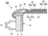
图1A表示基于本发明的安装有摄像元件芯片的基板的第一实施方式,是其剖视图。1A is a cross-sectional view showing a first embodiment of a substrate on which an imaging device chip is mounted according to the present invention.
图1B表示基于本发明的安装有摄像元件芯片的基板的第一实施方式,是其俯视图。FIG. 1B is a plan view showing a first embodiment of a substrate on which an imaging device chip is mounted according to the present invention.
图2是表示在图1A以及图1B的摄像元件芯片上设置有透镜以及棱镜的摄像模块的一个例子的剖视图。2 is a cross-sectional view showing an example of an imaging module in which a lens and a prism are provided on the imaging element chip of FIGS. 1A and 1B .
图3是从与透镜相对的一侧观察图2的摄像模块的主视图。FIG. 3 is a front view of the camera module of FIG. 2 viewed from a side opposite to the lens.
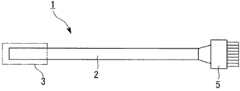
图4A是表示内窥镜的一个例子的俯视图。Fig. 4A is a plan view showing an example of an endoscope.
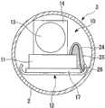
图4B是表示观测器前端部的一个例子的剖视图。Fig. 4B is a cross-sectional view showing an example of the front end of the scope.
图5是表示将图2的摄像模块插入观测器前端部的一个例子的主视图。Fig. 5 is a front view showing an example of inserting the camera module of Fig. 2 into the front end of the scope.
图6是表示用树脂密封图5的观测器前端部的一个例子的立体图。FIG. 6 is a perspective view showing an example of sealing the front end portion of the scope of FIG. 5 with resin.
图7A表示基于本发明的安装有摄像元件芯片的基板的第二实施方式,是其剖视图。FIG. 7A is a cross-sectional view showing a second embodiment of a substrate on which an imaging device chip is mounted according to the present invention.
图7B表示基于本发明的安装有摄像元件芯片的基板的第二实施方式,是其俯视图。7B is a plan view showing a second embodiment of the substrate on which the imaging element chip is mounted according to the present invention.
图8是表示在图7A以及图7B的摄像元件芯片上设置有透镜的摄像模块的一个例子的剖视图。8 is a cross-sectional view showing an example of an imaging module in which a lens is provided on the imaging element chip shown in FIGS. 7A and 7B .
具体实施方式Detailed ways
以下,基于优选的实施方式,参照附图对本发明进行说明。Hereinafter, the present invention will be described based on preferred embodiments with reference to the drawings.
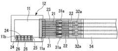
图1A以及图1B表示基于本发明的安装有摄像元件芯片11的基板12的第一实施方式。1A and 1B show a first embodiment of a
作为摄像元件芯片11,不特别进行限定,但举例有CMOS(Complementary Metal Oxide Semiconductor:互补型金属氧化膜半导体)、CCD(Charge coupled Device:电荷耦合器件)、CPD(Charge PrimingDevice:电荷引发器件)等半导体晶片。芯片尺寸不特别进行限定,但优选为了减小内窥镜所使用的管的直径而采用小型芯片,例如能够使用一边(长边以及短边)约为2mm以下、厚度约为0.5mm以下的芯片。The
如图4B以及图5所示,基板12使用柔性的基板,以便能够在内窥镜1的观测器前端部3中,在将基板12插入筒状的套管2内时,使基板12弯曲。As shown in FIGS. 4B and 5 , a flexible substrate is used for the
作为柔性的基板12,优选为在柔性的绝缘膜的单面或者双面形成有铜箔等金属层的柔性配线板(FPC)、和在柔性的绝缘膜的单面或者双面层叠有两层以上FPC的层叠配线板。作为绝缘膜,举例有聚酰亚胺、聚酯、液晶聚合物等,但不特别限定于此。基板12的厚度能够为例如50~200μm左右。As the
在第一实施方式的情况下,形成为经由粘合层33层叠多个以绝缘膜31b、32b为基材的FPC31、32,将通过FPC31、32的金属层的刻画图案而形成的连接部(第一基板连接部)31a、32a分隔为两层。由此,能够确保基板12的连接部(第一基板连接部)31a、32a的面积大于摄像元件芯片11的连接部(第一芯片连接部)11a的间距。在最上层的FPC32上层叠有包覆层34(保护膜),在包覆层34的绝缘膜34a的单面形成有粘合层34b。In the case of the first embodiment, a plurality of
在第一实施方式的摄像元件芯片11的安装方法中,首先,将摄像元件芯片11固定于基板12。将摄像元件芯片11固定于基板12的部件不特别进行限定,能够适当使用粘合剂、锡焊料、银焊料等接合材料17、螺钉等机械部件等。In the method of mounting the
在固定摄像元件芯片11后,将摄像元件芯片11的连接部(第一芯片连接部)11a、与基板12的连接部(第一基板连接部)31a、32a用导线(第一导线)21、22接线。另外,将摄像元件芯片11的连接部(第二芯片连接部)11b、与基板12的连接部(第二基板连接部)26用导线(第二导线)24接线。连接部11a、11b是形成于摄像元件芯片11的上表面的凸块等端子。另外,基板12的连接部31a、32a、26是形成于基板12的配线的焊盘等端子。作为导线21、22、24,例如举例有金(Au)线、铝(Al)线、铜(Cu)线等。After fixing the
在使用导线21、22、24来接线时,基板12也可以为根据内窥镜的摄像模块而任意决定的形状,例如平面状。因此,能够使用自动引线接合装置高效地进行作业。When connecting
在第一实施方式的情况下,摄像元件芯片11具有沿位于观测器前端部3的长度方向的一端(图1B的右侧)的短边排列的第一连接部(第一芯片连接部)11a、和沿位于与观测器前端部3的长度方向正交的一端(图1B的下侧)的长边排列的第二连接部(第二芯片连接部)11b。In the case of the first embodiment, the
基板12的连接部具有相对于摄像元件芯片11的第一连接部(第一芯片连接部)11a位于沿观测器前端部3的长度方向的方向(图1B中为左右方向)的第一连接部(第一基板连接部)31a、32a、和相对于摄像元件芯片11的第二连接部(第二芯片连接部)11b位于与观测器前端部3的长度方向正交的方向(图1B中为上下方向)的第二连接部(第二基板连接部)26。The connection portion of the
摄像元件芯片11的第一连接部(第一芯片连接部)11a与基板12的第一连接部(第一基板连接部)31a、32a之间,利用大致在沿观测器前端部3的长度方向的方向延伸的第一导线21、22进行接线。Between the first connection portion (first chip connection portion) 11a of the
另外,摄像元件芯片11的第二连接部(第二芯片连接部)11b与基板12的第二连接部(第二基板连接部)26之间,利用大致在与观测器前端部3的长度方向正交的方向延伸的第二导线24进行接线。In addition, between the second connection portion (second chip connection portion) 11b of the
由此,即使摄像元件芯片11具备多个连接部11a、11b,沿摄像元件芯片11的正交的两边设置有第一连接部11a以及第二连接部11b,也能够与基板12上的配线电连接而不出现各导线21、22、24混乱的情况。Thus, even if the
在将第一芯片连接部、与第一基板连接部用导线21、22接线后,用具有柔软性的非导电性的树脂23包覆导线21、22整体。另外,在将第二芯片连接部、与第二基板连接部用导线24接线后,用具有柔软性的非导电性的树脂25包覆导线24整体。由此,能够防止邻接的导线21、22、24彼此接触而防止电短路。另外,树脂23、25的包覆包括基板12的连接部31a、32a、26以及摄像元件芯片11的连接部11a、11b,由此还保护上述连接部与导线21、22、24之间的连接位置,从而提高耐久性。After connecting the first chip connection part and the first substrate connection part with
图2所示的第一实施方式的摄像模块10具备固定于摄像元件芯片11上的棱镜14、和安装于该棱镜14的物镜13作为用于使摄像元件芯片11的摄像区域成像光学图像的光学系统。棱镜14安装有支承部件15,并且利用粘合剂等棱镜14被固定于摄像元件芯片11中的摄像区域的周围16。The
物镜13可以为圆柱状的折射率分布型透镜(GRIN透镜),也可以为图8所示那样将透镜19安装于框架20的构造。The
此外,棱镜14、物镜13的安装,可以在将摄像元件芯片11安装于基板12后,也可以在这安装前。In addition, the mounting of the
根据第一实施方式的摄像元件芯片11的安装方法,基板12的连接部31a、32a与摄像元件芯片11的连接部11a之间,被具有挠性的导线21、22连接,并且被具有柔软性的非导电性的树脂23包覆,因此能够弯曲基板12。According to the mounting method of the
并且,基板12的连接部26与摄像元件芯片11的连接部11b之间,被具有挠性的导线24连接,并且被具有柔软性的非导电性的树脂25包覆,因此能够弯曲基板12。Furthermore, the
在为第一实施方式的摄像模块10的情况下,能够使基板12在基板12的第一连接部(第一基板连接部)31a、32a与摄像元件芯片11的第一连接部(第一芯片连接部)11a之间(第一基板连接部的附近,包括第一基板连接部与第一芯片连接部在内的区域)在长度方向弯曲(参照图8)。并且,能够使基板12在基板12的第二连接部(第二基板连接部)26与摄像元件芯片11的第二连接部(第二芯片连接部)11b之间(第二基板连接部的附近,包括第二基板连接部与第二芯片连接部在内的区域)在与长度方向正交的方向弯曲。In the case of the
具有柔软性的非导电性的树脂23、25优选为,显示出例如橡胶状、粘土状、凝胶状、果冻状、半固体状、糊状、浆状、液状等性状,具有可涂敷的程度的流动性的低粘度(例如1000~10000cP)。还能够在涂敷后进行固化、干燥等工序,在该情况下,只要固化、干燥后的树脂具有柔软性即可。The flexible
如图4B所示,图2所示的摄像模块10能够以在内窥镜1的观测器前端部3,插入套管2内的方式使用。柔性的基板12也可以在中途与导线、电缆等电信号线4连接。在图4A所示的内窥镜1中,在操作者所操作的一侧的端部设置连接器(电连接器)5,将电信号线4与连接器5内的端子(未图示)电连接。由此,能够将内窥镜1的电信号线4与视频处理器、个人计算机等图像显示装置一并连接。As shown in FIG. 4B , the
作为电信号线4,不特别进行限定,但优选极细同轴电缆(例如中心导体的尺寸按AWG(美国线规)在36以下的同轴电缆)。作为连接器5,不特别进行限定,但众所周知USB(通用串行总线:Universal SerialBus)等各种规格,都能够优选使用于本发明。The
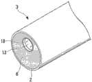
图5表示使摄像模块10的基板12在与观测器前端部3的长度方向正交的方向弯曲,并将其插入套管2内的状态。使基板12与接线于基板12的第二连接部26的导线24一起在与观测器前端部3的长度方向(图5中与纸面垂直)正交的方向弯曲并将其插入套管2。由此,与不使基板弯曲的情况相比能够减小基板12在与观测器前端部3的长度方向正交的方向的宽度,从而能够使用内径更小的套管2。此外,如图3所示,插入套管2前的摄像模块10也可以形成为基板12为平坦的。FIG. 5 shows a state in which the
在第一实施方式中,在摄像模块10上设置棱镜等光路变更部件,使摄像模块10的摄像区域朝向与观测器前端部3的长度方向正交的方向(图5中为上方),因此即使套管2的内径为略大于摄像元件芯片11的边的长度的大小,也能够插入摄像模块10。即,在本发明的第一实施方式中,能够使用内径小的套管。另一方面,如专利文献1(日本专利第3216650号公报)那样,在使摄像模块10的摄像区域朝向观测器前端部3的长度方向的情况下,为了收容摄像元件芯片11,需要套管2的内径大于摄像元件芯片11的对角线的长度(如图1B所示,从上部观察摄像元件芯片11时的摄像元件芯片11的对角线的长度)。In the first embodiment, an optical path changing member such as a prism is provided on the
图6表示在将摄像模块10插入套管2内后,用密封材料6密封套管2的前端部的状态。物镜13在观测器前端部3露出。还能够以为了防止密封材料6侵入物镜13的物面上,而在物镜13的周围使管18的端部突出,拦住密封材料6的方式构成。FIG. 6 shows a state where the front end portion of the
以上,根据优选的第一实施方式对本发明进行了说明,但本发明并不限定于上述的第一实施方式,在不脱离本发明的主旨的范围内能够进行各种改变。As mentioned above, although this invention was demonstrated based on preferable 1st Embodiment, this invention is not limited to said 1st Embodiment, Various changes are possible in the range which does not deviate from the summary of this invention.
图7A以及图7B表示本发明中安装有摄像元件芯片11的基板12的第二实施方式。7A and 7B show a second embodiment of the
在第二实施方式的情况下,基板12的连接部31a、32a相对于摄像元件芯片11的连接部11a位于沿观测器前端部3的长度方向的方向(图7B中为左右方向)。摄像元件芯片11的连接部11a与基板12的连接部31a、32a之间,利用在大致沿观测器前端部3的长度方向的方向延伸的导线21、22进行接线。In the case of the second embodiment, the connecting
第二实施方式的摄像元件芯片11的安装方法与第一实施方式相同,在将摄像元件芯片11固定于基板12,将基板12的连接部31a、32a与摄像元件芯片11的连接部11a用导线21、22接线后,用具有柔软性的非导电性的树脂23包覆导线21、22整体。The mounting method of the
由此,能够防止邻接的导线21、22彼此的接触而防止电短路。另外,树脂23的包覆包括基板12的连接部31a、32a以及摄像元件芯片11的连接部11a,由此还保护上述连接部与导线21、22之间的连接位置,提高耐久性。Accordingly, it is possible to prevent electrical short-circuiting by preventing adjacent
另外,基板12的连接部31a、32a与摄像元件芯片11的连接部11a之间(基板连接部的附近,包括基板连接部与芯片连接部在内的区域),被具有挠性的导线21、22连接,并且被具有柔软性的非导电性的树脂23包覆,因此能够弯曲基板12。In addition, between the
由此,与如专利文献1(日本专利第3216650号公报)的段落0040所记载那样以将连接基板折弯的状态连接导线框架的方法相比,在第二实施方式中,能够保持柔性的基板12平坦不变而进行具有挠性的导线21、22的接线,从而能够提高生产性。Thus, in the second embodiment, a flexible substrate can be maintained compared to the method of connecting the lead frame while the connection substrate is bent as described in paragraph 0040 of Patent Document 1 (Japanese Patent No. 3216650). 12 is flat, and the wiring of flexible
图8所示的第三实施方式的摄像模块10A作为用于使摄像元件芯片11的摄像区域成像光学图像的光学系统,将透镜19安装于框架20,从而固定于摄像元件芯片11上。The
第三实施方式的摄像模块10A能够使基板12在基板12的第一连接部31a、32a与摄像元件芯片11的连接部11a之间(基板连接部的附近,包括基板连接部与芯片连接部在内的区域)在长度方向弯曲,能够在内窥镜的观测器前端部将基板12插入套管(未图示)。In the
使用第四实施方式的摄像模块10A构成内窥镜的方法,能够与使用第一实施方式的摄像模块10的情况同样地实施。例如,如图6所示,还能够在将摄像模块插入套管内后,在物镜的周围用密封材料密封套管的前端部。The method of configuring an endoscope using the
根据第四实施方式的摄像模块10A,即使在将基板12的连接部31a、32a与摄像元件芯片11的连接部11a连接,并用树脂23包覆后也能够弯曲基板12,因此能够插入至直径更小的观测器前端部,从而能够以更简单的结构减小内窥镜的直径。According to the
附图标记说明:Explanation of reference signs:
1…内窥镜(观测器);2…套管;3…观测器前端部;10、10A…摄像模块;11…摄像元件芯片;11a…摄像元件芯片的第一连接部(第一芯片连接部);11b…摄像元件芯片的第二连接部(第二芯片连接部);12…基板;21、22…第一导线;24…第二导线;23、25…树脂;26…基板的第二连接部(第二基板连接部);31a、32a…基板的第一连接部(第一基板连接部)。1...endoscope (observer); 2...cannula; 3...the front end of the scope; 10, 10A...camera module; 11...camera chip; 11b...the second connection part of the imaging element chip (second chip connection part); 12...the substrate; 21, 22...the first lead; 24...the second lead; 23, 25...resin; Two connection parts (second board connection part); 31a, 32a... the first connection part of the board (first board connection part).
Claims (8)
Translated fromChineseApplications Claiming Priority (3)
| Application Number | Priority Date | Filing Date | Title |
|---|---|---|---|
| JP2011-249755 | 2011-11-15 | ||
| JP2011249755AJP5386567B2 (en) | 2011-11-15 | 2011-11-15 | Imaging device chip mounting method, endoscope assembling method, imaging module, and endoscope |
| PCT/JP2012/079522WO2013073578A1 (en) | 2011-11-15 | 2012-11-14 | Image capture element chip mounting method, endoscope assembly method, image capture module, and endoscope |
Publications (1)
| Publication Number | Publication Date |
|---|---|
| CN103889308Atrue CN103889308A (en) | 2014-06-25 |
Family
ID=48429633
Family Applications (1)
| Application Number | Title | Priority Date | Filing Date |
|---|---|---|---|
| CN201280053046.9APendingCN103889308A (en) | 2011-11-15 | 2012-11-14 | Image capture element chip mounting method, endoscope assembly method, image capture module, and endoscope |
Country Status (5)
| Country | Link |
|---|---|
| US (1) | US10510918B2 (en) |
| EP (1) | EP2781183B1 (en) |
| JP (1) | JP5386567B2 (en) |
| CN (1) | CN103889308A (en) |
| WO (1) | WO2013073578A1 (en) |
Cited By (4)
| Publication number | Priority date | Publication date | Assignee | Title |
|---|---|---|---|---|
| CN108010905A (en)* | 2016-10-27 | 2018-05-08 | 美国亚德诺半导体公司 | Compact integrated device encapsulation |
| CN109075567A (en)* | 2016-01-21 | 2018-12-21 | 力特有限公司 | Surface-mounted protective device |
| US11628275B2 (en) | 2018-01-31 | 2023-04-18 | Analog Devices, Inc. | Electronic devices |
| US11647678B2 (en) | 2016-08-23 | 2023-05-09 | Analog Devices International Unlimited Company | Compact integrated device packages |
Families Citing this family (18)
| Publication number | Priority date | Publication date | Assignee | Title |
|---|---|---|---|---|
| US20150229813A1 (en)* | 2013-02-11 | 2015-08-13 | Oran Jacob Isaac-Lowry | Miniature High Definition Camera System |
| US9257763B2 (en) | 2013-07-02 | 2016-02-09 | Gyrus Acmi, Inc. | Hybrid interconnect |
| US9510739B2 (en)* | 2013-07-12 | 2016-12-06 | Gyrus Acmi, Inc. | Endoscope small imaging system |
| WO2015050044A1 (en)* | 2013-10-04 | 2015-04-09 | オリンパスメディカルシステムズ株式会社 | Image pickup unit for endoscope |
| CN105830124B (en)* | 2013-10-15 | 2020-10-09 | 吉尔控股有限责任公司 | Micro HD Camera System |
| US9591758B2 (en) | 2014-03-27 | 2017-03-07 | Intel Corporation | Flexible electronic system with wire bonds |
| JP6431698B2 (en)* | 2014-06-16 | 2018-11-28 | オリンパス株式会社 | Imaging unit, wiring board with cable, and method of manufacturing wiring board with cable |
| JP6384879B2 (en) | 2015-01-23 | 2018-09-05 | オリンパス株式会社 | Imaging device and endoscope |
| KR102481003B1 (en)* | 2015-04-27 | 2022-12-26 | 엘지이노텍 주식회사 | Camera module |
| CN106358360B (en) | 2015-07-14 | 2019-07-19 | 财团法人工业技术研究院 | Flexible electronic device and manufacturing method thereof |
| JP6776840B2 (en)* | 2016-11-21 | 2020-10-28 | オムロン株式会社 | Electronic devices and their manufacturing methods |
| JP6695366B2 (en) | 2018-01-26 | 2020-05-20 | 株式会社フジクラ | Imaging module |
| WO2020097361A1 (en)* | 2018-11-07 | 2020-05-14 | Meditrina, Inc. | Endoscope and method of use |
| EP3930523A1 (en)* | 2019-02-26 | 2022-01-05 | Zeronoise Ltd | Apparatus to acquire and process images for a helmet, corresponding helmet and method to acquire and process images |
| WO2021149177A1 (en)* | 2020-01-22 | 2021-07-29 | オリンパス株式会社 | Imaging device, endoscope, and method for manufacturing imaging device |
| US11153970B1 (en) | 2020-07-20 | 2021-10-19 | Atl Technology, Llc | Apparatus with electrical components end mounted to printed circuit board |
| US11735879B2 (en) | 2021-03-09 | 2023-08-22 | Atl Technology, Llc | Adaptor for converting a ball grid array interface into a pin interface |
| US12177989B2 (en) | 2021-11-16 | 2024-12-24 | Atl Technology, Llc | Direct wire attachment methods and apparatus for a BGA component |
Citations (7)
| Publication number | Priority date | Publication date | Assignee | Title |
|---|---|---|---|---|
| US5220198A (en)* | 1990-08-27 | 1993-06-15 | Olympus Optical Co., Ltd. | Solid state imaging apparatus in which a solid state imaging device chip and substrate are face-bonded with each other |
| JP2005295050A (en)* | 2004-03-31 | 2005-10-20 | Miyota Kk | Camera module |
| US20080023784A1 (en)* | 2006-07-26 | 2008-01-31 | Olympus Corporation | Solid-state imaging apparatus |
| CN101672980A (en)* | 2008-09-08 | 2010-03-17 | 奥林巴斯医疗株式会社 | Imaging unit for endoscope |
| CN101808568A (en)* | 2007-09-28 | 2010-08-18 | 富士胶片株式会社 | Image pickup device and endoscope provided with image pickup device |
| US20110199473A1 (en)* | 2010-02-15 | 2011-08-18 | Olympus Corporation | Semiconductor apparatus and endoscope apparatus |
| JP2011212161A (en)* | 2010-03-31 | 2011-10-27 | Fujifilm Corp | Solid-state image pickup device and endoscopic device |
Family Cites Families (24)
| Publication number | Priority date | Publication date | Assignee | Title |
|---|---|---|---|---|
| JPS6077731A (en)* | 1983-10-03 | 1985-05-02 | オリンパス光学工業株式会社 | Endoscope apparatus using solid-image pick-up element |
| JPS6150544A (en) | 1984-08-20 | 1986-03-12 | オリンパス光学工業株式会社 | Endoscope |
| JPH0629911B2 (en) | 1985-05-07 | 1994-04-20 | 旭光学工業株式会社 | End tip structure of endoscope |
| US5418566A (en)* | 1990-09-10 | 1995-05-23 | Kabushiki Kaisha Toshiba | Compact imaging apparatus for electronic endoscope with improved optical characteristics |
| JPH0969983A (en)* | 1995-08-30 | 1997-03-11 | Matsushita Electric Ind Co Ltd | Solid-state imaging device |
| JP3623311B2 (en)* | 1996-05-17 | 2005-02-23 | オリンパス株式会社 | Solid-state imaging device |
| DE19924189C2 (en)* | 1999-05-27 | 2001-04-26 | Storz Karl Gmbh & Co Kg | Image sensor module and method for assembling such an image sensor module |
| JP2001051210A (en)* | 1999-08-05 | 2001-02-23 | Asahi Optical Co Ltd | Electronic endoscope |
| JP2001053988A (en)* | 1999-08-06 | 2001-02-23 | Asahi Optical Co Ltd | Flexible printed circuit board for wiring of electronic endoscope |
| JP4071580B2 (en)* | 2002-09-02 | 2008-04-02 | 株式会社フジクラ | Image fiber processing method |
| JP5030360B2 (en)* | 2002-12-25 | 2012-09-19 | オリンパス株式会社 | Method for manufacturing solid-state imaging device |
| US8118732B2 (en)* | 2003-04-01 | 2012-02-21 | Boston Scientific Scimed, Inc. | Force feedback control system for video endoscope |
| WO2005067783A1 (en)* | 2004-01-19 | 2005-07-28 | Olympus Corporation | Imaging device for endoscope and capsule type endoscope |
| DE602005021052D1 (en)* | 2004-01-19 | 2010-06-17 | Olympus Corp | MEDICAL TREATMENT DEVICE OF CAPSULE TYPE |
| JP4276678B2 (en)* | 2004-07-28 | 2009-06-10 | 富士通マイクロエレクトロニクス株式会社 | Imaging device |
| US8858425B2 (en)* | 2004-09-24 | 2014-10-14 | Vivid Medical, Inc. | Disposable endoscope and portable display |
| JP4812050B2 (en)* | 2004-12-17 | 2011-11-09 | 株式会社日立メディコ | Ultrasonic probe and ultrasonic diagnostic apparatus using the same |
| WO2007015426A1 (en)* | 2005-08-04 | 2007-02-08 | Nichia Corporation | Light-emitting device, method for manufacturing same, molded body and sealing member |
| JP2008109378A (en)* | 2006-10-25 | 2008-05-08 | Matsushita Electric Ind Co Ltd | Optical device module and manufacturing method thereof, and optical device unit and manufacturing method thereof |
| JP4682158B2 (en)* | 2007-01-16 | 2011-05-11 | オリンパスメディカルシステムズ株式会社 | Imaging device |
| JP4916595B2 (en)* | 2009-06-25 | 2012-04-11 | オリンパスメディカルシステムズ株式会社 | Imaging unit |
| US8698887B2 (en)* | 2010-04-07 | 2014-04-15 | Olympus Corporation | Image pickup apparatus, endoscope and manufacturing method for image pickup apparatus |
| JP5586402B2 (en)* | 2010-09-29 | 2014-09-10 | 富士フイルム株式会社 | Endoscope apparatus and imaging element heat dissipation method thereof |
| JP5436470B2 (en)* | 2011-01-31 | 2014-03-05 | 富士フイルム株式会社 | Imaging device and electronic endoscope provided with the same |
- 2011
- 2011-11-15JPJP2011249755Apatent/JP5386567B2/ennot_activeExpired - Fee Related
- 2012
- 2012-11-14WOPCT/JP2012/079522patent/WO2013073578A1/enactiveApplication Filing
- 2012-11-14CNCN201280053046.9Apatent/CN103889308A/enactivePending
- 2012-11-14EPEP12849196.6Apatent/EP2781183B1/ennot_activeNot-in-force
- 2014
- 2014-05-12USUS14/275,214patent/US10510918B2/enactiveActive
Patent Citations (7)
| Publication number | Priority date | Publication date | Assignee | Title |
|---|---|---|---|---|
| US5220198A (en)* | 1990-08-27 | 1993-06-15 | Olympus Optical Co., Ltd. | Solid state imaging apparatus in which a solid state imaging device chip and substrate are face-bonded with each other |
| JP2005295050A (en)* | 2004-03-31 | 2005-10-20 | Miyota Kk | Camera module |
| US20080023784A1 (en)* | 2006-07-26 | 2008-01-31 | Olympus Corporation | Solid-state imaging apparatus |
| CN101808568A (en)* | 2007-09-28 | 2010-08-18 | 富士胶片株式会社 | Image pickup device and endoscope provided with image pickup device |
| CN101672980A (en)* | 2008-09-08 | 2010-03-17 | 奥林巴斯医疗株式会社 | Imaging unit for endoscope |
| US20110199473A1 (en)* | 2010-02-15 | 2011-08-18 | Olympus Corporation | Semiconductor apparatus and endoscope apparatus |
| JP2011212161A (en)* | 2010-03-31 | 2011-10-27 | Fujifilm Corp | Solid-state image pickup device and endoscopic device |
Cited By (5)
| Publication number | Priority date | Publication date | Assignee | Title |
|---|---|---|---|---|
| CN109075567A (en)* | 2016-01-21 | 2018-12-21 | 力特有限公司 | Surface-mounted protective device |
| US11647678B2 (en) | 2016-08-23 | 2023-05-09 | Analog Devices International Unlimited Company | Compact integrated device packages |
| CN108010905A (en)* | 2016-10-27 | 2018-05-08 | 美国亚德诺半导体公司 | Compact integrated device encapsulation |
| CN108010905B (en)* | 2016-10-27 | 2021-09-03 | 美国亚德诺半导体公司 | Compact integrated device package |
| US11628275B2 (en) | 2018-01-31 | 2023-04-18 | Analog Devices, Inc. | Electronic devices |
Also Published As
| Publication number | Publication date |
|---|---|
| WO2013073578A1 (en) | 2013-05-23 |
| US10510918B2 (en) | 2019-12-17 |
| EP2781183A1 (en) | 2014-09-24 |
| JP2013103011A (en) | 2013-05-30 |
| EP2781183A4 (en) | 2015-08-12 |
| JP5386567B2 (en) | 2014-01-15 |
| US20140249368A1 (en) | 2014-09-04 |
| EP2781183B1 (en) | 2018-02-21 |
Similar Documents
| Publication | Publication Date | Title |
|---|---|---|
| JP5386567B2 (en) | Imaging device chip mounting method, endoscope assembling method, imaging module, and endoscope | |
| US5021888A (en) | Miniaturized solid state imaging device | |
| CN104769720B (en) | Imaging device, endoscope, semiconductor device, and manufacturing method of semiconductor device | |
| US10015375B2 (en) | Image pickup apparatus and endoscope including the same | |
| EP2944248A1 (en) | Method for manufacturing semiconductor device, semiconductor device, and endoscope | |
| US20150011891A1 (en) | Cable connection structure, ultrasonic probe, and ultrasonic endoscope system | |
| CN111355036B (en) | Cable assembly, cable holder, and method of manufacturing a cable assembly | |
| JP2010263020A (en) | Optical device module | |
| JP2011095333A (en) | Mounting structure | |
| JP2007243550A (en) | Electronic apparatus | |
| CN106455952B (en) | The manufacturing method of camera unit, the distributing board with cable and the distributing board with cable | |
| CN107534713A (en) | Camera device | |
| JP6081170B2 (en) | Imaging apparatus, endoscope, and manufacturing method of imaging apparatus | |
| CN109417081B (en) | Chip packaging structure, method and electronic equipment | |
| JP2011146259A (en) | Opto-electric composite cable with substrate | |
| US7638865B2 (en) | Sensor package | |
| WO2017010165A1 (en) | Image pickup module and endoscope | |
| US10321814B2 (en) | Image pickup apparatus and endoscope | |
| JP6188479B2 (en) | Board module | |
| JPH08172177A (en) | Solid-state image pickup module and endoscope apparatus | |
| KR100947967B1 (en) | Camera module and its manufacturing method | |
| KR20160073860A (en) | Flexible cable and method of manufacturing the same | |
| CN112311987A (en) | Display panel and display device | |
| US20190231180A1 (en) | Imaging module | |
| WO2020137384A1 (en) | Imaging module |
Legal Events
| Date | Code | Title | Description |
|---|---|---|---|
| C06 | Publication | ||
| PB01 | Publication | ||
| C10 | Entry into substantive examination | ||
| SE01 | Entry into force of request for substantive examination | ||
| C02 | Deemed withdrawal of patent application after publication (patent law 2001) | ||
| WD01 | Invention patent application deemed withdrawn after publication | Application publication date:20140625 |