CN103887177A - Finned active area manufacturing method - Google Patents
Finned active area manufacturing methodDownload PDFInfo
- Publication number
- CN103887177A CN103887177ACN201410118084.9ACN201410118084ACN103887177ACN 103887177 ACN103887177 ACN 103887177ACN 201410118084 ACN201410118084 ACN 201410118084ACN 103887177 ACN103887177 ACN 103887177A
- Authority
- CN
- China
- Prior art keywords
- active area
- fin formula
- preparation
- separator
- isolation layer
- Prior art date
- Legal status (The legal status is an assumption and is not a legal conclusion. Google has not performed a legal analysis and makes no representation as to the accuracy of the status listed.)
- Pending
Links
- 238000004519manufacturing processMethods0.000titleabstractdescription5
- 239000004065semiconductorSubstances0.000claimsabstractdescription45
- 238000000034methodMethods0.000claimsabstractdescription37
- 239000013078crystalSubstances0.000claimsabstractdescription31
- 239000000463materialSubstances0.000claimsabstractdescription29
- 239000000758substrateSubstances0.000claimsabstractdescription21
- 238000005530etchingMethods0.000claimsabstractdescription12
- 238000002360preparation methodMethods0.000claimsdescription13
- VYPSYNLAJGMNEJ-UHFFFAOYSA-NSilicium dioxideChemical groupO=[Si]=OVYPSYNLAJGMNEJ-UHFFFAOYSA-N0.000claimsdescription5
- 238000005229chemical vapour depositionMethods0.000claimsdescription4
- 238000005498polishingMethods0.000claimsdescription4
- 229910052732germaniumInorganic materials0.000claimsdescription3
- GNPVGFCGXDBREM-UHFFFAOYSA-Ngermanium atomChemical compound[Ge]GNPVGFCGXDBREM-UHFFFAOYSA-N0.000claimsdescription3
- 229910021421monocrystalline siliconInorganic materials0.000claimsdescription3
- 230000003647oxidationEffects0.000claimsdescription3
- 238000007254oxidation reactionMethods0.000claimsdescription3
- 238000001039wet etchingMethods0.000claimsdescription3
- 230000015572biosynthetic processEffects0.000claimsdescription2
- 239000000377silicon dioxideSubstances0.000claims1
- 238000002955isolationMethods0.000abstractdescription49
- 229920002120photoresistant polymerPolymers0.000description4
- 229910052814silicon oxideInorganic materials0.000description3
- 239000000126substanceSubstances0.000description3
- 238000001312dry etchingMethods0.000description2
- 238000000407epitaxyMethods0.000description2
- 230000010354integrationEffects0.000description2
- 238000000206photolithographyMethods0.000description2
- 229910052710siliconInorganic materials0.000description2
- 239000010703siliconSubstances0.000description2
- JBRZTFJDHDCESZ-UHFFFAOYSA-NAsGaChemical compound[As]#[Ga]JBRZTFJDHDCESZ-UHFFFAOYSA-N0.000description1
- 208000032750Device leakageDiseases0.000description1
- 229910001218Gallium arsenideInorganic materials0.000description1
- 229910000530Gallium indium arsenideInorganic materials0.000description1
- XUIMIQQOPSSXEZ-UHFFFAOYSA-NSiliconChemical compound[Si]XUIMIQQOPSSXEZ-UHFFFAOYSA-N0.000description1
- KXNLCSXBJCPWGL-UHFFFAOYSA-N[Ga].[As].[In]Chemical compound[Ga].[As].[In]KXNLCSXBJCPWGL-UHFFFAOYSA-N0.000description1
- 150000001875compoundsChemical class0.000description1
- 230000007547defectEffects0.000description1
- 238000000151depositionMethods0.000description1
- 238000010586diagramMethods0.000description1
- 238000005429filling processMethods0.000description1
- 239000012212insulatorSubstances0.000description1
- 238000012986modificationMethods0.000description1
- 230000004048modificationEffects0.000description1
- 238000000059patterningMethods0.000description1
Images


Classifications
- H—ELECTRICITY
- H10—SEMICONDUCTOR DEVICES; ELECTRIC SOLID-STATE DEVICES NOT OTHERWISE PROVIDED FOR
- H10D—INORGANIC ELECTRIC SEMICONDUCTOR DEVICES
- H10D62/00—Semiconductor bodies, or regions thereof, of devices having potential barriers
- H10D62/10—Shapes, relative sizes or dispositions of the regions of the semiconductor bodies; Shapes of the semiconductor bodies
- H10D62/17—Semiconductor regions connected to electrodes not carrying current to be rectified, amplified or switched, e.g. channel regions
- H10D62/213—Channel regions of field-effect devices
- H10D62/221—Channel regions of field-effect devices of FETs
- H10D62/235—Channel regions of field-effect devices of FETs of IGFETs
- H10D62/292—Non-planar channels of IGFETs
Landscapes
- Element Separation (AREA)
Abstract
Description
Translated fromChinese技术领域technical field
本发明涉及半导体制造工艺,特别涉及一种鳍式有源区的制备方法。The invention relates to a semiconductor manufacturing process, in particular to a method for preparing a fin-type active region.
背景技术Background technique
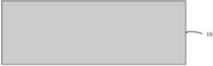
随着半导体器件特征尺寸按摩尔定律等比缩小,芯片集成度不断提高,出现的众多负面效应使传统的平面体硅MOS器件将因为短沟道效应和器件漏电、波动等问题,而很难再满足器件和电路的性能和功耗要求。近年来,一种新型器件结构Fin-typefield-effect transistors(FinFETs),其三维器件结构使得器件的短沟效应显著抑制,且具有更好的栅控能力,以及双栅的灵活控制等性能,越来越受到人们的关注。FinFET与平面型MOSFET结构的主要区别在于其沟道由衬底上凸起的高而薄的鳍(Fin)构成。如图1所示,衬底10上具有隔离层11和凸起的鳍状有源区121。有源区12包括突出于隔离层11顶面的上部和被隔离层11包围的下部。栅极结构13横跨在有源区12上,覆盖有源区12的上部的3个表面。有源区12上部被栅极结构覆盖的部分形成FinFET器件的沟道区,有源区12上部未被栅极结构覆盖的部分形成源漏。As the feature size of semiconductor devices shrinks proportionally according to Moore's law, and the integration level of chips continues to increase, many negative effects appear, making it difficult for traditional planar bulk silicon MOS devices to regenerate due to short-channel effects, device leakage, and fluctuations. Meet the performance and power requirements of devices and circuits. In recent years, a new type of device structure, Fin-typefield-effect transistors (FinFETs), whose three-dimensional device structure can significantly suppress the short-channel effect of the device, has better gate control capabilities, and flexible control of double gates. more and more people's attention. The main difference between a FinFET and a planar MOSFET structure is that its channel is formed by a tall and thin fin (Fin) raised from the substrate. As shown in FIG. 1 , the
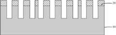
图2a至图2c所示为目前形成FinFET有源区的方法,其包括以下步骤:首先在衬底10上形成图形化的光刻胶层20,然后以图形化的光刻胶层20为掩膜在衬底10中刻蚀沟槽,去除光刻胶层后形成fin结构的有源区12。之后,在沟槽中形成隔离层11。该方法的缺点在于直接光刻刻蚀形成有源区的图形,很可能造成有源区顶部被圆化,且作为沟道的鳍式有源区侧壁容易受到刻蚀的等离子损伤。另一方面,形成隔离层的隔离工艺较为复杂,填充隔离层隔离介质时要保证不产生孔洞和其它类型的缺陷,工艺要求高,难度大,并也可能引入等离子损伤。Figure 2a to Figure 2c show the current method for forming the FinFET active region, which includes the following steps: firstly forming a patterned
有鉴于此,需要提供一种新的FinFET有源区的制备方法。In view of this, it is necessary to provide a new method for preparing the active region of the FinFET.
发明内容Contents of the invention
本发明的主要目的旨在提供一种鳍式有源区的制备方法,能够降低有源区损失、等离子体损伤和复杂工艺带来的高成本。The main purpose of the present invention is to provide a method for preparing a fin-type active region, which can reduce the loss of the active region, plasma damage and high cost caused by complicated processes.
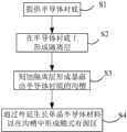
为达成上述目的,本发明提供一种鳍式有源区的制备方法,包括以下步骤:To achieve the above object, the present invention provides a method for preparing a fin-type active region, comprising the following steps:
S1,提供半导体衬底;S1, providing a semiconductor substrate;
S2,在所述半导体衬底上形成隔离层;S2, forming an isolation layer on the semiconductor substrate;
S3,刻蚀所述隔离层形成暴露所述半导体衬底的沟槽;以及S3, etching the isolation layer to form a trench exposing the semiconductor substrate; and
S4,通过外延生长单晶半导体材料以在所述沟槽中形成鳍式有源区,所述鳍式有源区具有突出于所述隔离层的顶面的部分。S4, growing a single crystal semiconductor material by epitaxy to form a fin-type active region in the trench, the fin-type active region having a portion protruding from a top surface of the isolation layer.
优选地,在所述沟槽中外延生长所述单晶半导体材料;进行平坦化以使所述单晶半导体材料的顶面与所述隔离层的上表面平齐;以及去除所述隔离层的上部部分以使所述鳍式有源区的顶面高于所述隔离层的顶面。Preferably, the single crystal semiconductor material is epitaxially grown in the trench; planarization is performed so that the top surface of the single crystal semiconductor material is flush with the upper surface of the isolation layer; and the isolation layer is removed. The upper part makes the top surface of the fin-type active region higher than the top surface of the isolation layer.
优选地,所述隔离层的材料为氧化硅。Preferably, the material of the isolation layer is silicon oxide.
优选地,所述隔离层的形成工艺为化学气相沉积或热氧化,其形成厚度为30nm~1000nm。Preferably, the formation process of the isolation layer is chemical vapor deposition or thermal oxidation, and the thickness of the isolation layer is 30nm-1000nm.
优选地,所述单晶半导体材料为单晶硅、锗单晶或III-V族单晶材料。Preferably, the single crystal semiconductor material is single crystal silicon, germanium single crystal or III-V single crystal material.
优选地,所述单晶半导体材料的平坦化工艺为刻蚀或化学机械抛光。Preferably, the planarization process of the single crystal semiconductor material is etching or chemical mechanical polishing.
优选地,去除所述隔离层的上部部分的工艺为湿法腐蚀或干法反刻工艺。Preferably, the process for removing the upper part of the isolation layer is a wet etching or dry etching process.
优选地,所述隔离层未去除部分的高度为20nm~900nm,所述鳍式有源区突出于所述隔离层顶面的部分的高度为10nm~500nm。Preferably, the height of the unremoved part of the isolation layer is 20nm-900nm, and the height of the part of the fin-type active region protruding from the top surface of the isolation layer is 10nm-500nm.
优选地,所述沟槽的宽度为5nm~50nm。Preferably, the width of the trench is 5nm˜50nm.
本发明所提出的鳍式有源区的制备方法,采用先形成隔离层并刻蚀隔离层形成沟槽,之后采用外延生长单晶半导体材料的方式形成鳍式有源区,可以避免现有技术中直接刻蚀形成鳍式有源区造成的等离子损伤,同时所形成的有源区顶部也不易圆化。此外,本发明还可简化工艺集成方案,无需采用高难度的隔离介质填充,易于实施,可有效降低工艺难度和成本。The preparation method of the fin-type active region proposed by the present invention adopts the method of first forming an isolation layer and etching the isolation layer to form a trench, and then adopts the method of epitaxially growing a single crystal semiconductor material to form a fin-type active region, which can avoid the existing technology. The plasma damage caused by direct etching to form the fin-type active region, and the top of the formed active region is not easy to round. In addition, the present invention can also simplify the process integration scheme, does not need to be filled with difficult isolation medium, is easy to implement, and can effectively reduce process difficulty and cost.
附图说明Description of drawings
图1为现有技术中FinFET器件的结构示意图;FIG. 1 is a schematic structural diagram of a FinFET device in the prior art;
图2a~2c为现有技术中FinFET器件有源区的制备方法的剖视图;2a-2c are cross-sectional views of the method for preparing the active region of the FinFET device in the prior art;
图3为本发明的鳍式有源区的制备方法的流程图;Fig. 3 is the flowchart of the preparation method of the fin type active region of the present invention;
图4a~4e为本发明一实施例的鳍式有源区的制备方法的剖视图。4a-4e are cross-sectional views of a method for manufacturing a fin-type active region according to an embodiment of the present invention.
具体实施方式Detailed ways
为使本发明的内容更加清楚易懂,以下结合说明书附图,对本发明的内容作进一步说明。当然本发明并不局限于该具体实施例,本领域内的技术人员所熟知的一般替换也涵盖在本发明的保护范围内。In order to make the content of the present invention clearer and easier to understand, the content of the present invention will be further described below in conjunction with the accompanying drawings. Of course, the present invention is not limited to this specific embodiment, and general replacements known to those skilled in the art are also covered within the protection scope of the present invention.
图3为本发明提供的鳍式有源区制备方法步骤流程图。FIG. 3 is a flow chart of steps in the method for preparing a fin-type active region provided by the present invention.
如图3所示,本具体实施方式提供的鳍式有源区制备方法,包括以下步骤:As shown in FIG. 3 , the fin-type active region preparation method provided in this specific embodiment includes the following steps:
步骤S1:提供半导体衬底。所述半导体衬底可以为形成有半导体器件的硅、形成有半导体器件的绝缘体上硅(SOI)、或者为形成有半导体器件的II-VI或者III-V族化合物半导体。Step S1: providing a semiconductor substrate. The semiconductor substrate may be silicon on which semiconductor devices are formed, silicon-on-insulator (SOI) on which semiconductor devices are formed, or II-VI or III-V compound semiconductors on which semiconductor devices are formed.
步骤S2:在半导体衬底上形成隔离层。Step S2: forming an isolation layer on the semiconductor substrate.
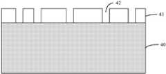
请参考图4a,该步骤中,隔离层一般为氧化硅层,在半导体衬底40上通过化学气相沉积或热氧化工艺形成氧化硅层41,其形成厚度科为30nm~1000nm。Please refer to FIG. 4a. In this step, the isolation layer is generally a silicon oxide layer, and the
步骤S3:刻蚀隔离层形成暴露半导体衬底的沟槽。Step S3: Etching the isolation layer to form a trench exposing the semiconductor substrate.
如图4b所示,在该步骤中,可采用包括光刻和蚀刻工艺的合适技术来制造沟槽。具体来说,包括在隔离层41上方沉积光刻胶层并图形化形成沟槽图形,根据该沟槽图形刻蚀隔离层41形成多个沟槽42。这些沟槽42的底部延伸至半导体衬底40,使衬底40暴露。这些沟槽42用于在后续步骤中形成鳍式有源区,而隔离层41中未刻蚀的部分则用于作为隔离区。一般的,沟槽的宽度为5nm~50nm。In this step, as shown in Figure 4b, trenches can be fabricated using suitable techniques including photolithography and etching processes. Specifically, it includes depositing a photoresist layer on the
步骤S4:通过外延生长单晶半导体材料以在沟槽中形成鳍式有源区。Step S4: growing a single crystal semiconductor material by epitaxy to form a fin-like active region in the trench.
首先请参考图4c,通过外延生长工艺在沟槽中生长单晶半导体材料43,使单晶半导体材料43填满沟槽。其中,单晶半导体材料可以为单晶硅,锗单晶,III-V族单晶材料如砷化镓单晶、铟镓砷单晶等,或其他单晶材料。First please refer to FIG. 4 c , a single
之后,进行平坦化工艺去除多余的单晶半导体材料43,形成如图4d所示的平面。具体的,将图4c所示的单晶半导体材料突出隔离层的部分去除直到隔离层的上表面露出,即单晶半导体材料的顶面与邻接的隔离层的上表面平齐。其中,多余单晶半导体材料的去除工艺可采用化学机械抛光或刻蚀工艺来进行。Afterwards, a planarization process is performed to remove excess single
接下来,去除隔离层41的上部部分,使得单晶半导体材料的顶面高于隔离层的顶面。隔离层上部部分的去除方法可采用湿法腐蚀或干法反刻工艺。如图4e所示,隔离层41未去除的部分形成FinFET器件的隔离区44,而单晶半导体材料45形成鳍式有源区,该鳍式有源区高于隔离层顶面的部分用于形成源漏区和沟道。因此,在去除隔离层上部部分后,可同时形成FinFET器件的鳍式有源区和隔离区。较佳的,隔离区44的高度为20nm~900nm,鳍式有源区突出于隔离层顶面的部分的高度为10nm~500nm。Next, the upper portion of the
综上所述,本发明所提供的鳍式有源区的制备方法,先形成具有有源区图形沟槽的隔离层,之后通过外延生长单晶半导体材料来形成鳍式有源区,避免了现有技术中直接在半导体衬底中刻蚀形成有源区造成有源区顶部圆化和等离子体损伤。另一方面本发明无需采用高难度的隔离层介质填充工艺,也省去了隔离层的化学机械抛光步骤,易于实施,更能够有效降低工艺难度和成本。To sum up, the preparation method of the fin-type active region provided by the present invention firstly forms the isolation layer with the pattern groove of the active region, and then forms the fin-type active region by epitaxially growing a single crystal semiconductor material, avoiding the In the prior art, the active region is formed directly by etching in the semiconductor substrate, resulting in rounding of the top of the active region and plasma damage. On the other hand, the present invention does not need to use a difficult dielectric filling process for the isolation layer, and also omits the step of chemical mechanical polishing of the isolation layer, which is easy to implement and can effectively reduce the difficulty and cost of the process.
虽然本发明已以较佳实施例揭示如上,然所述诸多实施例仅为了便于说明而举例而已,并非用以限定本发明,本领域的技术人员在不脱离本发明精神和范围的前提下可作若干的更动与润饰,本发明所主张的保护范围应以权利要求书所述为准。Although the present invention has been disclosed as above with preferred embodiments, the various embodiments described are only examples for convenience of description, and are not intended to limit the present invention. Those skilled in the art can Some changes and modifications are made, and the scope of protection claimed by the present invention should be based on the claims.
Claims (9)
Priority Applications (1)
| Application Number | Priority Date | Filing Date | Title |
|---|---|---|---|
| CN201410118084.9ACN103887177A (en) | 2014-03-27 | 2014-03-27 | Finned active area manufacturing method |
Applications Claiming Priority (1)
| Application Number | Priority Date | Filing Date | Title |
|---|---|---|---|
| CN201410118084.9ACN103887177A (en) | 2014-03-27 | 2014-03-27 | Finned active area manufacturing method |
Publications (1)
| Publication Number | Publication Date |
|---|---|
| CN103887177Atrue CN103887177A (en) | 2014-06-25 |
Family
ID=50956014
Family Applications (1)
| Application Number | Title | Priority Date | Filing Date |
|---|---|---|---|
| CN201410118084.9APendingCN103887177A (en) | 2014-03-27 | 2014-03-27 | Finned active area manufacturing method |
Country Status (1)
| Country | Link |
|---|---|
| CN (1) | CN103887177A (en) |
Cited By (3)
| Publication number | Priority date | Publication date | Assignee | Title |
|---|---|---|---|---|
| CN106558493A (en)* | 2015-09-29 | 2017-04-05 | 中芯国际集成电路制造(上海)有限公司 | The forming method of fin field effect pipe |
| CN107785419A (en)* | 2016-08-25 | 2018-03-09 | 中芯国际集成电路制造(上海)有限公司 | A kind of fin formula field effect transistor and its manufacture method |
| CN109994428A (en)* | 2017-12-29 | 2019-07-09 | 中芯国际集成电路制造(上海)有限公司 | Semiconductor structure and method of forming the same |
Citations (4)
| Publication number | Priority date | Publication date | Assignee | Title |
|---|---|---|---|---|
| US20050145926A1 (en)* | 2004-01-06 | 2005-07-07 | Lee Jong H. | Double-gate flash memory device and fabrication method thereof |
| US20050158970A1 (en)* | 2004-01-16 | 2005-07-21 | Robert Chau | Tri-gate transistors and methods to fabricate same |
| CN103177948A (en)* | 2011-12-22 | 2013-06-26 | 中芯国际集成电路制造(上海)有限公司 | Method for forming fin portion of fin field effect tube and fin field effect tube |
| CN103187286A (en)* | 2011-12-29 | 2013-07-03 | 中芯国际集成电路制造(上海)有限公司 | Manufacturing method of fin type field effect transistor |
- 2014
- 2014-03-27CNCN201410118084.9Apatent/CN103887177A/enactivePending
Patent Citations (4)
| Publication number | Priority date | Publication date | Assignee | Title |
|---|---|---|---|---|
| US20050145926A1 (en)* | 2004-01-06 | 2005-07-07 | Lee Jong H. | Double-gate flash memory device and fabrication method thereof |
| US20050158970A1 (en)* | 2004-01-16 | 2005-07-21 | Robert Chau | Tri-gate transistors and methods to fabricate same |
| CN103177948A (en)* | 2011-12-22 | 2013-06-26 | 中芯国际集成电路制造(上海)有限公司 | Method for forming fin portion of fin field effect tube and fin field effect tube |
| CN103187286A (en)* | 2011-12-29 | 2013-07-03 | 中芯国际集成电路制造(上海)有限公司 | Manufacturing method of fin type field effect transistor |
Cited By (6)
| Publication number | Priority date | Publication date | Assignee | Title |
|---|---|---|---|---|
| CN106558493A (en)* | 2015-09-29 | 2017-04-05 | 中芯国际集成电路制造(上海)有限公司 | The forming method of fin field effect pipe |
| CN106558493B (en)* | 2015-09-29 | 2020-10-09 | 中芯国际集成电路制造(上海)有限公司 | Method for forming fin field effect transistor |
| CN107785419A (en)* | 2016-08-25 | 2018-03-09 | 中芯国际集成电路制造(上海)有限公司 | A kind of fin formula field effect transistor and its manufacture method |
| CN107785419B (en)* | 2016-08-25 | 2020-09-01 | 中芯国际集成电路制造(上海)有限公司 | A kind of fin field effect transistor and its manufacturing method |
| CN109994428A (en)* | 2017-12-29 | 2019-07-09 | 中芯国际集成电路制造(上海)有限公司 | Semiconductor structure and method of forming the same |
| CN109994428B (en)* | 2017-12-29 | 2021-02-02 | 中芯国际集成电路制造(上海)有限公司 | Semiconductor structure and forming method thereof |
Similar Documents
| Publication | Publication Date | Title |
|---|---|---|
| CN103187439B (en) | Semiconductor structure and forming method thereof, CMOS and forming method thereof | |
| CN103811323B (en) | The preparation method of fin, fin formula field effect transistor and preparation method thereof | |
| CN102790004A (en) | Preparation method of full-isolation mixed crystal orientation crystal orientation silicon-on-insulator (SOI) | |
| CN105336597B (en) | A kind of preparation method of all-around-gate structure | |
| CN106486372A (en) | Semiconductor element and manufacturing method thereof | |
| CN103579001B (en) | Fin formula field effect transistor and forming method thereof | |
| CN105304490B (en) | Method of making a semiconductor structure | |
| CN103887177A (en) | Finned active area manufacturing method | |
| CN102651305B (en) | Preparation method of omega-shaped fin | |
| CN102790005B (en) | Method for selectively etching and preparing full-isolation mixed crystal orientation SOI (silicon-on-insulator) | |
| CN103258742B (en) | The formation method of transistor | |
| CN106571383B (en) | Semiconductor element and manufacturing method thereof | |
| CN104392917B (en) | A kind of forming method of all-around-gate structure | |
| CN105552126A (en) | Finned-type field effect transistor and fabrication method thereof | |
| CN105261587A (en) | Semiconductor device and method for manufacturing the same | |
| CN106252228B (en) | A method for forming a composite fin | |
| CN104103570B (en) | Method for enhancing isolation stress of shallow trench | |
| CN103632978A (en) | Formation method for semiconductor structure | |
| CN107516635A (en) | Fin field effect transistor and method of forming the same | |
| CN105280697A (en) | Semiconductor device and method for manufacturing the same | |
| CN104282565B (en) | Fin formula field effect transistor and forming method thereof | |
| CN111834299B (en) | Double fin structure and forming method thereof | |
| CN103794497B (en) | A kind of semiconductor device and its preparation method | |
| CN103165509B (en) | Preparation method of silicon-on-quasi-insulator field-effect transistor | |
| CN110034068A (en) | Semiconductor structure and forming method thereof |
Legal Events
| Date | Code | Title | Description |
|---|---|---|---|
| C06 | Publication | ||
| PB01 | Publication | ||
| C10 | Entry into substantive examination | ||
| SE01 | Entry into force of request for substantive examination | ||
| WD01 | Invention patent application deemed withdrawn after publication | Application publication date:20140625 | |
| WD01 | Invention patent application deemed withdrawn after publication |