CN103885660A - Embedded type touch screen and display device - Google Patents
Embedded type touch screen and display deviceDownload PDFInfo
- Publication number
- CN103885660A CN103885660ACN201410090141.7ACN201410090141ACN103885660ACN 103885660 ACN103885660 ACN 103885660ACN 201410090141 ACN201410090141 ACN 201410090141ACN 103885660 ACN103885660 ACN 103885660A
- Authority
- CN
- China
- Prior art keywords
- self
- capacitance
- touch screen
- touch
- electrodes
- Prior art date
- Legal status (The legal status is an assumption and is not a legal conclusion. Google has not performed a legal analysis and makes no representation as to the accuracy of the status listed.)
- Granted
Links
Images


Classifications
- G—PHYSICS
- G06—COMPUTING OR CALCULATING; COUNTING
- G06F—ELECTRIC DIGITAL DATA PROCESSING
- G06F3/00—Input arrangements for transferring data to be processed into a form capable of being handled by the computer; Output arrangements for transferring data from processing unit to output unit, e.g. interface arrangements
- G06F3/01—Input arrangements or combined input and output arrangements for interaction between user and computer
- G06F3/03—Arrangements for converting the position or the displacement of a member into a coded form
- G06F3/041—Digitisers, e.g. for touch screens or touch pads, characterised by the transducing means
- G06F3/0412—Digitisers structurally integrated in a display
- G—PHYSICS
- G06—COMPUTING OR CALCULATING; COUNTING
- G06F—ELECTRIC DIGITAL DATA PROCESSING
- G06F3/00—Input arrangements for transferring data to be processed into a form capable of being handled by the computer; Output arrangements for transferring data from processing unit to output unit, e.g. interface arrangements
- G06F3/01—Input arrangements or combined input and output arrangements for interaction between user and computer
- G06F3/03—Arrangements for converting the position or the displacement of a member into a coded form
- G06F3/041—Digitisers, e.g. for touch screens or touch pads, characterised by the transducing means
- G06F3/0416—Control or interface arrangements specially adapted for digitisers
- G06F3/04164—Connections between sensors and controllers, e.g. routing lines between electrodes and connection pads
- G—PHYSICS
- G06—COMPUTING OR CALCULATING; COUNTING
- G06F—ELECTRIC DIGITAL DATA PROCESSING
- G06F3/00—Input arrangements for transferring data to be processed into a form capable of being handled by the computer; Output arrangements for transferring data from processing unit to output unit, e.g. interface arrangements
- G06F3/01—Input arrangements or combined input and output arrangements for interaction between user and computer
- G06F3/03—Arrangements for converting the position or the displacement of a member into a coded form
- G06F3/041—Digitisers, e.g. for touch screens or touch pads, characterised by the transducing means
- G06F3/044—Digitisers, e.g. for touch screens or touch pads, characterised by the transducing means by capacitive means
- G06F3/0443—Digitisers, e.g. for touch screens or touch pads, characterised by the transducing means by capacitive means using a single layer of sensing electrodes
- G—PHYSICS
- G06—COMPUTING OR CALCULATING; COUNTING
- G06F—ELECTRIC DIGITAL DATA PROCESSING
- G06F3/00—Input arrangements for transferring data to be processed into a form capable of being handled by the computer; Output arrangements for transferring data from processing unit to output unit, e.g. interface arrangements
- G06F3/01—Input arrangements or combined input and output arrangements for interaction between user and computer
- G06F3/03—Arrangements for converting the position or the displacement of a member into a coded form
- G06F3/041—Digitisers, e.g. for touch screens or touch pads, characterised by the transducing means
- G06F3/0416—Control or interface arrangements specially adapted for digitisers
- G06F3/04166—Details of scanning methods, e.g. sampling time, grouping of sub areas or time sharing with display driving
Landscapes
- Engineering & Computer Science (AREA)
- General Engineering & Computer Science (AREA)
- Theoretical Computer Science (AREA)
- Human Computer Interaction (AREA)
- Physics & Mathematics (AREA)
- General Physics & Mathematics (AREA)
- Computer Networks & Wireless Communication (AREA)
- Position Input By Displaying (AREA)
Abstract
Translated fromChineseDescription
Translated fromChinese技术领域technical field
本发明涉及触控技术领域,尤其涉及一种内嵌式触摸屏及显示装置。The invention relates to the field of touch technology, in particular to an embedded touch screen and a display device.
背景技术Background technique
随着显示技术的飞速发展,触摸屏(Touch Screen Panel)已经逐渐遍及人们的生活中。目前,触摸屏按照组成结构可以分为:外挂式触摸屏(Add on ModeTouch Panel)、覆盖表面式触摸屏(On Cell Touch Panel)、以及内嵌式触摸屏(InCell Touch Panel)。其中,外挂式触摸屏是将触摸屏与液晶显示屏(Liquid CrystalDisplay,LCD)分开生产,然后贴合到一起成为具有触摸功能的液晶显示屏,外挂式触摸屏存在制作成本较高、光透过率较低、模组较厚等缺点。而内嵌式触摸屏将触摸屏的触控电极内嵌在液晶显示屏内部,可以减薄模组整体的厚度,又可以大大降低触摸屏的制作成本,受到各大面板厂家青睐。With the rapid development of display technology, touch screen (Touch Screen Panel) has gradually spread in people's life. At present, touch screens can be divided into three types according to their composition: Add on Mode Touch Panel, On Cell Touch Panel, and InCell Touch Panel. Among them, the plug-in touch screen is produced separately from the touch screen and Liquid Crystal Display (LCD), and then bonded together to form a touch-enabled LCD screen. The plug-in touch screen has high production costs and low light transmittance. , The module is thicker and other shortcomings. The embedded touch screen embeds the touch electrodes of the touch screen inside the liquid crystal display, which can reduce the overall thickness of the module and greatly reduce the production cost of the touch screen, and is favored by major panel manufacturers.
目前,现有的电容式内嵌(In cell)触摸屏是在现有的TFT(Thin FilmTransistor,薄膜场效应晶体管)阵列基板上直接另外增加触控驱动电极和触控感应电极实现的,即在TFT阵列基板的表面制作两层相互异面相交的条状ITO电极,这两层ITO(Indium Tin Oxides,铟锡金属氧化物)电极分别作为触摸屏的触控驱动电极和触控感应电极,如图1所示,横向设置的触控驱动电极Tx和纵向设置的触控感应电极Rx之间耦合产生互电容Cm(MutualCapacitance),当手指触碰屏幕时,手指的触碰会改变互电容Cm的值,触摸检测装置通过检测手指触碰前后电容Cm对应的电流的改变量,从而检测出手指触摸点的位置。At present, the existing capacitive in-cell (In cell) touch screen is realized by adding touch driving electrodes and touch sensing electrodes directly on the existing TFT (Thin Film Transistor, thin film field effect transistor) array substrate, that is, in the TFT On the surface of the array substrate, two layers of strip-shaped ITO electrodes that intersect with each other in different planes are made. These two layers of ITO (Indium Tin Oxides, indium tin metal oxide) electrodes are respectively used as touch driving electrodes and touch sensing electrodes of the touch screen, as shown in Figure 1 As shown, the coupling between the horizontally arranged touch drive electrodes Tx and the vertically arranged touch sensing electrodes Rx generates a mutual capacitance Cm (MutualCapacitance). When a finger touches the screen, the touch of the finger will change the value of the mutual capacitance Cm The touch detection device detects the position of the finger touch point by detecting the change amount of the current corresponding to the capacitance Cm before and after the finger touch.
在横向设置的触控驱动电极Tx和纵向设置的触控感应电极Rx之间会形成两种互电容Cm,如图1所示,一种是对实现触摸功能有效的投射电容(图1中带箭头的曲线为投射电容),手指触碰屏幕时,会改变投射电容值;另一种是对实现触摸功能无效的正对电容(带箭头的直线为正对电容),手指触碰屏幕时,正对电容值不会发生变化。Two kinds of mutual capacitance Cm will be formed between the touch driving electrodes Tx arranged horizontally and the touch sensing electrodes Rx arranged vertically, as shown in Figure 1, one is the projected capacitance that is effective for realizing the touch function (in Figure 1 The curve with the arrow is the projected capacitance), when the finger touches the screen, it will change the projected capacitance value; the other is the positive capacitance that is ineffective for realizing the touch function (the straight line with the arrow is the positive capacitance), when the finger touches the screen , the positive value of the capacitance does not change.
上述电容式内嵌触摸屏的结构设计中,在人体电容仅会与互电容中的投射电容发生耦合作用,触控驱动电极与触控感应电极在正对面处形成的正对电容会使触摸屏的信噪比降低,影响了内嵌式触摸屏中触控感应的准确性。并且,需要在现有的TFT阵列基板上增加两层新的膜层,导致在制作TFT阵列基板时需要增加新的工艺,使生产成本增加,不利于提高生产效率。In the structural design of the above-mentioned capacitive embedded touch screen, the human body capacitance will only couple with the projected capacitance in the mutual capacitance, and the facing capacitance formed by the touch driving electrode and the touch sensing electrode on the opposite side will make the signal of the touch screen The noise ratio is reduced, which affects the accuracy of touch sensing in the embedded touch screen. Moreover, it is necessary to add two new film layers on the existing TFT array substrate, resulting in the need to add a new process when manufacturing the TFT array substrate, which increases the production cost and is not conducive to improving production efficiency.
发明内容Contents of the invention
有鉴于此,本发明实施例提供了一种内嵌式触摸屏及显示装置,用以实现触控精度较高、成本较低、生产效率较高且透过率较高的内嵌式触摸屏。In view of this, an embodiment of the present invention provides an in-cell touch screen and a display device for realizing an in-cell touch screen with high touch accuracy, low cost, high production efficiency and high transmittance.
因此,本发明实施例提供的一种内嵌式触摸屏,包括相对设置的上基板和下基板,所述上基板面向所述下基板的一侧具有平坦层以及位于平坦层之上隔垫物层,还包括:Therefore, an in-cell touch screen provided by an embodiment of the present invention includes an upper substrate and a lower substrate oppositely arranged, and the side of the upper substrate facing the lower substrate has a flat layer and a spacer layer on the flat layer. ,Also includes:
设置于所述平坦层和所述隔垫物层之间的多个同层设置且相互绝缘的自电容电极,以及在触控时间段通过检测各所述自电容电极的电容值变化以判断触控位置的触控侦测芯片。A plurality of self-capacitance electrodes arranged on the same layer and insulated from each other are arranged between the flat layer and the spacer layer, and during the touch time period, the capacitance value change of each of the self-capacitance electrodes is detected to determine the touch The touch detection chip of the control position.
本发明实施例提供的上述内嵌式触摸屏,利用自电容的原理在触摸屏的上基板设置多个同层设置且相互绝缘的自电容电极,当人体未触碰屏幕时,各自电容电极所承受的电容为一固定值,当人体触碰屏幕时,对应的自电容电极所承受的电容为固定值叠加人体电容,触控侦测芯片在触控时间段通过检测各自电容电极的电容值变化可以判断出触控位置。由于人体电容可以作用于全部自电容,相对于人体电容仅能作用于互电容中的投射电容,由人体碰触屏幕所引起的触控变化量会比较大,因此能有效提高触控的信噪比,从而提高触控感应的准确性。并且,相对于采用互电容原理实现触控功能时需要在现有的阵列基板内增加两层新的膜层,本发明实施例提供的触摸屏中仅需要增加一层自电容电极即可实现触控功能,节省了生产成本,提高了生产效率。The above-mentioned embedded touch screen provided by the embodiment of the present invention uses the principle of self-capacitance to set a plurality of self-capacitance electrodes on the same layer and insulated from each other on the upper substrate of the touch screen. When the human body does not touch the screen, the respective capacitance electrodes bear The capacitance is a fixed value. When the human body touches the screen, the capacitance of the corresponding self-capacitance electrode is a fixed value superimposed on the capacitance of the human body. The touch detection chip can judge by detecting the change of the capacitance value of each capacitance electrode during the touch time period. out of the touch position. Since human body capacitance can act on all self-capacitance, compared with human body capacitance, which can only act on projected capacitance in mutual capacitance, the amount of touch changes caused by human body touching the screen will be relatively large, so it can effectively improve the signal-to-noise of touch Ratio, thereby improving the accuracy of touch sensing. Moreover, compared to the need to add two new film layers in the existing array substrate when the mutual capacitance principle is used to realize the touch function, the touch screen provided by the embodiment of the present invention only needs to add a layer of self-capacitance electrodes to realize touch control. Function, saving production cost and improving production efficiency.
进一步地,相对于自电容电极设置在上基板与平坦层之间时需要对平坦层进行构图露出与自电容电极的同层设置的导通连接点,该导通连接点通过边框胶与位于下基板的触控侦测芯片的连接端子电性连接,本发明实施例提供的触摸屏中由于自电容电极设置在上基板的平坦层与隔垫物层之间,因此,可以省去对平坦层进行构图,与自电容电极的同层设置的导通连接点即可直接通过边框胶与位于下基板的触控侦测芯片的连接端子电性连接,节省了制作工艺。Further, when the self-capacitance electrode is arranged between the upper substrate and the flat layer, it is necessary to pattern the flat layer to expose the conduction connection point provided on the same layer as the self-capacitance electrode. The connection terminals of the touch detection chip on the substrate are electrically connected. In the touch screen provided by the embodiment of the present invention, since the self-capacitance electrode is arranged between the flat layer of the upper substrate and the spacer layer, the flat layer can be omitted. Composition, the conduction connection point provided on the same layer as the self-capacitance electrode can be directly electrically connected to the connection terminal of the touch detection chip located on the lower substrate through the frame glue, which saves the manufacturing process.
在一种可能的实现方式中,在本发明实施例提供的上述内嵌式触摸屏中,还包括:设置于所述上基板和所述下基板之间的黑矩阵层;In a possible implementation manner, the above-mentioned in-cell touch screen provided by the embodiment of the present invention further includes: a black matrix layer arranged between the upper substrate and the lower substrate;
各所述自电容电极的图形在所述下基板上的正投影位于所述黑矩阵层的图形所在区域内。The orthographic projection of the pattern of each self-capacitance electrode on the lower substrate is located in the area where the pattern of the black matrix layer is located.
在一种可能的实现方式中,在本发明实施例提供的上述内嵌式触摸屏中,各所述自电容电极的图形为在所述下基板上的正投影位于所述黑矩阵层的图形所在区域内的网格状结构。In a possible implementation manner, in the above-mentioned in-cell touch screen provided by the embodiment of the present invention, the pattern of each self-capacitance electrode is where the orthographic projection on the lower substrate is located on the pattern of the black matrix layer. Grid-like structure in the area.
在一种可能的实现方式中,本发明实施例提供的上述内嵌式触摸屏,还包括:与各所述自电容电极一一对应的导线,以及与所述自电容电极一一对应的导通连接点;其中,In a possible implementation manner, the above-mentioned in-cell touch screen provided by the embodiment of the present invention further includes: wires corresponding to the self-capacitance electrodes one-to-one, and conducting wires corresponding to the self-capacitance electrodes one-to-one connection point; where,
各所述导线在所述下基板上的正投影位于所述黑矩阵层的图形所在区域内,各所述导通连接点设置在所述内嵌式触摸屏的边框胶所在区域;The orthographic projection of each of the wires on the lower substrate is located in the area where the pattern of the black matrix layer is located, and each of the conductive connection points is arranged in the area where the frame glue of the embedded touch screen is located;
各所述自电容电极通过所述导线连接至所述导通连接点后,通过位于所述边框胶所在区域的走线与所述触控侦测芯片的连接端子电性连接。After each self-capacitance electrode is connected to the conductive connection point through the wire, it is electrically connected to the connection terminal of the touch detection chip through the wiring located in the area where the frame glue is located.
在一种可能的实现方式中,在本发明实施例提供的上述内嵌式触摸屏中,各所述导线与各所述自电容电极同层设置。In a possible implementation manner, in the above-mentioned in-cell touch screen provided by the embodiment of the present invention, each of the wires and each of the self-capacitance electrodes are arranged on the same layer.
在一种可能的实现方式中,在本发明实施例提供的上述内嵌式触摸屏中,所述内嵌式触摸屏的边框胶所在区域具有四个侧边,所述导通连接点在所述边框胶所在区域的四个侧边均有分布。In a possible implementation manner, in the above-mentioned in-cell touch screen provided by the embodiment of the present invention, the area where the frame glue of the in-cell touch screen is located has four sides, and the conductive connection point is located on the frame There are distributions on the four sides of the area where the glue is located.
在一种可能的实现方式中,在本发明实施例提供的上述内嵌式触摸屏中,与各所述自电容电极对应的导通连接点分布在离所述自电容电极距离最近的边框胶所在区域的侧边处。In a possible implementation manner, in the above-mentioned in-cell touch screen provided by the embodiment of the present invention, the conduction connection points corresponding to the self-capacitance electrodes are distributed at the border glue closest to the self-capacitance electrodes side of the area.
在一种可能的实现方式中,在本发明实施例提供的上述内嵌式触摸屏中,所述导线与所述自电容电极异层设置,所述导线设置于所述上基板与所述平坦层之间,所述自电容电极与对应的导线通过过孔电性连接。In a possible implementation manner, in the above-mentioned in-cell touch screen provided by the embodiment of the present invention, the wire and the self-capacitance electrode are arranged in different layers, and the wire is arranged on the upper substrate and the flat layer Between, the self-capacitance electrodes are electrically connected with the corresponding wires through via holes.
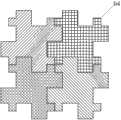
在一种可能的实现方式中,在本发明实施例提供的上述内嵌式触摸屏中,相邻的两个所述自电容电极相对的侧边均为折线。In a possible implementation manner, in the above-mentioned in-cell touch screen provided by the embodiment of the present invention, the opposite sides of two adjacent self-capacitance electrodes are fold lines.
在一种可能的实现方式中,在本发明实施例提供的上述内嵌式触摸屏中,相邻的两个自电容电极相对的为折线的侧边均具有阶梯状结构,两阶梯状结构形状一致且相互匹配;和/或,In a possible implementation, in the above-mentioned in-cell touch screen provided by the embodiment of the present invention, the sides opposite to the broken lines of two adjacent self-capacitance electrodes all have a stepped structure, and the two stepped structures have the same shape and match each other; and/or,
相邻的两个自电容电极相对的为折线的侧边均具有凹凸状结构,两凹凸状结构形状一致且相互匹配。The sides opposite to the broken lines of two adjacent self-capacitance electrodes have concave-convex structures, and the shapes of the two concave-convex structures are consistent and matched with each other.
本发明实施例提供的一种显示装置,包括本发明实施例提供的上述内嵌式触摸屏。A display device provided by an embodiment of the present invention includes the above-mentioned in-cell touch screen provided by the embodiment of the present invention.
附图说明Description of drawings
图1为现有的触控驱动电极和触控感应电极之间产生的电容示意图;FIG. 1 is a schematic diagram of capacitance generated between conventional touch driving electrodes and touch sensing electrodes;
图2为本发明实施例提供的内嵌式触摸屏的结构示意图;FIG. 2 is a schematic structural diagram of an embedded touch screen provided by an embodiment of the present invention;
图3为本发明实施例提供的内嵌式触摸屏的驱动时序示意图;FIG. 3 is a schematic diagram of a driving sequence of an embedded touch screen provided by an embodiment of the present invention;
图4为本发明实施例提供的内嵌式触摸屏中一个自电容电极的结构示意图;4 is a schematic structural diagram of a self-capacitance electrode in an in-cell touch screen provided by an embodiment of the present invention;
图5a为本发明实施例提供的内嵌式触摸屏中采用传统走线方式同层设置的导线和自电容电极的示意图;Fig. 5a is a schematic diagram of wires and self-capacitance electrodes arranged on the same layer using a traditional wiring method in an in-cell touch screen provided by an embodiment of the present invention;
图5b为本发明实施例提供的内嵌式触摸屏中导线和自电容电极同层设置的示意图;Fig. 5b is a schematic diagram of setting wires and self-capacitance electrodes on the same layer in the in-cell touch screen provided by the embodiment of the present invention;
图6为本发明实施例提供的内嵌式触摸屏中显示区域的自电容电极分区示意图;6 is a schematic diagram of self-capacitance electrode partitions in the display area of the in-cell touch screen provided by the embodiment of the present invention;
图7为本发明实施例提供的内嵌式触摸屏中各区域内同层设置的自电容电极与导通连接点的连接示意图;7 is a schematic diagram of the connection between the self-capacitance electrodes and the conduction connection points arranged on the same layer in each area of the in-cell touch screen provided by the embodiment of the present invention;
图8为本发明实施例提供的内嵌式触摸屏中自电容电极与导线的异层设置的示意图;FIG. 8 is a schematic diagram of different layers of self-capacitance electrodes and wires in an in-cell touch screen provided by an embodiment of the present invention;
图9为本发明实施例提供的内嵌式触摸屏中各区域异层层设置的自电容电极与导通连接点的连接示意图;9 is a schematic diagram of the connection between the self-capacitance electrodes and the conductive connection points arranged in different layers in each area of the in-cell touch screen provided by the embodiment of the present invention;
图10a和图10b分别为本发明实施例提供的内嵌式触摸屏中相邻的自电容电极相对的侧边设置为折线的结构示意图。Fig. 10a and Fig. 10b are schematic structural diagrams in which opposite sides of adjacent self-capacitance electrodes in the in-cell touch screen provided by an embodiment of the present invention are arranged as broken lines.
具体实施方式Detailed ways
下面结合附图,对本发明实施例提供的内嵌式触摸屏及显示装置的具体实施方式进行详细地说明。The specific implementation manners of the in-cell touch screen and the display device provided by the embodiments of the present invention will be described in detail below with reference to the accompanying drawings.
附图中各层膜层的厚度和形状不反映真实比例,目的只是示意说明本发明内容。The thickness and shape of each film layer in the drawings do not reflect the real scale, and the purpose is only to illustrate the content of the present invention.
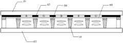
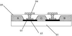
本发明实施例提供的一种内嵌式触摸屏,如图2所示,包括相对设置的上基板01和下基板02,上基板01面向下基板02的一侧具有平坦层09以及位于平坦层之上隔垫物层10,还包括:An in-cell touch screen provided by an embodiment of the present invention, as shown in FIG. 2 , includes an
设置于平坦层09和隔垫物层10之间的多个同层设置且相互绝缘的自电容电极04,以及在触控时间段通过检测各自电容电极的电容值变化以判断触控位置的触控侦测芯片。A plurality of self-
本发明实施例提供的上述内嵌式触摸屏,利用自电容的原理在触摸屏的上基板01设置多个同层设置且相互绝缘的自电容电极04,当人体未触碰屏幕时,各自电容电极04所承受的电容为一固定值,当人体触碰屏幕时,对应的自电容电极04所承受的电容为固定值叠加人体电容,触控侦测芯片在触控时间段通过检测各自电容电极04的电容值变化可以判断出触控位置。由于人体电容可以作用于全部自电容,相对于人体电容仅能作用于互电容中的投射电容,由人体碰触屏幕所引起的触控变化量会比较大,因此能有效提高触控的信噪比,从而提高触控感应的准确性。The above-mentioned embedded touch screen provided by the embodiment of the present invention uses the principle of self-capacitance to set a plurality of self-
进一步地,相对于自电容电极设置在上基板与平坦层之间时需要对平坦层进行构图露出与自电容电极的同层设置的导通连接点,该导通连接点通过边框胶与位于下基板的触控侦测芯片的连接端子电性连接,本发明实施例提供的触摸屏中由于自电容电极设置在上基板的平坦层与隔垫物层之间,因此,可以省去对平坦层进行构图,与自电容电极的同层设置的导通连接点即可直接通过边框胶与位于下基板的触控侦测芯片的连接端子电性连接,节省了制作工艺。Further, when the self-capacitance electrode is arranged between the upper substrate and the flat layer, it is necessary to pattern the flat layer to expose the conduction connection point provided on the same layer as the self-capacitance electrode. The connection terminals of the touch detection chip on the substrate are electrically connected. In the touch screen provided by the embodiment of the present invention, since the self-capacitance electrode is arranged between the flat layer of the upper substrate and the spacer layer, the flat layer can be omitted. Composition, the conduction connection point provided on the same layer as the self-capacitance electrode can be directly electrically connected to the connection terminal of the touch detection chip located on the lower substrate through the frame glue, which saves the manufacturing process.
在具体实施时,为了能有效检测出各自电容电极04的电容值变化,触控侦测芯片可以在触控时间段向各自电容电极04施加驱动信号,并接受各自电容电极04的反馈信号,由自电容电极04被触摸引起的电容值变化会增加反馈信号的RC延时,通过判断各自电容电极04的反馈信号RC延时即可确定自电容电极04是否被触摸,从而定位触控位置,当然,触控侦测芯片还可以通过诸如检测电荷变化量的其他方式确认各自电容电极04的电容值变化以判断触控位置,在此不做赘述。During specific implementation, in order to effectively detect changes in the capacitance values of the respective
进一步地,为了降低显示信号和触控信号之间的相互干扰,提高画面品质和触控准确性,在本发明实施例提供的上述触摸屏中,触控和显示阶段还可以采用分时驱动的方式,并且,在具体实施时还可以将显示驱动芯片和触控侦测芯片整合为一个芯片,进一步降低生产成本。Furthermore, in order to reduce the mutual interference between the display signal and the touch signal, and improve the image quality and touch accuracy, in the above touch screen provided by the embodiment of the present invention, the touch and display stages can also be driven in a time-sharing manner. , and, in actual implementation, the display driver chip and the touch detection chip can also be integrated into one chip, further reducing the production cost.
具体地,例如:如图3所示的驱动时序图中,将触摸屏显示每一帧(V-sync)的时间分成显示时间段(Display)和触控时间段(Touch),例如图3所示的驱动时序图中触摸屏的显示一帧的时间为16.7ms,选取其中5ms作为触控时间段,其他的11.7ms作为显示时间段,当然也可以根据IC芯片的处理能力适当的调整两者的时长,在此不做具体限定。在显示时间段(Display),对触摸屏中的每条栅极信号线Gate1,Gate2……Gate n依次施加栅扫描信号,对数据信号线Data施加灰阶信号,实现液晶显示功能。在触控时间段(Touch),与各自电容电极Cx1……Cx n连接的触控侦测芯片向各触控驱动电极Cx1……Cx n分别施加驱动信号,同时接收各自电容电极Cx1……Cx n的反馈信号,通过对反馈信号的分析判断是否发生触控,以实现触控功能。Specifically, for example: in the driving timing diagram shown in Figure 3, the time for the touch screen to display each frame (V-sync) is divided into a display period (Display) and a touch period (Touch), as shown in Figure 3 The display time of one frame of the touch screen in the driving sequence diagram is 16.7ms, 5ms is selected as the touch time period, and the other 11.7ms is used as the display time period, of course, the duration of the two can be adjusted appropriately according to the processing capability of the IC chip , not specifically limited here. In the display period (Display), the gate scan signal is applied to each gate signal line Gate1, Gate2...Gate n in the touch screen in sequence, and the grayscale signal is applied to the data signal line Data to realize the liquid crystal display function. During the touch time period (Touch), the touch detection chip connected to the respective capacitive electrodes Cx1...Cx n applies driving signals to the respective touch driving electrodes Cx1...Cx n, and at the same time receives the respective capacitive electrodes Cx1...Cx The feedback signal of n, through the analysis of the feedback signal, determines whether a touch occurs, so as to realize the touch function.
本发明实施例提供的上述内嵌式触摸屏,在上基板01设置的各自电容电极04可以同层,因此,相对于采用互电容原理实现触控功能时需要在现有的阵列基板内设置两层膜层,本发明实施例提供的触摸屏中仅需要设置一层自电容电极04即可实现触控功能,节省了生产成本,提高了生产效率。In the above-mentioned in-cell touch screen provided by the embodiment of the present invention, the
进一步地,如图2所示,在本发明实施例提供的上述内嵌式触摸屏中,还可以包括:设置于上基板01和下基板02之间的黑矩阵层03;Further, as shown in FIG. 2, the above-mentioned in-cell touch screen provided by the embodiment of the present invention may further include: a
各自电容电极04的图形在下基板02上的正投影可以位于黑矩阵层03的图形所在区域内。The orthographic projections of the patterns of the respective
由于各自电容电极04的图形均设置在黑矩阵层03的图形所在的区域,自电容电极产生的电场不会影响像素开口区域的电场,因此,不会影响正常显示;并且设置在黑矩阵层图形遮挡区域的各自电容电极还可以避免自电容电极04影响触摸屏的透过率。Since the patterns of the respective
一般地,触摸屏的密度通常在毫米级,因此,在具体实施时,可以根据所需的触控密度选择各自电容电极04的密度和所占面积以保证所需的触控密度,通常各自电容电极04设计为5mm*5mm左右的方形电极。而显示屏的密度通常在微米级,因此,一般一个自电容电极04会对应显示屏中的多个像素单元,为了保证各自电容电极04的图形不占用像素单元的开口区域,如图4所示,可以将各自电容电极04的图形中与像素单元的开口区域对应的位置挖去无图形,即可以将各自电容电极04的图形设计为在下基板02上的正投影位于黑矩阵层03的图形所在区域内的网格状结构,并且为了确保显示的均匀性,一般在各像素单元中的每个亚像素单元的间隙处均设置有自电容电极04的图形,图4中每一组RGB亚像素单元组成一个像素单元。本发明实施例中所指的密度是指的触摸屏的自电容电极的间距或者显示屏的像素单元的间距(Pitch)。Generally, the density of the touch screen is usually on the order of millimeters. Therefore, in specific implementation, the density and occupied area of the respective
进一步地,为了便于触控侦测芯片检测各自电容电极的电容值变化,在本发明实施例提供的上述内嵌式触摸屏中,如图5a所示,还可以包括:与各自电容电极04一一对应的导线05,以及与自电容电极04一一对应的导通连接点06;其中,各导通连接点06一般设置在内嵌式触摸屏的边框胶所在区域,且为了不影响正常的显示功能,各导线05在下基板02上的正投影也应该位于黑矩阵层03的图形所在区域内;各自电容电极04通过导线05连接至导通连接点06后,通过位于边框胶所在区域的走线07与触控侦测芯片的连接端子08电性连接。在图5a中示出了一行中8个自电容电极04的情况,与自电容电极04一一对应的导线05以及导通连接点06的个数可以为一个,也可以为多个,在此不做限定。Further, in order to facilitate the touch detection chip to detect the change of the capacitance value of each capacitive electrode, in the above-mentioned in-cell touch screen provided by the embodiment of the present invention, as shown in FIG. 5a, it may also include: Corresponding
在具体实施时,导线05和导通连接点06一般与自电容电极04同设置在上基板01上;走线07和触控侦测芯片的连接端子08一般设置在下基板02上。在具体实施时,为了在触摸屏中尽量减少膜层数量以及构图工艺,可以将各导线05与各自电容电极04同层设置,如图5b所示的导线05和自电容电极04均设置在上基板01的平坦层09和隔垫物层10之间。但是,由于采用一层金属层设计自电容电极04和导线05的图形,为了避免各自电容电极04之间发生短路的现象,连接各自电容电极04的导线05需要互不交叉,因此,采用传统的布线方式设计导线时,即如图5a所示,与所有自电容电极04连接的导线05都沿着一个方向延伸,且连接至设置在同一个侧边区域内的对应的导通连接点06上,会在触摸屏中出现大量的触控盲区,图5a示出了在一行中8个自电容电极04形成的触控盲区,在图5a中仅示意出了自电容电极04的图形以及与各自电容电极04连接的导线05的图案,未示出各亚像素单元的图形,并且,为了方便观看,在图5a中采用不同填充图案示出了各自电容电极04所占区域。在触控盲区内连接多个自电容电极的导线05均经过该触控盲区,因此,在这个触控盲区内的信号相对比较紊乱,故此称为触控盲区,也就是在该区域内的触控性能无法保证。In practice, the
为了尽量减小触控盲区的面积,可以在内嵌式触摸屏的边框胶所在区域具有的四个侧边均分布导通连接点06,即导通连接点06在边框胶所在区域的四个侧边均有分布,这样,通过导线05将各自电容电极04分别连接至设置在显示区域四周的对应的导通连接点06,可以从总体上减小了触控盲区的面积。In order to reduce the area of the touch blind area as much as possible, the conduction connection points 06 can be evenly distributed on the four sides of the area where the frame glue of the embedded touch screen The sides are all distributed, so that the
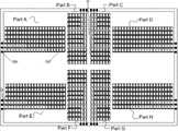
以一个5寸触摸屏为例说明本发明实施例提供的上述减少触控盲区的设计,在5寸触摸屏中需要的自电容电极04数量约为22*12=264个,如图6所示,为了将每个自电容电极04都引入至对应的导通连接点06处,且尽可能降低触控盲区的面积,可以将所有的自电容电极04共分为8个区域:PartA~PartH,在每个区域都需要将区域内的自电容电极04逐个连接至显示区域(Pane)下方的触控侦测芯片的连接端子08(FPC Bonding Pad)处,其中,如图7所示,在图7中每个区域均示出了3个自电容电极04,Part A区域的各自电容电极从Panel的左上方区域引出,经过Panel左边框引入至FPC Bonding Pad;Part B区域的各自电容电极从Panel的上方引出后,再从Panel的左边框引入至FPCBonding Pad;Panel C区域的各自电容电极从Panel的上方引出后,再从Panel的右边框引入至FPC Bonding Pad;Part D区域的各自电容电极从Panel的右上方引出后进过Panel的右边框引入至FPC Bonding Pad;同理,Part E区域的各自电容电极从Panel的左下方引出后,经过Panel的左边框引入至FPC BondingPad;Part F区域的各自电容电极从Panel的下方引出后直接连接至FPC BondingPad;Part G区域的各自电容电极从Panel的下方引出后直接连接至FPC BondingPad;Part H区域的各自电容电极从Panel的右下方引出,经过Panel右边框引入至FPC Bonding Pad。Taking a 5-inch touch screen as an example to illustrate the above-mentioned design for reducing touch blind areas provided by the embodiment of the present invention, the number of self-
具体地,为了便于观看图7仅示出了部分自电容电极04与导通连接点06的连接关系,从图7可以看出,位于显示区域两侧的Part A、Part D、Part E和Part H中触控盲区的大小约为3个亚像素单元的高度,在图7中用h表示,以5寸触摸屏中对应的像素单元的大小进行估算,触控盲区约为260μm,位于显示区域两侧的Part B、Part C、Part F和Part G中触控盲区的大小约为10个亚像素单元的宽度,在图7中用w表示,以5寸触摸屏中对应的像素单元的大小进行估算,触控盲区约为290μm。Specifically, for the convenience of viewing, FIG. 7 only shows the connection relationship between part of the self-
上述自电容电极04与导通连接点06的连接关系仅是举例说明,在实际设计时可以根据触摸屏的具体尺寸进行设计,为了最大化减少触控盲区的面积,可以将与各自电容电极04对应的导通连接点06分布在离自电容电极04距离最近的边框胶所在区域的侧边处,这样可以尽可能的缩短连接自电容电极04与导通连接点06之间的导线05的长度,以便尽可能的减少触控盲区的面积。The above-mentioned connection relationship between the self-
进一步地,为了彻底消除触摸屏中出现的触控盲区,可以将自电容电极04与导线05异层设置,导线05设置于上基板01与平坦层09之间,例如图8所示的可以将导线05设置于平坦层09和黑矩阵层03之间,且自电容电极04与对应的导线05通过过孔电性连接,这样在设计导线05的连接关系时可以采用传统的布线方式,如图9所示,即与所有自电容电极04连接的导线05都沿着一个方向延伸,且连接至设置在边框胶所在区域的同一个侧边区域内的对应的导通连接点06上。Further, in order to completely eliminate the touch blind area in the touch screen, the self-
进一步地,在本发明实施例提供的内嵌式触摸屏中,由于人体电容通过直接耦合的方式作用于各自电容电极04的自电容,因此,人体触碰屏幕时,仅在触摸位置下方的自电容电极04的电容值有较大的变化量,与触摸位置下方的自电容电极04相邻的自电容电极04的电容值变化量非常小,这样,在触摸屏上滑动时,不能确定自电容电极04所在区域内的触控坐标,为解决此问题,在本发明实施例提供的上述内嵌式触摸屏中,可以将相邻的两个自电容电极04相对的侧边均设置为折线,以便增大位于触摸位置下方的自电容电极04相邻的自电容电极04的电容值变化量。Further, in the in-cell touch screen provided by the embodiment of the present invention, since the human body capacitance acts on the self-capacitance of the respective
在具体实施时,可以采用如下两种方式之一或组合的方式设置各自电容电极04的整体形状:In specific implementation, the overall shape of the respective
1、可以将相邻的两个自电容电极04相对的为折线的侧边均设置为阶梯状结构,两阶梯状结构形状一致且相互匹配,如图10a所示,图10a中示出了2*2个自电容电极04;1. The sides opposite to the broken lines of the two adjacent self-
2、可以将相邻的两个自电容电极04相对的为折线的侧边均设置为凹凸状结构,两凹凸状结构形状一致且相互匹配,如图10b所示,图10b中示出了2*2个自电容电极04。2. The sides opposite to the broken lines of two adjacent self-
基于同一发明构思,本发明实施例还提供了一种显示装置,包括本发明实施例提供的上述内嵌式触摸屏,该显示装置可以为:手机、平板电脑、电视机、显示器、笔记本电脑、数码相框、导航仪等任何具有显示功能的产品或部件。该显示装置的实施可以参见上述内嵌式触摸屏的实施例,重复之处不再赘述。Based on the same inventive concept, an embodiment of the present invention also provides a display device, including the above-mentioned embedded touch screen provided by the embodiment of the present invention, the display device can be: a mobile phone, a tablet computer, a TV, a monitor, a notebook computer, a digital Any product or component with display function, such as photo frame and navigator. For the implementation of the display device, reference may be made to the above-mentioned embodiments of the embedded touch screen, and repeated descriptions will not be repeated.
本发明实施例提供的内嵌式触摸屏及显示装置,利用自电容的原理在触摸屏的上基板设置多个同层设置且相互绝缘的自电容电极,当人体未触碰屏幕时,各自电容电极所承受的电容为一固定值,当人体触碰屏幕时,对应的自电容电极所承受的电容为固定值叠加人体电容,触控侦测芯片在触控时间段通过检测各自电容电极的电容值变化可以判断出触控位置。由于人体电容可以作用于全部自电容,相对于人体电容仅能作用于互电容中的透射电容,由人体碰触屏幕所引起的触控变化量会比较大,因此能有效提高触控的信噪比,从而提高触控感应的准确性。并且,相对于采用互电容原理实现触控功能时需要在现有的阵列基板内增加两层新的膜层,本发明实施例提供的触摸屏中仅需要增加一层自电容电极即可实现触控功能,节省了生产成本,提高了生产效率。The embedded touch screen and display device provided by the embodiments of the present invention utilize the principle of self-capacitance to set a plurality of self-capacitance electrodes on the same layer and insulated from each other on the upper substrate of the touch screen. The capacitance withstanding is a fixed value. When the human body touches the screen, the capacitance of the corresponding self-capacitance electrode is a fixed value superimposed on the capacitance of the human body. The touch detection chip detects the capacitance value change of each capacitance electrode during the touch time period. The touch position can be determined. Since the human body capacitance can act on all self-capacitance, compared with the human body capacitance can only act on the transmission capacitance in the mutual capacitance, the amount of touch changes caused by the human body touching the screen will be relatively large, so the signal-to-noise of touch can be effectively improved Ratio, thereby improving the accuracy of touch sensing. Moreover, compared to the need to add two new film layers in the existing array substrate when the mutual capacitance principle is used to realize the touch function, the touch screen provided by the embodiment of the present invention only needs to add a layer of self-capacitance electrodes to realize touch control. Function, saving production cost and improving production efficiency.
进一步地,相对于自电容电极设置在上基板与平坦层之间时需要对平坦层进行构图露出与自电容电极的同层设置的导通连接点,该导通连接点通过边框胶与位于下基板的触控侦测芯片的连接端子电性连接,本发明实施例提供的触摸屏中由于自电容电极设置在上基板的平坦层与隔垫物层之间,因此,可以省去对平坦层进行构图,与自电容电极的同层设置的导通连接点即可直接通过边框胶与位于下基板的触控侦测芯片的连接端子电性连接,节省了制作工艺。Further, when the self-capacitance electrode is arranged between the upper substrate and the flat layer, it is necessary to pattern the flat layer to expose the conduction connection point provided on the same layer as the self-capacitance electrode. The connection terminals of the touch detection chip on the substrate are electrically connected. In the touch screen provided by the embodiment of the present invention, since the self-capacitance electrode is arranged between the flat layer of the upper substrate and the spacer layer, the flat layer can be omitted. Composition, the conduction connection point provided on the same layer as the self-capacitance electrode can be directly electrically connected to the connection terminal of the touch detection chip located on the lower substrate through the frame glue, which saves the manufacturing process.
显然,本领域的技术人员可以对本发明进行各种改动和变型而不脱离本发明的精神和范围。这样,倘若本发明的这些修改和变型属于本发明权利要求及其等同技术的范围之内,则本发明也意图包含这些改动和变型在内。Obviously, those skilled in the art can make various changes and modifications to the present invention without departing from the spirit and scope of the present invention. Thus, if these modifications and variations of the present invention fall within the scope of the claims of the present invention and their equivalent technologies, the present invention also intends to include these modifications and variations.
Claims (11)
Priority Applications (3)
| Application Number | Priority Date | Filing Date | Title |
|---|---|---|---|
| CN201410090141.7ACN103885660B (en) | 2014-03-12 | 2014-03-12 | A kind of In-cell touch panel and display device |
| PCT/CN2014/084550WO2015135289A1 (en) | 2014-03-12 | 2014-08-15 | Imbedded touchscreen and display device |
| US14/436,810US9830028B2 (en) | 2014-03-12 | 2014-08-15 | In-cell touch panel with self-capacitive electrodes and display device |
Applications Claiming Priority (1)
| Application Number | Priority Date | Filing Date | Title |
|---|---|---|---|
| CN201410090141.7ACN103885660B (en) | 2014-03-12 | 2014-03-12 | A kind of In-cell touch panel and display device |
Publications (2)
| Publication Number | Publication Date |
|---|---|
| CN103885660Atrue CN103885660A (en) | 2014-06-25 |
| CN103885660B CN103885660B (en) | 2016-04-06 |
Family
ID=50954587
Family Applications (1)
| Application Number | Title | Priority Date | Filing Date |
|---|---|---|---|
| CN201410090141.7AActiveCN103885660B (en) | 2014-03-12 | 2014-03-12 | A kind of In-cell touch panel and display device |
Country Status (3)
| Country | Link |
|---|---|
| US (1) | US9830028B2 (en) |
| CN (1) | CN103885660B (en) |
| WO (1) | WO2015135289A1 (en) |
Cited By (9)
| Publication number | Priority date | Publication date | Assignee | Title |
|---|---|---|---|---|
| CN104142772A (en)* | 2014-07-24 | 2014-11-12 | 京东方科技集团股份有限公司 | An embedded touch screen and display device |
| CN104166476A (en)* | 2014-07-28 | 2014-11-26 | 京东方科技集团股份有限公司 | Touch control display panel, control method of touch control display panel and touch control display device |
| CN104657022A (en)* | 2015-03-06 | 2015-05-27 | 京东方科技集团股份有限公司 | Display substrate and display device |
| CN104793387A (en)* | 2015-05-08 | 2015-07-22 | 上海中航光电子有限公司 | Display panel and display device |
| WO2015135289A1 (en)* | 2014-03-12 | 2015-09-17 | 京东方科技集团股份有限公司 | Imbedded touchscreen and display device |
| WO2015158083A1 (en)* | 2014-04-18 | 2015-10-22 | 京东方科技集团股份有限公司 | Touchscreen and display apparatus |
| CN106339031A (en)* | 2015-07-10 | 2017-01-18 | 夏普株式会社 | Image display device |
| CN106708339A (en)* | 2015-10-26 | 2017-05-24 | 京东方科技集团股份有限公司 | Embedded touch screen, driving method thereof and display device |
| CN107193153A (en)* | 2017-07-28 | 2017-09-22 | 武汉华星光电技术有限公司 | Colored filter of in-cell touch panel and preparation method thereof |
Families Citing this family (3)
| Publication number | Priority date | Publication date | Assignee | Title |
|---|---|---|---|---|
| CN103793120A (en)* | 2014-01-28 | 2014-05-14 | 北京京东方光电科技有限公司 | In cell touch panel and display device |
| CN104298409B (en)* | 2014-09-16 | 2017-05-03 | 京东方科技集团股份有限公司 | Touch screen and display device |
| US11449172B1 (en)* | 2021-06-25 | 2022-09-20 | Himax Technologies Limited | Touch control apparatus and touch panel thereof |
Citations (4)
| Publication number | Priority date | Publication date | Assignee | Title |
|---|---|---|---|---|
| KR20120017755A (en)* | 2010-08-19 | 2012-02-29 | 엘지디스플레이 주식회사 | LCD with Touch Sensor |
| US20120105347A1 (en)* | 2010-10-29 | 2012-05-03 | Sang-Jin Pak | Flat panel display with built-in touch sensors |
| CN103279244A (en)* | 2013-06-06 | 2013-09-04 | 敦泰科技有限公司 | Capacitive touch screen |
| CN103294322A (en)* | 2013-06-06 | 2013-09-11 | 敦泰科技有限公司 | Touch control display device |
Family Cites Families (4)
| Publication number | Priority date | Publication date | Assignee | Title |
|---|---|---|---|---|
| CN103123548B (en)* | 2011-11-18 | 2016-12-07 | 宸鸿科技(厦门)有限公司 | Touch control display apparatus |
| TW201350974A (en)* | 2012-06-08 | 2013-12-16 | Inv Element Inc | In-cell touch display panel system with increased accuracy of touch positions |
| JP2015180979A (en)* | 2012-07-31 | 2015-10-15 | シャープ株式会社 | Touch panel and manufacturing method of touch panel |
| CN103885660B (en)* | 2014-03-12 | 2016-04-06 | 京东方科技集团股份有限公司 | A kind of In-cell touch panel and display device |
- 2014
- 2014-03-12CNCN201410090141.7Apatent/CN103885660B/enactiveActive
- 2014-08-15USUS14/436,810patent/US9830028B2/enactiveActive
- 2014-08-15WOPCT/CN2014/084550patent/WO2015135289A1/enactiveApplication Filing
Patent Citations (4)
| Publication number | Priority date | Publication date | Assignee | Title |
|---|---|---|---|---|
| KR20120017755A (en)* | 2010-08-19 | 2012-02-29 | 엘지디스플레이 주식회사 | LCD with Touch Sensor |
| US20120105347A1 (en)* | 2010-10-29 | 2012-05-03 | Sang-Jin Pak | Flat panel display with built-in touch sensors |
| CN103279244A (en)* | 2013-06-06 | 2013-09-04 | 敦泰科技有限公司 | Capacitive touch screen |
| CN103294322A (en)* | 2013-06-06 | 2013-09-11 | 敦泰科技有限公司 | Touch control display device |
Cited By (15)
| Publication number | Priority date | Publication date | Assignee | Title |
|---|---|---|---|---|
| US9830028B2 (en) | 2014-03-12 | 2017-11-28 | Boe Technology Group Co., Ltd. | In-cell touch panel with self-capacitive electrodes and display device |
| WO2015135289A1 (en)* | 2014-03-12 | 2015-09-17 | 京东方科技集团股份有限公司 | Imbedded touchscreen and display device |
| WO2015158083A1 (en)* | 2014-04-18 | 2015-10-22 | 京东方科技集团股份有限公司 | Touchscreen and display apparatus |
| US9823789B2 (en) | 2014-04-18 | 2017-11-21 | Boe Technology Group Co., Ltd. | Touch display panel and display device |
| US9665222B2 (en) | 2014-07-24 | 2017-05-30 | Boe Technology Group Co., Ltd. | In-cell touch panel and display device with self-capacitance electrodes |
| CN104142772A (en)* | 2014-07-24 | 2014-11-12 | 京东方科技集团股份有限公司 | An embedded touch screen and display device |
| CN104166476A (en)* | 2014-07-28 | 2014-11-26 | 京东方科技集团股份有限公司 | Touch control display panel, control method of touch control display panel and touch control display device |
| US10001867B2 (en) | 2014-07-28 | 2018-06-19 | Boe Technology Group Co., Ltd. | Touch display panel and method for controlling the same, and touch display device |
| WO2016141703A1 (en)* | 2015-03-06 | 2016-09-15 | 京东方科技集团股份有限公司 | Display panel and display device |
| CN104657022A (en)* | 2015-03-06 | 2015-05-27 | 京东方科技集团股份有限公司 | Display substrate and display device |
| CN104793387A (en)* | 2015-05-08 | 2015-07-22 | 上海中航光电子有限公司 | Display panel and display device |
| CN106339031A (en)* | 2015-07-10 | 2017-01-18 | 夏普株式会社 | Image display device |
| CN106708339A (en)* | 2015-10-26 | 2017-05-24 | 京东方科技集团股份有限公司 | Embedded touch screen, driving method thereof and display device |
| CN106708339B (en)* | 2015-10-26 | 2023-12-15 | 京东方科技集团股份有限公司 | An embedded touch screen, its driving method and display device |
| CN107193153A (en)* | 2017-07-28 | 2017-09-22 | 武汉华星光电技术有限公司 | Colored filter of in-cell touch panel and preparation method thereof |
Also Published As
| Publication number | Publication date |
|---|---|
| US9830028B2 (en) | 2017-11-28 |
| CN103885660B (en) | 2016-04-06 |
| WO2015135289A1 (en) | 2015-09-17 |
| US20160188031A1 (en) | 2016-06-30 |
Similar Documents
| Publication | Publication Date | Title |
|---|---|---|
| CN103885660B (en) | A kind of In-cell touch panel and display device | |
| CN103793120A (en) | In cell touch panel and display device | |
| CN103970392B (en) | A kind of touch screen and display device | |
| CN104020912B (en) | Capacitive touch structure, embedded touch screen, display device and scanning method of display device | |
| CN104020906B (en) | A kind of In-cell touch panel and display device | |
| CN104020905B (en) | A kind of In-cell touch panel and display device | |
| CN104022127B (en) | A kind of array base palte and preparation method thereof and display device | |
| CN104035640B (en) | A kind of In-cell touch panel and display device | |
| CN104020907B (en) | In cell touch panel and display device | |
| CN104142772B (en) | Embedded type touch screen and display device | |
| CN104503633B (en) | A kind of In-cell touch panel, its driving method and display device | |
| CN104020913A (en) | Embedded touch screen and display device | |
| CN104020893B (en) | A kind of In-cell touch panel and display device | |
| CN104022128B (en) | Array substrate, manufacturing method thereof and displaying device | |
| CN104020910B (en) | A kind of In-cell touch panel and display device | |
| CN104536637A (en) | Embedded touch screen and display device | |
| CN104020891A (en) | In cell touch panel and display device | |
| WO2015180315A1 (en) | Capacitive touch structure, embedded touchscreen, display device and scanning method therefor | |
| CN104536629A (en) | An embedded touch screen and display device | |
| CN103926729A (en) | Array substrate, color film substrate, touch display device and driving method thereof | |
| CN104020911A (en) | In cell touch panel and display device | |
| CN104035639B (en) | Capacitance touch structure, In-cell touch panel, display device and scan method thereof | |
| CN106154612A (en) | Embedded touch panel |
Legal Events
| Date | Code | Title | Description |
|---|---|---|---|
| C06 | Publication | ||
| PB01 | Publication | ||
| C10 | Entry into substantive examination | ||
| SE01 | Entry into force of request for substantive examination | ||
| C14 | Grant of patent or utility model | ||
| GR01 | Patent grant |