CN103885274A - Light emitting device and related projection system - Google Patents
Light emitting device and related projection systemDownload PDFInfo
- Publication number
- CN103885274A CN103885274ACN201210558409.6ACN201210558409ACN103885274ACN 103885274 ACN103885274 ACN 103885274ACN 201210558409 ACN201210558409 ACN 201210558409ACN 103885274 ACN103885274 ACN 103885274A
- Authority
- CN
- China
- Prior art keywords
- light
- wavelength conversion
- area
- emitting device
- heat
- Prior art date
- Legal status (The legal status is an assumption and is not a legal conclusion. Google has not performed a legal analysis and makes no representation as to the accuracy of the status listed.)
- Granted
Links
Images

Landscapes
- Projection Apparatus (AREA)
- Arrangement Of Elements, Cooling, Sealing, Or The Like Of Lighting Devices (AREA)
- Non-Portable Lighting Devices Or Systems Thereof (AREA)
Abstract
Description
Translated fromChinese技术领域technical field
本发明涉及照明及显示技术领域,特别是涉及一种发光装置及相关投影系统。The invention relates to the technical field of illumination and display, in particular to a light emitting device and a related projection system.
背景技术Background technique
利用激发荧光粉来产生的彩色光作为光源是一种在投影显示等领域应用广泛的方案。一般来说,荧光粉会被设置在一个高速旋转的色轮上,激光等激发光入射到色轮并激发荧光粉产生受激光,同时产生大量热量,色轮的高速转动的作用在于使得不同区域的荧光粉会轮流处于激发光的照射下,不同区域可以分担热量,从而降低色轮温度。Using colored light generated by exciting phosphors as a light source is a solution widely used in projection display and other fields. Generally speaking, the phosphor will be set on a high-speed rotating color wheel. Exciting light such as laser light is incident on the color wheel and excites the phosphor to generate the stimulated light. At the same time, a large amount of heat is generated. The high-speed rotation of the color wheel is to make different areas The phosphor powder will be exposed to the excitation light in turn, and different regions can share the heat, thereby reducing the temperature of the color wheel.
由于荧光粉对激发光的转换效率并不是100%,荧光粉会产生大量的热,而色轮的散热是主要通过色轮与空气之间的热对流实现的。尽管色轮暴露在空气中可以将热量传导至空气而降低工作温度,但是由于空气存在大量的灰尘颗粒,当色轮表面附着有灰尘颗粒,灰尘颗粒的周围会集聚大量的热量,有可能导致色轮的温度急剧升高,甚至烧坏色轮。Since the conversion efficiency of the phosphor powder to the excitation light is not 100%, the phosphor powder will generate a lot of heat, and the heat dissipation of the color wheel is mainly realized through the heat convection between the color wheel and the air. Although the color wheel exposed to the air can transfer heat to the air to lower the working temperature, but because there are a lot of dust particles in the air, when there are dust particles attached to the surface of the color wheel, a large amount of heat will accumulate around the dust particles, which may cause color loss. The temperature of the wheel rises sharply, and even burns out the color wheel.
发明内容Contents of the invention
本发明主要解决的技术问题是提供了一种兼顾波长转换装置的防尘和有效降低波长转换装置的工作温度的发光装置及相关投影系统。The main technical problem to be solved by the present invention is to provide a light emitting device and a related projection system that take into account both the dustproof of the wavelength conversion device and the effective reduction of the working temperature of the wavelength conversion device.
本发明实施例提供了发光装置,包括:An embodiment of the present invention provides a light emitting device, including:
一种激发光源,用于产生激发光;An excitation light source for generating excitation light;
波长转换装置,包括波长转换层,该波长转换层用于吸收激发光并出射受激光;A wavelength conversion device, including a wavelength conversion layer, the wavelength conversion layer is used to absorb the excitation light and emit the received light;
驱动装置,驱动装置用于驱动波长转换层周期性转动,以使得激发光入射在波长转换层上的光斑沿预定圆形轨迹周期性运动,波长转换装置的至少部分区域的线速度大于等于75米/秒;A driving device, the driving device is used to drive the wavelength conversion layer to periodically rotate, so that the spot of the excitation light incident on the wavelength conversion layer moves periodically along a predetermined circular trajectory, and the linear velocity of at least a part of the wavelength conversion device is greater than or equal to 75 meters /Second;
密封装置,波长转换装置设置于该密封装置内,该密封装置包括透光区和导热区,透光区用于透射从波长转换装置出射到该透光区的光,导热区与波长转换装置的光出射面或者与该光出射面相对的表面之间的距离小于等于1毫米,导热区用于将波长转换装置传递至该导热区的热量传导至密封装置外部,且导热区的面积大于等于激发光入射在波长转换层的光斑的面积。A sealing device, the wavelength conversion device is arranged in the sealing device, the sealing device includes a light transmission area and a heat conduction area, the light transmission area is used to transmit the light emitted from the wavelength conversion device to the light transmission area, and the heat conduction area and the wavelength conversion device The distance between the light exit surface or the surface opposite to the light exit surface is less than or equal to 1 mm, the heat conduction area is used to conduct the heat transferred from the wavelength conversion device to the heat conduction area to the outside of the sealing device, and the area of the heat conduction area is greater than or equal to the excitation The area of the spot where light is incident on the wavelength conversion layer.
优选地,导热区位于密封装置上与光斑相对的位置。Preferably, the heat conduction area is located on the sealing device at a position opposite to the light spot.
优选地,导热区的面积与波长转换装置的靠近导热区的表面的面积相等。Preferably, the area of the heat conduction region is equal to the area of the surface of the wavelength conversion device close to the heat conduction region.
优选地,驱动装置固定在密封装置的侧壁上。Preferably, the drive means are fixed on the side walls of the sealing means.
优选地,波长转换装置还包括基板,该基板用于承载波长转换层,基板位于波长转换层的靠近导热区的一侧。Preferably, the wavelength conversion device further includes a substrate for carrying the wavelength conversion layer, and the substrate is located on a side of the wavelength conversion layer close to the heat conduction region.
优选地,基板的导热系数大于所述波长转换层的导热系数。Preferably, the thermal conductivity of the substrate is greater than the thermal conductivity of the wavelength conversion layer.
优选地,波长转换装置的基板上设置有反射层,该反射层将入射到该反射层的光反射至波长转换装置的光出射面。Preferably, a reflective layer is disposed on the substrate of the wavelength conversion device, and the reflective layer reflects the light incident on the reflective layer to the light exit surface of the wavelength conversion device.
优选地,发光装置还包括散热装置,散热装置用于加快导热区的热量传递至外界空气中。Preferably, the light emitting device further includes a heat dissipation device, which is used to accelerate the transfer of heat from the heat conduction area to the outside air.
本发明还提供了一种投影系统,包括上述的发光装置。The present invention also provides a projection system, including the above light emitting device.
与现有技术相比,本发明实施例具有如下有益效果:Compared with the prior art, the embodiments of the present invention have the following beneficial effects:
本发明实施例中,波长转换装置位于密封装置内,因此波长转换装置不会出现被灰尘附着的情况。当波长转换装置的光出射面或者与该光出射面相对的表面与导热区之间的距离小于等于1毫米,且波长转换层上至少部分区域的线速度大于等于75米/秒,该至少部分区域会对波长转换装置与密封装置之间的空气层产生一个较大的剪切力,使得较薄的空气层内的空气产生扰动,并导致该空气层的热阻相对于静止时空气层的热阻会急剧下降,波长转换装置的热量可以很快地通过空气层传导至密封装置的导热区,并由导热区将热量导出密封装置,从而有效降低了波长转换装置的工作温度,实现了兼顾了防尘和有效降低波长转换装置的工作温度。In the embodiment of the present invention, the wavelength conversion device is located in the sealing device, so the wavelength conversion device will not be attached by dust. When the distance between the light exit surface of the wavelength conversion device or the surface opposite to the light exit surface and the heat conduction area is less than or equal to 1 mm, and the linear velocity of at least part of the wavelength conversion layer is greater than or equal to 75 m/s, the at least part The region will generate a large shear force on the air layer between the wavelength conversion device and the sealing device, which will cause the air in the thinner air layer to turbulence, and cause the thermal resistance of the air layer to be higher than that of the air layer at rest. The thermal resistance will drop sharply, and the heat of the wavelength conversion device can be quickly conducted to the heat conduction area of the sealing device through the air layer, and the heat will be exported from the heat transfer area to the sealing device, thereby effectively reducing the working temperature of the wavelength conversion device and achieving both In order to prevent dust and effectively reduce the working temperature of the wavelength conversion device.
附图说明Description of drawings
图1为本发明发光装置的一个实施例的结构示意图;FIG. 1 is a schematic structural view of an embodiment of a light-emitting device of the present invention;
图2为图1所示实施例中波长转换装置与密封装置的导热区之间的Fig. 2 is the distance between the wavelength conversion device and the heat conduction region of the sealing device in the embodiment shown in Fig. 1
热阻与二者之间的距离的关系示意图;Schematic diagram of the relationship between thermal resistance and the distance between them;
图3为本发明发光装置的又一个实施例的结构示意图;3 is a schematic structural view of another embodiment of the light emitting device of the present invention;
图4为本发明发光装置的又一个实施例的结构示意图;Fig. 4 is a structural schematic diagram of another embodiment of the light emitting device of the present invention;
图5为本发明发光装置的又一个实施例的结构示意图。Fig. 5 is a schematic structural diagram of another embodiment of the light emitting device of the present invention.
具体实施方式Detailed ways
下面结合附图及实施方式来对本发明的实施例进行详细分析。The embodiments of the present invention will be analyzed in detail below in conjunction with the accompanying drawings and implementation methods.
实施例一:Embodiment one:
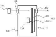
图1为本发明发光装置的一个实施例的结构示意图,如图1所示,发光装置包括激发光源110、波长转换装置120、驱动装置130、密封装置140。FIG. 1 is a schematic structural diagram of an embodiment of the light emitting device of the present invention. As shown in FIG.
激发光源110具体为激光光源,可以产生激光以作为激发波长转换材料的激发光。当然,在本发明其它实施方式中,激发光源110还可以是LED光源等。The
波长转换装置120包括波长转换层121。波长转换层121设置有波长转换材料,波长转换材料可以吸收光源110出射的激发光并出射受激光。本实施例中的波长转换材料具体为荧光粉,在本发明其它实施方式中,波长转换材料还可以是量子点、荧光染料等具有波长转换能力的材料,并不限于荧光粉。The
驱动装置130可以驱动波长转换装置120周期性转动,以使得激发光入射在波长转换层上的光斑沿预定圆形轨迹周期性运动,从而该圆形轨迹的各个部分可以分摊热量。优选地,波长转换装置120呈圆盘状,波长转换层121呈与该圆盘同心的环状,驱动装置130为呈圆柱形的马达,并且驱动装置130与波长转换装置120同轴固定。The
为了对波长转换装置120进行防尘,波长转换装置120设置于一密封装置140内,该密封装置140包括导热区141、透光区142和入光区143。In order to protect the
本实施例中,透光区142是在密封装置140的侧壁上设置的一透明区域,该透明区域可以透射从波长转换装置120出射到透光区142的光。具体地,透光区142设置有玻璃或者PMMA(Polymethylmethacrylate,聚甲基丙烯酸甲酯)等透明材料。在本发明的其它实施方式中,透光区142还可以是设置滤光片,同时实现对波长转换装置的出射光中的不同波长的光进行选择性过滤。类似地,入光区143也是密封装置的侧壁上设置的一透明区域,与透光区142的不同点在于,入光区143设置在激发光源110和波长转换装置140之间的光路上,可以透射激发光源110的出射光。In this embodiment, the light-transmitting
本领域人员所公知的是,波长转换装置的波长转换材料对激发光吸收会产生大量的热量,而波长转换装置的热量首先传导给密封装置内的空气,然后密封装置140内的空气传导给密封装置140,最终由密封装置140将热量散发到外界空气中的。波长转换装置120与密封装置140之间的空气层越薄,热阻越小,并且热阻和空气层的厚度呈线性关系,因此波长转换装置120与密封装置140之间的距离越小,它们二者之间的热阻越小,该热阻与该距离呈线性关系。但是即使波长转换装置120与密封装置140的距离很小,空气层的热阻依然很大。Those skilled in the art know that the wavelength conversion material of the wavelength conversion device will generate a lot of heat when the excitation light is absorbed, and the heat of the wavelength conversion device is first transmitted to the air in the sealing device, and then the air in the
这里,通过实验对密封装置140中的波长转换装置120的散热进行研究。根据实验,当波长转换装置120的转速设置为6000转/分钟,波长转换装置的直径等于30厘米,为了更好的进行散热,密封装置140外壁除入光区143和透光区142外的其它区域为金属材料以作为导热区141,此时波长转换装置120与密封装置140的导热区141之间的热阻与二者之间的距离的关系如图2所示,当波长转换装置120与密封装置140的导热区141之间的距离大于1毫米时,二者之间的热阻与距离基本上呈线性关系,且距离越小,波长转换装置120与密封装置140的导热区141之间的热阻越小;当波长转换装置120与密封装置140的导热区141之间的距离小于等于1毫米时,随着距离减小,二者之间的热阻不再与距离呈线性关系,而是急剧减小,这是与现有认知不同的。Here, the heat dissipation of the
实验发现,当波长转换装置120与密封装置140的导热区141之间距离减小到1毫米以下,二者之间的空气层的热量传导方式发生了变化:空气层内的空气会产生扰动,导致热阻急剧的下降,而不再仅仅是通过热对流来传热,而这种扰动是由于高速旋转的波长转换装置120对空气层的产生剪切力引起的。Experiments have found that when the distance between the
本实施例中波长转换装置的直径为30厘米而转速为6000转/分钟,此时波长转换装置120的最外围区域的转速为188米/秒,而通过改变波长转换装置120的直径和转速进行一系列实验发现,只需波长转换装置120的部分区域的线速度达到75米/秒,且波长转换装置120与导热区141之间的距离小于等于1毫米,就可以达到大大降低波长转换装置120和密封装置140之间的空气层的热阻的效果。In this embodiment, the diameter of the wavelength conversion device is 30 centimeters and the rotational speed is 6000 rpm. At this time, the rotational speed of the outermost region of the
上述实验中,密封装置140除了入光区143和透光区142之外的区域设置为金属材料作为导热区141,而通过实验,保持其它条件不变,只改变导热区面积与位置发现,即使只在密封装置140的内表面与波长转换装置120相对的区域设置导热材料依然具有良好效果。进一步减小导热区的面积发现,只需要设置一个与波长转换装置120相对导热区,且保证该导热区的面积大于等于波长转换装置的入射光斑的面积,同时满足波长转换装置的部分区域的线速度达到75米/秒,且波长转换装置120与导热区之间的距离小于等于1毫米,就能够实现良好的散热,从而可以有效降低波长转换装置120的工作温度,以实现兼顾了防尘和有效降低波长转换装置120的工作温度。In the above experiment, the area of the
本实施例中的导热区141的金属材料具体为铝板,铝板是一种高导热材料,具有良好的热的传导能力。导热区141可以将波长转换装置120传递至该导热区141的热量传导至密封装置140外部。在本发明的其它实施方式中,导热区141可以设置铜、银等金属导热材料,也可以设置氧化铝、氮化铝、氮化镓、金刚石薄膜等陶瓷导热材料,还可以设置半导体制冷器等冷却装置,都可以起到热量传递的作用。The metal material of the
值得说明的是,本实施例中的波长转换装置120的光出射面与导热区141是平行设置的,但是由于误差等原因,二者可能不是完全平行的,只要保证二者之间的最大距离小于等于1毫米即可。这里的光出射面是指波长转换装置120用于出射受激光或者受激光与激发光的混合光的表面,本实施例中具体为波长转换层121靠近导热区141的表面。当然,容易理解的是,波长转换装置120的光出射面和导热区141越接近平行,二者的距离就可以设置的越小,越有利于散热。It is worth noting that the light emitting surface of the
本实施例中,驱动装置130优选地是液压轴承马达,液压轴承马达具有寿命长、噪声低的优点,更重要的是,液压轴承马达具有良好的转动平稳性,可以使得波长转换装置的光出射面和导热区之间的距离可以靠的更近。In this embodiment, the driving
本实施例中波长转换装置120还包括基板122,该基板122为透明玻璃,可以对波长转换层121起到支撑作用。优选地,基板122的表面设置一层滤光膜,该滤光膜可以透射激发光而反射受激光,可以提高受激光的利用率;进一步地,滤光膜可以透射小角度入射的激发光而反射受激光和大角度的激发光,可以同时提高激发光和受激光利用率。但是在波长转换层本身刚性足够的情况下(例如波长转换层是通过将荧光粉掺杂在透明玻璃中形成的),基板是可以省略的,此时滤光膜可以镀在波长转换层的表面,同样具有相同的效果。In this embodiment, the
本实施例中,导热区141设置在密封装置140上远离激发光光斑的位置,但是当导热区141设置有蓝宝石、氮化镓、金刚石薄膜等透明导热材料时,导热区141可以设置在透光区142的位置,此时透光区和导热区合为一个区域。In this embodiment, the
实施例二Embodiment two
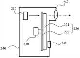
图3为本发明发光装置的又一个实施例的结构示意图,如图3所示,发光装置包括激发光源210、波长转换装置220、驱动装置230、密封装置240。波长转换装置220包括波长转换层221和基板222。密封装置240包括导热区241和透光区242。FIG. 3 is a schematic structural diagram of another embodiment of the light emitting device of the present invention. As shown in FIG. The
本实施例的发光装置与图1所示的发光装置的不同点在于:The difference between the light emitting device of this embodiment and the light emitting device shown in FIG. 1 lies in:
(1)本实施例中的导热区241的面积较小,其面积等于光斑的面积,此时依然能够保证实现对波长转换装置220的导热,同时由于只需要对导热区241的表面进行加工使其平整度较高,而密封装置240的其它区域不需要,可以密封装置240的降低成本。(1) The area of the
(2)本实施例中的激发光源210设置在密封装置240的内部,密封装置240可以对光源起到防尘的作用,并且密封装置240不需要设置入光区。容易理解是,其它元件也可以设置于密封装置240内。(2) The
(3)本实施例中,发光装置的透光区242为一个透镜。由于荧光粉等波长转换材料的出射光为全角发光,需要设置透镜进行收集以减小其发散角度。为了提高透镜242的收集效果,透镜242需要距离波长转换层的比较近,因此透镜242设置于密封装置240内,且用来收集波长转换装置220的出射光,此时透镜242可以设置在距离波长转换装置220较近的位置,并且容易固定。(3) In this embodiment, the light-transmitting
实施例三Embodiment Three
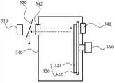
图4为本发明发光装置的又一个实施例的结构示意图,如图4所示,发光装置包括激发光源310、波长转换装置320、驱动装置330、密封装置340。波长转换装置320包括波长转换层321和基板322。密封装置340包括导热区341和透光区342。FIG. 4 is a schematic structural diagram of another embodiment of the light emitting device of the present invention. As shown in FIG. The wavelength conversion device 320 includes a
本实施例中的发光装置与图1所示的发光装置的不同点在于:The difference between the light emitting device in this embodiment and the light emitting device shown in FIG. 1 lies in:
(1)波长转换装置320为反射式色轮,基板322的表面设置有反射层,该反射层设置于基板322靠近波长转换层321的一面,可以反射入射到该反射层的出射光。激发光从透光区342透射至波长转换装置320,波长转换装置320的出射光也从透光区342透射出密封装置340。由于波长转换层321和基板322是紧密接触的,波长转换层321的热量可以很容易传导到基板322上,波长转换层321的光出射面和基板322远离波长转换层321的表面的温度非常接近,因此本实施例中,基板322远离波长转换层的表面,即波长转换装置320的与光出射面相对的表面,与导热区341的距离小于等于1毫米时,也可以有效的降低波长转换装置320的工作温度。(1) The wavelength conversion device 320 is a reflective color wheel, and the surface of the substrate 322 is provided with a reflective layer. The reflective layer is provided on the side of the substrate 322 close to the
本实施例中,波长转换装置320的基板322靠近密封装置340的导热区341。基板相对于荧光粉等波长转换材料,表面平整度可以做到更高,因此基板322和导热区341之间的距离可以更小。优选地,基板材料的导热系数高于波长转换材料的导热系数,此时波长转换装置320的热量更容易传导至导热区341。例如,基板322为金属材料,金属具有较高的导热系数,同时便于机械加工并可以获得较高的表面平整度。In this embodiment, the substrate 322 of the wavelength converting device 320 is close to the
另外,基板322也可以是高反铝板等具有高反射性表面的硬质材料,此时反射层和基板的其它部分可以看作一个整体。为了区分激发光和波长转换装置出射光的光路,发光装置还设置了滤光片350来进行分光。In addition, the substrate 322 may also be a hard material with a highly reflective surface such as a high-reflective aluminum plate. In this case, the reflective layer and other parts of the substrate may be regarded as a whole. In order to distinguish the optical paths of the excitation light and the light emitted by the wavelength conversion device, the light emitting device is further provided with a
(2)对反射式的波长转换装置来说,导热区341的位置设置可以更加优化。本实施例中,导热区341设置在密封装置340与基板322靠近的表面上,且位于该表面上与波长转换层上的激发光光斑相对的位置。很明显,波长转换装置320上温度最高的区域是激发光光斑所在的区域,因此这里的导热区341的位置使得热量更迅速地从波长转换装置320传导至导热区341。当然,前述实施例一提到导热区341可以设置成透明的导热材料,也同样可以位于密封装置的侧壁与激发光光斑相对的位置,同样可以更有效地散热,但透明导热材料的成本要比一般导热材料无疑要高很多。(2) For a reflective wavelength conversion device, the position setting of the
(3)本实施例中,驱动装置330固定于密封装置340的侧壁上。这种固定方式更容易实现波长转换装置320和导热区341之间具有较小的空气间隙。若驱动装置和密封装置不相对固定,例如图1所示的驱动装置,装配时一般需要精密的调节才能将波长转换装置与密封装置靠得很近。而相对固定时,比较容易直接通过机械件的精度保证两者之间有一个很小的空气间隙。(3) In this embodiment, the driving
实施例四Embodiment Four
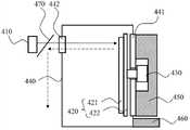
图5为本发明发光装置的又一个实施例的结构示意图,如图5所示,发光装置包括激发光源410、波长转换装置420、驱动装置430、密封装置440、滤光片470。波长转换装置420包括波长转换层421和基板422。密封装置440包括导热区441和透光区442。FIG. 5 is a schematic structural diagram of another embodiment of the light emitting device of the present invention. As shown in FIG. The
本实施例的发光装置与图4所示的发光装置的不同点在于:The difference between the light emitting device of this embodiment and the light emitting device shown in FIG. 4 lies in:
(1)本实施例中的导热区441的面积大于入射到波长转换层的激发光光斑的面积,而与基板422的面积相接近。容易理解的是,导热区441的面积越大,热传导能力越强。考虑到兼顾导热区441的材料成本和导热能力,导热区441的面积与波长转换装置420的靠近导热区441的表面的面积相等,具体在本实施例中,也就是导热区441的面积与基板422的面积相等。(1) The area of the
(2)本实施例中,发光装置还包括散热装置450,该散热装置450紧靠第一外表面,第一外表面为导热区441所在的密封装置的侧壁的外表面。散热装置450具体为散热器,其包括散热鳍片和连接散热鳍片与第一外表面的热管,实际上热管就是间接与导热区441相连接,加快导热区441的热量传递,从而间接加快波长转换装置420的热量传递。进一步,发光装置还可以设置风扇460,该风扇460也设置在密封装置440的第一外表面上,可以对着散热器吹风,以加快散热器的散热。当然,散热鳍片和风扇460也都可以不设置在第一外表面上,而设置在其它表面上,同样可以起到加快导热区441散热的作用。(2) In this embodiment, the light emitting device further includes a
另一方面,由于驱动装置430与波长转换装置420是固定连接的,因此波长转换装置420的热量会传导至驱动装置430,驱动装置430的温度也会很高。而这里,驱动装置430是固定在导热区所在的侧壁上,其在第一外表面的凸出部分会对周围的散热鳍片产生热对流而可以加快驱动装置430的散热。进一步地,驱动装置430的非转动部件可以与散热鳍片相接触,使得驱动装置430的散热更快。类似地,设置于第一外表面的风扇460也同样可以加快驱动装置430的散热。On the other hand, since the
本说明书中各个实施例采用递进的方式描述,每个实施例重点说明的都是与其他实施例的不同之处,各个实施例之间相同相似部分互相参见即可。Each embodiment in this specification is described in a progressive manner, each embodiment focuses on the difference from other embodiments, and the same and similar parts of each embodiment can be referred to each other.
本发明实施例还提供一种投影系统,包括发光装置,该发光装置可以具有上述各实施例中的结构与功能。该投影系统可以采用各种投影技术,例如液晶显示器(LCD,Liquid Crystal Display)投影技术、数码光路处理器(DLP,Digital Light Processor)投影技术。An embodiment of the present invention also provides a projection system, including a light emitting device, and the light emitting device may have the structures and functions in the above-mentioned embodiments. The projection system can adopt various projection technologies, such as liquid crystal display (LCD, Liquid Crystal Display) projection technology, digital light path processor (DLP, Digital Light Processor) projection technology.
以上所述仅为本发明的实施方式,并非因此限制本发明的专利范围,凡是利用本发明说明书及附图内容所作的等效结构或等效流程变换,或直接或间接运用在其他相关的技术领域,均同理包括在本发明的专利保护范围内。The above is only the embodiment of the present invention, and does not limit the patent scope of the present invention. Any equivalent structure or equivalent process conversion made by using the description of the present invention and the contents of the accompanying drawings, or directly or indirectly used in other related technologies fields, all of which are equally included in the scope of patent protection of the present invention.
Claims (10)
Priority Applications (2)
| Application Number | Priority Date | Filing Date | Title |
|---|---|---|---|
| CN201810408028.7ACN108646508B (en) | 2012-12-20 | 2012-12-20 | Light emitting device and related projection system |
| CN201210558409.6ACN103885274B (en) | 2012-12-20 | 2012-12-20 | Lighting device and related projection system |
Applications Claiming Priority (1)
| Application Number | Priority Date | Filing Date | Title |
|---|---|---|---|
| CN201210558409.6ACN103885274B (en) | 2012-12-20 | 2012-12-20 | Lighting device and related projection system |
Related Child Applications (1)
| Application Number | Title | Priority Date | Filing Date |
|---|---|---|---|
| CN201810408028.7ADivisionCN108646508B (en) | 2012-12-20 | 2012-12-20 | Light emitting device and related projection system |
Publications (2)
| Publication Number | Publication Date |
|---|---|
| CN103885274Atrue CN103885274A (en) | 2014-06-25 |
| CN103885274B CN103885274B (en) | 2018-05-15 |
Family
ID=50954236
Family Applications (2)
| Application Number | Title | Priority Date | Filing Date |
|---|---|---|---|
| CN201210558409.6AActiveCN103885274B (en) | 2012-12-20 | 2012-12-20 | Lighting device and related projection system |
| CN201810408028.7AActiveCN108646508B (en) | 2012-12-20 | 2012-12-20 | Light emitting device and related projection system |
Family Applications After (1)
| Application Number | Title | Priority Date | Filing Date |
|---|---|---|---|
| CN201810408028.7AActiveCN108646508B (en) | 2012-12-20 | 2012-12-20 | Light emitting device and related projection system |
Country Status (1)
| Country | Link |
|---|---|
| CN (2) | CN103885274B (en) |
Cited By (15)
| Publication number | Priority date | Publication date | Assignee | Title |
|---|---|---|---|---|
| CN104676492A (en)* | 2015-01-31 | 2015-06-03 | 杨毅 | Wavelength conversion device and light emitting device |
| CN105068367A (en)* | 2015-08-04 | 2015-11-18 | 杨毅 | Light-emitting device, projection display device and lamp |
| CN105301750A (en)* | 2015-10-12 | 2016-02-03 | 杨毅 | Optical module, light emitting device and projection display device |
| CN105301881A (en)* | 2015-10-12 | 2016-02-03 | 杨毅 | Light emitting device and projection display device |
| EP3043200A1 (en)* | 2014-12-08 | 2016-07-13 | Delta Electronics, Inc. | Color wheel device |
| CN106200222A (en)* | 2014-12-08 | 2016-12-07 | 台达电子工业股份有限公司 | Color wheel device |
| CN106324956A (en)* | 2015-06-30 | 2017-01-11 | 海信集团有限公司 | Laser light source heat dissipation system and laser projection system |
| CN106444241A (en)* | 2015-08-04 | 2017-02-22 | 海信集团有限公司 | Laser light source and laser projection display device |
| CN106444239A (en)* | 2015-08-04 | 2017-02-22 | 杨毅 | Illuminating device, lighting fitting, projection display device |
| CN108693685A (en)* | 2017-04-06 | 2018-10-23 | 精工爱普生株式会社 | Light supply apparatus and projecting apparatus |
| CN109581796A (en)* | 2015-10-14 | 2019-04-05 | 海信集团有限公司 | A kind of fluorescent wheel and laser light source |
| CN111033366A (en)* | 2017-08-17 | 2020-04-17 | 索尼公司 | Light source device and projection type display device |
| CN112666780A (en)* | 2019-10-15 | 2021-04-16 | 台达电子工业股份有限公司 | Wavelength conversion device |
| CN114518650A (en)* | 2018-04-12 | 2022-05-20 | 深圳光峰科技股份有限公司 | Color wheel assembly, light source system and projection equipment |
| US11753999B2 (en) | 2021-06-17 | 2023-09-12 | General Electric Company | Gas turbine sensor assembly and associated shutter mechanism |
Citations (9)
| Publication number | Priority date | Publication date | Assignee | Title |
|---|---|---|---|---|
| JP2001100309A (en)* | 1999-09-27 | 2001-04-13 | Hitachi Ltd | Device for preventing noise of rotating body, rotating color filter unit, and projection system using the same |
| US20020003704A1 (en)* | 2000-05-25 | 2002-01-10 | Hideki Ohmae | Color wheel assembly and color sequential display device using the same, color wheel unit and color sequential display device using the same, and color sequential display device |
| CN1725100A (en)* | 2004-07-19 | 2006-01-25 | 精碟科技股份有限公司 | color wheel set |
| CN2812047Y (en)* | 2005-03-31 | 2006-08-30 | 联想(北京)有限公司 | Dust-proof protector for color wheel of projector |
| US20080049345A1 (en)* | 2006-08-28 | 2008-02-28 | Minebea Co., Ltd. | Color wheel unit |
| JP2008225407A (en)* | 2007-03-16 | 2008-09-25 | Seiko Epson Corp | projector |
| WO2010116444A1 (en)* | 2009-03-30 | 2010-10-14 | Necディスプレイソリューションズ株式会社 | Projection type display device |
| CN102305386A (en)* | 2008-01-29 | 2012-01-04 | 绎立锐光科技开发(深圳)有限公司 | Light source structure and method for improving light conversion efficiency based on fluorescent powder |
| CN202549931U (en)* | 2011-11-25 | 2012-11-21 | 深圳市光峰光电技术有限公司 | Wavelength conversion device and light emitting device |
Family Cites Families (1)
| Publication number | Priority date | Publication date | Assignee | Title |
|---|---|---|---|---|
| CN102455580A (en)* | 2010-10-21 | 2012-05-16 | 中强光电股份有限公司 | Heat dissipation module for projection optical system |
- 2012
- 2012-12-20CNCN201210558409.6Apatent/CN103885274B/enactiveActive
- 2012-12-20CNCN201810408028.7Apatent/CN108646508B/enactiveActive
Patent Citations (9)
| Publication number | Priority date | Publication date | Assignee | Title |
|---|---|---|---|---|
| JP2001100309A (en)* | 1999-09-27 | 2001-04-13 | Hitachi Ltd | Device for preventing noise of rotating body, rotating color filter unit, and projection system using the same |
| US20020003704A1 (en)* | 2000-05-25 | 2002-01-10 | Hideki Ohmae | Color wheel assembly and color sequential display device using the same, color wheel unit and color sequential display device using the same, and color sequential display device |
| CN1725100A (en)* | 2004-07-19 | 2006-01-25 | 精碟科技股份有限公司 | color wheel set |
| CN2812047Y (en)* | 2005-03-31 | 2006-08-30 | 联想(北京)有限公司 | Dust-proof protector for color wheel of projector |
| US20080049345A1 (en)* | 2006-08-28 | 2008-02-28 | Minebea Co., Ltd. | Color wheel unit |
| JP2008225407A (en)* | 2007-03-16 | 2008-09-25 | Seiko Epson Corp | projector |
| CN102305386A (en)* | 2008-01-29 | 2012-01-04 | 绎立锐光科技开发(深圳)有限公司 | Light source structure and method for improving light conversion efficiency based on fluorescent powder |
| WO2010116444A1 (en)* | 2009-03-30 | 2010-10-14 | Necディスプレイソリューションズ株式会社 | Projection type display device |
| CN202549931U (en)* | 2011-11-25 | 2012-11-21 | 深圳市光峰光电技术有限公司 | Wavelength conversion device and light emitting device |
Cited By (22)
| Publication number | Priority date | Publication date | Assignee | Title |
|---|---|---|---|---|
| US9897795B2 (en) | 2014-12-08 | 2018-02-20 | Delta Electronics, Inc. | Color wheel device |
| EP3043200A1 (en)* | 2014-12-08 | 2016-07-13 | Delta Electronics, Inc. | Color wheel device |
| CN106200222A (en)* | 2014-12-08 | 2016-12-07 | 台达电子工业股份有限公司 | Color wheel device |
| CN106200222B (en)* | 2014-12-08 | 2018-02-09 | 台达电子工业股份有限公司 | color wheel device |
| CN104676492A (en)* | 2015-01-31 | 2015-06-03 | 杨毅 | Wavelength conversion device and light emitting device |
| CN106324956A (en)* | 2015-06-30 | 2017-01-11 | 海信集团有限公司 | Laser light source heat dissipation system and laser projection system |
| US10317782B2 (en) | 2015-08-04 | 2019-06-11 | Hisense Co., Ltd. | Laser light source and laser projection display device |
| CN106444241A (en)* | 2015-08-04 | 2017-02-22 | 海信集团有限公司 | Laser light source and laser projection display device |
| CN106444239A (en)* | 2015-08-04 | 2017-02-22 | 杨毅 | Illuminating device, lighting fitting, projection display device |
| CN105068367A (en)* | 2015-08-04 | 2015-11-18 | 杨毅 | Light-emitting device, projection display device and lamp |
| CN105301750A (en)* | 2015-10-12 | 2016-02-03 | 杨毅 | Optical module, light emitting device and projection display device |
| CN105301881A (en)* | 2015-10-12 | 2016-02-03 | 杨毅 | Light emitting device and projection display device |
| CN109581796A (en)* | 2015-10-14 | 2019-04-05 | 海信集团有限公司 | A kind of fluorescent wheel and laser light source |
| CN108693685A (en)* | 2017-04-06 | 2018-10-23 | 精工爱普生株式会社 | Light supply apparatus and projecting apparatus |
| CN111033366A (en)* | 2017-08-17 | 2020-04-17 | 索尼公司 | Light source device and projection type display device |
| CN111033366B (en)* | 2017-08-17 | 2023-02-28 | 索尼公司 | Light source device and projection type display device |
| CN114518650A (en)* | 2018-04-12 | 2022-05-20 | 深圳光峰科技股份有限公司 | Color wheel assembly, light source system and projection equipment |
| US11822052B2 (en) | 2018-04-12 | 2023-11-21 | Appotronics Corporation Limited | Colour wheel assembly, light source system, and projection device |
| CN112666780A (en)* | 2019-10-15 | 2021-04-16 | 台达电子工业股份有限公司 | Wavelength conversion device |
| US11353168B2 (en) | 2019-10-15 | 2022-06-07 | Delta Electronics, Inc. | Wavelength conversion device |
| CN112666780B (en)* | 2019-10-15 | 2022-06-24 | 台达电子工业股份有限公司 | wavelength conversion device |
| US11753999B2 (en) | 2021-06-17 | 2023-09-12 | General Electric Company | Gas turbine sensor assembly and associated shutter mechanism |
Also Published As
| Publication number | Publication date |
|---|---|
| CN108646508B (en) | 2021-06-08 |
| CN103885274B (en) | 2018-05-15 |
| CN108646508A (en) | 2018-10-12 |
Similar Documents
| Publication | Publication Date | Title |
|---|---|---|
| CN103885274B (en) | Lighting device and related projection system | |
| JP6259906B2 (en) | Wavelength converter and related light emitting device | |
| JP5970661B2 (en) | Wavelength conversion member, light source, and automotive headlamp | |
| JP6786546B2 (en) | Wavelength converter, light emitting device and projection system | |
| JP6096937B2 (en) | Light emitting device and related projection system | |
| CN103969934B (en) | A compact light source system | |
| TWI651580B (en) | Wavelength conversion device and projector | |
| CN102818170B (en) | light source | |
| CN103838068B (en) | Light-emitting device and relevant projecting system thereof | |
| CN105737103A (en) | Wavelength conversion device, relevant fluorescent color wheel and relevant projection device | |
| TWI617059B (en) | Illumination system and wavelength-converting deivce thereof | |
| CN114815483B (en) | Transmission type wavelength conversion member and laser light source | |
| CN105676578B (en) | A kind of light-source system of compact conformation | |
| JP5949872B2 (en) | Fluorescent light source device | |
| JP6413673B2 (en) | Fluorescent light source device | |
| WO2020048101A1 (en) | Wavelength conversion device and light source system | |
| TWI719706B (en) | Wavelength conversion unit and lighting device | |
| CN102455446B (en) | Brightness enhancement film, optical wavelength conversion wheel assembly with brightness enhancement film and light source | |
| JP2015161882A (en) | Light emitting device for projector | |
| WO2019153638A1 (en) | Wavelength conversion device | |
| JP2013093268A (en) | Wavelength conversion type light source device | |
| US11041614B2 (en) | Wavelength conversion unit and lighting device | |
| CN213630088U (en) | Light converter heat radiation structure | |
| CN205003433U (en) | Illuminator , projection display equipment and lamps and lanterns | |
| CN116224693A (en) | Color wheel assembly and projection device |
Legal Events
| Date | Code | Title | Description |
|---|---|---|---|
| C06 | Publication | ||
| PB01 | Publication | ||
| C10 | Entry into substantive examination | ||
| SE01 | Entry into force of request for substantive examination | ||
| GR01 | Patent grant | ||
| GR01 | Patent grant | ||
| CP01 | Change in the name or title of a patent holder | ||
| CP01 | Change in the name or title of a patent holder | Address after:518000 20-22, 20-22 headquarters building, 63 high tech Zone, Xuefu Road, Nanshan District, Guangdong Province, Guangdong. Patentee after:APPOTRONICS Corp.,Ltd. Address before:518000 20-22, 20-22 headquarters building, 63 high tech Zone, Xuefu Road, Nanshan District, Guangdong Province, Guangdong. Patentee before:SHENZHEN GUANGFENG TECHNOLOGY Co.,Ltd. | |
| CP03 | Change of name, title or address | ||
| CP03 | Change of name, title or address | Address after:518000 20-22, 20-22 headquarters building, 63 high tech Zone, Xuefu Road, Nanshan District, Guangdong Province, Guangdong. Patentee after:SHENZHEN GUANGFENG TECHNOLOGY Co.,Ltd. Address before:518057 Guangfeng Photoelectric Technology Co., Ltd., Shenzhen Integrated Circuit Design and Application Industrial Park, 1089 Chaguang Road, Xili Town, Nanshan District, Shenzhen City, Guangdong Province Patentee before:APPOTRONICS Corp.,Ltd. |