CN103872937A - Control method of flying capacitive type five-level inverter device - Google Patents
Control method of flying capacitive type five-level inverter deviceDownload PDFInfo
- Publication number
- CN103872937A CN103872937ACN201410125395.8ACN201410125395ACN103872937ACN 103872937 ACN103872937 ACN 103872937ACN 201410125395 ACN201410125395 ACN 201410125395ACN 103872937 ACN103872937 ACN 103872937A
- Authority
- CN
- China
- Prior art keywords
- power switch
- level
- inverter
- state
- amplitude
- Prior art date
- Legal status (The legal status is an assumption and is not a legal conclusion. Google has not performed a legal analysis and makes no representation as to the accuracy of the status listed.)
- Granted
Links
Images


Landscapes
- Inverter Devices (AREA)
Abstract
Description
Translated fromChinese技术领域technical field
本发明涉及并网发电用逆变器技术领域,具体是一种飞跨电容型五电平逆变装置的控制方法。The invention relates to the technical field of inverters for grid-connected power generation, in particular to a control method for a flying capacitor type five-level inverter.
背景技术Background technique
近年来,多电平逆变器在高压大功率领域应用越来越多,现在应用较为成熟的主要有三种拓扑结构:二极管钳位型、级联型和飞跨电容型。二极管钳位型多电平逆变器拓扑有直流母线侧各电容电压均压困难和电压应力不均匀等缺点。级联型多电平逆变器拓扑在需提供有功功率场合,需要多个独立直流电源且不共地。飞跨电容型多电平逆变器拓扑和其他两种相比,利用电容钳位,克服了二极管钳位型逆变器的固有缺陷;利用一个直流电源,克服了级联型逆变器的多电源缺陷;并有大量的冗余开关状态,具有更容易向多电平发展的优良特点。In recent years, multi-level inverters have been used more and more in high-voltage and high-power fields. Now there are three main topologies that are relatively mature: diode clamped, cascaded, and flying capacitor. The diode-clamped multilevel inverter topology has the disadvantages of difficult voltage equalization and uneven voltage stress of each capacitor on the DC bus side. The cascaded multi-level inverter topology requires multiple independent DC power sources without sharing ground when active power needs to be provided. Compared with the other two, the flying-capacitor multilevel inverter topology overcomes the inherent defects of the diode-clamped inverter by using the capacitor clamp; it overcomes the inherent defects of the cascade inverter by using a DC power supply Multiple power supply defects; and there are a large number of redundant switch states, which have the excellent characteristics of easier development to multi-level.
多电平脉宽调制(Pulse Width Modulation,PWM)技术是多电平逆变器研究的核心技术。多电平逆变器脉宽调制技术的原理是用正弦波作为调制波,以恒定频率的三角波为载波,由于三角波的上下宽度是线性变化的,通过正弦调制波与三角波进行比较,可以得到一组幅值相等而宽度正比于正弦波的矩形脉冲序列,用开关量取代模拟量,并通过逆变开关管的通断控制,把直流电能变换成多电平PWM交流电能。Multilevel pulse width modulation (Pulse Width Modulation, PWM) technology is the core technology of multilevel inverter research. The principle of multi-level inverter pulse width modulation technology is to use a sine wave as the modulating wave and a triangular wave with a constant frequency as the carrier. Since the upper and lower widths of the triangular wave change linearly, a comparison between the sine wave and the triangular wave can be obtained. Set a rectangular pulse sequence with equal amplitude and width proportional to the sine wave, replace the analog quantity with the switch value, and convert the DC power into a multi-level PWM AC power through the on-off control of the inverter switch tube.
PWM调制的控制目的主要有两个:There are two main purposes of PWM modulation control:
一、对输出电压的控制;1. Control the output voltage;
二、对多电平逆变器自身运行状态的控制。Second, the control of the operating state of the multi-level inverter itself.
PWM调制技术包括载波PWM方法和空间矢量PWM方法。如下所示:PWM modulation techniques include carrier PWM method and space vector PWM method. As follows:

多电平逆变器的PWM控制,必须和其电路结构紧密联系,根据不同电路的不同特点,设计不同的应用方法。主要的载波方法有载波同相层叠PWM方法(PDPWM)、载波反相层叠PWM方法(APOD PWM)和载波移相PWM方法(PSPWM)等。其中载波同相层叠PWM方法(PDPWM)被广泛认为具有最低的线电压谐波性能,并且实现简单。但将PDPWM方法应用于飞跨电容型逆变器时,会造成电容上电压变化,而飞跨电容型逆变器利用电容钳位,必须保证电容上电压稳定,因此传统PDPWM方法不适用于飞跨电容型多电平逆变器。The PWM control of the multi-level inverter must be closely related to its circuit structure, and different application methods should be designed according to the different characteristics of different circuits. The main carrier methods include carrier in-phase stacked PWM method (PDPWM), carrier anti-phase stacked PWM method (APOD PWM) and carrier phase-shifted PWM method (PSPWM). Among them, the carrier in-phase stacked PWM method (PDPWM) is widely considered to have the lowest line voltage harmonic performance and is simple to implement. However, when the PDPWM method is applied to a flying-capacitor inverter, the voltage on the capacitor will change, and the flying-capacitor inverter uses capacitor clamping to ensure that the voltage on the capacitor is stable. Therefore, the traditional PDPWM method is not suitable for flying capacitor inverters. Transcapacitive multilevel inverter.
飞跨电容型多电平逆变器只有载波移相PWM方法(PSPWM)适用,但将传统PSPWM方法应用于飞跨电容型多电平逆变器时,由于此算法固有特点,将在逆变器输出侧产生较大的线电压谐波,不利于发电并网;由于飞跨电容电压自动平衡,不能人为干预和调整,会使飞跨电容电压有一定的电压偏差,且无法改变。Only the carrier phase-shift PWM method (PSPWM) is applicable to the flying capacitor type multilevel inverter, but when the traditional PSPWM method is applied to the flying capacitor type multilevel inverter, due to the inherent characteristics of this algorithm, it will Large line voltage harmonics are generated on the output side of the inverter, which is not conducive to power generation and grid connection; due to the automatic balance of the flying capacitor voltage, human intervention and adjustment cannot be performed, which will cause a certain voltage deviation of the flying capacitor voltage and cannot be changed.
发明内容Contents of the invention
针对上述问题,本发明的目的是提供一种飞跨电容型五电平逆变装置的控制方法,通过载波层叠算法获得逆变器运行状态,在“1”,“0”,“-1”电平时增加电平选择环节,合理分配电平向量,利用飞跨电容型逆变装置特有的冗余状态平衡飞跨电容电压,降低输出线电压谐波。In view of the above problems, the object of the present invention is to provide a control method for a flying capacitor type five-level inverter device, which obtains the operating state of the inverter through the carrier cascading algorithm, at "1", "0", "-1" Increase the level selection link when leveling, rationally distribute the level vector, use the unique redundant state of the flying capacitor inverter device to balance the flying capacitor voltage, and reduce the output line voltage harmonics.
本发明采用如下技术方案:The present invention adopts following technical scheme:
一种适用于飞跨电容型五电平逆变器的改进的载波层叠PWM控制方法,其特点在于该方法包括下列具体步骤:An improved carrier stacked PWM control method suitable for flying capacitor type five-level inverters, characterized in that the method includes the following specific steps:
步骤①、逆变控制模块设定飞跨电容型五电平逆变装置输出电平状态及开关组合状态,当飞跨电容型五电平逆变装置的输出电压为+Vdc/2,+Vdc/4,0,-Vdc/4,-Vdc/2时(Vdc为直流电源电压),分别定义逆变装置对应输出为“2”,“1”,“0”,“-1”,“-2”电平状态,其开关组合状态如下表,“1”代表闭合此开关,“0”代表关断此开关:

步骤②、逆变控制模块根据上位机给定的载波频率F1,产生幅值为0.5且恒定的四层三角载波;
逆变控制模块根据上位机给定的所述的飞跨电容型五电平逆变装置输出侧电压幅值及频率要求,产生恒定的正弦调制波,频率为F2;The inverter control module generates a constant sinusoidal modulation wave with a frequency of F2 according to the voltage amplitude and frequency requirements of the output side of the flying capacitor type five-level inverter device given by the host computer;
步骤③、逆变控制模块根据载波频率F1及调制波频率F2,计算预设参数K,具体过程为:
首先计算单个调制周期中“0”电平出现次数n=F1/F2+1:First calculate the number of "0" level occurrences n=F1/F2+1 in a single modulation cycle:
当n为偶数时,K=n;When n is an even number, K=n;
当n为奇数时,K=(n-3)/2;When n is an odd number, K=(n-3)/2;
步骤④、逆变控制模块利用载波同相层叠方法,将步骤②得到的正弦调制波与四层三角载波进行比较,产生八个功率开关管开关信号,具体方法如下:In
当正弦调制波的幅值比第一层三角载波的幅值大时,八个功率开关管状态为11110000,逆变器输出“2”电平状态;When the amplitude of the sinusoidal modulation wave is greater than the amplitude of the first layer of triangular carrier, the state of the eight power switches is 11110000, and the inverter outputs a "2" level state;
当正弦调制波幅值介于第一、二层三角载波幅值之间时,八个功率开关管状态为11101000、01110001、10110010或11010100,四个电压向量各作用1/2调制波周期,交替循环,逆变器输出“1”电平状态;When the amplitude of the sinusoidal modulation wave is between the amplitude of the first and second triangular carrier waves, the states of the eight power switches are 11101000, 01110001, 10110010 or 11010100, and each of the four voltage vectors acts on 1/2 of the modulation wave cycle, alternately Circulation, the inverter outputs "1" level state;
当正弦调制波幅值介于第二、三层三角载波幅值之间时,逆变器输出“0”电平状态,八个功率开关管状态计算方法如下:When the amplitude of the sinusoidal modulation wave is between the second and third layer triangular carrier amplitudes, the inverter outputs a "0" level state, and the calculation method for the state of the eight power switch tubes is as follows:
根据初始开关信号,记录“0”电平计数个数M,将M与预先设定参数K相模:According to the initial switch signal, record the "0" level count number M, and compare M with the preset parameter K:
当模值小于等于K/2-1时,八个功率管开关状态为00110011、10010110或01010101,三个电压向量各作用1个调制波周期,交替循环,逆变装置输出“0+”状态;When the modulus value is less than or equal to K/2-1, the switching states of the eight power tubes are 00110011, 10010110 or 01010101, and each of the three voltage vectors acts on one modulation wave cycle, alternating cycles, and the inverter device outputs "0+" state;
当模值大于K/2-1时,八个功率管开关状态为11001100、10101010或01101001,三个电压向量各作用1个调制波周期,交替循环,逆变装置输出“0-”状态;When the modulus value is greater than K/2-1, the switching states of the eight power tubes are 11001100, 10101010 or 01101001, and each of the three voltage vectors acts on one modulation wave cycle, alternating cycles, and the inverter device outputs "0-" state;
当正弦调制波幅值介于第三、四层三角载波幅值之间时,八个功率开关管状态为10001110、01001101、00101011或00010111,四个电压向量各作用1/2调制波周期,交替循环,逆变器输出“-1”电平状态;When the amplitude of the sine modulation wave is between the amplitude of the third and fourth triangular carrier waves, the state of the eight power switch tubes is 10001110, 01001101, 00101011 or 00010111, and each of the four voltage vectors acts on 1/2 of the modulation wave cycle, alternately cycle, the inverter outputs "-1" level state;
当正弦调制波的幅值比第四层三角载波幅值小时,八个功率开关管状态为00001111,逆变器输出“-2”电平状态;:When the amplitude of the sinusoidal modulation wave is smaller than the amplitude of the fourth-layer triangular carrier, the state of the eight power switches is 00001111, and the inverter outputs a "-2" level state;:
步骤⑤、根据步骤④产生的开关信号,逆变控制模块将信号发送给各功率开关管,并驱动各功率开关管的开通和关断。Step ⑤. According to the switch signal generated in
步骤⑥、重复执行步骤④~步骤⑤,保证稳定的正弦波输出。
与现有技术相比,本发明的特点如下:Compared with prior art, characteristics of the present invention are as follows:
1)改进本不适用于飞跨电容型五电平逆变器的载波同相层叠PWM方法使之适用;1) Improve the carrier in-phase stacked PWM method that is not applicable to the flying capacitor type five-level inverter to make it applicable;
2)具有更低的线电压谐波,更有利于逆变器并网运行;2) It has lower line voltage harmonics, which is more conducive to the grid-connected operation of the inverter;
3)灵活度大,实现简单,对硬件要求低;3) Great flexibility, simple implementation, and low hardware requirements;
4)增加电平选择环节,可以人为控制飞跨电容上的电压平衡,具有更好的控制性能;4) Increase the level selection link, which can artificially control the voltage balance on the flying capacitor, and has better control performance;
5)飞跨电容型逆变器相比传统二极管钳位型逆变器,利用飞跨电容代替了复杂的钳位二极管,减少了器件数目。由于飞跨电容的存在,可以对有功和无功功率进行解耦控制,有利于逆变器并网。飞跨电容型逆变器开关冗余状态较多,容易推广到更高电平应用。5) Compared with traditional diode-clamped inverters, flying-capacitor inverters use flying-capacitors instead of complex clamping diodes, reducing the number of components. Due to the existence of the flying capacitor, the active and reactive power can be decoupled and controlled, which is beneficial to the grid connection of the inverter. The flying-capacitor inverter has many switch redundant states, and it is easy to be extended to higher level applications.
附图说明Description of drawings
图1为飞跨电容型五电平逆变主电路结构图,包含直流母线与一条桥臂;Figure 1 is a structural diagram of the main circuit of the flying capacitor type five-level inverter, including a DC bus and a bridge arm;
图2为载波同相层叠五电平调制图;Figure 2 is a carrier in-phase stacked five-level modulation diagram;
图3为本发明改进的载波同相层叠PWM方法流程图;Fig. 3 is the flow chart of the carrier in-phase stacked PWM method improved by the present invention;
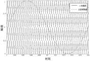
图4为飞跨电容上的电压仿真图;Figure 4 is a voltage simulation diagram on the flying capacitor;
图5为改进的载波同相层叠PWM方法(PDPWM)与载波移相PWM方法(PSPWM)线电压谐波比较图。Figure 5 is a comparison diagram of line voltage harmonics between the improved carrier in-phase stacked PWM method (PDPWM) and the carrier phase-shift PWM method (PSPWM).
具体实施方式Detailed ways
下面结合附图与实施例对本发明做进一步说明,但不应以此限制本发明的保护范围。The present invention will be further described below in conjunction with the accompanying drawings and embodiments, but the protection scope of the present invention should not be limited thereby.
图1为采用改进载波层叠PWM方法(PDPWM)的飞跨电容型五电平逆变器的单相电路系统,它包括直流电源1,直流母线2,飞跨电容3,逆变桥4,滤波电感5和逆变控制模块6。Figure 1 shows the single-phase circuit system of the flying-capacitor five-level inverter using the improved carrier-carrier stacked PWM method (PDPWM), which includes a
所述的直流母线2由四个电容C1、C2、C3和C4串联而成,即第一电容C1的正极与直流电源1的正极连接,负极与第二电容C2的正极连接;所述的第三电容C3的正极与所述的第二电容C2的负极连接,负极与所述的第四电容C4的正极连接;所述的第四电容的负极与直流电源1的负极连接。从而提供五种不同的电平。The
所述的逆变桥4由三条结构相同桥臂组成,每条桥臂包含由八个功率开关管、八个功率二极管构成的开关电路和由飞跨电容3构成的钳位电路。The
所述的开关电路包含八个功率开关管和八个功率二极管,连接如下(以第一桥臂为例):The switch circuit includes eight power switch tubes and eight power diodes, connected as follows (take the first bridge arm as an example):
功率开关管之间连接:Connection between power switch tubes:
第一功率开关管Sa1的集电极与直流母线的正极连接;The collector of the first power switchSa1 is connected to the positive pole of the DC bus;
第一功率开关管Sa1的发射极与第二功率开关管Sa2的集电极连接;The emitter of the first power switch tubeSa1 is connected to the collector of the second power switch tubeSa2 ;
第二功率开关管Sa2的发射极与第三功率开关管Sa3的集电极连接;The emitter of the second power switch Sa2 is connected to the collector of the third power switch Sa3 ;
第三功率开关管Sa3的发射极与第四功率开关管Sa4的集电极连接;The emitter of the third power switch Sa3 is connected to the collector of the fourth power switch Sa4 ;
第四功率开关管Sa4的发射极与第五功率开关管Sa5的集电极连接;The emitter of the fourth power switch tube Sa4 is connected to the collector of the fifth power switch tube Sa5 ;
第五功率开关管Sa5的发射极与第六功率开关管Sa6的集电极连接;The emitter of the fifth power switch tubeSa5 is connected to the collector of the sixth power switch tubeSa6 ;
第六功率开关管Sa6的发射极与第七功率开关管Sa7的集电极连接;The emitter of the sixth power switch Sa6 is connected to the collector of the seventh power switch Sa7 ;
第七功率开关管Sa7的发射极与第八功率开关管Sa8的集电极连接;The emitter of the seventh power switch tube Sa7 is connected to the collector of the eighth power switch tube Sa8 ;
第八功率开关管Sa8的发射极与直流母线的负极连接。The emitter of the eighth power switch Sa8 is connected to the negative pole of the DC bus.
功率开关管与功率二极管连接:The power switch tube is connected to the power diode:
第一功率开关管Sa1与第一功率二极管VD1并联,即第一功率开关管Sa1的集电极与第一功率二极管VD1的阴极连接,第一功率开关管Sa1的发射极与第一功率二极管VD1的阳极连接;The first power switchSa1 is connected in parallel with the first power diodeVD1 , that is, the collector of the first power switchSa1 is connected to the cathode of the first power diodeVD1 , and the emitter of the first power switch Sa1 is connected to the first power switchSa1 . Anode connection of a power diode VD1 ;
第二功率开关管Sa2与第二功率二极管VD2并联;The second power switch tubeSa2 is connected in parallel with the second power diodeVD2 ;
第三功率开关管Sa3与第三功率二极管VD3并联;The third power switch tube Sa3 is connected in parallel with the third power diode VD3 ;
第四功率开关管Sa4与第四功率二极管VD4并联;The fourth power switch tube Sa4 is connected in parallel with the fourth power diode VD4 ;
第五功率开关管Sa5与第四功率二极管VD5并联;The fifth power switch tube Sa5 is connected in parallel with the fourth power diode VD5 ;
第六功率开关管Sa6与第四功率二极管VD6并联;The sixth power switch tube Sa6 is connected in parallel with the fourth power diode VD6 ;
第七功率开关管Sa7与第四功率二极管VD7并联;The seventh power switch tube Sa7 is connected in parallel with the fourth power diode VD7 ;
第八功率开关管Sa8与第四功率二极管VD8并联;The eighth power switch tube Sa8 is connected in parallel with the fourth power diode VD8 ;
所述的钳位电路为:The clamping circuit is:
第一功率管Sa1的发射极与飞跨电容C7的正极连接;The emitter of the first power transistorSa1 is connected to the positive pole of the flying capacitorC7 ;
第七功率管Sa7的发射极与飞跨电容C7的负极连接;The emitter of the seventh power transistor Sa7 is connected to the negative pole of the flying capacitor C7 ;
第二功率管Sa2的发射极与飞跨电容C6的正极连接;The emitter of the second power transistorSa2 is connected to the positive pole of the flying capacitorC6 ;
第六功率管Sa6的发射极与飞跨电容C6的负极连接;The emitter of the sixth power transistor Sa6 is connected to the negative pole of the flying capacitor C6 ;
第三功率管Sa3的发射极与飞跨电容C5的正极连接;The emitter of the third power transistorSa3 is connected to the positive pole of the flying capacitorC5 ;
第五功率管Sa5的发射极与飞跨电容C5的负极连接;The emitter of the fifth power transistorSa5 is connected to the negative pole of the flying capacitorC5 ;
所述的功率开关管为绝缘栅双极型晶体管IGBT或大功率晶体管GTR。The power switch tube is an insulated gate bipolar transistor IGBT or a high-power transistor GTR.
所述的滤波电感5为绕线式电感。The filter inductor 5 is a wire-wound inductor.
所述的逆变控制模块6是数字信号处理器、单片机或计算机。逆变控制模块6的控制信号输出端分别与所述的功率单元的功率管的控制端(基极)相连,该逆变控制模块的输入端与上位机相连。功率开关管的控制信号由逆变控制模块提供。The
一种适用于飞跨电容型五电平逆变器的改进的载波层叠PWM控制方法,其特点在于该方法包括下列具体步骤:An improved carrier stacked PWM control method suitable for flying capacitor type five-level inverters, characterized in that the method includes the following specific steps:
步骤①、逆变控制模块6设定飞跨电容型五电平逆变装置输出电平状态及开关组合状态,当飞跨电容型五电平逆变装置的输出电压为+Vdc/2,+Vdc/4,0,-Vdc/4,-Vdc/2时(Vdc为直流电源电压),分别定义逆变装置对应输出为“2”,“1”,“0”,“-1”,“-2”电平状态,其开关组合状态如下表,“1”代表闭合此开关,“0”代表关断此开关:

步骤②、逆变控制模块6根据上位机给定的载波频率F1,产生幅值为0.5且恒定的四层三角载波;
逆变控制模块6根据上位机给定的所述的飞跨电容型五电平逆变装置输出侧电压幅值及频率要求,产生恒定的正弦调制波,频率为F2;The
步骤③、逆变控制模块6根据载波频率F1及调制波频率F2,计算预设参数K,具体过程为:
首先计算单个调制周期中“0”电平出现次数n=F1/F2+1:First calculate the number of "0" level occurrences n=F1/
当n为偶数时,K=n;When n is an even number, K=n;
当n为奇数时,K=(n-3)/2;When n is an odd number, K=(n-3)/2;
步骤④、逆变控制模块6利用载波同相层叠方法,将步骤②得到的正弦调制波与四层三角载波进行比较,产生八个功率开关管开关信号,具体方法如下:In
当正弦调制波的幅值比第一层三角载波的幅值大时,八个功率开关管状态为11110000,逆变器输出“2”电平状态;When the amplitude of the sinusoidal modulation wave is greater than the amplitude of the first layer of triangular carrier, the state of the eight power switches is 11110000, and the inverter outputs a "2" level state;
当正弦调制波幅值介于第一、二层三角载波幅值之间时,八个功率开关管状态为11101000、01110001、10110010或11010100,四个电压向量各作用1/2调制波周期,交替循环,逆变器输出“1”电平状态;When the amplitude of the sinusoidal modulation wave is between the amplitude of the first and second triangular carrier waves, the states of the eight power switches are 11101000, 01110001, 10110010 or 11010100, and each of the four voltage vectors acts on 1/2 of the modulation wave cycle, alternately Circulation, the inverter outputs "1" level state;
当正弦调制波幅值介于第二、三层三角载波幅值之间时,逆变器输出“0”电平状态,八个功率管开关状态计算方法如下:When the amplitude of the sinusoidal modulation wave is between the second and third layer triangular carrier amplitudes, the inverter outputs a "0" level state, and the calculation method of the eight power tube switch states is as follows:
根据初始开关信号,记录“0”电平计数个数M,将M与预先设定参数K相模:According to the initial switch signal, record the "0" level count number M, and compare M with the preset parameter K:
当模值小于等于K/2-1时,八个功率开关管状态为00110011、10010110或01010101,三个电压向量各作用1个调制波周期,交替循环,逆变装置输出“0+”状态;When the modulus value is less than or equal to K/2-1, the state of the eight power switch tubes is 00110011, 10010110 or 01010101, and each of the three voltage vectors acts on one modulation wave cycle, alternating cycles, and the inverter device outputs "0+" state;
当模值大于K/2-1时,八个功率开关管状态为11001100、10101010或01101001,三个电压向量各作用1个调制波周期,交替循环,逆变装置输出“0-”状态;When the modulus value is greater than K/2-1, the states of the eight power switch tubes are 11001100, 10101010 or 01101001, and each of the three voltage vectors acts on one modulation wave period, alternating cycles, and the inverter device outputs "0-" state;
当正弦调制波幅值介于第三、四层三角载波幅值之间时,八个功率开关管状态为10001110、01001101、00101011或00010111,四个电压向量各作用1/2调制波周期,交替循环,逆变器输出“-1”电平状态;When the amplitude of the sine modulation wave is between the amplitude of the third and fourth triangular carrier waves, the state of the eight power switch tubes is 10001110, 01001101, 00101011 or 00010111, and each of the four voltage vectors acts on 1/2 of the modulation wave cycle, alternately cycle, the inverter outputs "-1" level state;
当正弦调制波的幅值比第四层三角载波幅值小时,八个功率开关管状态为00001111,逆变器输出“-2”电平状态;:When the amplitude of the sinusoidal modulation wave is smaller than the amplitude of the fourth-layer triangular carrier, the state of the eight power switches is 00001111, and the inverter outputs a "-2" level state;:
步骤⑤、根据步骤④产生的开关信号,逆变控制模块6将信号发送给各功率开关管,并驱动各功率开关管的开通和关断。Step ⑤. According to the switch signal generated in
步骤⑥、重复执行步骤④~步骤⑤,保证稳定的正弦波输出。
Claims (1)
Translated fromChinesePriority Applications (1)
| Application Number | Priority Date | Filing Date | Title |
|---|---|---|---|
| CN201410125395.8ACN103872937B (en) | 2014-03-31 | 2014-03-31 | A kind of control method of striding capacitance type five level inverter |
Applications Claiming Priority (1)
| Application Number | Priority Date | Filing Date | Title |
|---|---|---|---|
| CN201410125395.8ACN103872937B (en) | 2014-03-31 | 2014-03-31 | A kind of control method of striding capacitance type five level inverter |
Publications (2)
| Publication Number | Publication Date |
|---|---|
| CN103872937Atrue CN103872937A (en) | 2014-06-18 |
| CN103872937B CN103872937B (en) | 2016-03-02 |
Family
ID=50911141
Family Applications (1)
| Application Number | Title | Priority Date | Filing Date |
|---|---|---|---|
| CN201410125395.8AActiveCN103872937B (en) | 2014-03-31 | 2014-03-31 | A kind of control method of striding capacitance type five level inverter |
Country Status (1)
| Country | Link |
|---|---|
| CN (1) | CN103872937B (en) |
Cited By (9)
| Publication number | Priority date | Publication date | Assignee | Title |
|---|---|---|---|---|
| CN106100430A (en)* | 2016-08-23 | 2016-11-09 | 合肥工业大学 | The carrier wave implementation method of three-phase five-level inverter low common-mode voltage modulation |
| CN106357140A (en)* | 2016-08-29 | 2017-01-25 | 华东交通大学 | In-phase disposition type SPWM (synchronized pulse-width modulation) pulse distribution method applied to cascaded multilevel inverters |
| CN106877717A (en)* | 2017-03-24 | 2017-06-20 | 南京理工大学 | Flyback five-level inverter |
| CN107276441A (en)* | 2017-07-18 | 2017-10-20 | 江苏固德威电源科技股份有限公司 | Striding capacitance five-electrical level inverter, phase-shifting control method and grid-connected power generation system |
| CN108448884A (en)* | 2018-04-04 | 2018-08-24 | 南京航空航天大学 | Two Fault Tolerance Methods for Double Input DC-AC Converter |
| CN109510493A (en)* | 2018-11-28 | 2019-03-22 | 上海交通大学 | A kind of modulator approach suitable for Five-level converter |
| CN109995255A (en)* | 2019-03-04 | 2019-07-09 | 易事特集团股份有限公司 | AC/DC convertor, five level topology units and its modulator approach |
| CN110224613A (en)* | 2019-06-12 | 2019-09-10 | 苏州大学 | From following five level AC-AC converter of striding capacitance and its working method |
| CN110620521A (en)* | 2019-09-26 | 2019-12-27 | 丰郅(上海)新能源科技有限公司 | Multi-level inverter and capacitor voltage balancing method thereof |
Citations (2)
| Publication number | Priority date | Publication date | Assignee | Title |
|---|---|---|---|---|
| CN202121518U (en)* | 2011-07-22 | 2012-01-18 | 山东鲁亿通智能电气股份有限公司 | Flying capacitor type five-level photovoltaic inverter |
| CN102664514A (en)* | 2012-04-13 | 2012-09-12 | 阳光电源股份有限公司 | Switch tube unit, five-level inverters and power generation system with same |
- 2014
- 2014-03-31CNCN201410125395.8Apatent/CN103872937B/enactiveActive
Patent Citations (2)
| Publication number | Priority date | Publication date | Assignee | Title |
|---|---|---|---|---|
| CN202121518U (en)* | 2011-07-22 | 2012-01-18 | 山东鲁亿通智能电气股份有限公司 | Flying capacitor type five-level photovoltaic inverter |
| CN102664514A (en)* | 2012-04-13 | 2012-09-12 | 阳光电源股份有限公司 | Switch tube unit, five-level inverters and power generation system with same |
Non-Patent Citations (3)
| Title |
|---|
| ANSHUMAN SHUKLA 等: "Static Shunt and Series Compensations of an SMIB System Using Flying Capacitor Multilevel Inverter", 《IEEE TRANSACTIONS ON POWER DELIVERY》, vol. 20, no. 4, 31 October 2005 (2005-10-31), XP011139954, DOI: doi:10.1109/TPWRD.2005.855433* |
| 刘苗 等: "五电平飞跨电容型双降压逆变器", 《电工技术学报》, vol. 26, no. 5, 31 May 2011 (2011-05-31)* |
| 王鸿雁 等: "飞跨电容多电平逆变器的新型载波PWM方法", 《电工技术学报》, vol. 21, no. 2, 28 February 2006 (2006-02-28)* |
Cited By (13)
| Publication number | Priority date | Publication date | Assignee | Title |
|---|---|---|---|---|
| CN106100430A (en)* | 2016-08-23 | 2016-11-09 | 合肥工业大学 | The carrier wave implementation method of three-phase five-level inverter low common-mode voltage modulation |
| CN106357140A (en)* | 2016-08-29 | 2017-01-25 | 华东交通大学 | In-phase disposition type SPWM (synchronized pulse-width modulation) pulse distribution method applied to cascaded multilevel inverters |
| CN106357140B (en)* | 2016-08-29 | 2018-10-23 | 华东交通大学 | A kind of same phase laminated type SPWM pulse allocating methods applied to cascaded multilevel inverter |
| CN106877717B (en)* | 2017-03-24 | 2023-05-26 | 南京理工大学 | Flyback five-level inverter |
| CN106877717A (en)* | 2017-03-24 | 2017-06-20 | 南京理工大学 | Flyback five-level inverter |
| CN107276441A (en)* | 2017-07-18 | 2017-10-20 | 江苏固德威电源科技股份有限公司 | Striding capacitance five-electrical level inverter, phase-shifting control method and grid-connected power generation system |
| CN107276441B (en)* | 2017-07-18 | 2024-04-09 | 固德威技术股份有限公司 | Flying capacitor five-level inverter, phase shift control method and new energy power generation system |
| CN108448884A (en)* | 2018-04-04 | 2018-08-24 | 南京航空航天大学 | Two Fault Tolerance Methods for Double Input DC-AC Converter |
| CN109510493A (en)* | 2018-11-28 | 2019-03-22 | 上海交通大学 | A kind of modulator approach suitable for Five-level converter |
| CN109510493B (en)* | 2018-11-28 | 2020-01-07 | 上海交通大学 | A modulation method suitable for five-level converters |
| CN109995255A (en)* | 2019-03-04 | 2019-07-09 | 易事特集团股份有限公司 | AC/DC convertor, five level topology units and its modulator approach |
| CN110224613A (en)* | 2019-06-12 | 2019-09-10 | 苏州大学 | From following five level AC-AC converter of striding capacitance and its working method |
| CN110620521A (en)* | 2019-09-26 | 2019-12-27 | 丰郅(上海)新能源科技有限公司 | Multi-level inverter and capacitor voltage balancing method thereof |
Also Published As
| Publication number | Publication date |
|---|---|
| CN103872937B (en) | 2016-03-02 |
Similar Documents
| Publication | Publication Date | Title |
|---|---|---|
| CN103872937B (en) | A kind of control method of striding capacitance type five level inverter | |
| CN103872938B (en) | A kind of control method of striding capacitance type three level inverter | |
| CN104702140B (en) | T-shaped three-level photovoltaic grid-connected inverter parallel connection circulation suppresses and neutral balance method | |
| CN102594192B (en) | Step wave pulse width modulation method based on nonlinear programming | |
| CN103066587B (en) | A kind of Optimal Configuration Method of modular multi-level flexible direct current system | |
| CN104934989A (en) | Reactive power compensation device and its control method based on a novel modular multilevel topology | |
| CN105680713B (en) | The zero sequence loop current suppression system and method for more T-shaped three-level inverters of SHEPWM modulation | |
| CN103401455A (en) | Modulation method for active neutral-point clamp type tri-level inverter | |
| CN105577012A (en) | Hybrid five-level current converter and control method thereof | |
| CN105703650B (en) | A kind of more T-shaped three-level inverter control method for parallel using SHEPWM | |
| CN108768149A (en) | The five level particular harmonic null methods for parallel-current source current transformer | |
| CN105743378B (en) | A kind of T-shaped three-level inverter parallel system and its decoupling control method | |
| CN108616224A (en) | A kind of single-phase seven electrical level inverter of booster type | |
| CN103490656A (en) | Four-level inverter topological structure based on H-bridge and carrier modulation method thereof | |
| CN109818518B (en) | Modularized series inverter | |
| CN109039133A (en) | A kind of pulse-width modulation method and device based on equivalent zero vector | |
| CN107733272A (en) | Four level three-phase grid-connected inverters and its modulator approach and electricity generation system | |
| CN115459621A (en) | Space vector modulation method and system of asymmetric quasi-Z-source three-level inverter | |
| CN106452142B (en) | A kind of improvement modulation strategy suitable for Modular multilevel converter | |
| CN103259436B (en) | Combination clamping type Five-level converter and control method thereof | |
| WO2022011520A1 (en) | Inverter common mode voltage injection control method and apparatus | |
| CN115296554A (en) | High-modulation-ratio hybrid MMC and control method thereof | |
| CN110572063A (en) | Asymmetric input multi-level converter device and control method | |
| CN205647283U (en) | Adopt SHEPWM's many three inverter parallel system on T type | |
| CN211908679U (en) | T-Type Nested Neutral-Clamped Hybrid Multilevel Converter and Power Generation System |
Legal Events
| Date | Code | Title | Description |
|---|---|---|---|
| C06 | Publication | ||
| PB01 | Publication | ||
| C10 | Entry into substantive examination | ||
| SE01 | Entry into force of request for substantive examination | ||
| C14 | Grant of patent or utility model | ||
| GR01 | Patent grant |