CN103855150A - On-chip decoupling capacitor, integrated chip, and method of manufacturing same - Google Patents
On-chip decoupling capacitor, integrated chip, and method of manufacturing sameDownload PDFInfo
- Publication number
- CN103855150A CN103855150ACN201310594462.6ACN201310594462ACN103855150ACN 103855150 ACN103855150 ACN 103855150ACN 201310594462 ACN201310594462 ACN 201310594462ACN 103855150 ACN103855150 ACN 103855150A
- Authority
- CN
- China
- Prior art keywords
- electrode
- carbon nanotubes
- metal coating
- capacitor
- forming
- Prior art date
- Legal status (The legal status is an assumption and is not a legal conclusion. Google has not performed a legal analysis and makes no representation as to the accuracy of the status listed.)
- Pending
Links
- 239000003990capacitorSubstances0.000titleclaimsabstractdescription67
- 238000004519manufacturing processMethods0.000titleabstractdescription3
- OKTJSMMVPCPJKN-UHFFFAOYSA-NCarbonChemical compound[C]OKTJSMMVPCPJKN-UHFFFAOYSA-N0.000claimsabstractdescription89
- 239000002041carbon nanotubeSubstances0.000claimsabstractdescription89
- 229910021393carbon nanotubeInorganic materials0.000claimsabstractdescription89
- 229910052751metalInorganic materials0.000claimsabstractdescription66
- 239000002184metalSubstances0.000claimsabstractdescription66
- 239000011248coating agentSubstances0.000claimsabstractdescription45
- 238000000576coating methodMethods0.000claimsabstractdescription45
- 238000000034methodMethods0.000claimsdescription33
- 238000002955isolationMethods0.000claimsdescription26
- RYGMFSIKBFXOCR-UHFFFAOYSA-NCopperChemical compound[Cu]RYGMFSIKBFXOCR-UHFFFAOYSA-N0.000claimsdescription22
- 229910052802copperInorganic materials0.000claimsdescription22
- 239000010949copperSubstances0.000claimsdescription22
- 238000000926separation methodMethods0.000claimsdescription15
- 238000000231atomic layer depositionMethods0.000claimsdescription8
- 230000008878couplingEffects0.000claims7
- 238000010168coupling processMethods0.000claims7
- 238000005859coupling reactionMethods0.000claims7
- 239000010410layerSubstances0.000description78
- 239000003989dielectric materialSubstances0.000description15
- 239000011229interlayerSubstances0.000description11
- 239000000463materialSubstances0.000description7
- 229910052782aluminiumInorganic materials0.000description5
- XAGFODPZIPBFFR-UHFFFAOYSA-NaluminiumChemical compound[Al]XAGFODPZIPBFFR-UHFFFAOYSA-N0.000description5
- 238000000151depositionMethods0.000description5
- MZLGASXMSKOWSE-UHFFFAOYSA-Ntantalum nitrideChemical compound[Ta]#NMZLGASXMSKOWSE-UHFFFAOYSA-N0.000description5
- NRTOMJZYCJJWKI-UHFFFAOYSA-NTitanium nitrideChemical compound[Ti]#NNRTOMJZYCJJWKI-UHFFFAOYSA-N0.000description3
- 230000008021depositionEffects0.000description3
- 238000001020plasma etchingMethods0.000description3
- 229910017090AlO 2Inorganic materials0.000description2
- JRBRVDCKNXZZGH-UHFFFAOYSA-Nalumane;copperChemical compound[AlH3].[Cu]JRBRVDCKNXZZGH-UHFFFAOYSA-N0.000description2
- 230000008901benefitEffects0.000description2
- 238000005229chemical vapour depositionMethods0.000description2
- 238000012986modificationMethods0.000description2
- 230000004048modificationEffects0.000description2
- 238000005498polishingMethods0.000description2
- 239000000126substanceSubstances0.000description2
- 229910018072Al 2 O 3Inorganic materials0.000description1
- 230000009471actionEffects0.000description1
- 238000000429assemblyMethods0.000description1
- 230000000712assemblyEffects0.000description1
- 238000000277atomic layer chemical vapour depositionMethods0.000description1
- 230000009286beneficial effectEffects0.000description1
- 239000004020conductorSubstances0.000description1
- 239000000470constituentSubstances0.000description1
- 238000005137deposition processMethods0.000description1
- 238000010586diagramMethods0.000description1
- 238000005530etchingMethods0.000description1
- 238000000206photolithographyMethods0.000description1
- 230000008569processEffects0.000description1
- 229910052710siliconInorganic materials0.000description1
- 239000010703siliconSubstances0.000description1
- 125000006850spacer groupChemical group0.000description1
Images


Classifications
- H—ELECTRICITY
- H10—SEMICONDUCTOR DEVICES; ELECTRIC SOLID-STATE DEVICES NOT OTHERWISE PROVIDED FOR
- H10D—INORGANIC ELECTRIC SEMICONDUCTOR DEVICES
- H10D1/00—Resistors, capacitors or inductors
- H10D1/60—Capacitors
- H10D1/68—Capacitors having no potential barriers
- H—ELECTRICITY
- H01—ELECTRIC ELEMENTS
- H01G—CAPACITORS; CAPACITORS, RECTIFIERS, DETECTORS, SWITCHING DEVICES, LIGHT-SENSITIVE OR TEMPERATURE-SENSITIVE DEVICES OF THE ELECTROLYTIC TYPE
- H01G4/00—Fixed capacitors; Processes of their manufacture
- H01G4/002—Details
- H01G4/005—Electrodes
- H01G4/008—Selection of materials
- H—ELECTRICITY
- H01—ELECTRIC ELEMENTS
- H01G—CAPACITORS; CAPACITORS, RECTIFIERS, DETECTORS, SWITCHING DEVICES, LIGHT-SENSITIVE OR TEMPERATURE-SENSITIVE DEVICES OF THE ELECTROLYTIC TYPE
- H01G4/00—Fixed capacitors; Processes of their manufacture
- H01G4/33—Thin- or thick-film capacitors (thin- or thick-film circuits; capacitors without a potential-jump or surface barrier specially adapted for integrated circuits, details thereof, multistep manufacturing processes therefor)
- H—ELECTRICITY
- H10—SEMICONDUCTOR DEVICES; ELECTRIC SOLID-STATE DEVICES NOT OTHERWISE PROVIDED FOR
- H10D—INORGANIC ELECTRIC SEMICONDUCTOR DEVICES
- H10D1/00—Resistors, capacitors or inductors
- H10D1/60—Capacitors
- H10D1/68—Capacitors having no potential barriers
- H10D1/692—Electrodes
- H10D1/711—Electrodes having non-planar surfaces, e.g. formed by texturisation
- H10D1/716—Electrodes having non-planar surfaces, e.g. formed by texturisation having vertical extensions
- B—PERFORMING OPERATIONS; TRANSPORTING
- B82—NANOTECHNOLOGY
- B82Y—SPECIFIC USES OR APPLICATIONS OF NANOSTRUCTURES; MEASUREMENT OR ANALYSIS OF NANOSTRUCTURES; MANUFACTURE OR TREATMENT OF NANOSTRUCTURES
- B82Y10/00—Nanotechnology for information processing, storage or transmission, e.g. quantum computing or single electron logic
- B—PERFORMING OPERATIONS; TRANSPORTING
- B82—NANOTECHNOLOGY
- B82Y—SPECIFIC USES OR APPLICATIONS OF NANOSTRUCTURES; MEASUREMENT OR ANALYSIS OF NANOSTRUCTURES; MANUFACTURE OR TREATMENT OF NANOSTRUCTURES
- B82Y30/00—Nanotechnology for materials or surface science, e.g. nanocomposites
- B—PERFORMING OPERATIONS; TRANSPORTING
- B82—NANOTECHNOLOGY
- B82Y—SPECIFIC USES OR APPLICATIONS OF NANOSTRUCTURES; MEASUREMENT OR ANALYSIS OF NANOSTRUCTURES; MANUFACTURE OR TREATMENT OF NANOSTRUCTURES
- B82Y40/00—Manufacture or treatment of nanostructures
- B—PERFORMING OPERATIONS; TRANSPORTING
- B82—NANOTECHNOLOGY
- B82Y—SPECIFIC USES OR APPLICATIONS OF NANOSTRUCTURES; MEASUREMENT OR ANALYSIS OF NANOSTRUCTURES; MANUFACTURE OR TREATMENT OF NANOSTRUCTURES
- B82Y99/00—Subject matter not provided for in other groups of this subclass
Landscapes
- Engineering & Computer Science (AREA)
- Power Engineering (AREA)
- Microelectronics & Electronic Packaging (AREA)
- Manufacturing & Machinery (AREA)
- Chemical & Material Sciences (AREA)
- Materials Engineering (AREA)
- Electric Double-Layer Capacitors Or The Like (AREA)
- Semiconductor Integrated Circuits (AREA)
Abstract
Translated fromChineseDescription
Translated fromChinese技术领域technical field
本发明涉及一种集成芯片电容器,更具体涉及使用碳纳米管的电容器。The present invention relates to an integrated chip capacitor, and more particularly to a capacitor using carbon nanotubes.
背景技术Background technique
集成芯片通常包括片上解耦电容器,以抑制电压尖峰和其他电气干扰,从而避免破坏集成芯片的操作元件。片上解耦电容器一般包括第一电极和第二电极,以及二者之间形成的介电材料。电容通常受所用的材料、第一电极和第二电极之间的表面积以及电极之间的距离的影响。一种常用的增加电容的方法包括通过增加电极之间的表面积。在一种方法中,可以在所述第一电极中形成沟槽,第二电极形成为延伸到所述沟槽的叉头(prong)。这种沟槽/尖头结构的几种变形结构可用于扩展第一电极和第二电极之间的表面积。Integrated chips often include on-chip decoupling capacitors to suppress voltage spikes and other electrical disturbances that could damage the integrated chip's operating elements. An on-chip decoupling capacitor generally includes a first electrode and a second electrode with a dielectric material formed therebetween. Capacitance is generally affected by the materials used, the surface area between the first and second electrodes, and the distance between the electrodes. A common method of increasing capacitance involves increasing the surface area between electrodes. In one approach, a trench may be formed in the first electrode and the second electrode formed as a prong extending into the trench. Several variations of this groove/tip structure can be used to expand the surface area between the first and second electrodes.
发明内容Contents of the invention
根据本发明的一个实施例,一种片上解耦电容器包括:耦合到所述电容器的第一电极的一个或多个碳纳米管;在所述一个或多个碳纳米管上形成的介电肤层;以及在所述电介质的表皮上形成的金属涂层,其中,所述介电肤层被配置为将所述一个或多个碳纳米管与所述金属涂层电隔离。According to one embodiment of the present invention, an on-chip decoupling capacitor includes: one or more carbon nanotubes coupled to a first electrode of the capacitor; a dielectric skin formed on the one or more carbon nanotubes; layer; and a metal coating formed on the skin of the dielectric, wherein the dielectric skin is configured to electrically isolate the one or more carbon nanotubes from the metal coating.
根据本发明的另一个实施例,一种集成芯片包括:第一电极;第二电极;以及所述第一电极和所述第二电极之间的分离层,其中,所述分离层被配置为包括一个或多个碳纳米管,在所述一个或多个碳纳米管表面上具有介电肤层。According to another embodiment of the present invention, an integrated chip includes: a first electrode; a second electrode; and a separation layer between the first electrode and the second electrode, wherein the separation layer is configured as One or more carbon nanotubes are included, with a dielectric skin layer on the surface of the one or more carbon nanotubes.
根据本发明的另一个实施例,一种片上解耦电容器包括:第一电极,其被配置以形成多个沟槽;第二电极,其被配置以形成多个叉头,其中所述第二电极的选择的叉头被配置为延伸到所述第一电极的选择的沟槽中;在第一电极和第二电极之间的分离层,其中,所述隔离层包括:电耦合到所述第一电极的碳纳米管的网孔(mesh);形成所述碳纳米管的所述网孔上的介电肤层;以及形成在所述介电肤层上的金属涂层。According to another embodiment of the present invention, an on-chip decoupling capacitor includes: a first electrode configured to form a plurality of trenches; a second electrode configured to form a plurality of prongs, wherein the second selected prongs of electrodes configured to extend into selected trenches of said first electrode; a separation layer between the first electrode and the second electrode, wherein said separation layer comprises: electrically coupled to said A mesh of carbon nanotubes of a first electrode; a dielectric skin forming the mesh of the carbon nanotubes; and a metal coating formed on the dielectric skin.
通过本发明的技术,可以实现附加的特征和有益效果。本发明的其它实施例和方面在本文中被详细描述,也被认为是所要求保护的本发明的一部分。为了更好地理解本发明的有益效果和特征,请参照描述和附图。Additional features and benefits are realized through the techniques of the present invention. Other embodiments and aspects of the invention are described in detail herein and are considered a part of the claimed invention. For a better understanding of the advantages and features of the present invention, refer to the description and drawings.
附图说明Description of drawings
在说明书结论处的权利要求中特别地指出并明确要求保护视为本发明的主旨。通过下面详细的说明并结合附图,本发明的上述和其他特征以及有益效果是显而易见的:What is regarded as the invention is particularly pointed out and distinctly claimed in the claims at the conclusion of the specification. Through the following detailed description in conjunction with the accompanying drawings, the above and other features and beneficial effects of the present invention are apparent:
图1示出了本发明可用于集成芯片的片上解耦电容器一个示例;Fig. 1 shows an example of an on-chip decoupling capacitor that the present invention can be used in an integrated chip;
图2示出了碳纳米管的示例性配置,其用于形成图1的片上解耦电容中的示例性的分离层;Figure 2 shows an exemplary configuration of carbon nanotubes used to form an exemplary separation layer in the on-chip decoupling capacitor of Figure 1;
图3示出了在图1中的示例性的分离层的剖视图;Figure 3 shows a cross-sectional view of an exemplary separation layer in Figure 1;
图4示出了设置在层间介电材料的底层中形成的沟槽中的铜布线;FIG. 4 shows a copper wiring disposed in a trench formed in a bottom layer of an interlayer dielectric material;
图5显示了在图4的铜布线和底介电层上形成的底电极;Figure 5 shows a bottom electrode formed on the copper wiring and bottom dielectric layer of Figure 4;
图6显示了在图5的底电极上沉积的分离层;Figure 6 shows the separation layer deposited on the bottom electrode of Figure 5;
图7示出了在图6的分离层上沉积的顶电极和顶金属;Figure 7 shows the top electrode and top metal deposited on the separation layer of Figure 6;
图8示出了解耦电容器的电容性单元的蚀刻表面;Figure 8 shows the etched surface of a capacitive unit of a decoupling capacitor;
图9示出了在图8中形成的电容性单元的顶表面上沉积的层间介电材料的第二层;Figure 9 shows a second layer of interlayer dielectric material deposited on the top surface of the capacitive cell formed in Figure 8;
图10示出完成的片上解耦电容器;Figure 10 shows the completed on-chip decoupling capacitor;
图11示出了包括多个沟槽的单解耦电容器。Figure 11 shows a single decoupling capacitor comprising multiple trenches.
具体实施方式Detailed ways
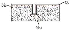
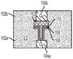
图1显示了本发明示例性的片上解耦电容100,其可适用于集成芯片。片上解耦电容器100包括两个铜布线104a和104b,其布置在层间介电材料层102内。层间介电材料层102将电容器100与外部的电路和元件电绝缘,以防止电流从电容器100泄漏。第一铜布线104a电耦合到底电极106,以及第二铜布线104b通过顶金属层112电耦合到顶电极110。底电极106和顶电极110可形成沟槽/叉头架构,其增加底电极106和顶电极110之间的表面积。隔离层108设置在底电极106和顶电极110之间,以使得顶电极110与底电极106电绝缘。在一个示例性的实施例中,隔离层108包括一个或多个碳纳米管,该一个或多个碳纳米管被设置为增加隔离层108的与电容相关的表面积并由此增加解耦电容器100的电容超过没有碳纳米管时的隔离层的电容。下面将结合图2和图3详细讨论的隔离层108。FIG. 1 shows an exemplary on-
图2显示了用于形成图1的片上解耦电容100的示例性隔离层108的碳纳米管202的示例性配置。出了底电极106以及由底电极106的表面之上的体积表示隔离层108。碳纳米管202沉积在底电极106上,并在示例性实施例中,形成碳纳米管202的网孔。该碳纳米管202可以在各种位置彼此接触,但由于它们的网孔设置或结构,可以其他方式形成它们之间的空间。一旦碳纳米管202沉积在底电极106上,在碳纳米管202上形成介电肤层(204,图3)。由于沉积的碳纳米管202的网孔状结构,可使用原子层沉积将介电肤层204沉积在碳纳米管202上。介电肤层204覆盖碳纳米管202的外表面以及底电极106的表面。一旦介电肤层204沉积在碳纳米管202上,金属涂层(206,图3)被沉积在介电肤层204上。使用是原子层沉积技术沉积金属涂层206,以形成基本上为圆柱形的外壳。FIG. 2 shows an exemplary configuration of
图3示出了在图1中的示例性形成的隔离层108的剖视图。示例性的碳纳米管202的表面上形成有介电肤层204。介电肤层204形成在碳纳米管202的外表面之上,并且可包括Al2O3、HfO2或其他合适的介电材料。介电肤层的厚度为约5纳米(nm)和20nm之间的范围内。在一个示例性实施例中,介电肤层204包括1纳米AlO2N3和8nm的HfO2。金属涂层206形成在介电肤层204的外表面上,并可能在介电层204周围形成同心结构。此外,金属涂层206可填充在碳纳米管/介质皮肤组件之间的间隙。在一个示例性实施例中,金属涂层206的厚度为约5nm到50nm之间的范围内。金属涂层206可能是氮化钽(TaN)或氮化钛(TiN)。在替代实施例中,金属层206可包括任何合适的导电金属,如铜,铝等。未被碳纳米管202、介电肤层204和金属涂层206的隔离层108的剩余部分被填充以合适的导电材料208(如铜,铝等)。形成隔离层108后,介电肤层204电隔离碳纳米管202与金属涂层206。因此,该电容被该碳纳米管202、碳纳米管202上的金属涂层206、以及碳纳米管202和金属涂层206之间的介电肤层204限定为纳米级。因此,介电肤层204的表面积与电容相关。FIG. 3 shows a cross-sectional view of the exemplary formed
图4-9示出了用于制造本发明的示例性的片上解耦电容器100的制造方法。图4示出了设置在层间介电材料的底介电层102a中形成的沟槽中的铜布线104a。在一个示例性实施例中,层间介电材料可被沉积在铜布线104a的顶表面上。也可以对底介电层102a进行化学机械抛光,以提供底介电层102a的光滑表面。也可以使用标准的光刻方法和反应性离子蚀刻,以露出铜布线104a的顶表面。4-9 illustrate a fabrication method for fabricating an exemplary on-chip decoupling
图5示出了图4中的底介电层102a和铜布线104a上形成的底电极106。可以由任何合适的导电金属形成底电极106,如铜或铝。在一个示例性实施例中,底电极106可使用原子层沉积(ALD)或化学气相沉积(CVD)进行沉积,并可能形成沟槽,该沟槽与在图4中形成的沟槽的形状相符。FIG. 5 shows the
图6示出了沉积在底电极106上的隔离层108。该隔离层108的沉积可分为数个阶段进行。如图2所示,在第一阶段中,一个或多个碳纳米管202沉积在底电极106上,从而附着在底电极106上。在第二阶段中,高k介电材料204沉积在碳纳米管202,以覆盖碳纳米管202和底电极106的表面。介电肤层204的厚度可以在从约5nm至约20nm的范围内。在一个示例性实施例中,介电肤层204可为约9nm的厚度,包括约1nm的AlO2N3以及约8nm的HfO2。高k介电材料204可使用原子层沉积或其他适合的沉积工艺进行沉积。在第三阶段中,金属涂层206被淀积以包围碳纳米管202和在其上形成介电肤层204,从而得到图3的示例性配置。金属涂层206可使用原子层沉积技术进行沉积,并且可以包括任何合适的导电金属,如铜、铝、氮化钽(TaN)等。金属涂层206可以是约5nm到50nm的厚度的TaN。如铜或铝的导电金属208,可被淀积以填充在隔离层108中。导电金属208可以是和金属涂层206相同的材料。在示范性实施例中,隔离层108的形状大致与底电极106一致,因此,可以保持通过底电极106设置的沟槽几何形状。FIG. 6 shows the
图7示出了沉积在隔离层108上的顶电极110和顶金属层112。可以使用原子层沉积或化学气相沉积法,或其它合适的方法用来沉积顶电极110。沉积顶电极110,以填充由底电极106和分离层108形成的沟槽。在一个示例性实施例中,顶电极110是金属涂层206相同的材料。因此,沉积顶电极110可出现在和沉积金属涂层206相同的步骤中。因此,顶电极110电耦合到隔离层108的金属涂层206,而底电极106电耦合到隔离层108中的碳纳米管202。顶电极110可以包括任何合适的导电金属,如铜铝、氮化钽、氮化钛等。顶金属层在完成顶电极沉积步骤之后在顶电极110上沉积。顶金属层112可以包括任何合适的导电金属,如铜铝、氮化钽、氮化钛等。FIG. 7 shows
图8示出了解耦电容器的电容单元的蚀刻表面。蚀刻工艺去除了远离沟槽区的底电极106、分离层108、顶电极110和顶金属层112的部分。使用标准光刻方法和反应性离子蚀刻,露出底的介电层102a的顶表面以形成蚀刻表面。FIG. 8 shows etched surfaces of capacitive cells of a decoupling capacitor. The etching process removes portions of the
图9示出了在图8中形成的电容单元的顶表面上沉积的层间介电材料的顶介电层102b。层间介电材料可被沉积在顶金属层112的顶表面上,以形成顶介电层102b。对所淀积的层间介电材料进行化学机械抛光,以提供顶介电层102b的光滑表面。使用标准的光刻方法和反应性离子蚀刻,露出顶金属层112的顶表面。顶介电层102b和底介电层102a一起形成图1中所示的层间介电材料层102。FIG. 9 shows a
图10示出了完整的片上解耦电容器。铜布线104b形成在图9中的沟槽中,以形成完整的解耦电容器。在一个示例性实施例中,铜布线104b可以由铜沉积和化学机械抛光形成。完整的电容器包括顶电极110、底电极106和分离层108。在隔离层中,通过金属涂层206、碳纳米管202和介电肤层204形成电容。因此,决定电容器的电容的面积与隔离层108中的介电肤层204的表面积相关。此电容面积大于未采用碳纳米管202的隔离层108提供的电容面积。因此,分离层108中的碳纳米管202的存在与在分离层108中没有碳纳米管时相比增加了电容器的电容。Figure 10 shows the complete on-chip decoupling capacitor.
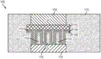
图11示出了单一的解耦电容器,其包括多个沟槽。蚀刻层间介电材料层1115,以在铜布线1101上形成若干沟槽。使用图4-10中所示的方法,在铜布线1101上分别形成底电极1106、隔离层1108、顶部电极1110、顶金属层1112和顶铜布线1102。解耦电容1100的每个沟槽都增加了电容器的表面积,从而增加解耦电容器1110的电容。虽然本文所公开的示例性的解耦电容器(即,图1和图11中的电容器)形成在层间介电材料中,在替代实施例中,电容器可以被形成在其他合适的材料中,例如硅。Figure 11 shows a single decoupling capacitor comprising multiple trenches. The interlayer
尽管对于解耦电容器使用术语“顶”和“底”描述解耦电容器的分层结构,但可以理解的是,这些术语仅用于说明目的,并且解耦电容器也可沿任何选择的方向定向。Although the terms "top" and "bottom" are used for the decoupling capacitors to describe the layered structure of the decoupling capacitors, it is understood that these terms are used for illustration purposes only and that the decoupling capacitors may be oriented in any chosen direction.
这里使用的术语仅用于用于描述特定实施例,而不旨在限制本发明的范围。如本文所用,单数形式“一个”、“这个”、“该”也可包括复数形式,除非上下文清楚地另有指示。进一步地,术语“包括”和/或“包含”在本说明书中使用时,指定所述的特征、整数(integer)、步骤、操作、元件和/或组件的存在,但不排除存在或增加其它特征、整数、步骤、操作、元素成分和/或它们的组。The terminology used herein is for describing particular embodiments only and is not intended to limit the scope of the present invention. As used herein, the singular forms "a", "the", and "the" may also include plural forms unless the context clearly dictates otherwise. Further, when the terms "comprising" and/or "comprising" are used in this specification, they specify the existence of the described features, integers, steps, operations, elements and/or components, but do not exclude the existence or addition of other Features, integers, steps, operations, constituents, and/or groups thereof.
在下面的权利要求中,相应的结构、材料、方式和所有装置或步骤加功能元件的替换物,也可包括与特别要求保护的其他要求保护的元件结合而实施功能的任何结构、材料或作用。本发明的说明书仅以描述的目的描述了本发明,但并非旨在穷举或限制本发明到所公开的形式。在本技术领域的普通技术人员不脱离本发明的范围和精神的情况下,许多修改和变化是显而易见的。实施例的选择和描述是为了最好地解释本发明的原理和实际应用,并使其他在本技术领域的普通技术人员能够理解本发明的具有适合于预期的特定用途的各种修改的各种实施例。In the following claims, the corresponding structures, materials, methods and all means or step plus function element replacements may also include any structure, material or action that performs the function in combination with other claimed elements that are specifically claimed . The description of the present invention has described the invention for purposes of illustration only, but is not intended to be exhaustive or to limit the invention to the form disclosed. Many modifications and variations will be apparent to those of ordinary skill in the art without departing from the scope and spirit of this invention. The embodiment was chosen and described in order to best explain the principles of the invention and the practical application, and to enable others skilled in the art to understand the invention for various modifications as are suited to the particular use contemplated. Example.
流程图只是一个示例。在不脱离本发明核心的情况下,本图或其中所述的步骤(或操作)可能有多种变化。例如,步骤可以不同的顺序执行,或者步骤可以被添加、删除或修改。所有这些变化都是所要求保护的本发明的一部分。The flowchart is just an example. There may be many variations to this diagram or the steps (or operations) described therein without departing from the spirit of the invention. For example, steps may be performed in a different order, or steps may be added, deleted or modified. All of these variations are a part of the claimed invention.
虽然已经描述了本发明的优选实施例,但可以理解的是,对本领域技术人员来说,无论是现在还是将来,可能在权利要求的范围内进行各种改进和增强。这些权利要求应解释保持对首次描述的本发明的适当保护。While the preferred embodiment of the present invention has been described, it will be understood that various improvements and enhancements may be made by those skilled in the art, both now and in the future, within the scope of the claims. These claims should be construed to maintain the proper protection for the invention first described.
Claims (40)
Translated fromChineseApplications Claiming Priority (2)
| Application Number | Priority Date | Filing Date | Title |
|---|---|---|---|
| US13/690,593US8766345B2 (en) | 2012-11-30 | 2012-11-30 | Area-efficient capacitor using carbon nanotubes |
| US13/690,593 | 2012-11-30 |
Publications (1)
| Publication Number | Publication Date |
|---|---|
| CN103855150Atrue CN103855150A (en) | 2014-06-11 |
Family
ID=50824650
Family Applications (1)
| Application Number | Title | Priority Date | Filing Date |
|---|---|---|---|
| CN201310594462.6APendingCN103855150A (en) | 2012-11-30 | 2013-11-21 | On-chip decoupling capacitor, integrated chip, and method of manufacturing same |
Country Status (2)
| Country | Link |
|---|---|
| US (2) | US8766345B2 (en) |
| CN (1) | CN103855150A (en) |
Cited By (1)
| Publication number | Priority date | Publication date | Assignee | Title |
|---|---|---|---|---|
| CN110534505A (en)* | 2019-08-29 | 2019-12-03 | 华中科技大学 | A kind of three-dimensional ferroelectric capacitor device, preparation method and ferroelectric memory |
Families Citing this family (12)
| Publication number | Priority date | Publication date | Assignee | Title |
|---|---|---|---|---|
| US9857328B2 (en) | 2014-12-18 | 2018-01-02 | Agilome, Inc. | Chemically-sensitive field effect transistors, systems and methods for manufacturing and using the same |
| CA2971589C (en) | 2014-12-18 | 2021-09-28 | Edico Genome Corporation | Chemically-sensitive field effect transistor |
| US9859394B2 (en) | 2014-12-18 | 2018-01-02 | Agilome, Inc. | Graphene FET devices, systems, and methods of using the same for sequencing nucleic acids |
| US9618474B2 (en) | 2014-12-18 | 2017-04-11 | Edico Genome, Inc. | Graphene FET devices, systems, and methods of using the same for sequencing nucleic acids |
| US10020300B2 (en) | 2014-12-18 | 2018-07-10 | Agilome, Inc. | Graphene FET devices, systems, and methods of using the same for sequencing nucleic acids |
| US10006910B2 (en) | 2014-12-18 | 2018-06-26 | Agilome, Inc. | Chemically-sensitive field effect transistors, systems, and methods for manufacturing and using the same |
| US9607943B2 (en) | 2015-06-11 | 2017-03-28 | International Business Machines Corporation | Capacitors |
| US10811539B2 (en) | 2016-05-16 | 2020-10-20 | Nanomedical Diagnostics, Inc. | Graphene FET devices, systems, and methods of using the same for sequencing nucleic acids |
| US11837534B2 (en)* | 2017-12-29 | 2023-12-05 | Intel Corporation | Substrate with variable height conductive and dielectric elements |
| US11264388B2 (en)* | 2020-05-18 | 2022-03-01 | Micron Technology, Inc. | Microelectronic devices including decoupling capacitors, and related apparatuses, electronic systems, and methods |
| KR20220056668A (en) | 2020-10-28 | 2022-05-06 | 삼성전자주식회사 | integrated circuit semiconductor device |
| KR20220070145A (en)* | 2020-11-20 | 2022-05-30 | 삼성전자주식회사 | semiconductor package |
Citations (11)
| Publication number | Priority date | Publication date | Assignee | Title |
|---|---|---|---|---|
| US20040131774A1 (en)* | 2002-09-20 | 2004-07-08 | Kellar Scot A. | Ultra-high capacitance device based on nanostructures |
| US20040188738A1 (en)* | 2002-03-06 | 2004-09-30 | Micron Technology, Inc. | Nanotube semiconductor devices and methods for making the same |
| US20040262637A1 (en)* | 2003-05-27 | 2004-12-30 | Infineon Technologies Ag | Memory device for storing electrical charge and method for fabricating the same |
| US20050064657A1 (en)* | 2002-03-28 | 2005-03-24 | Naoyuki Miyazawa | Interdigital capacitor and method for adjusting the same |
| US20050101099A1 (en)* | 2001-09-12 | 2005-05-12 | Kim Sarah E. | Method and device for on-chip decoupling capacitor using nanostructures as bottom electrode |
| US20060214262A1 (en)* | 2005-03-24 | 2006-09-28 | Intel Corporation | Capacitor with carbon nanotubes |
| CN101097889A (en)* | 2006-06-29 | 2008-01-02 | 海力士半导体有限公司 | Capacitor for memory device and method for forming the same |
| US20080239620A1 (en)* | 2007-03-30 | 2008-10-02 | Yongki Min | Carbon nanotube coated capacitor electrodes |
| CN101290835A (en)* | 2007-04-16 | 2008-10-22 | 韩国科学技术研究院 | A kind of electrode of supercapacitor and its manufacturing method |
| CN101438360A (en)* | 2004-11-24 | 2009-05-20 | 加利福尼亚大学董事会 | High power density supercapacitors with carbon nanotube electrodes |
| US8405189B1 (en)* | 2010-02-08 | 2013-03-26 | Lockheed Martin Corporation | Carbon nanotube (CNT) capacitors and devices integrated with CNT capacitors |
Family Cites Families (2)
| Publication number | Priority date | Publication date | Assignee | Title |
|---|---|---|---|---|
| US7767537B2 (en) | 2007-10-17 | 2010-08-03 | International Business Machines Corporation | Simplified method of fabricating isolated and merged trench capacitors |
| US8222104B2 (en) | 2009-07-27 | 2012-07-17 | International Business Machines Corporation | Three dimensional integrated deep trench decoupling capacitors |
- 2012
- 2012-11-30USUS13/690,593patent/US8766345B2/ennot_activeExpired - Fee Related
- 2013
- 2013-08-19USUS13/970,081patent/US8765547B2/ennot_activeExpired - Fee Related
- 2013-11-21CNCN201310594462.6Apatent/CN103855150A/enactivePending
Patent Citations (13)
| Publication number | Priority date | Publication date | Assignee | Title |
|---|---|---|---|---|
| US20050101099A1 (en)* | 2001-09-12 | 2005-05-12 | Kim Sarah E. | Method and device for on-chip decoupling capacitor using nanostructures as bottom electrode |
| US20040188738A1 (en)* | 2002-03-06 | 2004-09-30 | Micron Technology, Inc. | Nanotube semiconductor devices and methods for making the same |
| US20050064657A1 (en)* | 2002-03-28 | 2005-03-24 | Naoyuki Miyazawa | Interdigital capacitor and method for adjusting the same |
| US20050194628A1 (en)* | 2002-09-20 | 2005-09-08 | Kellar Scot A. | Capacitor with conducting nanostructure |
| US20040131774A1 (en)* | 2002-09-20 | 2004-07-08 | Kellar Scot A. | Ultra-high capacitance device based on nanostructures |
| US20040262637A1 (en)* | 2003-05-27 | 2004-12-30 | Infineon Technologies Ag | Memory device for storing electrical charge and method for fabricating the same |
| CN101438360A (en)* | 2004-11-24 | 2009-05-20 | 加利福尼亚大学董事会 | High power density supercapacitors with carbon nanotube electrodes |
| US20060214262A1 (en)* | 2005-03-24 | 2006-09-28 | Intel Corporation | Capacitor with carbon nanotubes |
| CN101097889A (en)* | 2006-06-29 | 2008-01-02 | 海力士半导体有限公司 | Capacitor for memory device and method for forming the same |
| US20080239620A1 (en)* | 2007-03-30 | 2008-10-02 | Yongki Min | Carbon nanotube coated capacitor electrodes |
| US20100177475A1 (en)* | 2007-03-30 | 2010-07-15 | Yongki Min | Carbon nanotube coated capacitor electrodes |
| CN101290835A (en)* | 2007-04-16 | 2008-10-22 | 韩国科学技术研究院 | A kind of electrode of supercapacitor and its manufacturing method |
| US8405189B1 (en)* | 2010-02-08 | 2013-03-26 | Lockheed Martin Corporation | Carbon nanotube (CNT) capacitors and devices integrated with CNT capacitors |
Cited By (1)
| Publication number | Priority date | Publication date | Assignee | Title |
|---|---|---|---|---|
| CN110534505A (en)* | 2019-08-29 | 2019-12-03 | 华中科技大学 | A kind of three-dimensional ferroelectric capacitor device, preparation method and ferroelectric memory |
Also Published As
| Publication number | Publication date |
|---|---|
| US20140154858A1 (en) | 2014-06-05 |
| US8765547B2 (en) | 2014-07-01 |
| US8766345B2 (en) | 2014-07-01 |
| US20140151847A1 (en) | 2014-06-05 |
Similar Documents
| Publication | Publication Date | Title |
|---|---|---|
| CN103855150A (en) | On-chip decoupling capacitor, integrated chip, and method of manufacturing same | |
| JP6046282B2 (en) | Metal insulator metal capacitor structure | |
| CN105706234B (en) | Structure with improved capacitor | |
| US8405135B2 (en) | 3D via capacitor with a floating conductive plate for improved reliability | |
| CN102569250B (en) | High-density capacitor and electrode leading-out method thereof | |
| US7897454B2 (en) | Metal-insulator-metal capacitor and fabrication method thereof | |
| US7821813B2 (en) | Nanowire memory device and method of manufacturing the same | |
| KR100873542B1 (en) | High Density Synthetic MIM Capacitors with Low Voltage Dependence in Semiconductor Dies | |
| US9337188B2 (en) | Metal-insulator-metal capacitor structure | |
| CN102655176B (en) | Capacitor with nano thread structure and preparation method thereof | |
| CN101996270A (en) | Method of designing semiconductor device and method of manufacturing the same | |
| JP2018107227A (en) | SEMICONDUCTOR DEVICE, SEMICONDUCTOR DEVICE MANUFACTURING METHOD, AND SOLID-STATE IMAGING ELEMENT | |
| CN116458282A (en) | Four-layer high-K for metal-insulator-metal capacitors | |
| CN111199956A (en) | A semiconductor device and method of forming the same | |
| US9142607B2 (en) | Metal-insulator-metal capacitor | |
| CN113130444A (en) | Semiconductor structure and forming method thereof | |
| CN115472433A (en) | High-density capacitive devices with well-defined insulating regions | |
| JP2018037626A (en) | Semiconductor device and semiconductor device manufacturing method | |
| CN108123040B (en) | MIM capacitor and its manufacturing method | |
| CN104752606B (en) | The forming method of resistance-type memory | |
| JP7713636B2 (en) | Capacitor, electric circuit, circuit board, device, and method for manufacturing capacitor | |
| CN103594525B (en) | A kind of semiconductor capacitor | |
| JP2011166032A (en) | Semiconductor device and method of manufacturing the same | |
| CN120388963A (en) | Metal-insulator-metal capacitor structure and manufacturing method thereof | |
| CN117116919A (en) | Semiconductor structures and methods of forming them |
Legal Events
| Date | Code | Title | Description |
|---|---|---|---|
| C06 | Publication | ||
| PB01 | Publication | ||
| C10 | Entry into substantive examination | ||
| SE01 | Entry into force of request for substantive examination | ||
| RJ01 | Rejection of invention patent application after publication | Application publication date:20140611 | |
| RJ01 | Rejection of invention patent application after publication |