CN103854699A - Nonvolatile memory, operating method thereof and calculation device - Google Patents
Nonvolatile memory, operating method thereof and calculation deviceDownload PDFInfo
- Publication number
- CN103854699A CN103854699ACN201310606617.3ACN201310606617ACN103854699ACN 103854699 ACN103854699 ACN 103854699ACN 201310606617 ACN201310606617 ACN 201310606617ACN 103854699 ACN103854699 ACN 103854699A
- Authority
- CN
- China
- Prior art keywords
- memory
- mode
- read
- write
- bank
- Prior art date
- Legal status (The legal status is an assumption and is not a legal conclusion. Google has not performed a legal analysis and makes no representation as to the accuracy of the status listed.)
- Granted
Links
Images


Classifications
- G—PHYSICS
- G11—INFORMATION STORAGE
- G11C—STATIC STORES
- G11C16/00—Erasable programmable read-only memories
- G11C16/02—Erasable programmable read-only memories electrically programmable
- G11C16/06—Auxiliary circuits, e.g. for writing into memory
- G—PHYSICS
- G11—INFORMATION STORAGE
- G11C—STATIC STORES
- G11C7/00—Arrangements for writing information into, or reading information out from, a digital store
- G11C7/10—Input/output [I/O] data interface arrangements, e.g. I/O data control circuits, I/O data buffers
- G11C7/1015—Read-write modes for single port memories, i.e. having either a random port or a serial port
- G11C7/1045—Read-write mode select circuits
- G—PHYSICS
- G11—INFORMATION STORAGE
- G11C—STATIC STORES
- G11C11/00—Digital stores characterised by the use of particular electric or magnetic storage elements; Storage elements therefor
- G11C11/02—Digital stores characterised by the use of particular electric or magnetic storage elements; Storage elements therefor using magnetic elements
- G11C11/16—Digital stores characterised by the use of particular electric or magnetic storage elements; Storage elements therefor using magnetic elements using elements in which the storage effect is based on magnetic spin effect
- G11C11/165—Auxiliary circuits
- G11C11/1653—Address circuits or decoders
- G—PHYSICS
- G11—INFORMATION STORAGE
- G11C—STATIC STORES
- G11C11/00—Digital stores characterised by the use of particular electric or magnetic storage elements; Storage elements therefor
- G11C11/02—Digital stores characterised by the use of particular electric or magnetic storage elements; Storage elements therefor using magnetic elements
- G11C11/16—Digital stores characterised by the use of particular electric or magnetic storage elements; Storage elements therefor using magnetic elements using elements in which the storage effect is based on magnetic spin effect
- G11C11/165—Auxiliary circuits
- G11C11/1673—Reading or sensing circuits or methods
- G—PHYSICS
- G11—INFORMATION STORAGE
- G11C—STATIC STORES
- G11C11/00—Digital stores characterised by the use of particular electric or magnetic storage elements; Storage elements therefor
- G11C11/02—Digital stores characterised by the use of particular electric or magnetic storage elements; Storage elements therefor using magnetic elements
- G11C11/16—Digital stores characterised by the use of particular electric or magnetic storage elements; Storage elements therefor using magnetic elements using elements in which the storage effect is based on magnetic spin effect
- G11C11/165—Auxiliary circuits
- G11C11/1675—Writing or programming circuits or methods
- G—PHYSICS
- G11—INFORMATION STORAGE
- G11C—STATIC STORES
- G11C7/00—Arrangements for writing information into, or reading information out from, a digital store
- G11C7/10—Input/output [I/O] data interface arrangements, e.g. I/O data control circuits, I/O data buffers
- G—PHYSICS
- G11—INFORMATION STORAGE
- G11C—STATIC STORES
- G11C7/00—Arrangements for writing information into, or reading information out from, a digital store
- G11C7/10—Input/output [I/O] data interface arrangements, e.g. I/O data control circuits, I/O data buffers
- G11C7/1078—Data input circuits, e.g. write amplifiers, data input buffers, data input registers, data input level conversion circuits
- G11C7/109—Control signal input circuits
- G—PHYSICS
- G11—INFORMATION STORAGE
- G11C—STATIC STORES
- G11C7/00—Arrangements for writing information into, or reading information out from, a digital store
- G11C7/22—Read-write [R-W] timing or clocking circuits; Read-write [R-W] control signal generators or management
- G11C7/222—Clock generating, synchronizing or distributing circuits within memory device
- G—PHYSICS
- G11—INFORMATION STORAGE
- G11C—STATIC STORES
- G11C8/00—Arrangements for selecting an address in a digital store
- G11C8/12—Group selection circuits, e.g. for memory block selection, chip selection, array selection
Landscapes
- Engineering & Computer Science (AREA)
- Computer Hardware Design (AREA)
- Microelectronics & Electronic Packaging (AREA)
- Read Only Memory (AREA)
- Techniques For Improving Reliability Of Storages (AREA)
- Storage Device Security (AREA)
Abstract
Translated fromChineseDescription
Translated fromChinese要求于2012年11月29日提交到韩国知识产权局的第10-2012-0137079号韩国专利申请的优先权,该韩国专利申请的全部内容通过引用合并与此。Priority is claimed from Korean Patent Application No. 10-2012-0137079 filed with the Korean Intellectual Property Office on November 29, 2012, the entire contents of which are hereby incorporated by reference.
技术领域technical field
在此描述的本发明的构思的实施例涉及半导体存储器,更具体地讲,涉及非易失性存储器和非易失性存储器的操作方法。Embodiments of the inventive concepts described herein relate to semiconductor memories, and more particularly, to nonvolatile memories and methods of operating the nonvolatile memories.
背景技术Background technique
使用诸如硅(Si)、锗(Ge)、砷化镓(GaAs)、磷化铟(InP)等半导体材料来制造半导体存储器装置。半导体存储器装置通常被分类为易失性存储器装置和非易失性存储器装置。Semiconductor memory devices are fabricated using semiconductor materials such as silicon (Si), germanium (Ge), gallium arsenide (GaAs), indium phosphide (InP), and the like. Semiconductor memory devices are generally classified into volatile memory devices and nonvolatile memory devices.
易失性存储器装置在断电时失去存储的内容。易失性存储器装置包括随机存取存储器(RAM)、静态RAM(SRAM)、动态RAM(DRAM)、同步DRAM(SDRAM)等。非易失性存储器装置甚至在断电时也保留存储的内容。非易失性存储器装置包括只读存储器(ROM)、可编程ROM(PROM)、电可编程ROM(EPROM)、电可擦除可编程ROM(EEPROM)、闪速存储器、相变RAM(PRAM)、磁RAM(MRAM)、电阻式RAM(RRAM)、铁电RAM(FRAM)等。特别地,通常快速地执行、消耗较少的电力并且具有良好的非易失性特性的MRAM会是下一代存储器。Volatile memory devices lose their stored content when powered off. Volatile memory devices include Random Access Memory (RAM), Static RAM (SRAM), Dynamic RAM (DRAM), Synchronous DRAM (SDRAM), and others. Non-volatile memory devices retain stored content even when powered off. Non-volatile memory devices include read-only memory (ROM), programmable ROM (PROM), electrically programmable ROM (EPROM), electrically erasable programmable ROM (EEPROM), flash memory, phase change RAM (PRAM) , Magnetic RAM (MRAM), Resistive RAM (RRAM), Ferroelectric RAM (FRAM), etc. In particular, MRAM, which generally performs fast, consumes less power, and has good non-volatile characteristics, will be the next generation of memory.
发明内容Contents of the invention
本发明构思的一方面提供了一种非易失性存储器,该非易失性存储器包括多个存储体(bank)、逻辑控制器和多个读写(RW)电路。每一个存储体包括多个存储器单元。逻辑控制器包括分别对应于所述多个存储体的多个存储单元,且被构造为基于存储在各个存储单元中的模式信息来将写使能信号和读使能信号输出给各个存储体。RW电路分别与存储体连接,且被构造为响应于各个存储体的写使能信号和读使能信号来独立地启用或禁用各个存储体的写操作和读操作。在模式信息被存储在各个存储单元之后的初始状态中,无论在各个存储单元中存储的模式信息如何,逻辑控制器都激活各个存储体的写使能信号和读使能信号。An aspect of the inventive concept provides a nonvolatile memory including a plurality of banks, a logic controller, and a plurality of read and write (RW) circuits. Each bank includes a plurality of memory cells. The logic controller includes a plurality of memory units respectively corresponding to the plurality of memory banks, and is configured to output a write enable signal and a read enable signal to each memory bank based on mode information stored in each memory unit. The RW circuits are respectively connected to the memory banks, and are configured to independently enable or disable the write operation and the read operation of the respective memory banks in response to the write enable signal and the read enable signal of the respective memory banks. In an initial state after mode information is stored in each memory cell, the logic controller activates a write enable signal and a read enable signal of each bank regardless of the mode information stored in each memory cell.
在示意性实施例中,在每一个存储单元中存储的模式信息可以包括与读使能信号相关联的读位和与写使能信号相关联的写位。In an exemplary embodiment, the mode information stored in each memory cell may include a read bit associated with a read enable signal and a write bit associated with a write enable signal.
在示意性实施例中,每一个存储体可以被控制为根据读位和写位的值以随机存取模式、只读模式、安全模式和易失性模式中的一个模式操作。In an exemplary embodiment, each memory bank can be controlled to operate in one of a random access mode, a read-only mode, a secure mode, and a volatile mode according to the values of the read bit and the write bit.
在示意性实施例中,当存储在从多个存储单元中选择的存储单元中的模式信息指示只读模式时,逻辑控制器还被构造为当在与选择的存储单元对应的存储体中执行写操作之后在选择的存储单元中设置写标记。In an exemplary embodiment, when the mode information stored in the memory unit selected from the plurality of memory units indicates a read-only mode, the logic controller is further configured to, when executing in the memory bank corresponding to the selected memory unit A write flag is set in the selected memory cell after the write operation.
在示意性实施例中,逻辑控制器可以基于在选择的存储单元中存储的模式信息和设置的写标记来去激活供应给与选择的存储单元对应的RW电路的写使能信号。In an exemplary embodiment, the logic controller may deactivate the write enable signal supplied to the RW circuit corresponding to the selected memory cell based on the mode information stored in the selected memory cell and the set write flag.
在示意性实施例中,当存储在从多个存储单元中选择的存储单元中的模式信息指示易失性模式时,逻辑控制器还可以被构造为当在与选择的存储单元对应的存储体中执行写操作之后在选择的存储单元中设置重置标记。In an exemplary embodiment, when the mode information stored in a memory unit selected from a plurality of memory units indicates a volatile mode, the logic controller may be further configured to, when in the memory bank corresponding to the selected memory unit A reset flag is set in the selected memory cell after a write operation is performed in .
在示意性实施例中,当与选择的存储单元对应的存储体被擦除(erase)时,逻辑控制器还可以被构造为重置在选择的存储单元中设置的重置标记。In an exemplary embodiment, when the memory bank corresponding to the selected memory cell is erased, the logic controller may be further configured to reset a reset flag set in the selected memory cell.
在示意性实施例中,当执行断电时,响应于在选择的存储单元中存储的模式信息和设置的重置标记,逻辑控制器可以控制与选择的存储单元对应的RW电路,使得与选择的存储单元对应的存储体被擦除可重置选择的存储单元的重置标记。In an exemplary embodiment, when power-off is performed, in response to the mode information stored in the selected memory cell and the reset flag set, the logic controller may control the RW circuit corresponding to the selected memory cell such that the selected The memory bank corresponding to the memory unit is erased to reset the reset flag of the selected memory unit.
在示意性实施例中,当执行重启(re-boot)时,响应于设置的重置标记,逻辑控制器可以控制与选择的存储单元对应的RW电路使得与选定的存储单元相对应的存储体被擦除,并且可以重置选择的存储单元的设置的重置标记。In an exemplary embodiment, when performing a re-boot, the logic controller may control the RW circuit corresponding to the selected memory unit so that the memory corresponding to the selected memory unit responds to the set reset flag. The memory cell is erased, and the reset flag of the selected memory cell can be reset.
在示意性实施例中,当存储在从多个存储单元中选择的存储单元中的模式信息指示安全模式时,响应于存储在选择的存储单元中的模式信息,逻辑控制器可以在选择的存储单元中设置写标记,并且可以去激活供应给与选择的存储单元对应的RW电路的写使能信号,并且可以在执行与选择的存储单元对应的存储体的写操作之后设置写标记。In an exemplary embodiment, when the mode information stored in a storage unit selected from a plurality of storage units indicates a security mode, in response to the mode information stored in the selected storage unit, the logic controller may, in the selected storage unit A write flag is set in the cell, and a write enable signal supplied to the RW circuit corresponding to the selected memory cell may be deactivated, and the write flag may be set after performing a write operation of the bank corresponding to the selected memory cell.
在示意性实施例中,当存储在从多个存储单元中选择的存储单元中的模式信息指示安全模式时,逻辑控制器还可以在执行写操作之后的与选择的存储单元对应的存储体的读操作之后在选择的存储单元中设置读标记。In an exemplary embodiment, when the mode information stored in a storage unit selected from a plurality of storage units indicates a security mode, the logic controller may further perform a write operation on the storage bank corresponding to the selected storage unit. A read flag is set in the selected memory cell after the read operation.
在示意性实施例中,逻辑控制器可以基于选择的存储单元的模式信息和设置的读标记,来去激活供应给与选择的存储单元对应的RW电路的读使能信号。In an exemplary embodiment, the logic controller may deactivate the read enable signal supplied to the RW circuit corresponding to the selected memory cell based on the mode information of the selected memory cell and the set read flag.
在示意性实施例中,当执行启动(boot)时,逻辑控制器可以重置设置的读标记。In an exemplary embodiment, the logic controller may reset the set read flag when performing a boot.
本发明构思的另一个方面提供一种操作非易失性存储器的方法,所述非易失性存储器包括多个存储体。所述方法包括:将存储体分成至少两个组;基于对应的模式信息来确定所述至少两个组中的每一组的操作的模式,该模式信息指示在所述至少两个组中的每一组中是否允许读操作并且是否允许写操作。在决定所述至少两个组中的每一组的操作的模式之后的初始状态中,无论操作模式如何都允许所述至少两个组中的每一组的写操作和读操作。Another aspect of the inventive concept provides a method of operating a nonvolatile memory including a plurality of banks. The method includes: dividing memory banks into at least two groups; determining a mode of operation of each of the at least two groups based on corresponding mode information indicating the Whether read operations are allowed and whether write operations are allowed in each group. In an initial state after deciding the mode of operation of each of the at least two groups, the write operation and the read operation of each of the at least two groups are allowed regardless of the operation mode.
在示意性实施例中,确定操作的模式的步骤可以包括确定所述至少两个组中的至少一个组处于允许写操作和读操作的随机存取模式。In an exemplary embodiment, the step of determining the mode of operation may include determining that at least one of the at least two groups is in a random access mode allowing write operations and read operations.
在示意性实施例中,确定操作模式可以包括确定所述至少两个组中的至少一个组处于只读模式,其中,在所述只读模式中,执行一个写操作并且随后的写操作被禁止,以及允许读操作。In an exemplary embodiment, determining the mode of operation may include determining that at least one of the at least two groups is in a read-only mode, wherein in the read-only mode, one write operation is performed and subsequent write operations are inhibited , and read operations are allowed.
在示意性实施例中,确定操作的模式的步骤可以包括确定所述至少两个组中的至少一个组处于安全模式,其中,在所述安全模式中,在执行初始的写操作之后禁止写操作,以及在执行启动期间的读操作之后禁止读操作。In an exemplary embodiment, the step of determining the mode of operation may include determining that at least one of the at least two groups is in a safe mode, wherein in the safe mode, write operations are prohibited after an initial write operation is performed , and disable read operations after a read operation during startup.
在示意性实施例中,确定操作模式可以包括确定所述至少两个组中的至少一个组处于易失性模式,其中,在所述易失性模式中,所述至少一个组在断电或通电时被擦除。In an exemplary embodiment, determining the mode of operation may include determining that at least one of the at least two banks is in a volatile mode, wherein in the volatile mode, the at least one bank is powered off or Erased at power-up.
在示意性实施例中,所述方法还可以包括:改变至少一个存储体的操作模式;响应于操作模式的改变来擦除模式被改变的所述至少一个存储体。In an exemplary embodiment, the method may further include: changing an operation mode of at least one memory bank; and erasing the at least one memory bank whose mode is changed in response to the change of the operation mode.
在示意性实施例中,所述方法还可以包括:接收用于改变至少一个存储体的操作模式的改变请求;根据改变请求执行认证操作;在认证操作通过时允许根据改变请求的操作的模式的改变,并且在认证操作失败时拒绝改变请求。In an exemplary embodiment, the method may further include: receiving a change request for changing the operation mode of at least one memory bank; performing an authentication operation according to the change request; allowing the operation of the mode according to the change request when the authentication operation passes change, and reject the change request if the authentication operation fails.
本发明构思的另一方面提供了一种非易失性存储器,所述非易失性存储器包括:共享读写(RW)电路的多个存储器块,每一个存储器块包括多个存储器单元;逻辑控制器,包括分别对应于所述多个存储器块的多个存储单元,并且被构造为基于存储在各个存储单元中的操作模式信息来将写使能信号和读使能信号输出到各个存储器块。RW电路被构造为响应于各个存储器块的写使能信号和读使能信号来独立地启用或禁用各个存储器块的写操作和读操作。在操作模式信息被存储在各个存储单元之后的初始状态中,无论在各个存储单元中存储的操作模式信息如何,逻辑控制器都启用相应的存储器块的写使能信号和读使能信号。Another aspect of the inventive concept provides a non-volatile memory including: a plurality of memory blocks sharing a read-write (RW) circuit, each memory block including a plurality of memory cells; logic a controller including a plurality of storage units respectively corresponding to the plurality of memory blocks, and configured to output a write enable signal and a read enable signal to the respective memory blocks based on operation mode information stored in the respective storage units . The RW circuit is configured to independently enable or disable a write operation and a read operation of each memory block in response to a write enable signal and a read enable signal of each memory block. In an initial state after operation mode information is stored in each memory cell, the logic controller enables a write enable signal and a read enable signal of a corresponding memory block regardless of the operation mode information stored in each memory cell.
通过本发明构思的实施例,存储体可以被划分为多个组。存储体的组可以按照不同的操作模式操作。因此,可以提高操作性能并提供用户便利性。Through an embodiment of the inventive concept, a memory bank may be divided into a plurality of groups. Groups of memory banks can operate according to different modes of operation. Therefore, it is possible to improve operability and provide user convenience.
本发明构思的另一方面提供了一种计算系统,所述计算系统包括被构造为控制操作的模式的应用处理器和被构造为从应用处理器接收模式信息的非易失性存储器。该非易失性存储器包括:多个存储体,每一个存储体包括多个存储器单元;逻辑控制器,包括分别对应于所述多个存储体的多个存储单元,并且被构造为基于识别操作的模式的在各个的存储单元中存储的模式信息来激活和去激活被提供给相应的存储体的写使能信号和读使能信号;多个读写(RW)电路,该多个RW电路分别与多个存储体连接,并且被构造为响应于基于在各个存储单元中存储的对应的模式信息激活和去激活各个存储体的写使能信号和读使能信号来独立地启用或禁用各个存储体的写操作和读操作。Another aspect of the inventive concept provides a computing system including an application processor configured to control a mode of operation and a nonvolatile memory configured to receive mode information from the application processor. The nonvolatile memory includes: a plurality of memory banks, each of which includes a plurality of memory units; a logic controller including a plurality of memory units respectively corresponding to the plurality of memory banks, and configured to operate based on the identification The mode information stored in each memory unit of the mode activates and deactivates the write enable signal and read enable signal provided to the corresponding memory bank; a plurality of read and write (RW) circuits, the plurality of RW circuits Connected to a plurality of memory banks, respectively, and configured to independently enable or disable each memory bank in response to a write enable signal and a read enable signal for activating and deactivating each memory bank based on corresponding mode information stored in each memory unit. Write and read operations of memory banks.
附图说明Description of drawings
根据下面参照附图的描述,上述和其它的目的和特征将变得明显,在各个图中相同的附图标记始终表示相同的部件,除非另有说明,在附图中:The above and other objects and features will become apparent from the following description with reference to the accompanying drawings, in which the same reference numerals denote the same components throughout, unless otherwise specified, in the drawings:
图1是示意性地图示根据本发明构思的实施例的计算系统的框图;FIG. 1 is a block diagram schematically illustrating a computing system according to an embodiment of the inventive concept;
图2是示意性地图示根据本发明构思的实施例的操作非易失性存储器的方法的流程图;2 is a flowchart schematically illustrating a method of operating a nonvolatile memory according to an embodiment of the inventive concept;
图3是示意性地图示根据本发明构思的实施例的非易失性存储器的框图;3 is a block diagram schematically illustrating a nonvolatile memory according to an embodiment of the inventive concept;
图4是示意性地图示根据本发明构思的实施例的操作非易失性存储器的方法的流程图;4 is a flowchart schematically illustrating a method of operating a nonvolatile memory according to an embodiment of the inventive concept;
图5是示出根据本发明构思的实施例的存储体或者读写电路的操作模式的表;5 is a table illustrating operation modes of a memory bank or a read and write circuit according to an embodiment of the inventive concept;
图6是示意性地图示根据本发明构思的实施例的设置计算系统的模式的方法的流程图;6 is a flowchart schematically illustrating a method of setting a mode of a computing system according to an embodiment of the inventive concept;
图7是示意性地图示根据本发明构思的实施例的的方法的流程图,在该方法中,计算系统控制处于只读模式中的非易失性存储器的至少一个存储体;7 is a flowchart schematically illustrating a method according to an embodiment of the inventive concept, in which method a computing system controls at least one bank of a nonvolatile memory in a read-only mode;
图8是示意性地图示根据本发明构思的实施例的的方法的流程图,在该方法中,计算系统控制处于安全模式中的至少一个存储体;8 is a flowchart schematically illustrating a method according to an embodiment of the inventive concept, in which method, a computing system controls at least one memory bank in a safe mode;
图9是示意性地图示根据本发明构思的实施例的的方法的流程图,在该方法中,计算系统控制处于易失性模式中的至少一个存储体;FIG. 9 is a flowchart schematically illustrating a method according to an embodiment of the inventive concept, in which method a computing system controls at least one memory bank in a volatile mode;
图10是示意性地图示根据本发明构思的另一实施例的设置计算系统的模式的方法的流程图;10 is a flowchart schematically illustrating a method of setting a mode of a computing system according to another embodiment of the inventive concept;
图11是示意性地图示根据本发明构思的另一实施例的设置计算系统的模式的方法的流程图;11 is a flowchart schematically illustrating a method of setting a mode of a computing system according to another embodiment of the inventive concept;
图12是示意性地图示根据本发明构思的另一实施例的设置计算系统的模式的方法的流程图;12 is a flowchart schematically illustrating a method of setting a mode of a computing system according to another embodiment of the inventive concept;
图13是示意性地图示根据本发明构思的实施例的存储器系统的框图;以及13 is a block diagram schematically illustrating a memory system according to an embodiment of the inventive concept; and
图14是示意性地图示根据本发明构思的另一实施例的非易失性存储器的框图。FIG. 14 is a block diagram schematically illustrating a nonvolatile memory according to another embodiment of the inventive concept.
具体实施方式Detailed ways
将针对下面的详细描述和附图来详细地描述实施例。但是,本发明构思可以以各种不同的形式来实施,并且不应该被解释为只限于说明性实施例。确切地说,这些实施例作为例子被提供,使得本公开将是彻底的、完整的,并且,将向本领域的普通技术人员全面地传达本发明构思。Embodiments will be described in detail with respect to the following detailed description and accompanying drawings. However, the inventive concept may be embodied in various forms and should not be construed as limited to the illustrative embodiments. Rather, these embodiments are provided as examples so that this disclosure will be thorough, complete, and will fully convey the inventive concept to those skilled in the art.
因此,关于本发明构思的一些实施例,可能对已知的处理、元件和技术不进行描述。除非另有说明,在所有的附图和说明书中相同的附图标记表示相同的元件,因此,将不会重复描述。在附图中,为了清楚起见,可以对层和区域的尺寸和相对尺寸进行放大。Therefore, known processes, elements and techniques may not be described with respect to some embodiments of the inventive concepts. Unless otherwise specified, the same reference numerals denote the same elements throughout the drawings and the specification, and therefore, descriptions will not be repeated. In the drawings, the size and relative sizes of layers and regions may be exaggerated for clarity.
将会理解,虽然在本文中可以使用术语“第一”、“第二”、“第三”等来描述各种元件、组件、区域、层和/或部分,但是,这些元件、组件、区域、层和/或部分不应该受这些术语的限制。这些术语仅仅用来将一个元件、组件、区域、层或部分与另一个元件、组件、区域、层或部分进行区分。因此,在不脱离本发明构思的教导的情况下,下面讨论的第一元件、组件、区域、层或部分可以被称为第二元件、组件、区域、层或部分。It will be understood that although the terms "first", "second", "third", etc. may be used herein to describe various elements, components, regions, layers and/or sections, these elements, components, regions , layer and/or section should not be limited by these terms. These terms are only used to distinguish one element, component, region, layer or section from another element, component, region, layer or section. Thus, a first element, component, region, layer or section discussed below could be termed a second element, component, region, layer or section without departing from the teachings of the inventive concept.
为了容易描述,在本文中可以使用诸如“在……之下”、“在……下面”、“下部的”、“在……下方”、“在……上方”、“上部的”等空间相对术语来描述一个元件或特征与另一个元件或特征的关系,如图所示。将会理解,除了图中绘出的取向以外,空间相对术语旨在还涵盖装置在使用或操作中的不同的取向。例如,如果图中的装置被翻转,那么被描述为在其它的元件或特征的“下面”或“之下”或“下方”的元件将会被取向为在其它的元件或特征的“上面”。因此,示例性术语“在……下面”和“在……下方”可以涵盖“上面”和“下面”的两种取向。装置可以以另外的方式被取向(旋转90度或者以其它的取向),并且,相应地,解释本文中使用的空间相对描述符。另外,还将会理解,当一个层被提及为在两个层“之间”时,它可以是两个层之间的唯一层,或者,还可以存在一个或多个中间层。For ease of description, spaces such as "under", "beneath", "lower", "below", "above", "upper" may be used herein Relative terms are used to describe the relationship of one element or feature to another element or feature as shown in the figures. It will be understood that the spatially relative terms are intended to encompass different orientations of the device in use or operation in addition to the orientation depicted in the figures. For example, if the device in the figures is turned over, elements described as "below" or "beneath" or "beneath" other elements or features would then be oriented "above" the other elements or features . Thus, the exemplary terms "below" and "beneath" can encompass both an orientation of "above" and "beneath". A device may be otherwise oriented (rotated 90 degrees or at other orientations) and the spatially relative descriptors used herein interpreted accordingly. In addition, it will also be understood that when a layer is referred to as being "between" two layers, it can be the only layer between the two layers, or one or more intervening layers may also be present.
本文中使用的术语仅仅出于描述特定实施例的目的,并且不应当限制本发明构思。如本文中使用的,单数形式“一个”、“一种”和“该”应当也包括复数形式,除非上下文中明确地另有说明。将会进一步理解,术语“包括”和/或“包含”在本说明书中使用时指定所述的特征、整体、步骤、操作、元件和/或组件的存在,但是不排除一个或多个其它的特征、整体、步骤、操作、元件、组件和/或其集合的存在或添加。如本文中使用的,术语“和/或”包括相关列举项目中的一个或多个的所有的任何组合。此外,术语“示例性的”应当是指例子或实例。The terminology used herein is for the purpose of describing particular embodiments only and should not limit the inventive concept. As used herein, the singular forms "a", "an" and "the" shall also include the plural forms unless the context clearly dictates otherwise. It will be further understood that the terms "comprising" and/or "comprising" when used in this specification specify the presence of stated features, integers, steps, operations, elements and/or components, but do not exclude one or more other Presence or addition of features, integers, steps, operations, elements, components and/or collections thereof. As used herein, the term "and/or" includes any combination of one or more of the associated listed items. Furthermore, the term "exemplary" shall mean an example or instance.
将会理解,当一个元件或层被提到在另一个元件或层“上”,与另一个元件或层“连接”、“耦接”或者“相邻”时,它可以直接在另一个元件或层上,直接与另一个元件或层连接、耦接、或者相邻,或者,可以存在中间元件或层。与此形成对照的是,当一个元件被提到“直接在另一个元件或层上”,与另一个元件或层“直接连接”、“直接耦接”或“直接相邻”时,不存在中间元件或层。It will be understood that when an element or layer is referred to as being “on,” “connected to,” “coupled to,” or “adjacent” to another element or layer, it can be directly on the other element or layer. or layer, directly connected to, coupled to, or adjacent to another element or layer, or intervening elements or layers may be present. In contrast, when an element is referred to as being "directly on," "directly connected to," "directly coupled to," or "directly adjacent to" another element or layer, there is no Intermediate elements or layers.
除非另有定义,本文中使用的所有的术语(包括技术术语和科学技术)具有与本发明构思所属技术领域的普通技术人员所通常理解的含义相同的含义。将会进一步理解,诸如常用词典中定义的术语的术语应该被解释为具有与其在相关领域和/或本说明书的环境中的含义一致的含义,并且将不会被解释为理想化的或过于正式的意义,除非本文中另有明确的定义。Unless otherwise defined, all terms (including technical terms and scientific techniques) used herein have the same meaning as commonly understood by one of ordinary skill in the technical field to which this invention belongs. It will be further understood that terms such as those defined in commonly used dictionaries should be interpreted to have meanings consistent with their meanings in the relevant field and/or in the context of this specification, and will not be interpreted as idealized or overly formal unless otherwise expressly defined herein.
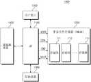
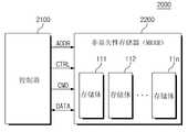
图1是示意性地示出根据本发明构思的实施例的计算系统1000的框图。例如,计算系统1000可以是移动多媒体装置。参照图1,计算系统1000包括应用处理器1100、非易失性存储器1200、存储装置1300、调制解调器1400和用户接口1500。FIG. 1 is a block diagram schematically illustrating a
应用处理器1100控制计算系统1000的整体操作并执行逻辑运算。例如,应用处理器1100可以由片上系统(SoC)形成。The
非易失性存储器1200可以用作计算系统1000的工作存储器。非易失性存储器1200可以包括各种类型的非易失性存储器,例如,磁RAM(MRAM)、相变RAM(PRAM)、电阻式RAM(RRAM)、铁电RAM(FRAM)等。在示出的示例中,假设非易失性存储器1200包括MRAM,但是本发明构思的实施例并不局限于此。The
非易失性存储器1200可以从应用处理器1100接收地址ADDR、控制信号CTRL和命令CMD。此外,非易失性存储器1200可以与应用处理器1100交换数据DATA。非易失性存储器1200包括多个存储体111至11n。存储体111至11n中的每一个可以包括能够独立地执行读、写或擦除的一组存储器单元。The
存储体111至11n可以被划分为多个组。例如,组可以被控制为在诸如随机存取模式、只读模式、安全模式和易失性模式的不同的操作模式中操作。组的操作模式可以由应用处理器110来控制。The
图1示出,非易失性存储器1200包括多个存储体111至11n的示例。但是,本发明构思的实施例并不局限于此。例如,非易失性存储器1200可以包括多个存储器块,其中,每一个存储器块包括多个存储器单元。存储器块可以是共享外围电路来执行读、写或擦除的存储器单元的集合。存储器块可能不会同时执行读、写或擦除。从这些存储器块选择的一个存储器块可执行读、写或擦除。在各种实施例中,存储体可以包括多个存储器块。FIG. 1 shows an example in which a
下面将针对非易失性存储器1200的存储体(例如,存储体111至11n)来描述本发明构思的实施例。例如,将描述通过诸如随机存取模式、只读模式、安全模式和易失性模式的各种操作模式控制的非易失性存储器1200的存储体。但是,本教导的精神和范围也可以被扩展到存储器块。例如,除了不同时执行读、写或擦除的事实以外,本发明构思的实施例可以被应用到非易失性存储器1200的存储器块。同样地,可以通过诸如随机存取模式、只读模式、安全模式和易失性模式等的各种操作模式控制非易失性存储器1200的存储器块。Embodiments of the inventive concept will be described below with respect to banks (eg,
存储装置1300可以用作用于计算系统的存储设备(storage)。存储设备可以长时间段地保留数据。存储装置1300可以包括各种类型的非易失性存储器,诸如,闪速存储器、硬盘驱动器(HDD)、MRAM、PRAM、RRAM、FRAM等。The
在示意性实施例中,非易失性存储器1200和存储装置1300可以被集成在组合的存储器中。存储器的第一部分可以用作非易失性存储器1200,并且存储器的第二部分可以用作存储装置1300。In an exemplary embodiment, the
调制解调器1400可以在应用处理器1100的控制下与外部装置执行有线或无线通信。调制解调器1400可以基于各种通信标准(诸,如WiFi、CDMA、GSM、LTE、Bluetooth、NFC等中的至少一个)进行通信。在示例性实施例中,调制解调器1400可以与应用处理器110一起构成片上系统。The
用户接口1500被构造为与外部装置(未示出)交换信号。例如,用户接口1500可以包括一个或多个用户输入接口,诸如,键盘、键区、按钮、触摸面板、触摸屏、触摸板、触摸球、相机、麦克风、陀螺仪传感器、振动传感器等。用户接口1500还可以包括一个或多个用户输出接口,例如,液晶显示器(LCD)、有机发光二极管(OLED)显示装置、有源矩阵OLED(AMOLED)显示装置、发光二极管(LED)、扬声器、电机等。The
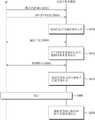
图2是示意性示出根据本发明构思的实施例的操作非易失性存储器1200的方法的流程图。参照图1和2,在操作S110中,多个存储体被划分为少两个组。在操作S120中,分别决定划分的组的读使能模式和写使能模式。可通过分别决定划分的组的读使能模式和写使能模式,来独立地控制划分的组的操作模式。FIG. 2 is a flowchart schematically illustrating a method of operating a
图3是示意性示出根据本发明构思的实施例的非易失性存储器1200的框图。参照图1和3,非易失性存储器1200包括多个存储体111至11n、多个读写(RW)电路121至12n和逻辑控制器130。FIG. 3 is a block diagram schematically illustrating a
存储体111至11n中的每一个可以包括多个存储器单元。例如,包括在存储体111至11n中的每一个的存储器单元可以是磁存储器单元。此外,在存储体111至11n中的每一个中,存储器单元可以按照三维结构堆叠。Each of the
RW电路121至12n分别与存储体111至11n连接。RW电路121至12n可以独立地执行对存储体111至11n的读、写和擦除。RW电路121至12n可以与应用处理器1100交换数据。例如,RW电路121至12n可以将从存储体111至11n读取的数据输出到应用处理器1100,并且将从应用处理器1100传输的数据分别写入到存储体111至11n。
图3示出RW电路121至12n被设置在对应的存储体111至11n的一侧的示例。但是,本发明构思的实施例并不局限于此。RW电路121至12n中的每一个可以包括用于选择对应的存储体中的存储器单元的行的行解码器和用于选择存储器单元的列的列解码器。FIG. 3 shows an example in which the
RW电路121至12n中的每一个被构造为从逻辑控制器130接收读使能信号RE和写使能信号WE。当读使能信号RE被激活时,与激活的读使能信号RE对应的RW电路121至12n在逻辑控制器130的控制下执行读操作。当读使能信号RE被去激活时,无论逻辑控制器130的试图控制如何,与去激活的读使能信号RE对应的RW电路121至12n不执行读操作。当写使能信号WE被激活时,与激活的写使能信号WE对应的RW电路121至12n在逻辑控制器130的控制下执行写操作。当写使能信号WE被去激活时,无论逻辑控制器130的试图控制如何,与去激活的写使能信号WE对应的RW电路121至12n都不执行写操作。Each of the
也就是说,读使能信号RE分别允许和禁止RW电路121至12n中的每一个的读操作,并且写使能信号WE分别允许和禁止RW电路121至12n中的每一个的写操作。That is, the read enable signal RE respectively enables and disables the read operation of each of the
逻辑控制器130被构造为控制非易失性存储器1200的整体操作。逻辑控制器130还被构造为响应于来自应用处理器1100的控制信号CTRL、命令CMD和地址ADDR来控制RW电路121至12n。The
在示出的实施例中,逻辑控制器130包括存储电路140。存储电路140包括分别对应于存储体111至11n和/或RW电路121至12n的存储单元S1至Sn。In the illustrated embodiment,
存储单元S1至Sn被构造为存储对应的存储体111至11n和/或RW电路121至12n的模式信息。模式信息可包括与读使能信号相关联的读位和与写使能信号相关联的写位。逻辑控制器130可以基于存储在存储单元S1至Sn中的模式信息,来激活或去激活读使能信号RE和写使能信号WE。也就是说,逻辑控制器130可以基于存储在存储单元S1至Sn中的模式信息,来控制存储体111至11n或RW电路121至12n的模式。The storage units S1 to Sn are configured to store mode information of the
在各种实施例中,存储单元S1至Sn可以存储非易失性模式信息。例如,存储单元S1至Sn可以是模式寄存器。逻辑控制器130被构造为响应于从应用处理器1100传输的特定命令而进入模式寄存器设置模式。在模式寄存器设置模式中,逻辑控制器130可以根据从应用处理器1100传输的信息(例如,ADDR、CTRL、CMD或DATA)在存储单元S1至Sn中存储模式信息。In various embodiments, the storage units S1 to Sn may store nonvolatile mode information. For example, the storage units S1 to Sn may be mode registers. The
在示意性实施例中,存储单元S1至Sn可以是熔丝。当存储单元S1至Sn由例如电熔丝形成时,它们可以存储与模式寄存器相同的模式信息。当存储单元S1至Sn由例如激光熔丝形成时,它们可以通过激光切割来存储模式信息。In exemplary embodiments, the memory cells S1 to Sn may be fuses. When the memory cells S1 to Sn are formed of, for example, electric fuses, they can store the same mode information as the mode register. When the memory cells S1 to Sn are formed of, for example, laser fuses, they can store mode information by laser cutting.
图4是示意性示出根据本发明构思的实施例的操作非易失性存储器1200的方法的流程图。图4示出在存储单元S1至Sn由模式寄存器形成时非易失性存储器1200操作的示例。FIG. 4 is a flowchart schematically illustrating a method of operating the
参照图1、3和4,在操作S210中,接收寄存器设置命令CMD。非易失性存储器1200的逻辑控制器130可以从应用处理器1100接收寄存器设置命令CMD。例如,逻辑控制器130可基于接收的寄存器设置命令CMD进入模式寄存器设置模式。Referring to FIGS. 1, 3 and 4, in operation S210, a register setting command CMD is received. The
在操作S220中,非易失性存储器1200接收地址和模式信息。逻辑控制器130可以接收来自应用处理器1100的存储体的地址和与对应于所接收到的地址的存储体相关联的模式信息。模式信息可以以地址、命令、控制信号或数据形式从应用处理器1100传输到非易失性存储器1200。当模式信息以数据形式被传输时,用于传输模式信息的单独的数据路径可以被设置在RW电路121至12n和逻辑控制器130之间。In operation S220, the
在操作S230中,逻辑控制器130根据接收到的地址在存储单元S1至Sn中存储模式信息。在操作S240中,逻辑控制器130响应于存储在存储单元S1至Sn中的模式信息来控制读使能信号RE和写使能信号WE。因此,逻辑控制器130可以激活或去激活分别与存储体111或11n或者RW电路121或12n相对应的读使能信号RE和写使能信号WE。In operation S230, the
图5是示出根据本发明构思的实施例的根据模式信息的存储体111或11n或者读写电路121或12n的操作模式的表。参照图1、4和5,模式信息包括写信息W和读信息R。写信息W指示对应的存储体或RW电路的写模式,并且读信息R指示对应的存储体或RW电路的读模式。读信息R和写信息W可分别对应于如上所述的与读使能信号相关联的读位和与写使能信号相关联的写位,但不限于此。FIG. 5 is a table illustrating an operation mode of the
参照图5中示出的示例,当写信息W和读信息R都具有第一值(例如,1)时,写使能信号WE和读使能信号RE被激活。于是,对应的存储体或RW电路被写使能和被读使能,由此响应于激活的写使能信号WE和读使能信号RE来执行写操作和读操作。因此,与存储有具有第一值的写信息W和具有第一值的读信息R的存储单元相对应的存储体或RW电路处于随机存取模式。Referring to the example shown in FIG. 5 , when both the write information W and the read information R have a first value (for example, 1), the write enable signal WE and the read enable signal RE are activated. Accordingly, the corresponding memory bank or RW circuit is write-enabled and read-enabled, thereby performing write and read operations in response to the activated write-enable signal WE and read-enable signal RE. Accordingly, the memory bank or RW circuit corresponding to the memory cell storing the write information W having the first value and the read information R having the first value is in the random access mode.
当写信息W具有第二值(例如,0)并且读信息R具有第一值时,写使能信号WE被初始地激活直到针对对应的存储体或RW电路执行写操作,并且然后该写使能信号WE被去激活。读使能信号RE被激活。于是,对应的存储体或RW电路被一次写使能,和读使能。因此,与存储有具有第二值的写信息W和具有第一值的读信息R的存储单元相对应的存储体或RW电路处于只读模式。When the write information W has a second value (for example, 0) and the read information R has a first value, the write enable signal WE is initially activated until a write operation is performed for the corresponding bank or RW circuit, and then the write enables The enable signal WE is deactivated. The read enable signal RE is activated. Then, the corresponding memory bank or RW circuit is enabled for writing once, and enabled for reading. Therefore, the memory bank or RW circuit corresponding to the memory cell storing the write information W having the second value and the read information R having the first value is in the read-only mode.
在示意性实施例中,与处于只读模式的存储体或RW电路相关联的存储单元还存储写标记作为附加模式信息。当在存储体或RW电路中初始地执行写操作时,设置存储单元的写标记,从而在写标记被重置之前禁止进一步的写操作。换句话说,当写标记处于重置状态中时,逻辑控制器130保持写使能信号WE处于激活状态,并且当写标记处于设置的状态时,逻辑控制器130去激活写使能信号WE。In an exemplary embodiment, memory cells associated with banks or RW circuits in read-only mode also store write flags as additional mode information. When a write operation is initially performed in a bank or RW circuit, the write flag of the memory cell is set, thereby inhibiting further write operations until the write flag is reset. In other words, when the write flag is in the reset state, the
再次参照图5,在写信息W和读信息R二者具有第二值时写使能信号WE被初始地激活直到针对对应的存储体或RW电路执行写操作,并且然后该使能信号WE被去激活。同样地,读使能信号RE被初始地激活直到(在计算系统1000的启动开始之后)执行读操作,并且然后该读使能信号RE被去激活。于是,对应的存储体或RW电路被一次写使能和一次读使能。因此,与存储有具有第二值的写信息W和具有第二值的读信息R的存储单元相对应的存储体或RW电路处于安全(或者,启动)模式。Referring again to FIG. 5 , the write enable signal WE is initially activated when both the write information W and the read information R have the second value until a write operation is performed for the corresponding memory bank or RW circuit, and then the enable signal WE is activated go activate. Likewise, the read enable signal RE is initially activated until (after booting of the
在示意性实施例中,与处于安全模式的存储体或RW电路相关联的存储单元还存储写标记和读标记作为附加模式信息。当最存储体或RW电路中初始地执行写操作时,存储单元的写标记被设置,从而在写标记被重置之前禁止进一步的写操作。换句话说,当写标记处于重置状态时,逻辑控制器130保持写使能信号WE处于激活状态,并且当写标记处于设置的状态时,逻辑控制器130去激活写使能信号WE。类似地,当在RW电路中初始地执行读操作时(在开机启动之后),存储单元的读标记被设置,从而在读标记被重置之前禁止进一步的读操作。换句话说,当读标记处于重置状态时,逻辑控制器130保持读使能信号RE处于激活状态,并且当读标记处于设置的状态时,逻辑控制器130去激活读使能信号RE。In an exemplary embodiment, memory cells associated with banks or RW circuits in secure mode also store write flags and read flags as additional mode information. When a write operation is initially performed in the most bank or RW circuit, the write flag of the memory cell is set, thereby inhibiting further write operations until the write flag is reset. In other words, when the write flag is in the reset state, the
最后,当写信息W具有第一值,且读信息R具有第二值时,写使能信号WE和读使能信号RE保持激活状态。于是,对应的存储体或RW电路是特殊读/写使能,并且在断电之前被重置。因此,与其中存储具有第一值的写信息W和具有第二值的读信息R的存储单元相对应的存储体或RW电路处于易失性模式。Finally, when the write information W has the first value and the read information R has the second value, the write enable signal WE and the read enable signal RE maintain an active state. The corresponding bank or RW circuit is then special read/write enabled and reset prior to power down. Accordingly, a bank or RW circuit corresponding to a memory cell in which write information W having a first value and read information R having a second value is stored is in a volatile mode.
在示意性实施例中,与处于易失性模式的存储体或RW电路相关联的存储单元还存储重置标记作为附加模式信息。当在存储体或RW电路中执行写操作时,对应的存储单元的重置标记被设置。当写入到存储体或RW电路中的所有的数据被擦除时,该重置标记被重置。当重置标记处于重置状态时,逻辑控制器130在断电或通电时控制存储体或RW电路,使得写入到存储体中的数据全部被擦除。In an exemplary embodiment, memory cells associated with banks or RW circuits in volatile mode also store reset flags as additional mode information. When a write operation is performed in a bank or RW circuit, the reset flag of the corresponding memory cell is set. The reset flag is reset when all data written into the bank or RW circuit is erased. When the reset flag is in the reset state, the
因此,一般地,在操作模式被决定之后,无论操作模式如何都允许初始的写操作和读操作。换句话说,在模式信息被存储到相应的存储单元之后的初始状态中,无论在相应的存储单元中存储的模式信息如何,逻辑控制器130都初始地激活相应的存储体或RW电路的写使能信号WE和读使能信号RE。Therefore, generally, after the operation mode is decided, the initial write operation and read operation are allowed regardless of the operation mode. In other words, in the initial state after the mode information is stored in the corresponding memory unit, regardless of the mode information stored in the corresponding memory unit, the
图6是示意性示出根据本发明构思的实施例的设置计算系统1000的模式的方法的流程图。参照图1、3、5和6,在操作S310中,应用处理器1100将模式设置命令CMD发送给非易失性存储器1200。模式设置命令CMD可根据非易失性存储器1200的规格而被预先确定。在操作S320中,应用处理器1100将地址和模式信息发送给非易失性存储器1200。FIG. 6 is a flowchart schematically illustrating a method of setting a mode of the
在操作S330中,非易失性存储器1200在存储单元S1至Sn中存储模式信息。存储体111至11n或RW电路121至12n的操作的模式分别根据存储的模式信息而被决定。In operation S330, the
在操作S340中,应用处理器1100和非易失性存储器1200通过允许授权的存取并拒绝未经授权的存取,来相互通信。例如,当应用处理器1100请求在具有只读模式或安全模式的存储体中的写操作时,非易失性存储器1200可以拒绝该写请求。In operation S340, the
在示意性实施例中,应用处理器1100可以通过从应用处理器1100向非易失性存储器1200发送模式设置命令CMD,来改变对非易失性存储器1200的存储体111至11n设置的模式。In an exemplary embodiment, the
在示意性实施例中,非易失性存储器1200的存储体111至11n可以分别具有随机访问模式作为默认值。通过从应用处理器1100向非易失性存储器1200发送模式设置命令CMD,存储体111至11n的模式被设置为另一模式。在示意性实施例中,可以通过对BIOS的设置来执行对非易失性存储器1200的模式的改变。In an exemplary embodiment, the
图7是示意性示出计算系统1000控制非易失性存储器1200的具有只读模式的至少一个存储体的方法的流程图。参照图1、4、5和7,在操作S410中,应用处理器1100将模式设置命令CMD发送给非易失性存储器1200。在操作S420中,应用处理器1100将至少一个存储体的地址和只读模式信息发送给非易失性存储器1200。也就是说,应用处理器1100可以向非易失性存储器1200提供将以只读模式被控制的至少一个存储体的地址。如上面参照图5所讨论的,应用处理器1100可以向非易失性存储器1200提供具有第二值(例如,0)的写信息W和具有第一值(例如,1)的读信息R作为模式信息。FIG. 7 is a flowchart schematically illustrating a method for the
在操作S430中,非易失性存储器1200在与接收到的地址对应的存储单元中存储传输的只读模式信息。通过在存储单元中存储只读模式信息,可以以只读模式控制与接收到的地址对应的存储体或RW电路。In operation S430, the
在操作S440中,应用处理器1100将地址和只读模式数据发送给非易失性存储器1200。例如,应用处理器1100可将将以只读模式被控制的存储体的地址和将被写入到该存储体中的数据发送给非易失性存储器1200。The
在操作S450中,非易失性存储器1200在具有只读模式的存储体中写入传输的只读模式数据。在写入只读模式数据之后,非易失性存储器1200设置与写入有只读模式数据的存储体相对应的存储单元的写标记。如果写标记被设置,则非易失性存储器1200的逻辑控制器130去激活写使能信号WE。也就是说,对于写入有只读模式数据的存储体上的随后的写操作被禁止。In operation S450, the
在示意性实施例中,只读模式数据可以包括更新禁止数据,例如,计算系统1000的硬件信息、BIOS程序、计算系统1000的固有号等。如果只读模式数据被写入,则对于具有只读模式的存储体的写入被禁止。因此,可以无损耗地保留在具有只读模式的存储体中编程的数据。In an exemplary embodiment, the read-only mode data may include update prohibition data, for example, hardware information of the
在操作S460中,应用处理器1100和非易失性存储器1200通过允许对于具有只读模式的存储体的读操作并禁止对于具有只读模式的存储体的写操作,来相互通信。In operation S460, the
图8是示意性示出计算系统1000控制具有安全模式的至少一个存储体的方法的流程图。参照图1、4、5和8,在操作S510中,应用处理器1100将模式设置命令CMD发送给非易失性存储器1200。在操作S520中,应用处理器1100将地址和安全模式信息发送给非易失性存储器1200。应用处理器1100可以向非易失性存储器1200提供将以安全模式被控制的至少一个存储体的地址。如上面参照图5所讨论的,应用处理器1100可以向非易失性存储器1200提供具有第二值(例如,0)的写信息W和具有第二值的读信息R作为模式信息。FIG. 8 is a flowchart schematically illustrating a method for the
在操作S530中,非易失性存储器1200在与接收到的地址对应的存储单元中存储传输的安全模式信息。在操作S540中,应用处理器1100将地址和安全模式数据发送给非易失性存储器1200。例如,应用处理器1100可将将以安全模式被控制的存储体的地址和将被写入到该存储体中的数据发送给非易失性存储器1200。In operation S530, the
在操作S550中,非易失性存储器1200在与接收到的地址对应的存储体中写入接收到的安全模式数据,并且设置与写入有安全模式数据的存储体相关联的存储单元的写标记。如果写标记被设置,则非易失性存储器1200的逻辑控制器130可以去激活写使能信号WE。也就是说,对于写入有安全模式数据的存储体的随后的写操作被禁止。In operation S550, the
在示意性实施例中,安全模式数据可以包括与计算系统1000的启动相关联的信息。安全模式数据可以包括在计算系统1000启动时所需的安全信息、识别信息等。如果安全模式数据被写入,则对于具有安全模式的存储体的写入可被禁止。因此,可以无损耗地保留安全模式数据。In an illustrative embodiment, the security mode data may include information associated with the startup of
在操作S560中,执行重启。重启可以包括硬重置和软重置,其中,硬重置允许在去除计算系统1000的电力之后再次供电,软重置允许在保持计算系统1000的电力的情况下执行操作系统(OS)重启。无论何时执行重启,非易失性存储器1200重置与具有安全模式的存储体相关联的存储单元的读标记。在示意性实施例中,非易失性存储器1200可以通过检测从应用处理器1100传输的重置信号或者供应的电力的电平的增加,来重置读标记。In operation S560, a reboot is performed. Rebooting may include a hard reset, which allows power to be reapplied to the
在操作S570中,当在非易失性存储器1200处启动时,应用处理器1100请求读操作。应用处理器1100将具有安全模式的存储体的地址与读请求一起发送。In operation S570, when booting at the
在操作S580中,非易失性存储器1200根据读请求读取在具有安全模式的存储体中存储的安全模式数据。如果读操作被执行,则逻辑控制器130设置与具有安全模式的存储体相关联的存储单元的读标记。如果读标记被设置,则逻辑控制器130可以去激活读使能信号RE。也就是说对于具有安全模式的存储体的随后的读操作被禁止。In operation S580, the
在操作S590中,应用处理器1100和非易失性存储器1200通过禁止对于具有安全模式的存储体的RW操作,来相互通信。In operation S590, the
如果安全模式数据在启动时被读取,则对于具有安全模式的存储体的随后的访问可被拒绝。因此,可以确保对于具有安全模式的存储体中存储的安全模式数据的安全。If secure mode data is read at boot time, subsequent access to a bank with secure mode may be denied. Therefore, security for security mode data stored in a bank having a security mode can be ensured.
图9是示意性示出计算系统1000控制具有易失性模式的至少一个存储体的方法的流程图。参照图1、4、5和9,在操作S610中,应用处理器1100将模式设置命令CMD发送给非易失性存储器1200。FIG. 9 is a flowchart schematically illustrating a method of the
在操作S620中,应用处理器1100将地址和易失性模式信息发送给非易失性存储器1200。应用处理器1100向非易失性存储器1200提供将以易失性模式被控制的至少一个存储体的地址。如上面参照图5所讨论的,应用处理器1100可以向非易失性存储器1200提供具有第一值(例如,1)的写信息W和具有第二值(例如,0)的读信息R作为模式信息。The
在操作S630中,非易失性存储器1200在与对应于接收到的地址的存储体相关联的存储单元中存储传输的易失性模式信息。在操作S640中,应用处理器1100对非易失性存储器1200进行随机存取。In operation S630, the
在操作S650中,如果数据被写入到具有易失性模式的存储体中,则非易失性存储器1200设置与存储体相关联的存储单元的重置标记。如果在具有易失性模式的存储体中写入的数据被擦除,则非易失性存储器1200重置与存储体相关联的存储单元的重置标记。In operation S650, if data is written into a bank having a volatile mode, the
在操作S660中,检测到断电。在示意性实施例中,非易失性存储器1200可以通过检测供应到计算系统1000的电力是否低于阈值,来检测断电。非易失性存储器1200可以通过从应用处理器1100接收断电信号来检测断电。In operation S660, a power outage is detected. In an illustrative embodiment,
在操作S670中,响应于检测到断电,非易失性存储器1200根据重置标记擦除具有易失性模式的存储体并重置重置标记。例如,具有易失性模式的存储体中的与写入有数据的存储体相关联的重置标记可以处于设置状态。具有易失性模式的存储体当中的与未写入有数据的存储体相关联的重置标记可以处于重置状态。非易失性存储器1200可以基于重置标记来检测写入有数据并具有易失性模式的存储体,并且擦除检测到的存储体。与被擦除的存储体相关联的存储单元的重置标记可以被重置。In operation S670, in response to the detection of power off, the
在操作S680中,重启被执行。重启可以包括硬重置和软重置,其中,硬重置允许在去除计算系统1000的电力之后再次供电,软重置允许在保持计算系统1000的电力的情况下执行OS重启。In operation S680, restarting is performed. Rebooting may include a hard reset that allows power to be reapplied to the
在操作S690中,非易失性存储器1200根据重置标记擦除具有易失性模式的存储体并重置重置标记。在示意性实施例中,由于计算系统1000的不正常的操作或者突然断电,不能正常地执行操作S670的擦除。在启动时,非易失性存储器1200可以基于重置标记再次擦除具有易失性模式的存储体。In operation S690, the
在示意性实施例中,可以在具有易失性模式的存储体中存储信用信息、个人信息和其他用户数据。当计算系统1000被断电或通电时,在具有易失性模式的存储体中存储的所有的信息被擦除。因此,可以防止在具有易失性模式的存储体中存储的数据被泄露或黑客入侵。In an exemplary embodiment, credit information, personal information, and other user data may be stored in a memory bank having a volatile mode. When the
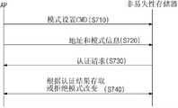
图10是示意性示出根据本发明构思的另一实施例的设置计算系统1000的模式的方法的流程图。参照图1和10,在操作S710中,应用处理器1100将模式设置命令CMD发送给非易失性存储器1200。在操作S720中,应用处理器1100将地址和模式信息发送给非易失性存储器1200。FIG. 10 is a flowchart schematically illustrating a method of setting a mode of a
在操作S730中,非易失性存储器1200将认证请求发送给应用处理器1100。例如,认证请求可要求输入密码和/或认证密钥。在操作S740中,应用处理器1100和非易失性存储器1200根据对认证请求的认证结果来允许或拒绝模式改变。例如,如果认证失败,则非易失性存储器1200拒绝模式改变,并且,如果认证通过,那么非易失性存储器1200允许模式改变。In operation S730, the
通过需要对模式改变的认证,进一步提高非易失性存储器1200的安全。例如,可以进行黑客入侵尝试,以试图将存储体的安全模式或只读模式改变为随机访问模式。但是,通过一旦请求模式改变都产生认证请求并因此需要认证,非易失性存储器1200确保仅仅通过授权的用户执行对存储体的模式改变,从而提高非易失性存储器1200的安全。The security of the
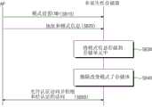
图11是示意性地图示根据本发明构思的另一实施例的设置计算系统1000的模式的方法的流程图。参照图1和11,在操作S810中,应用处理器1100将模式设置命令CMD发送给非易失性存储器1200。在操作S820中,应用处理器1100将地址和模式信息发送给非易失性存储器1200。FIG. 11 is a flowchart schematically illustrating a method of setting a mode of the
在操作S830中,非易失性存储器1200在存储单元中存储模式信息。通过在存储单元中存储模式信息,可以改变选定的存储体的模式。在操作S840中,非易失性存储器1200擦除改变了模式的存储体中的数据。在操作S850中,应用处理器1100和非易失性存储器1200通过允许被认证的(授权的)存取并拒绝未经认证的(未经授权的)存取和拒绝未经授权的存取,来相互通信。In operation S830, the
在参照图11描述的实施例中,在改变了模式的存储体中存储的数据被擦除。因此,在非易失性存储器1200的模式通过黑客入侵或某一其它未经授权的手段而改变的情况中,可以防止在具有例如安全模式或只读模式的存储体中存储的数据被泄露。In the embodiment described with reference to FIG. 11, data stored in a bank whose mode has been changed is erased. Therefore, in the case where the mode of the
通过组合参照图10和11描述的实施例,可以进一步提高非易失性存储器1200的安全。也就是说,需要认证来改变模式,并且,改变了模式的存储体的数据被擦除。By combining the embodiments described with reference to FIGS. 10 and 11 , the security of the
图12是示意性示出根据本发明构思的另一实施例的设置计算系统1000的模式的方法的流程图。参照图1、3和12,在操作S710中,应用处理器1100将地址发送给非易失性存储器1200。在操作S910中,应用处理器1100可以发送将被存取的非易失性存储器1200的存储器单元的地址。FIG. 12 is a flowchart schematically illustrating a method of setting a mode of the
在操作S920中,应用处理器1100将存取命令CMD和模式信息发送给非易失性存储器1200。模式信息可以包括分别对应于参照图3描述的读使能信号RE和写使能信号WE的读使能信息和写使能信息。也就是说,应用处理器1100可以直接向非易失性存储器1200提供与对应于地址的存储体的写许可、写禁止、读许可或读禁止相关联的信息。非易失性存储器1200在存储单元S1至Sn中存储模式信息,并且根据模式信息在内部产生读使能信号RE和写使能信号WE。In operation S920 , the
在操作S930中,非易失性存储器1200基于模式信息来处理输入的存取命令CMD。例如,非易失性存储器1200可以针对对应于输入地址的存储体或RW电路产生分别与输入的读使能信息和写使能信息相对应的读使能信号RE和写使能信号WE。In operation S930, the
在示意性实施例中,应用处理器1100在非易失性存储器1200的存储器映射图(memory map)中存储例如参照图5描述的模式信息。应用处理器1100管理关于非易失性存储器1200的区域是否具有随机存取模式、只读模式、安全模式或易失性模式的信息。应用处理器1100基于管理的模式信息来控制非易失性存储器1200。In an exemplary embodiment, the
在示意性实施例中,当从上层(例如,OS等)接收到的命令与在存储器映射图中存储的模式信息相矛盾时,应用处理器1100可以拒绝输入的命令。In an exemplary embodiment, when a command received from an upper layer (eg, OS, etc.) contradicts mode information stored in the memory map, the
在操作S940中,非易失性存储器1200向应用处理器1100发送对处理的命令的响应。In operation S940 , the
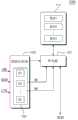
图13是示意性示出根据本发明构思的实施例的存储器系统2000的框图。参照图13,存储器系统2000包括控制器2100和非易失性存储器2200。FIG. 13 is a block diagram schematically illustrating a
控制器2100被构造为将地址ADDR、控制信号CTRL和命令CMD发送给非易失性存储器2200并与非易失性存储器2200交换数据DATA。The
非易失性存储器2200包括多个存储体111至11n。非易失性存储器2200可被构造为基本上与图3中图示的非易失性存储器1200相同,并且,非易失性存储器2200可以以与图3中图示的方式基本上相同的方式操作。The
与上面参照图1至12讨论的应用处理器1100一样,控制器2100被构造为控制非易失性存储器2200的存储体111至11n的操作模式。例如,控制器2100可以在外部主机的控制下控制非易失性存储器2200的存储体111至11n的操作模式。Like the
上述的实施例在非易失性存储器1200和2200包括多个存储体111至11n的条件下被描述。但是,本发明构思并不局限于此。例如,如图14所示,非易失性存储器3200可以包括多个存储器块BLK,且每一个存储器块具有多个存储器单元。存储器块可以是共享外围电路来执行读、写或擦除操作的存储器单元的集合。这些存储器块BLK可能不会同时执行读、写或擦除。从这些存储器块选择的一个存储器块可以执行读、写或擦除。在示意性实施例中,存储体可以包括多个存储器块。同样地,可以通过诸如上面讨论的随机存取模式、只读模式、安全模式和易失性模式等的各种操作模式控制非易失性存储器3200的存储器块BLK。逻辑控制器130’包括分别对应于存储器块的存储单元S1至Sn。逻辑控制器130’可以响应于从外部装置接收到的地址ADDR来参考对应于选定的存储器块的存储单元。逻辑控制器130’被构造为根据参考结果来选择性地激活或去激活读使能信号RE和写使能信号WE。例如,逻辑控制器130’可以基于在对应于地址ADDR的存储单元中存储的模式信息来控制如图5中描述的信号。The above-described embodiments are described on the condition that the
在示意性实施例中,非易失性存储器可以按照存储体或者存储器块单位来控制模式。非易失性存储器可以按照存储体单位来控制存储体的一部分的模式。非易失性存储器可以按照存储器块单位来控制剩余的存储体的模式。此时,存储单元可以一起存储指示存储体或存储器块的地址作为附加模式信息。逻辑控制器基于与从外部装置接收到的地址对应的存储单元来按照存储体或存储器块单位控制模式。In an exemplary embodiment, a nonvolatile memory may control a mode in a bank or memory block unit. The nonvolatile memory can control the mode of a part of the bank on a bank-by-bank basis. The nonvolatile memory can control the mode of the remaining banks in units of memory blocks. At this time, the storage unit may store together an address indicating a bank or a memory block as additional mode information. The logic controller controls a mode in a bank or memory block unit based on a memory unit corresponding to an address received from an external device.
虽然针对示例性实施例描述了本发明构思,但是对于本领域的技术人员来说将会显而易见的是,可以在不脱离本发明的精神和范围的情况下进行各种改变和修改。因此,应该理解,上述实施例不是限制性的,而是说明性的。While the inventive concept has been described with respect to exemplary embodiments, it will be apparent to those skilled in the art that various changes and modifications can be made without departing from the spirit and scope of the invention. Therefore, it should be understood that the above-described embodiments are not restrictive, but illustrative.
Claims (25)
Translated fromChineseApplications Claiming Priority (2)
| Application Number | Priority Date | Filing Date | Title |
|---|---|---|---|
| KR10-2012-0137079 | 2012-11-29 | ||
| KR20120137079AKR20140072276A (en) | 2012-11-29 | 2012-11-29 | Nonvolatile memory and method of operating nonvolatile memory |
Publications (2)
| Publication Number | Publication Date |
|---|---|
| CN103854699Atrue CN103854699A (en) | 2014-06-11 |
| CN103854699B CN103854699B (en) | 2019-02-22 |
Family
ID=50726151
Family Applications (1)
| Application Number | Title | Priority Date | Filing Date |
|---|---|---|---|
| CN201310606617.3AActiveCN103854699B (en) | 2012-11-29 | 2013-11-25 | Non-volatile memory, method of operating the same, and computing device |
Country Status (5)
| Country | Link |
|---|---|
| US (1) | US9076507B2 (en) |
| JP (1) | JP2014107004A (en) |
| KR (1) | KR20140072276A (en) |
| CN (1) | CN103854699B (en) |
| DE (1) | DE102013112897B4 (en) |
Cited By (6)
| Publication number | Priority date | Publication date | Assignee | Title |
|---|---|---|---|---|
| CN108780427A (en)* | 2016-03-04 | 2018-11-09 | 英特尔公司 | Techniques for causing a content pattern to be stored to a memory unit of a memory device |
| CN108932960A (en)* | 2017-05-29 | 2018-12-04 | 三星电子株式会社 | Method of controlling on-chip terminator and system for implementing the method |
| CN110600069A (en)* | 2018-06-12 | 2019-12-20 | 爱思开海力士有限公司 | Memory system having memory device and memory controller and method of operating the same |
| CN112233716A (en)* | 2020-09-27 | 2021-01-15 | 加特兰微电子科技(上海)有限公司 | Memories, storage devices, integrated circuits, radio devices and equipment |
| CN112882660A (en)* | 2021-03-08 | 2021-06-01 | 吴曼青 | Secure storage device |
| CN115050400A (en)* | 2022-06-27 | 2022-09-13 | 清华大学 | Writing method and writing device of memory |
Families Citing this family (3)
| Publication number | Priority date | Publication date | Assignee | Title |
|---|---|---|---|---|
| JP7196511B2 (en)* | 2018-10-01 | 2022-12-27 | 富士フイルムビジネスイノベーション株式会社 | data processor |
| US12068015B2 (en) | 2021-11-15 | 2024-08-20 | Samsung Electronics Co., Ltd. | Memory device including merged write driver |
| CN117931702B (en)* | 2024-03-20 | 2024-06-07 | 中国科学院国家空间科学中心 | Off-chip system of system-level chip and application program solidifying method |
Citations (2)
| Publication number | Priority date | Publication date | Assignee | Title |
|---|---|---|---|---|
| CN1613063A (en)* | 2002-01-09 | 2005-05-04 | 株式会社瑞萨科技 | Storage Systems and Memory Cards |
| US20120131258A1 (en)* | 2010-11-18 | 2012-05-24 | Hynix Semiconductor Inc. | Semiconductor memory apparatus and method for operating the same |
Family Cites Families (25)
| Publication number | Priority date | Publication date | Assignee | Title |
|---|---|---|---|---|
| US4099253A (en)* | 1976-09-13 | 1978-07-04 | Dynage, Incorporated | Random access memory with bit or byte addressing capability |
| JPS6057090B2 (en)* | 1980-09-19 | 1985-12-13 | 株式会社日立製作所 | Data storage device and processing device using it |
| US5594704A (en)* | 1992-04-27 | 1997-01-14 | Mitsubishi Denki Kabushiki Kaisha | Synchronous semiconductor memory device |
| JPH1165936A (en)* | 1997-06-12 | 1999-03-09 | Oki Micro Design Miyazaki:Kk | Memory device |
| US6011727A (en)* | 1998-08-26 | 2000-01-04 | Micron Technology, Inc. | Block write circuit and method for wide data path memory devices |
| JP3734408B2 (en)* | 2000-07-03 | 2006-01-11 | シャープ株式会社 | Semiconductor memory device |
| US6985388B2 (en)* | 2001-09-17 | 2006-01-10 | Sandisk Corporation | Dynamic column block selection |
| JP2003271457A (en) | 2002-03-14 | 2003-09-26 | Sanyo Electric Co Ltd | Data storage device |
| US7073026B2 (en)* | 2002-11-26 | 2006-07-04 | Advanced Micro Devices, Inc. | Microprocessor including cache memory supporting multiple accesses per cycle |
| CN101036197A (en)* | 2004-11-10 | 2007-09-12 | 松下电器产业株式会社 | Non-volatile memory device for matching memory controllers with different numbers of memory banks to be accessed simultaneously |
| KR100722658B1 (en) | 2005-02-14 | 2007-05-28 | 최명렬 | Memory device and its control method |
| US20060218425A1 (en)* | 2005-02-25 | 2006-09-28 | Zhimin Ding | Integrated microcontroller and memory with secure interface between system program and user operating system and application |
| JP4989872B2 (en) | 2005-10-13 | 2012-08-01 | ルネサスエレクトロニクス株式会社 | Semiconductor memory device and arithmetic processing unit |
| KR20070074232A (en) | 2006-01-09 | 2007-07-12 | 삼성전자주식회사 | Semiconductor memory device having both RAM and ROM regions |
| US7728622B2 (en) | 2007-03-29 | 2010-06-01 | Qualcomm Incorporated | Software programmable logic using spin transfer torque magnetoresistive random access memory |
| JP2009009279A (en) | 2007-06-27 | 2009-01-15 | Panasonic Corp | Memory controller, nonvolatile memory module, and nonvolatile memory system |
| JP2009151386A (en) | 2007-12-18 | 2009-07-09 | Ricoh Co Ltd | Image processing device |
| KR20090067649A (en) | 2007-12-21 | 2009-06-25 | 삼성전자주식회사 | Memory system having a secure storage device and its security area management method |
| KR20100013824A (en) | 2008-08-01 | 2010-02-10 | 주식회사 하이닉스반도체 | Solid state storage system with high speed |
| US7974124B2 (en)* | 2009-06-24 | 2011-07-05 | Sandisk Corporation | Pointer based column selection techniques in non-volatile memories |
| JP2011008861A (en) | 2009-06-25 | 2011-01-13 | Sony Corp | Memory |
| KR101780422B1 (en) | 2010-11-15 | 2017-09-22 | 삼성전자주식회사 | Nonvolatile memory device, reading method thereof and memory system including the same |
| KR101284565B1 (en) | 2011-06-10 | 2013-07-11 | 주식회사 린노 | illumination apparatus of side light emitting type |
| KR20130098681A (en)* | 2012-02-28 | 2013-09-05 | 삼성전자주식회사 | Semiconductor memory device |
| US9641464B2 (en)* | 2012-04-30 | 2017-05-02 | Nxp Usa, Inc. | FIFO buffer system providing same clock cycle response to pop commands |
- 2012
- 2012-11-29KRKR20120137079Apatent/KR20140072276A/ennot_activeWithdrawn
- 2013
- 2013-11-18USUS14/082,210patent/US9076507B2/enactiveActive
- 2013-11-22JPJP2013241704Apatent/JP2014107004A/enactivePending
- 2013-11-22DEDE102013112897.1Apatent/DE102013112897B4/enactiveActive
- 2013-11-25CNCN201310606617.3Apatent/CN103854699B/enactiveActive
Patent Citations (2)
| Publication number | Priority date | Publication date | Assignee | Title |
|---|---|---|---|---|
| CN1613063A (en)* | 2002-01-09 | 2005-05-04 | 株式会社瑞萨科技 | Storage Systems and Memory Cards |
| US20120131258A1 (en)* | 2010-11-18 | 2012-05-24 | Hynix Semiconductor Inc. | Semiconductor memory apparatus and method for operating the same |
Cited By (10)
| Publication number | Priority date | Publication date | Assignee | Title |
|---|---|---|---|---|
| CN108780427A (en)* | 2016-03-04 | 2018-11-09 | 英特尔公司 | Techniques for causing a content pattern to be stored to a memory unit of a memory device |
| CN108780427B (en)* | 2016-03-04 | 2023-07-14 | 英特尔公司 | Techniques for causing a content pattern to be stored to a memory unit of a memory device |
| CN108932960A (en)* | 2017-05-29 | 2018-12-04 | 三星电子株式会社 | Method of controlling on-chip terminator and system for implementing the method |
| CN108932960B (en)* | 2017-05-29 | 2021-06-01 | 三星电子株式会社 | Method for controlling on-chip terminator and system for executing the same |
| US11475930B2 (en) | 2017-05-29 | 2022-10-18 | Samsung Electronics Co., Ltd. | Method of controlling on-die termination and system performing the same |
| CN110600069A (en)* | 2018-06-12 | 2019-12-20 | 爱思开海力士有限公司 | Memory system having memory device and memory controller and method of operating the same |
| CN110600069B (en)* | 2018-06-12 | 2023-10-10 | 爱思开海力士有限公司 | Memory system having memory device and memory controller and method of operating the same |
| CN112233716A (en)* | 2020-09-27 | 2021-01-15 | 加特兰微电子科技(上海)有限公司 | Memories, storage devices, integrated circuits, radio devices and equipment |
| CN112882660A (en)* | 2021-03-08 | 2021-06-01 | 吴曼青 | Secure storage device |
| CN115050400A (en)* | 2022-06-27 | 2022-09-13 | 清华大学 | Writing method and writing device of memory |
Also Published As
| Publication number | Publication date |
|---|---|
| DE102013112897A1 (en) | 2014-06-05 |
| JP2014107004A (en) | 2014-06-09 |
| KR20140072276A (en) | 2014-06-13 |
| US20140146621A1 (en) | 2014-05-29 |
| DE102013112897B4 (en) | 2022-09-08 |
| CN103854699B (en) | 2019-02-22 |
| US9076507B2 (en) | 2015-07-07 |
Similar Documents
| Publication | Publication Date | Title |
|---|---|---|
| CN103854699A (en) | Nonvolatile memory, operating method thereof and calculation device | |
| US10783252B2 (en) | System and method for booting within a heterogeneous memory environment | |
| US9037824B2 (en) | Password accessible microelectronic memory | |
| US10257192B2 (en) | Storage system and method for performing secure write protect thereof | |
| US9378396B2 (en) | Storage device and memory controller thereof | |
| US12379954B2 (en) | Protected regions management of memory | |
| KR20130134918A (en) | Computer system having non-volatile memory and operating method thereof | |
| JP2017518558A (en) | Apparatus and method for securing an access protection scheme | |
| US10372629B2 (en) | Control for authenticated accesses to a memory device | |
| JP2020030527A (en) | Storage device and program | |
| EP3961451B1 (en) | Storage device | |
| TW202213107A (en) | Storage device, host device, electronic device including storage device and host device, and method of operating the same | |
| US20220230688A1 (en) | Memory devices and methods of processing security data thereof | |
| CN108228486B (en) | Method of operating a memory system | |
| KR20220021800A (en) | Storage device and operating method thereof | |
| US20230136229A1 (en) | Storage device, computing system, and method of operating the same | |
| US20130151832A1 (en) | Flash memory storage system and data protection method thereof | |
| JP5894044B2 (en) | Method and portable computer for storing data in a hybrid disk drive | |
| US12436690B2 (en) | Memory controller and storage device | |
| US20120137089A1 (en) | Storage device, electronic device, and access control method for storage device | |
| KR101938875B1 (en) | Mobile memory mounting test device | |
| HK40025631A (en) | System and method for booting within a heterogeneous memory environment |
Legal Events
| Date | Code | Title | Description |
|---|---|---|---|
| C06 | Publication | ||
| PB01 | Publication | ||
| C10 | Entry into substantive examination | ||
| SE01 | Entry into force of request for substantive examination | ||
| GR01 | Patent grant | ||
| GR01 | Patent grant |