CN103843118A - Insensitive dry removal process for semiconductor integration - Google Patents
Insensitive dry removal process for semiconductor integrationDownload PDFInfo
- Publication number
- CN103843118A CN103843118ACN201280048556.7ACN201280048556ACN103843118ACN 103843118 ACN103843118 ACN 103843118ACN 201280048556 ACN201280048556 ACN 201280048556ACN 103843118 ACN103843118 ACN 103843118A
- Authority
- CN
- China
- Prior art keywords
- dielectric layer
- etch rate
- dielectric
- deposited
- wet etch
- Prior art date
- Legal status (The legal status is an assumption and is not a legal conclusion. Google has not performed a legal analysis and makes no representation as to the accuracy of the status listed.)
- Pending
Links
- 238000000034methodMethods0.000titleclaimsabstractdescription126
- 239000004065semiconductorSubstances0.000titleclaimsabstractdescription20
- 230000008569processEffects0.000titleclaimsdescription54
- 230000010354integrationEffects0.000titledescription3
- 239000000758substrateSubstances0.000claimsabstractdescription65
- 238000000151depositionMethods0.000claimsabstractdescription57
- 238000005530etchingMethods0.000claimsabstractdescription37
- 230000009969flowable effectEffects0.000claimsabstractdescription37
- 239000000203mixtureSubstances0.000claimsabstractdescription32
- 239000007789gasSubstances0.000claimsdescription59
- 239000003989dielectric materialSubstances0.000claimsdescription52
- QGZKDVFQNNGYKY-UHFFFAOYSA-NAmmoniaChemical compoundNQGZKDVFQNNGYKY-UHFFFAOYSA-N0.000claimsdescription16
- 229910021529ammoniaInorganic materials0.000claimsdescription7
- QKCGXXHCELUCKW-UHFFFAOYSA-Nn-[4-[4-(dinaphthalen-2-ylamino)phenyl]phenyl]-n-naphthalen-2-ylnaphthalen-2-amineChemical compoundC1=CC=CC2=CC(N(C=3C=CC(=CC=3)C=3C=CC(=CC=3)N(C=3C=C4C=CC=CC4=CC=3)C=3C=C4C=CC=CC4=CC=3)C3=CC4=CC=CC=C4C=C3)=CC=C21QKCGXXHCELUCKW-UHFFFAOYSA-N0.000claimsdescription6
- YCKRFDGAMUMZLT-UHFFFAOYSA-NFluorine atomChemical compound[F]YCKRFDGAMUMZLT-UHFFFAOYSA-N0.000claimsdescription5
- 229910052731fluorineInorganic materials0.000claimsdescription5
- 239000011737fluorineSubstances0.000claimsdescription5
- 239000011521glassSubstances0.000claimsdescription5
- 239000002184metalSubstances0.000claimsdescription4
- 238000005137deposition processMethods0.000claims4
- 238000002207thermal evaporationMethods0.000claims2
- 230000008021depositionEffects0.000abstractdescription32
- 239000010410layerSubstances0.000description145
- 239000000463materialSubstances0.000description40
- 239000002243precursorSubstances0.000description37
- IJGRMHOSHXDMSA-UHFFFAOYSA-NAtomic nitrogenChemical compoundN#NIJGRMHOSHXDMSA-UHFFFAOYSA-N0.000description20
- 229910021420polycrystalline siliconInorganic materials0.000description15
- 229920005591polysiliconPolymers0.000description15
- 238000012545processingMethods0.000description15
- XUIMIQQOPSSXEZ-UHFFFAOYSA-NSiliconChemical compound[Si]XUIMIQQOPSSXEZ-UHFFFAOYSA-N0.000description13
- 229910052710siliconInorganic materials0.000description13
- 239000010703siliconSubstances0.000description13
- 239000011229interlayerSubstances0.000description12
- 229910052757nitrogenInorganic materials0.000description12
- QJGQUHMNIGDVPM-UHFFFAOYSA-Nnitrogen groupChemical group[N]QJGQUHMNIGDVPM-UHFFFAOYSA-N0.000description12
- 238000004519manufacturing processMethods0.000description11
- 125000006850spacer groupChemical group0.000description11
- 230000015572biosynthetic processEffects0.000description8
- 229910017840NH 3Inorganic materials0.000description7
- 150000004767nitridesChemical class0.000description7
- 239000012686silicon precursorSubstances0.000description7
- OKTJSMMVPCPJKN-UHFFFAOYSA-NCarbonChemical compound[C]OKTJSMMVPCPJKN-UHFFFAOYSA-N0.000description6
- 229910052799carbonInorganic materials0.000description6
- 229910052760oxygenInorganic materials0.000description6
- OAKJQQAXSVQMHS-UHFFFAOYSA-NHydrazineChemical compoundNNOAKJQQAXSVQMHS-UHFFFAOYSA-N0.000description5
- QVGXLLKOCUKJST-UHFFFAOYSA-Natomic oxygenChemical compound[O]QVGXLLKOCUKJST-UHFFFAOYSA-N0.000description5
- 238000006243chemical reactionMethods0.000description5
- 238000010586diagramMethods0.000description5
- 239000001301oxygenSubstances0.000description5
- 150000003254radicalsChemical class0.000description5
- 239000000376reactantSubstances0.000description5
- 239000000243solutionSubstances0.000description5
- 239000002019doping agentSubstances0.000description4
- 238000005516engineering processMethods0.000description4
- 229910052734heliumInorganic materials0.000description4
- 239000001257hydrogenSubstances0.000description4
- 229910052739hydrogenInorganic materials0.000description4
- 229920003209poly(hydridosilsesquioxane)Polymers0.000description4
- 238000001039wet etchingMethods0.000description4
- BOTDANWDWHJENH-UHFFFAOYSA-NTetraethyl orthosilicateChemical compoundCCO[Si](OCC)(OCC)OCCBOTDANWDWHJENH-UHFFFAOYSA-N0.000description3
- 238000000137annealingMethods0.000description3
- 230000015556catabolic processEffects0.000description3
- 238000009792diffusion processMethods0.000description3
- 239000001307heliumSubstances0.000description3
- SWQJXJOGLNCZEY-UHFFFAOYSA-Nhelium atomChemical compound[He]SWQJXJOGLNCZEY-UHFFFAOYSA-N0.000description3
- 238000002955isolationMethods0.000description3
- 150000002831nitrogen free-radicalsChemical class0.000description3
- 239000000126substanceSubstances0.000description3
- XKRFYHLGVUSROY-UHFFFAOYSA-NArgonChemical compound[Ar]XKRFYHLGVUSROY-UHFFFAOYSA-N0.000description2
- -1H 2 N(SiH 3 )Chemical class0.000description2
- UFHFLCQGNIYNRP-UHFFFAOYSA-NHydrogenChemical compound[H][H]UFHFLCQGNIYNRP-UHFFFAOYSA-N0.000description2
- BLRPTPMANUNPDV-UHFFFAOYSA-NSilaneChemical compound[SiH4]BLRPTPMANUNPDV-UHFFFAOYSA-N0.000description2
- VYPSYNLAJGMNEJ-UHFFFAOYSA-NSilicium dioxideChemical compoundO=[Si]=OVYPSYNLAJGMNEJ-UHFFFAOYSA-N0.000description2
- 238000003917TEM imageMethods0.000description2
- 229910052786argonInorganic materials0.000description2
- 230000008901benefitEffects0.000description2
- 239000012159carrier gasSubstances0.000description2
- 150000001875compoundsChemical class0.000description2
- 238000001816coolingMethods0.000description2
- 230000007547defectEffects0.000description2
- 238000010438heat treatmentMethods0.000description2
- 239000007943implantSubstances0.000description2
- 230000007246mechanismEffects0.000description2
- 229920000642polymerPolymers0.000description2
- 238000001878scanning electron micrographMethods0.000description2
- FZHAPNGMFPVSLP-UHFFFAOYSA-NsilanamineChemical class[SiH3]NFZHAPNGMFPVSLP-UHFFFAOYSA-N0.000description2
- 229910000077silaneInorganic materials0.000description2
- 229910052814silicon oxideInorganic materials0.000description2
- ZOXJGFHDIHLPTG-UHFFFAOYSA-NBoronChemical compound[B]ZOXJGFHDIHLPTG-UHFFFAOYSA-N0.000description1
- KRHYYFGTRYWZRS-UHFFFAOYSA-NFluoraneChemical compoundFKRHYYFGTRYWZRS-UHFFFAOYSA-N0.000description1
- CBENFWSGALASAD-UHFFFAOYSA-NOzoneChemical compound[O-][O+]=OCBENFWSGALASAD-UHFFFAOYSA-N0.000description1
- OAICVXFJPJFONN-UHFFFAOYSA-NPhosphorusChemical compound[P]OAICVXFJPJFONN-UHFFFAOYSA-N0.000description1
- 229910052581Si3N4Inorganic materials0.000description1
- 239000007864aqueous solutionSubstances0.000description1
- 229910052796boronInorganic materials0.000description1
- 239000006227byproductSubstances0.000description1
- 239000003795chemical substances by applicationSubstances0.000description1
- 230000000052comparative effectEffects0.000description1
- 238000010276constructionMethods0.000description1
- 238000011109contaminationMethods0.000description1
- 238000011161developmentMethods0.000description1
- PZPGRFITIJYNEJ-UHFFFAOYSA-NdisilaneChemical compound[SiH3][SiH3]PZPGRFITIJYNEJ-UHFFFAOYSA-N0.000description1
- 229910000040hydrogen fluorideInorganic materials0.000description1
- 238000002513implantationMethods0.000description1
- 239000012535impuritySubstances0.000description1
- 238000009413insulationMethods0.000description1
- 238000001465metallisationMethods0.000description1
- 238000013508migrationMethods0.000description1
- 230000005012migrationEffects0.000description1
- 238000012986modificationMethods0.000description1
- 230000004048modificationEffects0.000description1
- 229910000069nitrogen hydrideInorganic materials0.000description1
- 229910052756noble gasInorganic materials0.000description1
- 150000002835noble gasesChemical class0.000description1
- 238000007254oxidation reactionMethods0.000description1
- 230000001590oxidative effectEffects0.000description1
- 238000005192partitionMethods0.000description1
- 229910052698phosphorusInorganic materials0.000description1
- 239000011574phosphorusSubstances0.000description1
- 229920002120photoresistant polymerPolymers0.000description1
- 238000000623plasma-assisted chemical vapour depositionMethods0.000description1
- 238000007517polishing processMethods0.000description1
- 238000002360preparation methodMethods0.000description1
- 239000000047productSubstances0.000description1
- 239000011241protective layerSubstances0.000description1
- 150000003377silicon compoundsChemical class0.000description1
- HQVNEWCFYHHQES-UHFFFAOYSA-Nsilicon nitrideChemical compoundN12[Si]34N5[Si]62N3[Si]51N64HQVNEWCFYHHQES-UHFFFAOYSA-N0.000description1
- 239000007787solidSubstances0.000description1
- 238000000859sublimationMethods0.000description1
- 230000008022sublimationEffects0.000description1
- 238000012546transferMethods0.000description1
Images

Classifications
- H—ELECTRICITY
- H01—ELECTRIC ELEMENTS
- H01L—SEMICONDUCTOR DEVICES NOT COVERED BY CLASS H10
- H01L21/00—Processes or apparatus adapted for the manufacture or treatment of semiconductor or solid state devices or of parts thereof
- H01L21/02—Manufacture or treatment of semiconductor devices or of parts thereof
- H01L21/02104—Forming layers
- H01L21/02365—Forming inorganic semiconducting materials on a substrate
- H01L21/02612—Formation types
- H01L21/02617—Deposition types
- H01L21/0262—Reduction or decomposition of gaseous compounds, e.g. CVD
- H—ELECTRICITY
- H01—ELECTRIC ELEMENTS
- H01L—SEMICONDUCTOR DEVICES NOT COVERED BY CLASS H10
- H01L21/00—Processes or apparatus adapted for the manufacture or treatment of semiconductor or solid state devices or of parts thereof
- H01L21/02—Manufacture or treatment of semiconductor devices or of parts thereof
- H01L21/04—Manufacture or treatment of semiconductor devices or of parts thereof the devices having potential barriers, e.g. a PN junction, depletion layer or carrier concentration layer
- H01L21/18—Manufacture or treatment of semiconductor devices or of parts thereof the devices having potential barriers, e.g. a PN junction, depletion layer or carrier concentration layer the devices having semiconductor bodies comprising elements of Group IV of the Periodic Table or AIIIBV compounds with or without impurities, e.g. doping materials
- H01L21/30—Treatment of semiconductor bodies using processes or apparatus not provided for in groups H01L21/20 - H01L21/26
- H01L21/302—Treatment of semiconductor bodies using processes or apparatus not provided for in groups H01L21/20 - H01L21/26 to change their surface-physical characteristics or shape, e.g. etching, polishing, cutting
- H01L21/306—Chemical or electrical treatment, e.g. electrolytic etching
- H01L21/3065—Plasma etching; Reactive-ion etching
- H—ELECTRICITY
- H01—ELECTRIC ELEMENTS
- H01L—SEMICONDUCTOR DEVICES NOT COVERED BY CLASS H10
- H01L21/00—Processes or apparatus adapted for the manufacture or treatment of semiconductor or solid state devices or of parts thereof
- H01L21/02—Manufacture or treatment of semiconductor devices or of parts thereof
- H01L21/04—Manufacture or treatment of semiconductor devices or of parts thereof the devices having potential barriers, e.g. a PN junction, depletion layer or carrier concentration layer
- H01L21/18—Manufacture or treatment of semiconductor devices or of parts thereof the devices having potential barriers, e.g. a PN junction, depletion layer or carrier concentration layer the devices having semiconductor bodies comprising elements of Group IV of the Periodic Table or AIIIBV compounds with or without impurities, e.g. doping materials
- H01L21/30—Treatment of semiconductor bodies using processes or apparatus not provided for in groups H01L21/20 - H01L21/26
- H01L21/31—Treatment of semiconductor bodies using processes or apparatus not provided for in groups H01L21/20 - H01L21/26 to form insulating layers thereon, e.g. for masking or by using photolithographic techniques; After treatment of these layers; Selection of materials for these layers
- H01L21/3105—After-treatment
- H01L21/311—Etching the insulating layers by chemical or physical means
- H01L21/31105—Etching inorganic layers
- H01L21/31111—Etching inorganic layers by chemical means
- H01L21/31116—Etching inorganic layers by chemical means by dry-etching
- H—ELECTRICITY
- H10—SEMICONDUCTOR DEVICES; ELECTRIC SOLID-STATE DEVICES NOT OTHERWISE PROVIDED FOR
- H10D—INORGANIC ELECTRIC SEMICONDUCTOR DEVICES
- H10D64/00—Electrodes of devices having potential barriers
- H10D64/01—Manufacture or treatment
- H10D64/017—Manufacture or treatment using dummy gates in processes wherein at least parts of the final gates are self-aligned to the dummy gates, i.e. replacement gate processes
- H—ELECTRICITY
- H10—SEMICONDUCTOR DEVICES; ELECTRIC SOLID-STATE DEVICES NOT OTHERWISE PROVIDED FOR
- H10D—INORGANIC ELECTRIC SEMICONDUCTOR DEVICES
- H10D64/00—Electrodes of devices having potential barriers
- H10D64/01—Manufacture or treatment
- H10D64/031—Manufacture or treatment of data-storage electrodes
- H10D64/035—Manufacture or treatment of data-storage electrodes comprising conductor-insulator-conductor-insulator-semiconductor structures
Landscapes
- Engineering & Computer Science (AREA)
- Chemical & Material Sciences (AREA)
- Physics & Mathematics (AREA)
- Manufacturing & Machinery (AREA)
- Condensed Matter Physics & Semiconductors (AREA)
- General Physics & Mathematics (AREA)
- Computer Hardware Design (AREA)
- Microelectronics & Electronic Packaging (AREA)
- Power Engineering (AREA)
- Inorganic Chemistry (AREA)
- General Chemical & Material Sciences (AREA)
- Chemical Kinetics & Catalysis (AREA)
- Plasma & Fusion (AREA)
- Drying Of Semiconductors (AREA)
- Weting (AREA)
- Insulated Gate Type Field-Effect Transistor (AREA)
Abstract
Translated fromChineseDescription
Translated fromChinese相关申请案的交叉引用Cross References to Related Applications
此申请是2012年9月21日提交的、题为“INSENSITIVE DRY REMOVALPROCESS FOR SEMICONDUCTOR INTEGRATION(用于半导体整合的不敏感干法移除工艺)”的美国专利申请No.13/624,693的PCT申请,并且涉及并要求2011年9月26日提交的、题为“INSENSITIVE DRY REMOVAL PROCESSFOR SEMICONDUCTOR INTEGRATION(用于半导体整合的不敏感干法移除工艺)”的美国临时专利申请No.61/539,270号的权益,上述两个申请出于所有目的通过整体引用结合于此。This application is a PCT application of U.S. Patent Application No. 13/624,693, filed September 21, 2012, entitled "INSENSITIVE DRY REMOVAL PROCESS FOR SEMICONDUCTOR INTEGRATION" and Relating to and claiming the benefit of U.S. Provisional Patent Application No. 61/539,270, entitled "INSENSITIVE DRY REMOVAL PROCESSFOR SEMICONDUCTOR INTEGRATION," filed September 26, 2011, Both of the aforementioned applications are hereby incorporated by reference in their entirety for all purposes.
背景background
半导体处理通常包括多个不同的制造步骤。在当前技术下,可例行地在纳米尺寸上形成电路部件且需要敏感性制造技术。举例而言,在替换式金属栅极(“RMG”或“后栅极(gate last)”)处理中,可能需要在基板上的非牺牲材料的存在的情况下移除位于沟槽中或位于半导体基板上的另一特征结构中的牺牲材料。用于移除第一材料的蚀刻技术可能将第一材料与第二材料两者暴露于蚀刻剂,蚀刻剂可能会移除牺牲材料与非牺牲材料两者。若在移除牺牲材料之前移除太多或所有的非牺牲材料,则可能会弄坏基板。Semiconductor processing often includes a number of different manufacturing steps. With current technology, circuit components are routinely formed on nanometer scales and require sensitive fabrication techniques. For example, in replacement metal gate ("RMG" or "gate last") processing, it may be necessary to remove the Sacrificial material in another feature on the semiconductor substrate. The etching technique used to remove the first material may expose both the first material and the second material to an etchant, which may remove both sacrificial and non-sacrificial materials. If too much or all of the non-sacrificial material is removed before the sacrificial material is removed, the substrate may be damaged.
由于后栅极处理可包括在已经沉积非牺牲膜之后的牺牲材料移除,因此需要精细与受控制的蚀刻技术。虽然有多种蚀刻技术可用,但很少有蚀刻技术提供的移除可对位于半导体基板上的膜的类型与质量两者负责。举例而言,利用氟化氢溶液的湿法移除可用于多种类型的膜或氧化物移除。然而,这些溶液对已经沉积的材料的密度或质量敏感,且这些溶液可能会移除太多的非牺牲材料。在某些实施例中,湿法蚀刻将会以比较高质量的膜快高达40倍的速率移除较低质量的膜。若较低质量的膜是非牺牲的,则湿法蚀刻移除可能无法在移除太多(若非全部)的非牺牲层之前移除牺牲层。Since gate last processing may include sacrificial material removal after non-sacrificial films have been deposited, delicate and controlled etch techniques are required. While a variety of etching techniques are available, few etch techniques provide removal that is responsible for both the type and quality of the films located on the semiconductor substrate. For example, wet removal using a hydrogen fluoride solution can be used for various types of film or oxide removal. However, these solutions are sensitive to the density or mass of material already deposited, and these solutions may remove too much non-sacrificial material. In certain embodiments, wet etching will remove lower quality films at a rate up to 40 times faster than higher quality films. If the lower quality film is non-sacrificial, wet etch removal may not be able to remove the sacrificial layer before removing too much, if not all, of the non-sacrificial layer.
因此,持续需要在非牺牲膜存在的情况下移除牺牲膜的技术与产物。本发明技术解决这些需求与其它需求。Accordingly, there is a continuing need for techniques and products that remove sacrificial films in the presence of non-sacrificial films. The present technology addresses these needs and others.
简要概述brief overview
本发明技术提供从半导体基板的表面移除介电材料的方法,所述方法实质上对被移除的材料的质量不敏感。藉由应用在实质上相似速率下蚀刻氧化物的干法蚀刻剂气体的组合,可在较低膜质量的非牺牲膜存在的情况下移除较高膜质量的牺牲膜。The present technology provides methods of removing dielectric material from the surface of a semiconductor substrate that are substantially insensitive to the quality of the material being removed. By applying a combination of dry etchant gases that etch oxide at substantially similar rates, a higher film quality sacrificial film can be removed in the presence of a lower film quality non-sacrificial film.
揭露沉积介电层以及从半导体基板的表面蚀刻介电层的方法。方法可包括沉积第一介电层,第一介电层具有HF水溶液中的第一湿法蚀刻速率。方法亦可包括沉积第二介电层,第二介电层在沉积之后最初可为可流动的,且第二介电层可具有HF水溶液中的第二湿法蚀刻速率,第二湿法蚀刻速率高于第一湿法蚀刻速率。方法可进一步包括用蚀刻剂气体混合物蚀刻第一介电层与第二介电层,其中第一介电层与第二介电层的蚀刻速率比率比HF水溶液中的第二湿法蚀刻速率与第一湿法蚀刻速率的比率更接近1。Methods of depositing a dielectric layer and etching the dielectric layer from a surface of a semiconductor substrate are disclosed. Methods can include depositing a first dielectric layer having a first wet etch rate in aqueous HF. The method may also include depositing a second dielectric layer, the second dielectric layer may be flowable initially after deposition, and the second dielectric layer may have a second wet etch rate in aqueous HF, the second wet etch The rate is higher than the first wet etch rate. The method may further include etching the first dielectric layer and the second dielectric layer with an etchant gas mixture, wherein the ratio of the etch rate of the first dielectric layer to the second dielectric layer is greater than the ratio of the second wet etch rate in aqueous HF to The ratio of the first wet etch rate is closer to 1.
技术的实施例亦包括移除半导体基板的表面上的介电材料的方法。方法可被用于后栅极工艺,且方法可包括在基板上沉积第一介电材料以产生第一质量的介电层,第一质量的介电层具有HF水溶液中的第一湿法蚀刻速率。亦可沉积第二介电材料,且第二介电材料在沉积之后最初可为可流动的。可固化第二介电材料以产生第二质量的第二介电层,第二质量的第二介电层具有HF水溶液中的第二湿法蚀刻速率,第二湿法蚀刻速率大于第一湿法蚀刻速率。方法亦可包括用干法蚀刻剂气体混合物蚀刻第一介电层与第二介电层,其中用干法蚀刻剂气体混合物蚀刻的第一介电层与第二介电层的蚀刻速率比率比HF水溶液中的第二湿法蚀刻速率与第一湿法蚀刻速率的比率更接近1。Embodiments of the technique also include methods of removing dielectric material on a surface of a semiconductor substrate. The method may be used in a gate last process, and the method may include depositing a first dielectric material on the substrate to produce a first quality dielectric layer having a first wet etch in aqueous HF rate. A second dielectric material may also be deposited, and may initially be flowable after deposition. The second dielectric material can be cured to produce a second dielectric layer of a second quality having a second wet etch rate in aqueous HF, the second wet etch rate being greater than the first wet etch rate method etch rate. The method may also include etching the first dielectric layer and the second dielectric layer with a dry etchant gas mixture, wherein the etchant rate ratio of the first dielectric layer and the second dielectric layer etched with the dry etchant gas mixture is greater than The ratio of the second wet etch rate to the first wet etch rate in the HF aqueous solution is closer to 1.
在后续描述中提出额外实施例与特征的部分,且本领域技术人员在查看本说明书后和/或藉由实施所揭露方法可得知额外实施例与特征结构的部分。可藉由本说明书中描述的仪器设备、组合和/或方法理解与达成所揭露工艺与方法的特征与优点。Additional embodiments and portions of features are set forth in the ensuing description, and those skilled in the art may learn of additional embodiments and portions of features after reviewing this specification and/or by practicing the disclosed methods. The features and advantages of the disclosed processes and methods can be understood and achieved by means of the apparatuses, combinations and/or methods described in this specification.
附图简述Brief description of the drawings
图1图示已经执行假栅极(dummy gate)移除工艺于基板上的基板的横剖面图。FIG. 1 illustrates a cross-sectional view of a substrate on which a dummy gate removal process has been performed.
图2图示根据揭露方法的蚀刻工艺的流程图。FIG. 2 illustrates a flow diagram of an etching process according to the disclosed method.
图3图示根据揭露方法的蚀刻工艺的流程图。3 illustrates a flow diagram of an etching process according to the disclosed method.
图4图示已经在基板上执行根据本方法的蚀刻工艺的基板的横剖面图。FIG. 4 illustrates a cross-sectional view of a substrate on which an etching process according to the present method has been performed.
图5A图示湿法凹陷蚀刻工艺的TEM图像。FIG. 5A illustrates a TEM image of a wet recess etch process.
图5B图示已经在基板上执行根据揭露方法的蚀刻工艺的基板的TEM图像。FIG. 5B illustrates a TEM image of a substrate on which an etching process according to the disclosed method has been performed.
详细描述A detailed description
描述在较低质量的非牺牲膜存在的情况下蚀刻较高质量的牺牲膜的方法。藉由利用实质上对被接受蚀刻的介电层的质量不敏感的干法蚀刻剂,可在第二质量的非牺牲膜存在的情况下移除第一质量的牺牲膜。A method of etching a higher quality sacrificial film in the presence of a lower quality non-sacrificial film is described. By utilizing a dry etchant that is substantially insensitive to the quality of the dielectric layer being etched, a first mass of sacrificial film can be removed in the presence of a second mass of non-sacrificial film.
揭露沉积介电层与自半导体基板的表面蚀刻介电层的方法。方法可包括沉积第一介电层,第一介电层具有HF水溶液中的第一湿法蚀刻速率。方法亦可包括沉积第二介电层,第二介电层在沉积之后最初可为可流动的,且第二介电层可具有HF水溶液中的第二湿法蚀刻速率,第二湿法蚀刻速率高于第一湿法蚀刻速率。方法可进一步包括用蚀刻剂气体混合物蚀刻第一介电层与第二介电层,其中第一介电层与第二介电层的蚀刻速率比率比起HF水溶液中的第二湿法蚀刻速率与第一湿法蚀刻速率的比率更接近1。Methods of depositing and etching a dielectric layer from a surface of a semiconductor substrate are disclosed. Methods can include depositing a first dielectric layer having a first wet etch rate in aqueous HF. The method may also include depositing a second dielectric layer, the second dielectric layer may be flowable initially after deposition, and the second dielectric layer may have a second wet etch rate in aqueous HF, the second wet etch The rate is higher than the first wet etch rate. The method may further comprise etching the first dielectric layer and the second dielectric layer with an etchant gas mixture, wherein the ratio of the etch rate of the first dielectric layer to the second dielectric layer is greater than the second wet etch rate in the aqueous HF solution The ratio to the first wet etch rate is closer to 1.
参照图1,图示已经在半导体基板上执行假栅极移除工艺的半导体基板的横剖面图。针对基板100,图示包括沟槽110的硅基板105。沉积第一介电层115以隔离硅基板105。可将电介质沉积成基板上的连续层。沉积假栅极120于第一介电层115上,接着藉由对假栅极与上有假栅极的电介质两者的蚀刻来形成岛或隔离栅极。电介质可为氧化物、氮化物或氮氧化物,且可藉由多种手段来沉积电介质。电介质沉积物可为热氧化物或HDP-CVD沉积的电介质或者介电沉积物替代地可为SACVD沉积的电介质。或者,可藉由提供用于绝缘目的的相对高质量氧化物的不同技术来沉积电介质。假栅极可为后续可移除的任何材料。举例而言,假栅极可为之后在替换式栅极的制备中移除的多晶硅或某些其它金属或氧化物。Referring to FIG. 1 , there is illustrated a cross-sectional view of a semiconductor substrate on which a dummy gate removal process has been performed. For the
在已经执行留下假栅极结构的蚀刻之后,基板140显示后续的制造工艺。可执行注入掺杂以在假栅极下的基板105中产生源极/漏极145。可沉积侧壁间隔物150以进一步分隔基板与已经形成的栅极。在一实施例中,间隔物可为氮化物,且可用共形生长(conformal growth)技术形成间隔物,或者可毯覆(blanket)沉积间隔物并接着蚀刻间隔物至确定厚度。可在侧壁间隔物150上形成第二介电层155,且第二介电层155可作为用于整合式无源器件缩放的夹层电介质。可藉由更可流动性段(诸如,可流动的CVD或旋涂玻璃)来沉积第二介电层,以提供较佳的缝隙填充特性。或者,可用HDP-CVD、SACVD或用其它沉积技术来沉积第二介电层155。
第二介电材料155可经蚀刻或接受化学机械平坦化处理,以减少材料低至暴露假栅极的水平。一旦已经暴露假栅极,举例而言可利用多晶硅选择性蚀刻来移除假栅极,多晶硅选择性蚀刻如图所示仅移除基板180中的多晶硅假栅极。一旦已经移除假栅极,可执行蚀刻技术以移除第一介电材料115。可用至少部分地维持第二介电材料155的方式移除第一介电材料115。在示例性基板上,第一介电材料115是较高质量热或HDP质量氧化物,而第二电介质155是较低质量的可流动电介质。因此,可应用移除较高质量氧化物同时维持较低质量氧化物的蚀刻技术。The second
参照图2,图2图示根据所揭露的方法的蚀刻工艺200,可在半导体基板上形成第一介电层210。举例而言,可在后栅极制造工艺中形成第一介电层,且第一介电层可用来产生保护层,保护层上可形成有其它材料。可藉由较不可流动或非可流动沉积技术来形成第一介电层,较不可流动或非可流动沉积技术可为热氧化物形成、HDP-CVD,或者可为SACVD(例如,HARP)或PECVD(诸如,等离子体增强TEOS与氧或TEOS与臭氧)。第一介电层可包括氧化硅、氮化硅或氮氧化硅。可在基板上的沟槽中或在基板的表面上形成第一介电层。基板的进一步工艺可在第一介电层上以及第一介电层周围形成其它材料,以使得第一介电层位于基板表面上的特征内。如图1中所示,介电层可为第一介电层115。Referring to FIG. 2 , which illustrates an etching process 200 according to the disclosed method, a first dielectric layer 210 may be formed on a semiconductor substrate. For example, the first dielectric layer can be formed in the gate-last manufacturing process, and the first dielectric layer can be used to generate a protection layer, and other materials can be formed on the protection layer. The first dielectric layer may be formed by a less flowable or non-flowable deposition technique, which may be thermal oxide formation, HDP-CVD, or may be SACVD (eg, HARP) or PECVD (such as plasma enhanced TEOS with oxygen or TEOS with ozone). The first dielectric layer may include silicon oxide, silicon nitride or silicon oxynitride. The first dielectric layer may be formed in a trench on the substrate or on a surface of the substrate. Further processing of the substrate may form other materials on and around the first dielectric layer such that the first dielectric layer is within features on the surface of the substrate. As shown in FIG. 1 , the dielectric layer may be a first
HDP沉积产生具有第一质量的第一介电层。质量是用来从各个方面描述组成物的术语。氧化物的质量可以指密度、纯度、击穿时间(time to breakdown)等等。举例而言,比起较低质量的氧化物,较高质量的氧化物通常较密集且具有较高的击穿电压。比起可流动沉积技术而言,HDP沉积可产生较高质量的介电层或氧化物。藉由在通常具有射频能量的低压或甚至真空下激发反应剂气体来产生HDP膜,射频能量在基板表面附近产生等离子体。等离子体能量造成元素具高度反应性且等离子体能量产生高密度与高质量膜。在其它实施例中,可在基板上执行热工艺以产生第一介电层,其中藉由加热基板达高温来导致反应剂气体的化学反应,以引发膜的反应与形成。HDP deposition produces a first dielectric layer of a first quality. Mass is a term used to describe various aspects of a composition. The quality of the oxide can refer to density, purity, time to breakdown, etc. For example, higher quality oxides are generally denser and have higher breakdown voltages than lower quality oxides. HDP deposition produces higher quality dielectric layers or oxides than flowable deposition techniques. HDP films are created by exciting reactant gases under low pressure or even vacuum, usually with radio frequency energy, which creates a plasma near the substrate surface. The plasma energy makes the elements highly reactive and the plasma energy produces high density and high quality films. In other embodiments, a thermal process may be performed on the substrate to produce the first dielectric layer by heating the substrate to a high temperature to cause a chemical reaction of reactant gases to initiate the reaction and formation of the film.
在已经形成第一介电层之后,可执行中间步骤。举例而言,在替换式栅极工艺中,可在第一介电材料上形成作为假栅极的多晶硅或某些其它材料的层。可在间隔物形成之后执行假栅极与第一电介质的蚀刻,间隔物由例如氮化物之类的材料所制成且间隔物被置于假栅极之间。举例而言,可执行参照图1所述的工艺。After the first dielectric layer has been formed, intermediate steps may be performed. For example, in a replacement gate process, a layer of polysilicon or some other material may be formed on the first dielectric material as a dummy gate. Etching of the dummy gates and the first dielectric may be performed after the formation of spacers made of a material such as nitride and placed between the dummy gates. For example, the process described with reference to FIG. 1 may be performed.
可在半导体基板上沉积第二介电层215。可藉由可流动沉积技术来产生第二介电层,举例而言,可流动沉积技术可为旋涂玻璃或可流动式CVD。可应用可流动式CVD来用介电材料覆盖所有先前形成的层。举例而言,在缩放以产生整合式无源器件时,可形成夹层电介质以将各个沉积的部件与部件的后续层分隔开。沉积的介电层可为实质上共形的。共形性指的是这样的沉积:产生在水平表面与垂直表面两者上具有均匀厚度的层,或阶梯覆盖(step converage)约等于1。A second dielectric layer 215 may be deposited on the semiconductor substrate. The second dielectric layer can be produced by flowable deposition techniques such as spin-on-glass or flowable CVD, for example. Flowable CVD can be applied to cover all previously formed layers with dielectric material. For example, when scaling to produce integrated passive devices, an interlayer dielectric can be formed to separate each deposited feature from subsequent layers of features. The deposited dielectric layer can be substantially conformal. Conformality refers to a deposition that produces a layer of uniform thickness on both horizontal and vertical surfaces, or a step coverage approximately equal to one.
可应用多种方法来沉积在沉积之后最初是可流动的介电层。举例而言,可应用可流动式CVD工艺,在可流动式CVD工艺中将硅前驱物引导至容纳基板的基板处理区。另一前驱物在通过远程等离子体区以产生自由基(radical)前驱物(例如,氮前驱物)之后被引入,自由基前驱物随后流入基板处理区并与硅前驱物组合。用此技术,含硅前驱物并不是通过在基板工艺区中施加等离子体功率来直接激励的。替代地,等离子体功率仅被施加来在基板处理区外激励自由基前驱物。此配置造成基板上含硅与氮层的可流动沉积。膜的流动性随着沉积进行而衰减,且可在固化操作过程中基本上移除流动性。Various methods can be applied to deposit a dielectric layer that is initially flowable after deposition. For example, a flowable CVD process may be employed in which silicon precursors are directed to a substrate processing region that houses a substrate. Another precursor is introduced after passing through the remote plasma region to generate a radical precursor (eg, a nitrogen precursor), which then flows into the substrate processing region and combines with the silicon precursor. With this technique, the silicon-containing precursor is not directly excited by applying plasma power in the substrate process region. Instead, plasma power is only applied to excite the radical precursors outside the substrate processing region. This configuration results in flowable deposition of silicon and nitrogen containing layers on the substrate. The fluidity of the film decays as deposition proceeds, and fluidity can be substantially removed during the curing operation.
含硅前驱物可包含碳和/或氮以确保介电层形成期间的流动性。含硅前驱物可为无碳的含硅前驱物,无碳的含硅前驱物让介电层在固化工艺过程中经历较少的收缩。举例而言,无碳的硅前驱物可为硅-与-氮前驱物、硅-与-氢前驱物或含硅-氮-与氢前驱物,等等其它类型的硅前驱物。这些前驱物的特定实施例可包括硅胺(silyl-amine),硅胺诸如H2N(SiH3)、HN(SiH3)2与N(SiH3)3等等其它硅胺。这些硅胺可与附加气体混合,附加气体可作为载气、反应性气体或两者。这些附加气体的实例可包括H2、N2、NH3、He与Ar等其它气体。无碳的硅前驱物的实例亦可包括硅烷(SiH4),硅烷(SiH4)可为单独的或与其它含硅气体(例如,N(SiH3)3)、含氢气体(例如,H2)和/或含氮气体(诸如,N2、NH3)混合。含硅前驱物亦可包括不具有碳或氮的硅化合物(诸如,硅烷、二硅烷等等)。若沉积的氧化物膜是掺杂的氧化物膜,则可使用掺杂剂前驱物,诸如TEB、TMB、B2H6、TEPO、PH3、P2H6与TMP等其它硼与磷掺杂剂。The silicon-containing precursor may contain carbon and/or nitrogen to ensure mobility during the formation of the dielectric layer. The silicon-containing precursor may be a carbon-free silicon-containing precursor that allows the dielectric layer to experience less shrinkage during the curing process. For example, the carbon-free silicon precursor can be a silicon-and-nitrogen precursor, a silicon-and-hydrogen precursor, or a silicon-nitrogen-and-hydrogen containing precursor, among other types of silicon precursors. Specific examples of these precursors may include silyl-amines such as H2 N(SiH3 ), HN(SiH3 )2 and N(SiH3 )3 and other silyl-amines. These silamines can be mixed with additional gases, either as carrier gases, reactive gases, or both. Examples of these additional gases may include H2 , N2 , NH3 , He, and Ar, among other gases. Examples of carbon-free silicon precursors may also include silane (SiH4 ), either alone or in combination with other silicon-containing gases (e.g., N(SiH3 )3 ), hydrogen-containing gases (e.g., H2 ) and/or nitrogen-containing gas (such as N2 , NH3 ). Silicon-containing precursors may also include silicon compounds without carbon or nitrogen (such as silane, disilane, etc.). If the deposited oxide film is a doped oxide film, dopant precursors such as TEB, TMB, B2 H6 , TEPO, PH3 , P2 H6 and TMP, etc. other boron and phosphorus doped miscellaneous agent.
可在自由基前驱物与含硅前驱物中的任一者或两者中包括氮。当氮存在于自由基前驱物中时,可将此前驱物称为氮自由基前驱物。氮自由基前驱物包括藉由在等离子体中激励更稳定的含氮前驱物产生的等离子体排出物。举例而言,可在腔室等离子体区或处理腔室外的远程等离子体系统(RPS)中激发包含NH3和/或肼(N2H4)的相对稳定含氮前驱物以形成氮自由基前驱物,接着将氮自由基前驱物传送至无等离子体的基板工艺区。在不同实施例中,稳定的氮前驱物亦可为包括NH3与N2的混合物、NH3与H2的混合物、NH3与N2与H2的混合物,以及N2与H2的混合物。在具有N2与H2的混合物中,肼亦可用来取代NH3或与NH3相结合应用。或者,稳定氮前驱物的流动速率大于或约为200sccm、大于或约为300sccm、大于或约为500sccm或者大于或约为700sccm。含氮前驱物亦可包括N2O、NO、NO2与NH4OH。Nitrogen may be included in either or both of the radical precursor and the silicon-containing precursor. When nitrogen is present in the radical precursor, this precursor may be referred to as a nitrogen radical precursor. Nitrogen radical precursors include plasma emissions produced by exciting more stable nitrogen-containing precursors in a plasma. For example, relatively stable nitrogen-containing precursors comprisingNH3 and/or hydrazine (N2H4 ) canbe excited in the plasma region of the chamber or in a remote plasma system (RPS) outside the processing chamber to form nitrogen radicals Precursors, followed by delivering nitrogen radical precursors to the plasma-free substrate processing region. In various embodiments, the stable nitrogen precursor may also include a mixture of NH3 and N2 , a mixture of NH3 and H2 , a mixture of NH3 and N2 and H2 , and a mixture of N2 and H2 . In a mixture with N2 and H2 , hydrazine can also be used instead of NH3 or in combination with NH3 . Alternatively, the flow rate of the stable nitrogen precursor is greater than or about 200 seem, greater than or about 300 seem, greater than or about 500 seem, or greater than or about 700 seem. Nitrogen-containing precursors may also include N2 O, NO, NO2 and NH4 OH.
所产生的氮自由基前驱物可包括·N、·NH、·NH2等等中的一者或多者,且所产生的氮自由基前驱物亦可伴随有在等离子体中形成的离子化物种。或者,在处理腔室的一部分中产生氮自由基前驱物,所述工艺腔室的一部分与基板处理区隔开,基板处理区中前驱物混合与反应以在沉积基板(即,半导体晶圆)上沉积硅-与-氮层。可将分隔件结合到供应反应物至基板处理区的喷头中。氮自由基前驱物亦可伴随有载气(诸如,氩、氦等等)。可同时地输送氧(以O2和/或O3的形式)进入远程等离子体区,以调整氮自由基前驱物与用此技术沉积的介电层中的氧含量。或者,输送的氧可绕过远程等离子体区并直接流入基板处理区。The produced nitrogen free radical precursor may include one or more of N, NH, NHetc. , and the produced nitrogen free radical precursor may also be accompanied by ionization formed in the plasma species. Alternatively, the nitrogen radical precursor is generated in a portion of the processing chamber that is separate from the substrate processing region where the precursors mix and react to form a substrate (i.e., semiconductor wafer) upon deposition. A silicon-and-nitrogen layer is deposited thereon. Partitions may be incorporated into showerheads that supply reactants to the substrate processing zone. The nitrogen radical precursor may also be accompanied by a carrier gas (such as argon, helium, etc.). Oxygen (in the form ofO2 and/orO3 ) can be simultaneously delivered into the remote plasma region to adjust the oxygen content of the nitrogen radical precursor and the dielectric layer deposited by this technique. Alternatively, the delivered oxygen can bypass the remote plasma region and flow directly into the substrate processing region.
流动性可至少部分归因于沉积膜中的显著氢成分。举例而言,沉积膜可具有硅氮烷型Si-NH-Si骨架(即,Si-N-H膜)。流动性亦可源自硅氮烷型的短链聚合物。允许短链聚合物形成与流动性的氮可源自自由基前驱物或含硅前驱物。当硅前驱物与氮自由基前驱物两者是无碳时,所沉积的含硅-与-氮膜亦实质上是无碳的。当然,“无碳”并非必然地意谓膜缺少甚至微量的碳。碳污染物可能存在于进入所沉积的含硅-与-氮膜中的前驱物材料中。然而,这些碳杂质的数量远少于具有碳半族(carbon moiety)的硅前驱物(诸如,TEOS、TMDSO等等)中所发现的数量。Mobility can be attributed, at least in part, to the significant hydrogen content in the deposited film. For example, the deposited film may have a silazane-type Si-NH-Si framework (ie, a Si-N-H film). Mobility can also be derived from short-chain polymers of the silazane type. The nitrogen that allows short-chain polymer formation and mobility can be derived from free radical precursors or silicon-containing precursors. When both the silicon precursor and the nitrogen radical precursor are carbon-free, the deposited silicon-and-nitrogen containing film is also substantially carbon-free. Of course, "carbon-free" does not necessarily mean that the film lacks even trace amounts of carbon. Carbon contamination may be present in the precursor material into the deposited silicon-and-nitrogen containing film. However, the amount of these carbon impurities is much less than that found in silicon precursors with carbon moiety (such as TEOS, TMDSO, etc.).
可将第一介电层与第二介电层沉积成两者皆为可流动的或两者皆为非可流动的。或者,可藉由不同机制来沉积电介质(例如,第一电介质为非可流动的而第二电介质为可流动的),但这些电介质可取决于所用的反应物而具有相似的介电质量。在其它实施例中,藉由相同的机制沉积第一电介质与第二电介质,但由于针对两个电介质应用不同的反应剂物种,所以第一电介质与第二电介质具有不同的质量。The first and second dielectric layers can be deposited both flowable or both non-flowable. Alternatively, the dielectrics can be deposited by different mechanisms (eg, a first dielectric is non-flowable and a second dielectric is flowable), but these dielectrics can have similar dielectric qualities depending on the reactants used. In other embodiments, the first and second dielectrics are deposited by the same mechanism, but with different qualities due to the application of different reactant species for the two dielectrics.
在含硅膜的沉积过程中,可在将基板温度维持在相对低温度下时进行可流动膜生长。可在低温下在基板表面上沉积可流动氧化物膜,所述低温在沉积期间通过冷却基板来维持。基座可包括加热和/或冷却管道,加热和/或冷却管道在不同工艺中将基座与基板的温度设定在约-40℃与约1000℃之间、约100℃与约600℃之间、低于约500℃或在约400℃或更低温度下。During the deposition of silicon-containing films, flowable film growth can be performed while maintaining the substrate temperature at a relatively low temperature. The flowable oxide film can be deposited on the substrate surface at a low temperature maintained by cooling the substrate during deposition. The susceptor may include heating and/or cooling channels that set the susceptor and substrate at temperatures between about -40°C and about 1000°C, between about 100°C and about 600°C in different processes between, below about 500°C, or at about 400°C or lower.
在第二介电层形成之后,可针对不同工艺执行中间步骤。举例而言,可执行化学机械平坦化(CMP)以移除过量的第二介电层。可执行CMP以暴露个别层,举例而言个别层包括先前已经沉积的多晶硅假栅极。此外,可执行多晶硅选择性湿法蚀刻工艺来移除先前已经沉积的假栅极。多晶硅选择性蚀刻指的是在其它材料存在的情况下优先移除多晶硅的蚀刻工艺。工艺可归因于与多晶硅材料发生而非与其它材料发生的化学反应,或者工艺可基于牺牲层或光刻胶层的额外形成,牺牲层或光刻胶层被沉积以保护其它材料免于多晶硅材料的蚀刻。可移除多晶硅材料或其它材料以暴露第一介电层,藉此允许暴露第一介电层与第二介电层两者。After the formation of the second dielectric layer, intermediate steps may be performed for different processes. For example, chemical mechanical planarization (CMP) may be performed to remove excess second dielectric layer. CMP may be performed to expose individual layers, including, for example, previously deposited polysilicon dummy gates. Additionally, a polysilicon selective wet etch process may be performed to remove previously deposited dummy gates. Polysilicon selective etching refers to an etching process that preferentially removes polysilicon in the presence of other materials. The process may be due to a chemical reaction with the polysilicon material but not with other materials, or the process may be based on the additional formation of a sacrificial or photoresist layer that is deposited to protect other materials from the polysilicon Material etching. The polysilicon material or other material may be removed to expose the first dielectric layer, thereby allowing exposure of both the first and second dielectric layers.
在已经于基板上沉积可流动电介质与已经执行任何中间步骤之后,可在准备用于后续整合式无源器件制造步骤中执行蚀刻工艺以移除过量电介质。可应用干法蚀刻剂气体来蚀刻介电层220。蚀刻剂可移除第一介电层与第二介电层两者的一部分。蚀刻剂可包括含氟化合物,含氟化合物诸如三氟化氮、以及氨。蚀刻剂气体与介电层反应以产生固体副产物,固体副产物在基板的温度提升高于升华温度时升华,藉此移除过量的电介质。在流入工艺腔室之前,干法蚀刻剂气体可流过远程等离子体系统,干法蚀刻剂气体在进入反应区之前在远程等离子体系统中被自由基化(radicalize)。移除第一介电衬垫层与移除第二介电层的蚀刻速率比率可约为1∶2,或者在其它实施例中,可约为1∶1.5、1∶1.3、1∶1.2、1∶1.1、1∶1.05、1∶1.01或约1∶1。当蚀刻速率比率等同于1∶1时,在相同速率下移除第一介电层与第二介电层。After the flowable dielectric has been deposited on the substrate and any intermediate steps have been performed, an etch process may be performed to remove excess dielectric in preparation for subsequent integrated passive device fabrication steps. The dielectric layer 220 may be etched using a dry etchant gas. The etchant can remove a portion of both the first dielectric layer and the second dielectric layer. The etchant may include fluorine-containing compounds, such as nitrogen trifluoride, and ammonia. The etchant gas reacts with the dielectric layer to produce solid byproducts that sublimate when the temperature of the substrate is raised above the sublimation temperature, thereby removing excess dielectric. Before flowing into the process chamber, the dry etchant gas may flow through the remote plasma system where the dry etchant gas is radicalized before entering the reaction zone. The etch rate ratio of removing the first dielectric liner layer to removing the second dielectric layer may be about 1:2, or in other embodiments, may be about 1:1.5, 1:1.3, 1:1.2, 1:1.1, 1:1.05, 1:1.01 or about 1:1. When the etch rate ratio is equal to 1:1, the first dielectric layer and the second dielectric layer are removed at the same rate.
第一介电层可为基板上的薄保护层并且第一介电层可为牺牲的。可用蚀刻工艺完全移除或实质上移除第一介电层,以便制备用于后续工艺的基板,后续工艺举例而言可包括金属栅极沉积与分层。然而,第一介电层的蚀刻亦会暴露第二介电层至蚀刻剂气体。若第二介电层是夹层电介质,举例而言,第二层可为非牺牲的,且可试图第一介电层的移除过程中第二层的维持以保护层间免于掺杂剂或电荷扩散。可执行蚀刻一段时间,所述一段时间允许移除足够的介电材料以移除第一介电层,且所需的时间可取决于第一介电层的厚度。The first dielectric layer can be a thin protective layer on the substrate and the first dielectric layer can be sacrificial. The first dielectric layer may be completely or substantially removed by an etching process to prepare the substrate for subsequent processes, which may include, for example, metal gate deposition and layering. However, etching of the first dielectric layer also exposes the second dielectric layer to the etchant gas. If the second dielectric layer is an interlayer dielectric, for example, the second layer can be non-sacrificial, and an attempt can be made to maintain the second layer during removal of the first dielectric layer to protect the interlayer from dopants or charge diffusion. Etching may be performed for a period of time that allows removal of sufficient dielectric material to remove the first dielectric layer, and the time required may depend on the thickness of the first dielectric layer.
第二介电层的厚度可约相同或大于第一介电层的厚度。此外,第二介电层可具有与第一介电层相比约相同或较高或较低的质量。若例如第二介电层的质量高于第一介电层的质量,则因为蚀刻会以比非牺牲第二介电层快的速率移除牺牲第一介电层,所以可使用更敏感或选择性蚀刻工艺。或者,若第二介电层的质量低于第一介电层的质量,则可使用对氧化物质量较不敏感或不敏感的蚀刻工艺。对氧化物质量实质上不敏感的蚀刻工艺能够在实质上相同的速率下移除不同质量的氧化物。The thickness of the second dielectric layer may be about the same as or greater than the thickness of the first dielectric layer. In addition, the second dielectric layer may have about the same or higher or lower quality than the first dielectric layer. If, for example, the quality of the second dielectric layer is higher than that of the first dielectric layer, a more sensitive or Selective etching process. Alternatively, if the quality of the second dielectric layer is lower than that of the first dielectric layer, an etch process that is less or less sensitive to the quality of the oxide may be used. An etch process that is substantially insensitive to oxide quality is capable of removing different masses of oxide at substantially the same rate.
可执行采用干法蚀刻剂气体的蚀刻来移除低于约100埃的材料,以完全移除第一介电层。取决于第一介电层的厚度,蚀刻工艺可移除约75埃或更少的介电材料、约50埃或更少、约40埃或更少、约30埃或更少、约25埃或更少、约20埃或更少、约15埃或更少、约10埃或更少、约5埃或更少等等的介电材料。干法蚀刻剂气体可移除实质上所有或所有的第一介电层而不完全移除第二介电层。即便第二介电层的质量低于第一介电层的质量,仍可发生此移除。在移除第一介电层之后,可执行后续制造步骤(包括金属化与电路缩放)。Etching with dry etchant gas may be performed to remove less than about 100 Angstroms of material to completely remove the first dielectric layer. Depending on the thickness of the first dielectric layer, the etch process may remove about 75 angstroms or less of the dielectric material, about 50 angstroms or less, about 40 angstroms or less, about 30 angstroms or less, about 25 angstroms or less, about 20 Angstroms or less, about 15 Angstroms or less, about 10 Angstroms or less, about 5 Angstroms or less, and the like. The dry etchant gas can remove substantially all or all of the first dielectric layer without completely removing the second dielectric layer. This removal can occur even though the quality of the second dielectric layer is lower than that of the first dielectric layer. Subsequent fabrication steps, including metallization and circuit scaling, may be performed after the first dielectric layer is removed.
现参照图3,描述移除半导体基板的表面上的介电材料的方法300。方法可用于后栅极处理,且方法可包括沉积第一介电材料于基板上310,以产生第一质量的介电层,第一质量的介电层具有HF水溶液中的第一湿法蚀刻速率。HF中的湿法蚀刻速率可与被沉积的材料的质量成比例。举例而言,与若介电层是较低质量相比,若介电层是高质量,则HF水溶液中的蚀刻速率将较低。第一介电层可为任何类型或质量的材料,且在一个示例中,第一介电层是藉由HDP CVD沉积的氧化物材料。或者,第一介电层可为可覆盖基板的氮化物或其它材料。第一介电层可为用来保护下方基板的薄层,且第一介电层的厚度可低于约50埃。在移除过程中,可在至少部分地维持第二材料层时移除第一介电层。可在第一介电层的移除过程中部分地移除第二介电材料,但可藉由特定移除工艺限制第二材料的移除的量。Referring now to FIG. 3 , a
在已经沉积第一介电材料之后,可发生额外的制造工艺,额外的制造工艺包括额外的层沉积或生长层、材料移除、材料掺杂等等。可执行后栅极工艺,其中在第一介电层上沉积多晶硅材料或某些其它材料的层315。后续蚀刻320会产生多晶硅岛或假栅极。在任何所标识的工艺(包括第一介电材料的沉积)之前或之后,可形成沟槽并用介电材料填充沟槽且可执行注入掺杂325。在夹层电介质的沉积之前,可在假栅极之间沉积氮化物或某些其它材料的侧壁间隔物。举例而言,间隔物可为氮化物,且可在夹层电介质的沉积之前蚀刻间隔物至确定厚度。After the first dielectric material has been deposited, additional fabrication processes may occur, including additional layer deposition or growing layers, material removal, material doping, and the like. A gate last process may be performed in which a
亦可沉积第二介电材料335,且第二介电材料在沉积之后最初可为可流动的。第二介电材料可填充于已经沉积的假栅极或间隔物之间与之上。藉由沉积第二介电材料以致第二介电材料在沉积之后最初为可流动的,流动性可有助于避免空隙、接缝或其它缺陷的发展。可藉由旋涂玻璃、可流动CVD或产生在沉积之后最初为可流动的介电材料的其它方法来执行可流动沉积。或者,可藉由可产生较高质量的电介质的非可流动技术来沉积第二介电材料。第二介电材料可为第二质量的氧化物、氮化物或其它材料,第二质量的氧化物、氮化物或其它材料具有HF水溶液中的第二湿法蚀刻速率,且此第二湿法蚀刻速率可大于第一湿法蚀刻速率。取决于第一介电材料与第二介电材料的膜质量,第二介电材料可具有第二湿法蚀刻速率,所述第二湿法蚀刻速率是第一湿法蚀刻速率的约两倍或更高,或者所述第二湿法蚀刻速率为第一湿法蚀刻速率的约四倍、约六倍、约八倍、约十倍、约十二倍、约二十倍、约三十倍或约四十倍或更多倍。A second
在沉积之后可固化第二介电材料340,以产生具有改进的膜质量的介电层。在多种实施例中,可在氧化环境(如蒸气)、惰性环境(例如,氮)或其它环境中执行固化。膜的流动性随着沉积进行而衰减,且在固化操作过程中本质上移除流动性。固化操作可涉及将含硅-与-氮层转换成氧化硅。固化可涉及提高经图案化基板温度并暴露介电材料至含氧环境。固化可为退火,且可在低于约1000℃的温度下执行固化。替代地,可在低于约800℃、600℃、500℃、400℃、300℃、200℃或低于约100℃或更低温度下发生固化。The second
退火可改进介电膜特性,特性包括硬度、质量(例如,改进的密度)、均匀性、移动性、击穿电荷等等。氧化后退火可增加膜的密度并且氧化后退火可移除在沉积过程中已经并入的缺陷中的某些缺陷。利用可流动沉积技术可降低制造工艺的热预算,因为若将温度提升高于一阀值,则发生电介质的回流。同样地,当执行某些制造类型(例如,后栅极)时,高温亦可允许发生掺杂剂扩散。因此,可在低于阀值温度下执行固化,在某些实施例中,可低于约600℃、约500℃、400℃、300℃、200℃或低于约100℃或更低。此外,可执行蚀刻或抛光工艺(例如,化学机械平坦化)以降低夹层电介质至暴露假栅极的水平。Annealing can improve dielectric film properties, including hardness, quality (eg, improved density), uniformity, mobility, breakdown charge, and the like. Post-oxidation annealing can increase the density of the film and can remove some of the defects that have been incorporated during deposition. Utilizing flowable deposition techniques can reduce the thermal budget of the manufacturing process because reflow of the dielectric occurs if the temperature is raised above a threshold. Likewise, high temperatures may also allow dopant diffusion to occur when performing certain fabrication types (eg, gate last). Accordingly, curing may be performed below a threshold temperature, which in certain embodiments may be below about 600°C, about 500°C, 400°C, 300°C, 200°C, or below about 100°C or lower. Additionally, an etching or polishing process (eg, chemical mechanical planarization) may be performed to reduce the interlayer dielectric to a level that exposes the dummy gates.
在已经形成第二介电层之后,可执行其它制造工艺。示例性工艺可包括用以移除沉积的过量介电材料的CMP和/或选择性蚀刻工艺345以移除先前沉积的假栅极。举例而言,蚀刻可为多晶硅选择性湿法蚀刻,且蚀刻可移除假栅极至低于第一介电材料的水平。此外,可连同材料掺杂或用于微制造的其它工艺执行其它蚀刻与沉积步骤。After the second dielectric layer has been formed, other fabrication processes may be performed. Exemplary processes may include CMP to remove deposited excess dielectric material and/or a
可在固化第二介电层之后执行蚀刻工艺350。蚀刻可包括暴露基板至干法蚀刻剂气体,干法蚀刻剂气体移除第一介电层的至少一部分。干法蚀刻剂可为气体的混合物,气体的混合物包括含氟化合物(诸如,三氟化氮与氨)。干法蚀刻剂可额外地包括其它气体(诸如,氦或其它惰性气体)。气体可分开地流入基板所在的处理腔室,且在将干法蚀刻剂气体流入工艺腔室之前亦可藉由远程等离子体源激发干法蚀刻剂气体。干法蚀刻剂气体混合物可在随着移除第一介电层时移除第二电介质的一部分。The
第一电介质可为牺牲层,而第二介电层可为非牺牲的。干法蚀刻剂气体可在实质上相似的速率下移除牺牲与非牺牲介电层,并且干法蚀刻剂气体可实质上对介电层的质量不敏感。举例而言,第一介电层可为较高质量的HDP氧化物,而第二介电层可为较低质量的可流动氧化物。虽然利用HF水溶液的湿法蚀刻可在比较高质量的第一介电层快约两倍下移除较低质量的第二介电层,但干法蚀刻剂气体并不如此进行。The first dielectric layer can be a sacrificial layer and the second dielectric layer can be non-sacrificial. The dry etchant gas can remove sacrificial and non-sacrificial dielectric layers at substantially similar rates, and the dry etchant gas can be substantially insensitive to the quality of the dielectric layer. For example, the first dielectric layer can be a higher quality HDP oxide and the second dielectric layer can be a lower quality flowable oxide. While wet etching with aqueous HF can remove a lower quality second dielectric layer about twice as fast as a higher quality first dielectric layer, dry etchant gases do not.
干法蚀刻剂气体可在相似速率下移除较高质量与较低质量的介电层两者,以在移除第一介电层时维持第二介电层的至少一部分。用干法蚀刻剂气体混合物蚀刻第一介电层与第二介电层的蚀刻速率的比率可比HF水溶液中的第二湿法蚀刻速率与第一湿法蚀刻速率的比率更接近1。在一个示例中,第二介电层可被用作为夹层电介质,用以帮助避免掺杂剂迁移等其它保护应用。有利地,藉由在移除较高质量牺牲层时限制此层的移除,可在半导体或整合式无源器件的缩放过程中避免扩散、电荷转移与其它问题。The dry etchant gas can remove both higher quality and lower quality dielectric layers at similar rates to maintain at least a portion of the second dielectric layer while removing the first dielectric layer. The ratio of etch rates of the first dielectric layer to the second dielectric layer using the dry etchant gas mixture may be closer to 1 than the ratio of the second wet etch rate to the first wet etch rate in the aqueous HF solution. In one example, the second dielectric layer can be used as an interlayer dielectric to help avoid dopant migration, among other protection applications. Advantageously, by limiting the removal of a higher quality sacrificial layer when removing this layer, diffusion, charge transfer and other problems can be avoided during scaling of semiconductor or integrated passive devices.
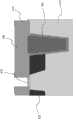
回到图4,图4图示已经在基板410上执行根据本方法的蚀刻工艺的基板410的横剖面图。在假栅极(未图示)的沉积之前,在基板410上沉积HDP质量的介电材料415。伴随着间隔物形成430执行蚀刻、浅沟槽隔离420与注入掺杂425。或者,可在HDP质量的介电材料与假栅极的沉积之前执行浅沟槽隔离420。在基板上沉积第二介电层或夹层电介质435,第二介电层或夹层电介质435在沉积之后最初可为可流动的,且执行CMP以移除过量的电介质并暴露假栅极。执行多晶硅选择性湿法蚀刻以移除假栅极,藉此暴露HDP质量的介电材料415。将三氟化氮、氨以及氦的干法蚀刻剂气体混合物暴露至基板,以移除HDP质量的介电材料415。在流入反应区之前,气体可流过远程等离子体腔室。可在HDP质量的介电材料415的移除过程中移除一数量的夹层电介质435。然而,即便夹层电介质435的质量可能低于HDP质量的介电材料415,干法蚀刻剂气体混合物可在实质上相似速率下移除层。因此,在HDP质量的介电材料的移除过程中限制被移除的夹层介电材料435的数量。Returning to FIG. 4 , FIG. 4 illustrates a cross-sectional view of a
示例example
在利用干法蚀刻剂气体混合物的蚀刻选择性之间作出比较示例。在包含藉由HDP CVD以及可流动CVD沉积的氧化物的基板上执行蚀刻。在蚀刻之前以400℃下的退火来固化可流动氧化物。将氧化物暴露至含有三氟化氮与氨的干法蚀刻剂气体混合物达十三秒的时间段。如下方表I中可见,干法蚀刻剂气体混合物仅移除稍微多一点的可流动氧化物(相较于HDP质量的氧化物),如此指出干法蚀刻剂气体实质上对氧化物质量不敏感:A comparative example was made between etch selectivities using dry etchant gas mixtures. Etching is performed on substrates containing oxides deposited by HDP CVD as well as flowable CVD. The flowable oxide was cured with an anneal at 400°C prior to etching. The oxide was exposed to a dry etchant gas mixture containing nitrogen trifluoride and ammonia for a period of thirteen seconds. As can be seen in Table I below, the dry etchant gas mixture removed only slightly more flowable oxide (compared to HDP quality oxide), thus indicating that the dry etchant gas is substantially insensitive to oxide quality :
表I:干法蚀刻剂气体的蚀刻深度Table I: Etch Depth of Dry Etchant Gases
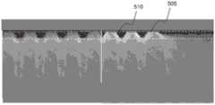
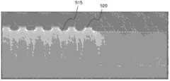
图5A是图示利用HF水溶液蚀刻剂的沟槽与开放区中的蚀刻深度的SEM图像。HF对氧化物质量敏感,因此氧化物质量中的差异反映在不同的蚀刻深度中。开放区505不具有均匀高度,且沟槽510显示不一致数量的氧化物移除。然而,图5B图标SEM图像,SEM图像显示利用干法蚀刻剂气体混合物的沟槽与开放区中的蚀刻深度。干法蚀刻剂气体混合物包括三氟化氮与氨。干法蚀刻剂气体混合物实质上对氧化物质量不敏感,且开放区520与沟槽515两者的凹陷数量是实质上相似与均匀的。FIG. 5A is a SEM image illustrating etch depths in trenches and open areas using HF aqueous etchant. HF is sensitive to oxide quality, so differences in oxide quality are reflected in different etch depths.
在先前描述中,为了说明,已经提出多个细节以提供本发明技术的多个实施例的理解。然而,熟悉技术人士可理解可在不具有这些细节的某些细节或具有额外细节下执行某些实施例。In the previous description, for purposes of explanation, numerous details have been set forth in order to provide an understanding of various embodiments of the inventive technology. However, one skilled in the art will understand that certain embodiments may be practiced without some of these details or with additional details.
已经揭露多个实施例,本领域技术人员可理解可在不悖离所揭露实施例的精神下应用多种修改、替换构造与等效物。此外,并未已经描述多种习知工艺与组件以避免非必要地模糊本发明。因此,上方描述不应被用来限制本发明的范围。Having disclosed several embodiments, it will be understood by those skilled in the art that various modifications, alternative constructions, and equivalents may be applied without departing from the spirit of the disclosed embodiments. Additionally, various well-known processes and components have not been described in order to avoid unnecessarily obscuring the present invention. Therefore, the above description should not be taken to limit the scope of the present invention.
值得注意的是,可将各个实施例描述成以流程图、流动图或框图绘制的工艺。虽然流程图可描述方法为依序工艺,但可并行或并发地执行多个操作。此外,可重新排列操作的次序。当工艺的操作完成时可终止工艺,但工艺可具有示图中未讨论或包含的额外步骤。再者,并非任何特定描述工艺中的所有操作会发生于所有实施例中。工艺可对应于方法、函数、程序、子例程、子程序等等。当工艺对应于函数时,工艺的终结对应于所述函数对调用函数或主函数的返回。It is worth noting that various embodiments may be described as processes drawn in flowcharts, flow diagrams, or block diagrams. Although a flowchart may describe a method as a sequential process, multiple operations may be performed in parallel or concurrently. Also, the order of operations may be rearranged. A process may be terminated when its operations are complete, but the process may have additional steps not discussed or included in the diagram. Furthermore, not all operations in any particular described process will occur in all embodiments. A process may correspond to a method, function, procedure, subroutine, subroutine, or the like. When a craft corresponds to a function, the termination of the craft corresponds to the return of said function to the calling or main function.
除非文中清楚地另外指出,否则当提供数值范围时,可理解此举亦明确揭露范围的上限与下限之间的各个中间值至下限单位的最小分数。包含声明范围中的任何声明数值或中间值以及所述声明范围中的任何其它声明数值或中间值之间的各个较小范围。根据声明范围中任何特定排除的界限,可在范围中独立地将那些较小范围的上限与下限包括或排除,且界限中的任一者、两者皆不被或两者皆被包含于较小范围中的每个范围亦包含于本发明中。当声明范围包括界限中的一者或两者时,亦包括排除那些所包含的界限中的一者或两者的范围。Unless the context clearly dictates otherwise, when a range of values is provided, it is understood that each intervening value between the upper and lower limits of the range, down to the smallest fraction of the unit of the lower limit, is also expressly disclosed. Each smaller range between any stated value or intervening value in a stated range and any other stated or intervening value in said stated range is encompassed. Subject to any specifically excluded limit in a stated range, the upper and lower limits of those smaller ranges may independently be included or excluded in the range, and either, neither, or both of the limits are included in the lesser range. Each of the smaller ranges is also encompassed in the invention. Where the stated range includes one or both of the limits, ranges excluding either or both of those included limits are also included.
除非文中清楚以其它方式指出,否则本文与所附权利要求书中所用的单数形式”一”、“一个”以及“所述”包括复数引用。因此,举例而言,对“介电材料”的引用包括多个此类材料,而对“所述沉积”的引用包括对一个或多个沉积以及本领域技术人员所习知的沉积等效物的引用等等。As used herein and in the appended claims, the singular forms "a," "an," and "the" include plural references unless the context clearly dictates otherwise. Thus, by way of example, reference to "a dielectric material" includes a plurality of such materials and reference to "the deposition" includes reference to one or more depositions and equivalent depositions known to those skilled in the art. citations etc.
再者,当用于本说明书与所附权利要求书中时,措辞“包括”、“包括有”、“包含”、和“包含有”旨在表明所声明特征、整数、部件或步骤的存在,但这些措辞并不排除一个或多个其它特征、整数、部件、步骤、行为或群组的存在或添加。Furthermore, when used in this specification and the appended claims, the words "comprises", "includes", "comprises", and "comprises" are intended to indicate the presence of stated features, integers, components or steps , but these terms do not exclude the presence or addition of one or more other features, integers, components, steps, acts or groups.
Claims (19)
Translated fromChineseApplications Claiming Priority (5)
| Application Number | Priority Date | Filing Date | Title |
|---|---|---|---|
| US201161539270P | 2011-09-26 | 2011-09-26 | |
| US61/539,270 | 2011-09-26 | ||
| US13/624,693US20130260564A1 (en) | 2011-09-26 | 2012-09-21 | Insensitive dry removal process for semiconductor integration |
| US13/624,693 | 2012-09-21 | ||
| PCT/US2012/057358WO2013049223A2 (en) | 2011-09-26 | 2012-09-26 | Insensitive dry removal process for semiconductor integration |
Publications (1)
| Publication Number | Publication Date |
|---|---|
| CN103843118Atrue CN103843118A (en) | 2014-06-04 |
Family
ID=47996724
Family Applications (1)
| Application Number | Title | Priority Date | Filing Date |
|---|---|---|---|
| CN201280048556.7APendingCN103843118A (en) | 2011-09-26 | 2012-09-26 | Insensitive dry removal process for semiconductor integration |
Country Status (6)
| Country | Link |
|---|---|
| US (1) | US20130260564A1 (en) |
| JP (1) | JP2014527315A (en) |
| KR (1) | KR20140070630A (en) |
| CN (1) | CN103843118A (en) |
| TW (1) | TWI541898B (en) |
| WO (1) | WO2013049223A2 (en) |
Families Citing this family (131)
| Publication number | Priority date | Publication date | Assignee | Title |
|---|---|---|---|---|
| US9324576B2 (en) | 2010-05-27 | 2016-04-26 | Applied Materials, Inc. | Selective etch for silicon films |
| US10283321B2 (en) | 2011-01-18 | 2019-05-07 | Applied Materials, Inc. | Semiconductor processing system and methods using capacitively coupled plasma |
| US9064815B2 (en) | 2011-03-14 | 2015-06-23 | Applied Materials, Inc. | Methods for etch of metal and metal-oxide films |
| US8999856B2 (en) | 2011-03-14 | 2015-04-07 | Applied Materials, Inc. | Methods for etch of sin films |
| US8808563B2 (en) | 2011-10-07 | 2014-08-19 | Applied Materials, Inc. | Selective etch of silicon by way of metastable hydrogen termination |
| US9267739B2 (en) | 2012-07-18 | 2016-02-23 | Applied Materials, Inc. | Pedestal with multi-zone temperature control and multiple purge capabilities |
| US9373517B2 (en) | 2012-08-02 | 2016-06-21 | Applied Materials, Inc. | Semiconductor processing with DC assisted RF power for improved control |
| US9034770B2 (en) | 2012-09-17 | 2015-05-19 | Applied Materials, Inc. | Differential silicon oxide etch |
| US9023734B2 (en) | 2012-09-18 | 2015-05-05 | Applied Materials, Inc. | Radical-component oxide etch |
| US9390937B2 (en) | 2012-09-20 | 2016-07-12 | Applied Materials, Inc. | Silicon-carbon-nitride selective etch |
| US9132436B2 (en) | 2012-09-21 | 2015-09-15 | Applied Materials, Inc. | Chemical control features in wafer process equipment |
| US8969212B2 (en) | 2012-11-20 | 2015-03-03 | Applied Materials, Inc. | Dry-etch selectivity |
| US8980763B2 (en) | 2012-11-30 | 2015-03-17 | Applied Materials, Inc. | Dry-etch for selective tungsten removal |
| US9111877B2 (en) | 2012-12-18 | 2015-08-18 | Applied Materials, Inc. | Non-local plasma oxide etch |
| US8921234B2 (en) | 2012-12-21 | 2014-12-30 | Applied Materials, Inc. | Selective titanium nitride etching |
| US10256079B2 (en) | 2013-02-08 | 2019-04-09 | Applied Materials, Inc. | Semiconductor processing systems having multiple plasma configurations |
| US9362130B2 (en) | 2013-03-01 | 2016-06-07 | Applied Materials, Inc. | Enhanced etching processes using remote plasma sources |
| US8921235B2 (en)* | 2013-03-04 | 2014-12-30 | Applied Materials, Inc. | Controlled air gap formation |
| US9040422B2 (en) | 2013-03-05 | 2015-05-26 | Applied Materials, Inc. | Selective titanium nitride removal |
| US20140271097A1 (en) | 2013-03-15 | 2014-09-18 | Applied Materials, Inc. | Processing systems and methods for halide scavenging |
| US9493879B2 (en) | 2013-07-12 | 2016-11-15 | Applied Materials, Inc. | Selective sputtering for pattern transfer |
| US9773648B2 (en) | 2013-08-30 | 2017-09-26 | Applied Materials, Inc. | Dual discharge modes operation for remote plasma |
| US9576809B2 (en) | 2013-11-04 | 2017-02-21 | Applied Materials, Inc. | Etch suppression with germanium |
| US9520303B2 (en) | 2013-11-12 | 2016-12-13 | Applied Materials, Inc. | Aluminum selective etch |
| US9245762B2 (en) | 2013-12-02 | 2016-01-26 | Applied Materials, Inc. | Procedure for etch rate consistency |
| US9287095B2 (en) | 2013-12-17 | 2016-03-15 | Applied Materials, Inc. | Semiconductor system assemblies and methods of operation |
| US9287134B2 (en) | 2014-01-17 | 2016-03-15 | Applied Materials, Inc. | Titanium oxide etch |
| US20150206803A1 (en)* | 2014-01-19 | 2015-07-23 | United Microelectronics Corp. | Method of forming inter-level dielectric layer |
| US9396989B2 (en) | 2014-01-27 | 2016-07-19 | Applied Materials, Inc. | Air gaps between copper lines |
| US9293568B2 (en) | 2014-01-27 | 2016-03-22 | Applied Materials, Inc. | Method of fin patterning |
| US9385028B2 (en) | 2014-02-03 | 2016-07-05 | Applied Materials, Inc. | Air gap process |
| US9499898B2 (en) | 2014-03-03 | 2016-11-22 | Applied Materials, Inc. | Layered thin film heater and method of fabrication |
| US9299575B2 (en) | 2014-03-17 | 2016-03-29 | Applied Materials, Inc. | Gas-phase tungsten etch |
| US9299537B2 (en) | 2014-03-20 | 2016-03-29 | Applied Materials, Inc. | Radial waveguide systems and methods for post-match control of microwaves |
| US9299538B2 (en) | 2014-03-20 | 2016-03-29 | Applied Materials, Inc. | Radial waveguide systems and methods for post-match control of microwaves |
| US9903020B2 (en) | 2014-03-31 | 2018-02-27 | Applied Materials, Inc. | Generation of compact alumina passivation layers on aluminum plasma equipment components |
| US9269590B2 (en) | 2014-04-07 | 2016-02-23 | Applied Materials, Inc. | Spacer formation |
| US9309598B2 (en) | 2014-05-28 | 2016-04-12 | Applied Materials, Inc. | Oxide and metal removal |
| US9378969B2 (en) | 2014-06-19 | 2016-06-28 | Applied Materials, Inc. | Low temperature gas-phase carbon removal |
| US9406523B2 (en) | 2014-06-19 | 2016-08-02 | Applied Materials, Inc. | Highly selective doped oxide removal method |
| US9425058B2 (en) | 2014-07-24 | 2016-08-23 | Applied Materials, Inc. | Simplified litho-etch-litho-etch process |
| US9378978B2 (en) | 2014-07-31 | 2016-06-28 | Applied Materials, Inc. | Integrated oxide recess and floating gate fin trimming |
| US9496167B2 (en) | 2014-07-31 | 2016-11-15 | Applied Materials, Inc. | Integrated bit-line airgap formation and gate stack post clean |
| US9659753B2 (en) | 2014-08-07 | 2017-05-23 | Applied Materials, Inc. | Grooved insulator to reduce leakage current |
| US9553102B2 (en) | 2014-08-19 | 2017-01-24 | Applied Materials, Inc. | Tungsten separation |
| US9355856B2 (en) | 2014-09-12 | 2016-05-31 | Applied Materials, Inc. | V trench dry etch |
| US9368364B2 (en) | 2014-09-24 | 2016-06-14 | Applied Materials, Inc. | Silicon etch process with tunable selectivity to SiO2 and other materials |
| US9355862B2 (en) | 2014-09-24 | 2016-05-31 | Applied Materials, Inc. | Fluorine-based hardmask removal |
| US9613822B2 (en) | 2014-09-25 | 2017-04-04 | Applied Materials, Inc. | Oxide etch selectivity enhancement |
| US9355922B2 (en) | 2014-10-14 | 2016-05-31 | Applied Materials, Inc. | Systems and methods for internal surface conditioning in plasma processing equipment |
| US9966240B2 (en) | 2014-10-14 | 2018-05-08 | Applied Materials, Inc. | Systems and methods for internal surface conditioning assessment in plasma processing equipment |
| US11637002B2 (en) | 2014-11-26 | 2023-04-25 | Applied Materials, Inc. | Methods and systems to enhance process uniformity |
| US9299583B1 (en) | 2014-12-05 | 2016-03-29 | Applied Materials, Inc. | Aluminum oxide selective etch |
| US10224210B2 (en) | 2014-12-09 | 2019-03-05 | Applied Materials, Inc. | Plasma processing system with direct outlet toroidal plasma source |
| US10573496B2 (en) | 2014-12-09 | 2020-02-25 | Applied Materials, Inc. | Direct outlet toroidal plasma source |
| US9502258B2 (en) | 2014-12-23 | 2016-11-22 | Applied Materials, Inc. | Anisotropic gap etch |
| US9343272B1 (en) | 2015-01-08 | 2016-05-17 | Applied Materials, Inc. | Self-aligned process |
| US11257693B2 (en) | 2015-01-09 | 2022-02-22 | Applied Materials, Inc. | Methods and systems to improve pedestal temperature control |
| US9373522B1 (en) | 2015-01-22 | 2016-06-21 | Applied Mateials, Inc. | Titanium nitride removal |
| US9449846B2 (en) | 2015-01-28 | 2016-09-20 | Applied Materials, Inc. | Vertical gate separation |
| US20160225652A1 (en) | 2015-02-03 | 2016-08-04 | Applied Materials, Inc. | Low temperature chuck for plasma processing systems |
| US9728437B2 (en) | 2015-02-03 | 2017-08-08 | Applied Materials, Inc. | High temperature chuck for plasma processing systems |
| US9881805B2 (en) | 2015-03-02 | 2018-01-30 | Applied Materials, Inc. | Silicon selective removal |
| JP6434367B2 (en)* | 2015-05-14 | 2018-12-05 | 東京エレクトロン株式会社 | Substrate liquid processing apparatus, substrate liquid processing method, and computer readable storage medium storing substrate liquid processing program |
| US9691645B2 (en) | 2015-08-06 | 2017-06-27 | Applied Materials, Inc. | Bolted wafer chuck thermal management systems and methods for wafer processing systems |
| US9741593B2 (en) | 2015-08-06 | 2017-08-22 | Applied Materials, Inc. | Thermal management systems and methods for wafer processing systems |
| US9349605B1 (en) | 2015-08-07 | 2016-05-24 | Applied Materials, Inc. | Oxide etch selectivity systems and methods |
| US10504700B2 (en) | 2015-08-27 | 2019-12-10 | Applied Materials, Inc. | Plasma etching systems and methods with secondary plasma injection |
| US10504754B2 (en) | 2016-05-19 | 2019-12-10 | Applied Materials, Inc. | Systems and methods for improved semiconductor etching and component protection |
| US10522371B2 (en) | 2016-05-19 | 2019-12-31 | Applied Materials, Inc. | Systems and methods for improved semiconductor etching and component protection |
| US9865484B1 (en) | 2016-06-29 | 2018-01-09 | Applied Materials, Inc. | Selective etch using material modification and RF pulsing |
| US10062575B2 (en) | 2016-09-09 | 2018-08-28 | Applied Materials, Inc. | Poly directional etch by oxidation |
| US10629473B2 (en) | 2016-09-09 | 2020-04-21 | Applied Materials, Inc. | Footing removal for nitride spacer |
| US9721789B1 (en) | 2016-10-04 | 2017-08-01 | Applied Materials, Inc. | Saving ion-damaged spacers |
| US9934942B1 (en) | 2016-10-04 | 2018-04-03 | Applied Materials, Inc. | Chamber with flow-through source |
| US10062585B2 (en) | 2016-10-04 | 2018-08-28 | Applied Materials, Inc. | Oxygen compatible plasma source |
| US10546729B2 (en) | 2016-10-04 | 2020-01-28 | Applied Materials, Inc. | Dual-channel showerhead with improved profile |
| US10062579B2 (en) | 2016-10-07 | 2018-08-28 | Applied Materials, Inc. | Selective SiN lateral recess |
| US9947549B1 (en) | 2016-10-10 | 2018-04-17 | Applied Materials, Inc. | Cobalt-containing material removal |
| US9768034B1 (en) | 2016-11-11 | 2017-09-19 | Applied Materials, Inc. | Removal methods for high aspect ratio structures |
| US10163696B2 (en) | 2016-11-11 | 2018-12-25 | Applied Materials, Inc. | Selective cobalt removal for bottom up gapfill |
| US10242908B2 (en) | 2016-11-14 | 2019-03-26 | Applied Materials, Inc. | Airgap formation with damage-free copper |
| US10026621B2 (en) | 2016-11-14 | 2018-07-17 | Applied Materials, Inc. | SiN spacer profile patterning |
| US10566206B2 (en) | 2016-12-27 | 2020-02-18 | Applied Materials, Inc. | Systems and methods for anisotropic material breakthrough |
| US10431429B2 (en) | 2017-02-03 | 2019-10-01 | Applied Materials, Inc. | Systems and methods for radial and azimuthal control of plasma uniformity |
| US10403507B2 (en) | 2017-02-03 | 2019-09-03 | Applied Materials, Inc. | Shaped etch profile with oxidation |
| US10043684B1 (en) | 2017-02-06 | 2018-08-07 | Applied Materials, Inc. | Self-limiting atomic thermal etching systems and methods |
| US10319739B2 (en) | 2017-02-08 | 2019-06-11 | Applied Materials, Inc. | Accommodating imperfectly aligned memory holes |
| US10943834B2 (en) | 2017-03-13 | 2021-03-09 | Applied Materials, Inc. | Replacement contact process |
| US10319649B2 (en) | 2017-04-11 | 2019-06-11 | Applied Materials, Inc. | Optical emission spectroscopy (OES) for remote plasma monitoring |
| JP7176860B6 (en) | 2017-05-17 | 2022-12-16 | アプライド マテリアルズ インコーポレイテッド | Semiconductor processing chamber to improve precursor flow |
| US11276590B2 (en) | 2017-05-17 | 2022-03-15 | Applied Materials, Inc. | Multi-zone semiconductor substrate supports |
| US11276559B2 (en) | 2017-05-17 | 2022-03-15 | Applied Materials, Inc. | Semiconductor processing chamber for multiple precursor flow |
| US10049891B1 (en) | 2017-05-31 | 2018-08-14 | Applied Materials, Inc. | Selective in situ cobalt residue removal |
| US10497579B2 (en) | 2017-05-31 | 2019-12-03 | Applied Materials, Inc. | Water-free etching methods |
| US10920320B2 (en) | 2017-06-16 | 2021-02-16 | Applied Materials, Inc. | Plasma health determination in semiconductor substrate processing reactors |
| US10541246B2 (en) | 2017-06-26 | 2020-01-21 | Applied Materials, Inc. | 3D flash memory cells which discourage cross-cell electrical tunneling |
| US10727080B2 (en) | 2017-07-07 | 2020-07-28 | Applied Materials, Inc. | Tantalum-containing material removal |
| US10541184B2 (en) | 2017-07-11 | 2020-01-21 | Applied Materials, Inc. | Optical emission spectroscopic techniques for monitoring etching |
| US10354889B2 (en) | 2017-07-17 | 2019-07-16 | Applied Materials, Inc. | Non-halogen etching of silicon-containing materials |
| US10170336B1 (en) | 2017-08-04 | 2019-01-01 | Applied Materials, Inc. | Methods for anisotropic control of selective silicon removal |
| US10043674B1 (en) | 2017-08-04 | 2018-08-07 | Applied Materials, Inc. | Germanium etching systems and methods |
| US10297458B2 (en) | 2017-08-07 | 2019-05-21 | Applied Materials, Inc. | Process window widening using coated parts in plasma etch processes |
| US10128086B1 (en) | 2017-10-24 | 2018-11-13 | Applied Materials, Inc. | Silicon pretreatment for nitride removal |
| US10283324B1 (en) | 2017-10-24 | 2019-05-07 | Applied Materials, Inc. | Oxygen treatment for nitride etching |
| US10256112B1 (en) | 2017-12-08 | 2019-04-09 | Applied Materials, Inc. | Selective tungsten removal |
| US10903054B2 (en) | 2017-12-19 | 2021-01-26 | Applied Materials, Inc. | Multi-zone gas distribution systems and methods |
| US11328909B2 (en) | 2017-12-22 | 2022-05-10 | Applied Materials, Inc. | Chamber conditioning and removal processes |
| US10854426B2 (en) | 2018-01-08 | 2020-12-01 | Applied Materials, Inc. | Metal recess for semiconductor structures |
| US10679870B2 (en) | 2018-02-15 | 2020-06-09 | Applied Materials, Inc. | Semiconductor processing chamber multistage mixing apparatus |
| US10964512B2 (en) | 2018-02-15 | 2021-03-30 | Applied Materials, Inc. | Semiconductor processing chamber multistage mixing apparatus and methods |
| TWI766433B (en) | 2018-02-28 | 2022-06-01 | 美商應用材料股份有限公司 | Systems and methods to form airgaps |
| US10593560B2 (en) | 2018-03-01 | 2020-03-17 | Applied Materials, Inc. | Magnetic induction plasma source for semiconductor processes and equipment |
| US10319600B1 (en) | 2018-03-12 | 2019-06-11 | Applied Materials, Inc. | Thermal silicon etch |
| US10497573B2 (en) | 2018-03-13 | 2019-12-03 | Applied Materials, Inc. | Selective atomic layer etching of semiconductor materials |
| US10573527B2 (en) | 2018-04-06 | 2020-02-25 | Applied Materials, Inc. | Gas-phase selective etching systems and methods |
| US10490406B2 (en) | 2018-04-10 | 2019-11-26 | Appled Materials, Inc. | Systems and methods for material breakthrough |
| US10699879B2 (en) | 2018-04-17 | 2020-06-30 | Applied Materials, Inc. | Two piece electrode assembly with gap for plasma control |
| US10886137B2 (en) | 2018-04-30 | 2021-01-05 | Applied Materials, Inc. | Selective nitride removal |
| US10872778B2 (en) | 2018-07-06 | 2020-12-22 | Applied Materials, Inc. | Systems and methods utilizing solid-phase etchants |
| US10755941B2 (en) | 2018-07-06 | 2020-08-25 | Applied Materials, Inc. | Self-limiting selective etching systems and methods |
| US10672642B2 (en) | 2018-07-24 | 2020-06-02 | Applied Materials, Inc. | Systems and methods for pedestal configuration |
| US10892198B2 (en) | 2018-09-14 | 2021-01-12 | Applied Materials, Inc. | Systems and methods for improved performance in semiconductor processing |
| US11049755B2 (en) | 2018-09-14 | 2021-06-29 | Applied Materials, Inc. | Semiconductor substrate supports with embedded RF shield |
| US11062887B2 (en) | 2018-09-17 | 2021-07-13 | Applied Materials, Inc. | High temperature RF heater pedestals |
| US11417534B2 (en) | 2018-09-21 | 2022-08-16 | Applied Materials, Inc. | Selective material removal |
| US11682560B2 (en) | 2018-10-11 | 2023-06-20 | Applied Materials, Inc. | Systems and methods for hafnium-containing film removal |
| US11121002B2 (en) | 2018-10-24 | 2021-09-14 | Applied Materials, Inc. | Systems and methods for etching metals and metal derivatives |
| US11437242B2 (en) | 2018-11-27 | 2022-09-06 | Applied Materials, Inc. | Selective removal of silicon-containing materials |
| US11721527B2 (en) | 2019-01-07 | 2023-08-08 | Applied Materials, Inc. | Processing chamber mixing systems |
| US10920319B2 (en) | 2019-01-11 | 2021-02-16 | Applied Materials, Inc. | Ceramic showerheads with conductive electrodes |
Family Cites Families (28)
| Publication number | Priority date | Publication date | Assignee | Title |
|---|---|---|---|---|
| US5300463A (en)* | 1992-03-06 | 1994-04-05 | Micron Technology, Inc. | Method of selectively etching silicon dioxide dielectric layers on semiconductor wafers |
| JP3330554B2 (en)* | 1999-01-27 | 2002-09-30 | 松下電器産業株式会社 | Etching method |
| US6291282B1 (en)* | 1999-02-26 | 2001-09-18 | Texas Instruments Incorporated | Method of forming dual metal gate structures or CMOS devices |
| KR100350056B1 (en)* | 2000-03-09 | 2002-08-24 | 삼성전자 주식회사 | Method of forming a self-aligned contact pad in a damascene gate process |
| US6303418B1 (en)* | 2000-06-30 | 2001-10-16 | Chartered Semiconductor Manufacturing Ltd. | Method of fabricating CMOS devices featuring dual gate structures and a high dielectric constant gate insulator layer |
| KR100484258B1 (en)* | 2001-12-27 | 2005-04-22 | 주식회사 하이닉스반도체 | Method for fabricating semiconductor device |
| US7582555B1 (en)* | 2005-12-29 | 2009-09-01 | Novellus Systems, Inc. | CVD flowable gap fill |
| US20050272191A1 (en)* | 2004-06-03 | 2005-12-08 | Uday Shah | Replacement gate process for making a semiconductor device that includes a metal gate electrode |
| KR100703014B1 (en)* | 2005-10-26 | 2007-04-06 | 삼성전자주식회사 | Silicon oxide etchant and method for manufacturing semiconductor device using same |
| US20070281106A1 (en)* | 2006-05-30 | 2007-12-06 | Applied Materials, Inc. | Process chamber for dielectric gapfill |
| KR100818708B1 (en)* | 2006-08-18 | 2008-04-01 | 주식회사 하이닉스반도체 | Method of manufacturing semiconductor device including surface cleaning |
| US8110787B1 (en)* | 2006-08-23 | 2012-02-07 | ON Semiconductor Trading, Ltd | Image sensor with a reflective waveguide |
| WO2008074672A1 (en)* | 2006-12-20 | 2008-06-26 | Nxp B.V. | Improving adhesion of diffusion barrier on cu containing interconnect element |
| JP5282419B2 (en)* | 2007-04-18 | 2013-09-04 | ソニー株式会社 | Semiconductor device and manufacturing method thereof |
| KR100877107B1 (en)* | 2007-06-28 | 2009-01-07 | 주식회사 하이닉스반도체 | Method of forming interlayer insulating film of semiconductor device |
| TW200933812A (en)* | 2008-01-30 | 2009-08-01 | Promos Technologies Inc | Process for forming trench isolation structure and semiconductor device produced thereby |
| US8357435B2 (en)* | 2008-05-09 | 2013-01-22 | Applied Materials, Inc. | Flowable dielectric equipment and processes |
| US7910491B2 (en)* | 2008-10-16 | 2011-03-22 | Applied Materials, Inc. | Gapfill improvement with low etch rate dielectric liners |
| WO2011072143A2 (en)* | 2009-12-09 | 2011-06-16 | Novellus Systems, Inc. | Novel gap fill integration |
| US20110151677A1 (en)* | 2009-12-21 | 2011-06-23 | Applied Materials, Inc. | Wet oxidation process performed on a dielectric material formed from a flowable cvd process |
| US8501629B2 (en)* | 2009-12-23 | 2013-08-06 | Applied Materials, Inc. | Smooth SiConi etch for silicon-containing films |
| US8361338B2 (en)* | 2010-02-11 | 2013-01-29 | Taiwan Semiconductor Manufacturing Company, Ltd. | Hard mask removal method |
| US8535998B2 (en)* | 2010-03-09 | 2013-09-17 | Taiwan Semiconductor Manufacturing Company, Ltd. | Method for fabricating a gate structure |
| US8475674B2 (en)* | 2010-04-30 | 2013-07-02 | Applied Materials, Inc. | High-temperature selective dry etch having reduced post-etch solid residue |
| KR20120058962A (en)* | 2010-11-30 | 2012-06-08 | 삼성전자주식회사 | Fabricating method of semiconductor device |
| US8415250B2 (en)* | 2011-04-29 | 2013-04-09 | International Business Machines Corporation | Method of forming silicide contacts of different shapes selectively on regions of a semiconductor device |
| US9012283B2 (en)* | 2011-05-16 | 2015-04-21 | International Business Machines Corporation | Integrated circuit (IC) chip having both metal and silicon gate field effect transistors (FETs) and method of manufacture |
| US8927390B2 (en)* | 2011-09-26 | 2015-01-06 | Applied Materials, Inc. | Intrench profile |
- 2012
- 2012-09-21USUS13/624,693patent/US20130260564A1/ennot_activeAbandoned
- 2012-09-26CNCN201280048556.7Apatent/CN103843118A/enactivePending
- 2012-09-26KRKR1020147011222Apatent/KR20140070630A/ennot_activeWithdrawn
- 2012-09-26WOPCT/US2012/057358patent/WO2013049223A2/enactiveApplication Filing
- 2012-09-26TWTW101135392Apatent/TWI541898B/ennot_activeIP Right Cessation
- 2012-09-26JPJP2014532110Apatent/JP2014527315A/enactivePending
Also Published As
| Publication number | Publication date |
|---|---|
| KR20140070630A (en) | 2014-06-10 |
| US20130260564A1 (en) | 2013-10-03 |
| WO2013049223A2 (en) | 2013-04-04 |
| WO2013049223A3 (en) | 2013-05-23 |
| TW201330101A (en) | 2013-07-16 |
| JP2014527315A (en) | 2014-10-09 |
| TWI541898B (en) | 2016-07-11 |
Similar Documents
| Publication | Publication Date | Title |
|---|---|---|
| CN103843118A (en) | Insensitive dry removal process for semiconductor integration | |
| CN103907182B (en) | The groove Internal periphery of improvement | |
| US11515149B2 (en) | Deposition of flowable silicon-containing films | |
| CN100452318C (en) | Method for producing gate stack sidewall spacers | |
| KR101161098B1 (en) | Gapfill improvement with low etch rate dielectric liners | |
| TWI479044B (en) | Boron film interface engineering | |
| JP6856651B2 (en) | Nanowire Manufacturing Methods for Horizontal Gate All-Around Devices for Semiconductor Applications | |
| CN101743631B (en) | Boron derived materials deposition method | |
| KR20100038311A (en) | Boron nitride and boron nitride-derived materials deposition method | |
| EP1913629A1 (en) | Method of forming a high dielectric constant film and method of forming a semiconductor device | |
| JP2020516079A (en) | Two-step process for silicon gap filling | |
| US9312167B1 (en) | Air-gap structure formation with ultra low-k dielectric layer on PECVD low-k chamber | |
| KR101008490B1 (en) | Oxide film deposition method by low temperature chemical vapor deposition | |
| KR20240024026A (en) | Substrate processing method | |
| JP2007204851A (en) | Method for producing semiconductor device |
Legal Events
| Date | Code | Title | Description |
|---|---|---|---|
| C06 | Publication | ||
| PB01 | Publication | ||
| C02 | Deemed withdrawal of patent application after publication (patent law 2001) | ||
| WD01 | Invention patent application deemed withdrawn after publication | Application publication date:20140604 |