CN103811503A - Array substrate and preparation method and display panel - Google Patents
Array substrate and preparation method and display panelDownload PDFInfo
- Publication number
- CN103811503A CN103811503ACN201410057337.6ACN201410057337ACN103811503ACN 103811503 ACN103811503 ACN 103811503ACN 201410057337 ACN201410057337 ACN 201410057337ACN 103811503 ACN103811503 ACN 103811503A
- Authority
- CN
- China
- Prior art keywords
- thin film
- film transistor
- oxide thin
- drain
- patterning process
- Prior art date
- Legal status (The legal status is an assumption and is not a legal conclusion. Google has not performed a legal analysis and makes no representation as to the accuracy of the status listed.)
- Pending
Links
Images


Classifications
- G—PHYSICS
- G02—OPTICS
- G02F—OPTICAL DEVICES OR ARRANGEMENTS FOR THE CONTROL OF LIGHT BY MODIFICATION OF THE OPTICAL PROPERTIES OF THE MEDIA OF THE ELEMENTS INVOLVED THEREIN; NON-LINEAR OPTICS; FREQUENCY-CHANGING OF LIGHT; OPTICAL LOGIC ELEMENTS; OPTICAL ANALOGUE/DIGITAL CONVERTERS
- G02F1/00—Devices or arrangements for the control of the intensity, colour, phase, polarisation or direction of light arriving from an independent light source, e.g. switching, gating or modulating; Non-linear optics
- G02F1/01—Devices or arrangements for the control of the intensity, colour, phase, polarisation or direction of light arriving from an independent light source, e.g. switching, gating or modulating; Non-linear optics for the control of the intensity, phase, polarisation or colour
- G02F1/13—Devices or arrangements for the control of the intensity, colour, phase, polarisation or direction of light arriving from an independent light source, e.g. switching, gating or modulating; Non-linear optics for the control of the intensity, phase, polarisation or colour based on liquid crystals, e.g. single liquid crystal display cells
- G02F1/133—Constructional arrangements; Operation of liquid crystal cells; Circuit arrangements
- G02F1/136—Liquid crystal cells structurally associated with a semi-conducting layer or substrate, e.g. cells forming part of an integrated circuit
- G02F1/1362—Active matrix addressed cells
- G02F1/13624—Active matrix addressed cells having more than one switching element per pixel
- H—ELECTRICITY
- H01—ELECTRIC ELEMENTS
- H01L—SEMICONDUCTOR DEVICES NOT COVERED BY CLASS H10
- H01L21/00—Processes or apparatus adapted for the manufacture or treatment of semiconductor or solid state devices or of parts thereof
- H01L21/70—Manufacture or treatment of devices consisting of a plurality of solid state components formed in or on a common substrate or of parts thereof; Manufacture of integrated circuit devices or of parts thereof
- H01L21/77—Manufacture or treatment of devices consisting of a plurality of solid state components or integrated circuits formed in, or on, a common substrate
- H—ELECTRICITY
- H10—SEMICONDUCTOR DEVICES; ELECTRIC SOLID-STATE DEVICES NOT OTHERWISE PROVIDED FOR
- H10D—INORGANIC ELECTRIC SEMICONDUCTOR DEVICES
- H10D30/00—Field-effect transistors [FET]
- H10D30/01—Manufacture or treatment
- H10D30/021—Manufacture or treatment of FETs having insulated gates [IGFET]
- H10D30/031—Manufacture or treatment of FETs having insulated gates [IGFET] of thin-film transistors [TFT]
- H10D30/0312—Manufacture or treatment of FETs having insulated gates [IGFET] of thin-film transistors [TFT] characterised by the gate electrodes
- H10D30/0316—Manufacture or treatment of FETs having insulated gates [IGFET] of thin-film transistors [TFT] characterised by the gate electrodes of lateral bottom-gate TFTs comprising only a single gate
- H—ELECTRICITY
- H10—SEMICONDUCTOR DEVICES; ELECTRIC SOLID-STATE DEVICES NOT OTHERWISE PROVIDED FOR
- H10D—INORGANIC ELECTRIC SEMICONDUCTOR DEVICES
- H10D30/00—Field-effect transistors [FET]
- H10D30/01—Manufacture or treatment
- H10D30/021—Manufacture or treatment of FETs having insulated gates [IGFET]
- H10D30/031—Manufacture or treatment of FETs having insulated gates [IGFET] of thin-film transistors [TFT]
- H10D30/0321—Manufacture or treatment of FETs having insulated gates [IGFET] of thin-film transistors [TFT] comprising silicon, e.g. amorphous silicon or polysilicon
- H—ELECTRICITY
- H10—SEMICONDUCTOR DEVICES; ELECTRIC SOLID-STATE DEVICES NOT OTHERWISE PROVIDED FOR
- H10D—INORGANIC ELECTRIC SEMICONDUCTOR DEVICES
- H10D30/00—Field-effect transistors [FET]
- H10D30/60—Insulated-gate field-effect transistors [IGFET]
- H10D30/67—Thin-film transistors [TFT]
- H—ELECTRICITY
- H10—SEMICONDUCTOR DEVICES; ELECTRIC SOLID-STATE DEVICES NOT OTHERWISE PROVIDED FOR
- H10D—INORGANIC ELECTRIC SEMICONDUCTOR DEVICES
- H10D30/00—Field-effect transistors [FET]
- H10D30/60—Insulated-gate field-effect transistors [IGFET]
- H10D30/67—Thin-film transistors [TFT]
- H10D30/6729—Thin-film transistors [TFT] characterised by the electrodes
- H10D30/673—Thin-film transistors [TFT] characterised by the electrodes characterised by the shapes, relative sizes or dispositions of the gate electrodes
- H10D30/6732—Bottom-gate only TFTs
- H—ELECTRICITY
- H10—SEMICONDUCTOR DEVICES; ELECTRIC SOLID-STATE DEVICES NOT OTHERWISE PROVIDED FOR
- H10D—INORGANIC ELECTRIC SEMICONDUCTOR DEVICES
- H10D30/00—Field-effect transistors [FET]
- H10D30/60—Insulated-gate field-effect transistors [IGFET]
- H10D30/67—Thin-film transistors [TFT]
- H10D30/674—Thin-film transistors [TFT] characterised by the active materials
- H10D30/6741—Group IV materials, e.g. germanium or silicon carbide
- H10D30/6743—Silicon
- H10D30/6745—Polycrystalline or microcrystalline silicon
- H—ELECTRICITY
- H10—SEMICONDUCTOR DEVICES; ELECTRIC SOLID-STATE DEVICES NOT OTHERWISE PROVIDED FOR
- H10D—INORGANIC ELECTRIC SEMICONDUCTOR DEVICES
- H10D30/00—Field-effect transistors [FET]
- H10D30/60—Insulated-gate field-effect transistors [IGFET]
- H10D30/67—Thin-film transistors [TFT]
- H10D30/674—Thin-film transistors [TFT] characterised by the active materials
- H10D30/6755—Oxide semiconductors, e.g. zinc oxide, copper aluminium oxide or cadmium stannate
- H—ELECTRICITY
- H10—SEMICONDUCTOR DEVICES; ELECTRIC SOLID-STATE DEVICES NOT OTHERWISE PROVIDED FOR
- H10D—INORGANIC ELECTRIC SEMICONDUCTOR DEVICES
- H10D62/00—Semiconductor bodies, or regions thereof, of devices having potential barriers
- H10D62/40—Crystalline structures
- H—ELECTRICITY
- H10—SEMICONDUCTOR DEVICES; ELECTRIC SOLID-STATE DEVICES NOT OTHERWISE PROVIDED FOR
- H10D—INORGANIC ELECTRIC SEMICONDUCTOR DEVICES
- H10D62/00—Semiconductor bodies, or regions thereof, of devices having potential barriers
- H10D62/80—Semiconductor bodies, or regions thereof, of devices having potential barriers characterised by the materials
- H10D62/83—Semiconductor bodies, or regions thereof, of devices having potential barriers characterised by the materials being Group IV materials, e.g. B-doped Si or undoped Ge
- H—ELECTRICITY
- H10—SEMICONDUCTOR DEVICES; ELECTRIC SOLID-STATE DEVICES NOT OTHERWISE PROVIDED FOR
- H10D—INORGANIC ELECTRIC SEMICONDUCTOR DEVICES
- H10D62/00—Semiconductor bodies, or regions thereof, of devices having potential barriers
- H10D62/80—Semiconductor bodies, or regions thereof, of devices having potential barriers characterised by the materials
- H10D62/86—Semiconductor bodies, or regions thereof, of devices having potential barriers characterised by the materials being Group II-VI materials, e.g. ZnO
- H—ELECTRICITY
- H10—SEMICONDUCTOR DEVICES; ELECTRIC SOLID-STATE DEVICES NOT OTHERWISE PROVIDED FOR
- H10D—INORGANIC ELECTRIC SEMICONDUCTOR DEVICES
- H10D86/00—Integrated devices formed in or on insulating or conducting substrates, e.g. formed in silicon-on-insulator [SOI] substrates or on stainless steel or glass substrates
- H10D86/01—Manufacture or treatment
- H10D86/021—Manufacture or treatment of multiple TFTs
- H10D86/0231—Manufacture or treatment of multiple TFTs using masks, e.g. half-tone masks
- H—ELECTRICITY
- H10—SEMICONDUCTOR DEVICES; ELECTRIC SOLID-STATE DEVICES NOT OTHERWISE PROVIDED FOR
- H10D—INORGANIC ELECTRIC SEMICONDUCTOR DEVICES
- H10D86/00—Integrated devices formed in or on insulating or conducting substrates, e.g. formed in silicon-on-insulator [SOI] substrates or on stainless steel or glass substrates
- H10D86/40—Integrated devices formed in or on insulating or conducting substrates, e.g. formed in silicon-on-insulator [SOI] substrates or on stainless steel or glass substrates characterised by multiple TFTs
- H10D86/421—Integrated devices formed in or on insulating or conducting substrates, e.g. formed in silicon-on-insulator [SOI] substrates or on stainless steel or glass substrates characterised by multiple TFTs having a particular composition, shape or crystalline structure of the active layer
- H10D86/423—Integrated devices formed in or on insulating or conducting substrates, e.g. formed in silicon-on-insulator [SOI] substrates or on stainless steel or glass substrates characterised by multiple TFTs having a particular composition, shape or crystalline structure of the active layer comprising semiconductor materials not belonging to the Group IV, e.g. InGaZnO
- H—ELECTRICITY
- H10—SEMICONDUCTOR DEVICES; ELECTRIC SOLID-STATE DEVICES NOT OTHERWISE PROVIDED FOR
- H10D—INORGANIC ELECTRIC SEMICONDUCTOR DEVICES
- H10D86/00—Integrated devices formed in or on insulating or conducting substrates, e.g. formed in silicon-on-insulator [SOI] substrates or on stainless steel or glass substrates
- H10D86/40—Integrated devices formed in or on insulating or conducting substrates, e.g. formed in silicon-on-insulator [SOI] substrates or on stainless steel or glass substrates characterised by multiple TFTs
- H10D86/441—Interconnections, e.g. scanning lines
- H—ELECTRICITY
- H10—SEMICONDUCTOR DEVICES; ELECTRIC SOLID-STATE DEVICES NOT OTHERWISE PROVIDED FOR
- H10D—INORGANIC ELECTRIC SEMICONDUCTOR DEVICES
- H10D86/00—Integrated devices formed in or on insulating or conducting substrates, e.g. formed in silicon-on-insulator [SOI] substrates or on stainless steel or glass substrates
- H10D86/40—Integrated devices formed in or on insulating or conducting substrates, e.g. formed in silicon-on-insulator [SOI] substrates or on stainless steel or glass substrates characterised by multiple TFTs
- H10D86/451—Integrated devices formed in or on insulating or conducting substrates, e.g. formed in silicon-on-insulator [SOI] substrates or on stainless steel or glass substrates characterised by multiple TFTs characterised by the compositions or shapes of the interlayer dielectrics
- H—ELECTRICITY
- H10—SEMICONDUCTOR DEVICES; ELECTRIC SOLID-STATE DEVICES NOT OTHERWISE PROVIDED FOR
- H10D—INORGANIC ELECTRIC SEMICONDUCTOR DEVICES
- H10D86/00—Integrated devices formed in or on insulating or conducting substrates, e.g. formed in silicon-on-insulator [SOI] substrates or on stainless steel or glass substrates
- H10D86/40—Integrated devices formed in or on insulating or conducting substrates, e.g. formed in silicon-on-insulator [SOI] substrates or on stainless steel or glass substrates characterised by multiple TFTs
- H10D86/60—Integrated devices formed in or on insulating or conducting substrates, e.g. formed in silicon-on-insulator [SOI] substrates or on stainless steel or glass substrates characterised by multiple TFTs wherein the TFTs are in active matrices
- H—ELECTRICITY
- H10—SEMICONDUCTOR DEVICES; ELECTRIC SOLID-STATE DEVICES NOT OTHERWISE PROVIDED FOR
- H10D—INORGANIC ELECTRIC SEMICONDUCTOR DEVICES
- H10D99/00—Subject matter not provided for in other groups of this subclass
Landscapes
- Physics & Mathematics (AREA)
- Engineering & Computer Science (AREA)
- Nonlinear Science (AREA)
- Microelectronics & Electronic Packaging (AREA)
- General Physics & Mathematics (AREA)
- Chemical & Material Sciences (AREA)
- Crystallography & Structural Chemistry (AREA)
- Mathematical Physics (AREA)
- Optics & Photonics (AREA)
- Manufacturing & Machinery (AREA)
- Computer Hardware Design (AREA)
- Power Engineering (AREA)
- Condensed Matter Physics & Semiconductors (AREA)
- Liquid Crystal (AREA)
- Thin Film Transistor (AREA)
Abstract
Translated fromChineseDescription
Translated fromChinese技术领域technical field
本发明总体上涉及液晶显示技术领域,具体涉及一种阵列基板及其制作方法、显示面板。The present invention generally relates to the technical field of liquid crystal display, and specifically relates to an array substrate, a manufacturing method thereof, and a display panel.
背景技术Background technique
薄膜晶体管(Thin Film Transistor,TFT)漏电路径主要有液晶电容漏电和TFT漏电,前者是由像素电极漏电至公共电极,后者由像素电极漏电至数据线,因此后者的漏电会与数据线上的电压有关。TFT器件本身的漏电流导电机制主要是沟道热离子发射形成的空穴电流,传统的非晶硅产品的漏电流会在光照的条件下剧增加。Thin Film Transistor (TFT) leakage paths mainly include liquid crystal capacitor leakage and TFT leakage. The former leaks from the pixel electrode to the common electrode, and the latter leaks from the pixel electrode to the data line. Therefore, the leakage of the latter will be connected to the data line. related to the voltage. The leakage current conduction mechanism of the TFT device itself is mainly the hole current formed by channel thermionic emission, and the leakage current of traditional amorphous silicon products will increase dramatically under the condition of light.
铟镓锌氧化物(Indium Gallium Zinc Oxide,IGZO)是新一代用于TFT有源层的材料,IGZO解决了传统TFT的缺陷:晶体尺寸更小,可以使设备更轻薄,全透明,对可见光不敏感,能够大大增加元件的开口率,提高亮度,降低功耗。此外,电子迁移率方面,其载流子迁移率是非晶硅的5~10倍,临界电压飘移几乎一致,比传统材料提升了20~50倍,因此开态电流特性良好,进步非常明显,在面板的主要性能参数上,IGZO面板比传统TFT面板有了全面的提升。Indium Gallium Zinc Oxide (IGZO) is a new generation of material for the active layer of TFT. IGZO solves the defects of traditional TFT: the crystal size is smaller, which can make the device thinner, fully transparent, and not sensitive to visible light. Sensitive, can greatly increase the aperture ratio of components, improve brightness and reduce power consumption. In addition, in terms of electron mobility, its carrier mobility is 5 to 10 times that of amorphous silicon, and the critical voltage shift is almost the same, which is 20 to 50 times higher than that of traditional materials. Therefore, the on-state current characteristics are good, and the progress is very obvious. In terms of the main performance parameters of the panel, the IGZO panel has a comprehensive improvement over the traditional TFT panel.
为了减少氧化物有源层的光接触面积,减小光致漏电流,氧化物TFT一般采用遮光型结构,如图1、图2所示,栅线102位于氧化物有源层104、源极106和漏极107的下方,这样栅线102遮挡住了源极106和漏极107的沟道内形成的氧化物有源层104,从而能够有效降低光照时电子空穴对产生的概率,因此漏电流(关态电流)受光照的影响较小。然而,这种遮光型结构的氧化物TFT,源极106和漏极107直接与氧化物有源层104接触,这样会导致氧化物有源层104内空穴流入源极106和漏极107,以及源极106和漏极107的电子流入有源层104中的几率增大,从而加强“漏极→氧化物TFT有源层→源极”这一漏电路径,不利于保持已存储的电荷,导致面板画质下降。In order to reduce the light contact area of the oxide active layer and reduce the photo-induced leakage current, the oxide TFT generally adopts a light-shielding structure. As shown in Figures 1 and 2, the
发明内容Contents of the invention
(一)要解决的技术问题(1) Technical problems to be solved
针对上述缺陷,本发明要解决的技术问题是如何减小在TFT关断时的漏电流。In view of the above defects, the technical problem to be solved by the present invention is how to reduce the leakage current when the TFT is turned off.
(二)技术方案(2) Technical solutions
为解决上述问题,一种阵列基板,包括:衬底基板,设置于所述衬底基板上的栅线、数据线以及多个像素单元,每个所述像素单元包括第一氧化物薄膜晶体管和像素电极,其特征在于,每个所述像素单元还包括至少一个与第一氧化物薄膜晶体管串联的第二氧化物薄膜晶体管,所述像素电极与所述第二氧化物薄膜晶体管的漏极相连,所述第二氧化物薄膜晶体管的源极与所述第一氧化物薄膜晶体管的漏极相连,所述第一氧化物薄膜晶体管的源极与所述数据线相连。In order to solve the above problems, an array substrate includes: a base substrate, a gate line, a data line and a plurality of pixel units arranged on the base substrate, and each pixel unit includes a first oxide thin film transistor and a A pixel electrode, wherein each pixel unit further includes at least one second oxide thin film transistor connected in series with the first oxide thin film transistor, and the pixel electrode is connected to the drain of the second oxide thin film transistor , the source of the second oxide thin film transistor is connected to the drain of the first oxide thin film transistor, and the source of the first oxide thin film transistor is connected to the data line.
进一步地,所述阵列基板具体包括:Further, the array substrate specifically includes:
设置在所述衬底基板上的所述栅线;the gate lines disposed on the base substrate;
设置在所述栅线上的栅绝缘层和氧化物有源层;a gate insulating layer and an oxide active layer disposed on the gate line;
设置在所述栅绝缘层和氧化物有源层上的刻蚀阻挡层;an etching stopper layer disposed on the gate insulating layer and the oxide active layer;
设置在所述刻蚀阻挡层上方的所述第一氧化物薄膜晶体管的源极和漏极、第二氧化物薄膜晶体管的源极和漏极;The source and drain of the first oxide thin film transistor and the source and drain of the second oxide thin film transistor disposed above the etching stopper layer;
设置在所述源极和漏极上的钝化层;a passivation layer disposed on the source and drain;
其中,所述第二氧化物薄膜晶体管的漏极与所述像素单元中延伸至所述第二氧化物薄膜晶体管的漏极的所述像素电极相连。Wherein, the drain of the second oxide thin film transistor is connected to the pixel electrode extending to the drain of the second oxide thin film transistor in the pixel unit.
进一步地,所述阵列基板具体包括:Further, the array substrate specifically includes:
设置在所述衬底基板上的氧化物有源层;an oxide active layer disposed on the base substrate;
设置在所述氧化物有源层上的刻蚀阻挡层;an etch stop layer disposed on the oxide active layer;
设置在所述刻蚀阻挡层上方的所述第一氧化物薄膜晶体管的源极和漏极、第二氧化物薄膜晶体管的源极和漏极;The source and drain of the first oxide thin film transistor and the source and drain of the second oxide thin film transistor disposed above the etching stopper layer;
设置在所述源极和漏极上的栅绝缘层;a gate insulating layer disposed on the source and drain;
设置在所述栅绝缘层上的所述栅线;the gate line disposed on the gate insulating layer;
设置在所述栅线上的钝化层;a passivation layer disposed on the gate line;
其中,所述第二氧化物薄膜晶体管的漏极与所述像素单元中延伸至所述第二氧化物薄膜晶体管的漏极的所述像素电极相连。Wherein, the drain of the second oxide thin film transistor is connected to the pixel electrode extending to the drain of the second oxide thin film transistor in the pixel unit.
进一步地,所述阵列基板上还设置有公共电极和公共电极线,所述公共电极与所述公共电极线相连。Further, a common electrode and a common electrode line are further arranged on the array substrate, and the common electrode is connected to the common electrode line.
进一步地,所述公共电极和所述像素电极异层设置,处于相对上层的所述像素电极或所述公共电极具有狭缝状结构;处于相对下层的所述像素电极或所述公共电极具有狭缝状结构或板状结构;或Further, the common electrode and the pixel electrode are arranged in different layers, the pixel electrode or the common electrode in the relatively upper layer has a slit-like structure; the pixel electrode or the common electrode in the relatively lower layer has a slit-like structure. Seam-like or plate-like structures; or
所述公共电极和所述像素电极同层设置,所述像素电极和所述公共电极均具有狭缝状结构。The common electrode and the pixel electrode are arranged in the same layer, and both the pixel electrode and the common electrode have a slit-like structure.
进一步地,所述氧化物有源层为铟镓锌氧化物。Further, the oxide active layer is InGaZnO.
为解决上述问题,本发明还提供了一种显示面板,所述显示面板包括上述的阵列基板。To solve the above problems, the present invention further provides a display panel, which includes the above-mentioned array substrate.
为解决上述问题,本发明还提供了一种阵列基板的制备方法,该方法包括:In order to solve the above problems, the present invention also provides a method for preparing an array substrate, the method comprising:
通过构图工艺,在所述衬底基板上形成栅线、数据线、以及多个像素单元,每个所述像素单元包括第一氧化物薄膜晶体管和像素电极,其特征在于,每个所述像素单元还包括至少一个与所述第一氧化物薄膜晶体管串联的第二氧化物薄膜晶体管,所述像素电极与所述第二氧化物薄膜晶体管的漏极相连,所述第二氧化物薄膜晶体管的源极与所述第一氧化物薄膜晶体管的漏极相连,所述第一氧化物薄膜晶体管的源极与所述数据线相连。Through a patterning process, gate lines, data lines, and a plurality of pixel units are formed on the base substrate, each of the pixel units includes a first oxide thin film transistor and a pixel electrode, and it is characterized in that each of the pixel The unit further includes at least one second oxide thin film transistor connected in series with the first oxide thin film transistor, the pixel electrode is connected to the drain of the second oxide thin film transistor, and the second oxide thin film transistor The source is connected to the drain of the first oxide thin film transistor, and the source of the first oxide thin film transistor is connected to the data line.
进一步地,该方法具体包括:Further, the method specifically includes:
通过第一次构图工艺,在衬底基板上形成包括栅线的图案;Through the first patterning process, a pattern including gate lines is formed on the base substrate;
通过第二次构图工艺,在经过第一次构图工艺的衬底基板上形成包括栅绝缘层、第一氧化物薄膜晶体管的有源层、以及第二氧化物薄膜晶体管的有源层的图案,所述氧化物有源层的图案位于栅线上方;Through the second patterning process, a pattern including the gate insulating layer, the active layer of the first oxide thin film transistor, and the active layer of the second oxide thin film transistor is formed on the base substrate that has undergone the first patterning process, The pattern of the oxide active layer is located above the gate line;
通过第三次构图工艺,在经过第二次构图工艺的衬底基板上形成包括刻蚀阻挡层的图案;Through the third patterning process, a pattern including an etch barrier layer is formed on the base substrate that has undergone the second patterning process;
通过第四次构图工艺,在经过第三次构图工艺的衬底基板上形成包括数据线、第一氧化物薄膜晶体管的源极和漏极、以及第二氧化物薄膜晶体管的源极和漏极的图案;Through the fourth patterning process, the data line, the source and drain of the first oxide thin film transistor, and the source and drain of the second oxide thin film transistor are formed on the substrate after the third patterning process picture of;
通过第五次构图工艺,在经过第四次构图工艺的衬底基板上形成包括钝化层的图案;Through the fifth patterning process, a pattern including a passivation layer is formed on the base substrate that has undergone the fourth patterning process;
通过第六次构图工艺,在经过第五次构图工艺的衬底基板上形成包括像素电极的图案,所述像素电极延伸至所述第二氧化物薄膜晶体管的漏极并与所述第二氧化物薄膜晶体管的漏极相连。Through the sixth patterning process, a pattern including a pixel electrode is formed on the substrate after the fifth patterning process, and the pixel electrode extends to the drain of the second oxide thin film transistor and is connected with the second oxide thin film transistor. connected to the drain of the thin film transistor.
进一步地,该方法具体包括:Further, the method specifically includes:
通过第一次构图工艺,在衬底基板上形成包括第一氧化物薄膜晶体管的有源层和第二氧化物薄膜晶体管的有源层的图案;Through the first patterning process, a pattern including the active layer of the first oxide thin film transistor and the active layer of the second oxide thin film transistor is formed on the base substrate;
通过第二次构图工艺,在经过第一次构图工艺的衬底基板上形成包括刻蚀阻挡层的图案;Through the second patterning process, a pattern including an etch barrier layer is formed on the base substrate that has undergone the first patterning process;
通过第三次构图工艺,在经过第二次构图工艺的衬底基板上形成包括数据线、第一氧化物薄膜晶体管的源极和漏极、以及第二氧化物薄膜晶体管的源极和漏极的图案;Through the third patterning process, the data line, the source and drain of the first oxide thin film transistor, and the source and drain of the second oxide thin film transistor are formed on the substrate after the second patterning process picture of;
通过第四次构图工艺,在经过第三次构图工艺的衬底基板上形成包括栅绝缘层栅线的图案,所述栅线的图案位于氧化物有源层的上方;Through the fourth patterning process, a pattern including a gate line of the gate insulating layer is formed on the substrate after the third patterning process, and the pattern of the gate line is located above the oxide active layer;
通过第五次构图工艺,在经过第四次构图工艺的衬底基板上形成包括钝化层的图案;Through the fifth patterning process, a pattern including a passivation layer is formed on the base substrate that has undergone the fourth patterning process;
通过第六次构图工艺,在经过第五次构图工艺的衬底基板上形成包括像素电极的图案,所述像素电极延伸至所述第二氧化物薄膜晶体管的漏极并与所述第二氧化物薄膜晶体管的漏极。Through the sixth patterning process, a pattern including a pixel electrode is formed on the substrate after the fifth patterning process, and the pixel electrode extends to the drain of the second oxide thin film transistor and is connected with the second oxide thin film transistor. Thin film transistor drain.
进一步地,在形成所述栅线的图案的同一构图工艺中,还包括:与栅线同步地形成公共电极线。Further, in the same patterning process of forming the pattern of the gate lines, it also includes: forming a common electrode line synchronously with the gate lines.
(三)有益效果(3) Beneficial effects
本发明提供的阵列基板及制备方法、显示面板中,由于设置有与第一氧化物薄膜晶体管串联的第二氧化物薄膜晶体管,增加了像素电极与数据线之间的关态电阻,能够减小薄膜晶体管的关态漏电流,从而可改善显示面板的画面闪烁、串扰和残像等现象,提高显示性能。In the array substrate, its preparation method, and the display panel provided by the present invention, since the second oxide thin film transistor is provided in series with the first oxide thin film transistor, the off-state resistance between the pixel electrode and the data line is increased, which can reduce the The off-state leakage current of the thin film transistor can improve the phenomenon of picture flicker, crosstalk and afterimage of the display panel, and improve the display performance.
附图说明Description of drawings
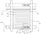
图1为现有技术提供的氧化物TFT阵列基板的俯视结构示意图;FIG. 1 is a schematic top view structure diagram of an oxide TFT array substrate provided by the prior art;
图2为现有技术提供的氧化物TFT阵列基板沿栅线上的A-A'向剖视结构示意图;2 is a schematic cross-sectional structure diagram of an oxide TFT array substrate provided by the prior art along the A-A' direction on the gate line;
图3为本发明实施例提供的氧化物TFT阵列基板的俯视结构示意图;3 is a schematic top view of an oxide TFT array substrate provided by an embodiment of the present invention;
图4为本发明实施例提供的氧化物TFT阵列基板沿栅线上的A-A'向剖视结构示意图;4 is a schematic cross-sectional structure diagram of an oxide TFT array substrate provided by an embodiment of the present invention along the A-A' direction on the gate line;
图5为本发明实施例提供的氧化物TFT阵列基板的制作方法的第一次构图工艺后的结构示意图;5 is a schematic structural diagram after the first patterning process of the method for manufacturing an oxide TFT array substrate provided by an embodiment of the present invention;
图6为本发明实施例提供的氧化物TFT阵列基板的制作方法的第二次构图工艺后的结构示意图;6 is a schematic structural view after the second patterning process of the method for manufacturing an oxide TFT array substrate provided by an embodiment of the present invention;
图7为本发明实施例提供的氧化物TFT阵列基板的制作方法的第三次构图工艺后的结构示意图;7 is a schematic structural diagram after the third patterning process of the method for manufacturing an oxide TFT array substrate provided by an embodiment of the present invention;
图8为本发明实施例提供的氧化物TFT阵列基板的制作方法的第四次构图工艺后的结构示意图。FIG. 8 is a schematic structural view after the fourth patterning process of the method for fabricating an oxide TFT array substrate according to an embodiment of the present invention.
图9为本发明实施例提供的氧化物TFT阵列基板的制作方法的第五次构图工艺后的结构示意图。FIG. 9 is a schematic structural diagram after the fifth patterning process of the method for fabricating an oxide TFT array substrate according to an embodiment of the present invention.
图10为本发明实施例提供的氧化物TFT阵列基板的制作方法的第六次构图工艺后的结构示意图。FIG. 10 is a schematic structural view after the sixth patterning process of the method for fabricating an oxide TFT array substrate according to an embodiment of the present invention.
图11(a)到图11(h)为本发明实施例提供的氧化物TFT阵列基板的制作流程示意图(半色调掩模技术)。FIG. 11( a ) to FIG. 11( h ) are schematic diagrams of the manufacturing process of the oxide TFT array substrate provided by the embodiment of the present invention (half-tone mask technology).
图12为本发明实施例提供的氧化物TFT阵列基板电路原理图。FIG. 12 is a schematic circuit diagram of an oxide TFT array substrate provided by an embodiment of the present invention.
附图标记说明:Explanation of reference signs:
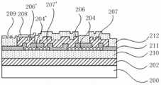
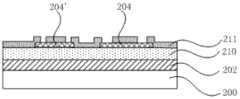
100:衬底基板;101:公共电极层;102:栅线/栅极;103:公共电极线;104:第一氧化物有源层;105:数据线;106:第一源极;107:第一漏极;108:像素电极上的狭缝;109:像素电极;110:栅绝缘层;111:刻蚀阻挡层;112:钝化层;200:衬底基板;201:公共电极层;202:栅线/栅极;203:公共电极线;204:第一氧化物有源层;204’:第二氧化物有源层;205:数据线;206:第一源极;206’:第二源极;207:第一漏极;207’:第二漏极;208:像素电极层;209:像素电极层上的狭缝;210:栅绝缘层;211:刻蚀阻挡层;212:钝化层。100: base substrate; 101: common electrode layer; 102: gate line/gate; 103: common electrode line; 104: first oxide active layer; 105: data line; 106: first source; 107: First drain; 108: slit on the pixel electrode; 109: pixel electrode; 110: gate insulating layer; 111: etching stopper layer; 112: passivation layer; 200: base substrate; 201: common electrode layer; 202: gate line/gate; 203: common electrode line; 204: first oxide active layer; 204': second oxide active layer; 205: data line; 206: first source; 206': 207: first drain; 207': second drain; 208: pixel electrode layer; 209: slit on the pixel electrode layer; 210: gate insulating layer; 211: etching barrier layer; 212 : passivation layer.
具体实施方式Detailed ways
下面结合附图和实施例,对本发明的具体实施方式作进一步详细描述。以下实施例用于说明本发明,但不能用来限制本发明的范围。The specific implementation manners of the present invention will be further described in detail below in conjunction with the accompanying drawings and embodiments. The following examples are used to illustrate the present invention, but should not be used to limit the scope of the present invention.
需要说明的是:本发明实施例的“上”“下”只是参考附图对本发明实施例进行说明,不作限定用语。在本发明实施例的描述中,术语“第一”、“第二”仅用于描述目的,而不能理解为指示或暗示相对重要性或者隐含指明所指示的技术特征的数量。It should be noted that "upper" and "lower" in the embodiments of the present invention are only used to describe the embodiments of the present invention with reference to the drawings, and are not used as limiting terms. In the description of the embodiments of the present invention, the terms "first" and "second" are used for description purposes only, and cannot be understood as indicating or implying relative importance or implicitly indicating the quantity of indicated technical features.
本实施例示例性地,以高级超维场转换(Advanced DimensionSwitch,ADS)型的氧化物TFT阵列基板的结构为例,具体描述该TFT阵列基板的结构。本实施例中所述第一氧化物TFT为原氧化物TFT,所述第一源极和第一漏极为原氧化物TFT的源极和漏极;第二氧化物TFT为本发明实施例所提供的虚拟氧化物TFT,所述第二源极和第二漏极为虚拟氧化物TFT的源极和漏极。In this embodiment, the structure of the TFT array substrate is specifically described by taking the structure of an advanced dimension switch (Advanced DimensionSwitch, ADS) type oxide TFT array substrate as an example. In this embodiment, the first oxide TFT is the original oxide TFT, and the first source and the first drain are the source and drain of the original oxide TFT; the second oxide TFT is the original oxide TFT in the embodiment of the present invention. In the dummy oxide TFT provided, the second source and the second drain are the source and drain of the dummy oxide TFT.
如图3、4所示,本发明提供了一种氧化物TFT阵列基板,包括:衬底基板200,设置于所述衬底基板200上的栅线202、数据线205以及多个像素单元,每个所述像素单元包括第一氧化物TFT、和像素电极208,其中,每个所述像素单元还包括至少一个与第一氧化物TFT串联的第二氧化物TFT,所述像素电极208与所述第二漏极207’相连,所述第二源极206’与所述第一漏极207相连,所述第一源极206与所述数据线205相连。As shown in Figures 3 and 4, the present invention provides an oxide TFT array substrate, including: a
上述氧化物TFT阵列基板,在现有技术提供只包括第一氧化物TFT的基础上,增加第二氧化物TFT。增加的第二氧化物TFT的作用在于:该第二氧化物TFT增加了像素电极208与数据线205之间关态电阻,能抑制第一氧化物有源层204内空穴流入第一漏极207,以及第一漏极207的电子流入第一氧化物有源层204中的几率,从而有效抑制“漏极→氧化物有源层→源极”的漏电路径,提升面板的显示品质,如图12所示,与第一氧化物TFT串联设置的第二氧化物TFT能够增大TFT的关态电阻(Roff1+Roff2>Roff1),达到减小漏电流的目的。The above-mentioned oxide TFT array substrate includes only the first oxide TFT on the basis of the prior art, and the second oxide TFT is added. The effect of the added second oxide TFT is: the second oxide TFT increases the off-state resistance between the
上述阵列基板具体包括:衬底基板200;设置在衬底基板200上的栅线202;设置在所述栅线202上方的栅绝缘层210;设置在所述栅绝缘层210上位于栅线202上方的第一氧化物有源层图案204和第二氧化物有源层图案204’;设置在所述第一氧化物有源层图案204和第二氧化物有源层图案204’上方的刻蚀阻挡层图案211;设置在所述刻蚀阻挡层图案211上方的所述第一源极图案206、第一漏极图案207、第二源极图案206’和第二漏极图案207’,所述第一源极图案206和第一漏极图案207通过刻蚀阻挡层图案211上的过孔与第一氧化物TFT的有源层图案204相连,所述第二源极图案206’和第二漏极图案207’通过刻蚀阻挡层图案211上的过孔与所述第二氧化物TFT的有源层图案204’相连;设置在所述源极和漏极上方的钝化层212,所述钝化层212设有过孔;其中,所述第二漏极207’与像素单元中延伸至所述第二漏极207’的像素电极层208相连。The above-mentioned array substrate specifically includes: a
需要说明的是,所述刻蚀阻挡层211设有过孔,以用于防止源极、漏极与氧化物有源层之间的接触,该刻蚀阻挡层211在制作氧化物TFT阵列基板过程中,用于防止形成源极和漏极的过程中源极和漏极之间形成的沟道内的氧化物有源层被刻蚀,刻蚀阻挡层211至少覆盖第一源极206和第一漏极207、第二源极206’和第二漏极207’之间的沟道,图4中示例性地示出除源极/漏极与氧化物有源层接触的区域外的栅极202的其它区域都覆盖刻蚀阻挡层211。在实际的制备过程中,刻蚀阻挡层211的图案可视实际制作工艺和要求而定,本发明对此不作具体限定。It should be noted that the
需要说明的是,上述基于图3、4所描述的TFT阵列基板的结构仅是以ADS型氧化物TFT阵列基板的底栅结构为例进行说明,但并不限制本发明仅适用于底栅结构的TFT阵列基板,同样适用于顶栅结构等TFT阵列基板。It should be noted that the structure of the TFT array substrate described above based on FIGS. 3 and 4 is only illustrated by taking the bottom gate structure of the ADS type oxide TFT array substrate as an example, but it does not limit the present invention to be applicable only to the bottom gate structure. TFT array substrates, also applicable to TFT array substrates such as top gate structure.
具体地,本领域所属技术人员很容易得出本发明所提供的底栅结构氧化物TFT阵列基板可以轻易改为顶栅结构氧化物TFT阵列基板,顶栅结构氧化物TFT阵列基板具体包括:衬底基板;设置在衬底基板上的第一氧化物有源层图案和第二氧化物有源层图案;设置在所述第一氧化物有源层图案和第二氧化物有源层图案上方的刻蚀阻挡层图案;设置在所述刻蚀阻挡层图案上方的所述第一源极图案、第一漏极图案、第二源极图案和第二漏极图案,所述第一源极图案和第一漏极图案通过刻蚀阻挡层图案上的过孔与第一氧化物TFT的有源层图案相连,所述第二源极图案和第二漏极图案通过刻蚀阻挡层图案上的过孔与所述第二氧化物TFT的有源层图案相连;设置在所述源极和漏极上方的栅绝缘层;设置在所述栅绝缘层上方的栅线;设置在所述上位于栅线上方的的钝化层,所述钝化层设有过孔;其中,所述第二漏极与像素单元中延伸至所述第二漏极的像素电极层相连。当然,本发明所提供的氧化物TFT阵列基板结构并不局限于本实施例中的所提供的氧化物TFT阵列基板结构,在此不再赘述。Specifically, those skilled in the art can easily find that the bottom gate structure oxide TFT array substrate provided by the present invention can be easily changed into a top gate structure oxide TFT array substrate, and the top gate structure oxide TFT array substrate specifically includes: Base substrate; a first oxide active layer pattern and a second oxide active layer pattern disposed on the base substrate; disposed above the first oxide active layer pattern and the second oxide active layer pattern The etch barrier pattern; the first source pattern, the first drain pattern, the second source pattern and the second drain pattern arranged above the etch barrier pattern, the first source The pattern and the first drain pattern are connected to the active layer pattern of the first oxide TFT through the via hole on the etching barrier layer pattern, and the second source pattern and the second drain pattern are connected through the etching barrier layer pattern. The via hole is connected to the active layer pattern of the second oxide TFT; the gate insulating layer arranged above the source and drain; the gate line arranged above the gate insulating layer; arranged on the A passivation layer located above the gate line, the passivation layer is provided with a via hole; wherein, the second drain is connected to the pixel electrode layer extending to the second drain in the pixel unit. Of course, the structure of the oxide TFT array substrate provided by the present invention is not limited to the structure of the oxide TFT array substrate provided in this embodiment, and details are not repeated here.
进一步地,所述阵列基板还包括:设置在衬底基板200上公共电极201和公共电极线203,所述公共电极线203与所述公共电极201相连。Further, the array substrate further includes: a
进一步地,所述公共电极201和所述像素电极208异层设置,处于相对上层的所述像素电极208或所述公共电极201具有狭缝状结构;处于相对下层的所述像素电极208或所述公共电极201具有板状结构;或所述公共电极201和所述像素电极208同层设置,所述像素电极208和所述公共电极201均具有狭缝状结构。Further, the
此外,需要说明的是,上述基于图3、4所描述的TFT阵列基板结构仅是以ADS型氧化物TFT阵列基板为例进行说明,但并不限制本发明仅适用于ADS型氧化物TFT阵列基板,同样适用于扭曲向列(Twisted Nematic,TN)型第一源极206、第一漏极207和第一氧化物TFT的有源层204直接接触的TFT阵列基板,在此本发明不作具体限定。In addition, it should be noted that the structure of the TFT array substrate described above based on FIGS. 3 and 4 is only illustrated by taking the ADS type oxide TFT array substrate as an example, but it does not limit the present invention to be applicable only to the ADS type oxide TFT array. The substrate is also applicable to the TFT array substrate in which the
进一步地,所述氧化物有源层为铟镓锌氧化物。Further, the oxide active layer is InGaZnO.
本发明实施例提供的一种氧化物TFT阵列基板,由于在现有技术提供只包括第一氧化物TFT的基础上,增加第二氧化物TFT,该第二氧化物TFT增加了像素电极与数据线之间的关态电阻,能够抑制“漏极→氧化物有源层→源极”的漏电路径,提升面板的显示品质;另一个角度,与第一氧化物TFT串联设置的第二氧化物TFT能够增大TFT的关态电阻(Roff1+Roff2>Roff1),达到减小漏电流的目的。An oxide TFT array substrate provided by an embodiment of the present invention adds a second oxide TFT on the basis of only the first oxide TFT provided in the prior art, and the second oxide TFT increases pixel electrodes and data The off-state resistance between the lines can suppress the leakage path of "drain → oxide active layer → source" and improve the display quality of the panel; another angle, the second oxide TFT arranged in series with the first oxide TFT The TFT can increase the off-state resistance of the TFT (Roff1 +Roff2 >Roff1 ), so as to reduce the leakage current.
基于上述氧化物TFT阵列基板,本发明实施例还提供了一种显示面板,该显示面板包括上述氧化物TFT阵列基板。Based on the above-mentioned oxide TFT array substrate, an embodiment of the present invention further provides a display panel, which includes the above-mentioned oxide TFT array substrate.
基于上述氧化物TFT阵列基板,本发明实施例还提供了一种氧化物TFT阵列基板的制备方法,该方法包括:通过构图工艺,在所述阵列基板上形成栅线202、数据线205、以及多个像素单元,每个所述像素单元包括第一氧化物薄膜晶体管和像素电极208,其中,每个所述像素单元还包括至少一个与所述第一氧化物薄膜晶体管串联的第二氧化物薄膜晶体管,所述像素电极208与所述第二漏极207’相连,所述第二源极206’与所述第一漏极207相连,所述第一源极206与所述数据线205相连。Based on the above-mentioned oxide TFT array substrate, an embodiment of the present invention also provides a method for preparing an oxide TFT array substrate, the method comprising: forming
具体的,本发明实施例以底栅型ADS型氧化物TFT阵列基板的制备方法为例进行详细描述,具体方法如下所述。需要说明的是,本发明实施例提供的构图工艺包括曝光、显影、刻蚀、灰化等主要工艺。Specifically, the embodiment of the present invention will be described in detail by taking a method for preparing a bottom-gate ADS oxide TFT array substrate as an example, and the specific method is as follows. It should be noted that the patterning process provided in the embodiment of the present invention includes main processes such as exposure, development, etching, and ashing.
S1、通过第一次构图工艺,在衬底基板200上形成包括公共电极201、栅线202和公共电极线203的图案。S1. Through the first patterning process, a pattern including
具体的,在第一次构图工艺过程中,首先在衬底基板200上栅金属层薄膜,然后在涂布有栅金属层的衬底基板200上形成光刻胶。如图11(a)到(h)所示,利用半色调掩模板对光刻胶进行曝光、显影后,形成光刻胶完全保留区域和光刻胶完全去除区域;其中,所述光刻胶保留区域对应公共电极201、栅线202和公共电极线203的区域;所述光刻胶去除区域对应所述像素单元中的除所述光刻胶完全保留区域以外的区域。利用刻蚀工艺去除掉光刻胶完全去除区域上的栅金属层薄膜,再利用灰化工艺剥离掉光刻胶完全保留区域的光刻胶,形成如图11(a)到(h)所示的公共电极201、栅线202和公共电极线203的图案。如图5所示,露出栅线202的图案,形成栅线202。Specifically, in the first patterning process, a thin film of the gate metal layer is first formed on the
S2、通过第二次构图工艺,在经过第一次构图工艺的衬底基板200上形成包括栅绝缘层210、第一氧化物有源层204和第二氧化物有源层204’的图案。其中,所述氧化物有源层的图案位于栅线202上方。S2. Through the second patterning process, a pattern including the
具体的,在第二次构图工艺的过程中,首先在经过第一次构图工艺的衬底基板200上涂布栅绝缘层薄膜和氧化物有源层薄膜。然后在涂布有栅绝缘层薄膜和氧化物有源层薄膜的衬底基板200上形成光刻胶。利用掩模板对光刻胶进行曝光、显影后,形成光刻胶完全保留区域和光刻胶完全去除区域;其中,所述光刻胶完全保留区域对应第一氧化物TFT的有源层204和第二氧化物TFT的有源层204’的区域;所述光刻胶完全去除区域对应所述像素单元中除所述光刻胶完全保留区域以外的区域。利用刻蚀工艺去除掉光刻胶完全去除区域上的氧化物有源层薄膜,再利用灰化工艺剥离掉光刻胶完全保留区域的光刻胶,如图6所示,露出第一氧化物TFT的有源层204和第二氧化物TFT的有源层204’的图案,形成栅绝缘层210和氧化物有源层。Specifically, in the process of the second patterning process, first, the gate insulating layer film and the oxide active layer film are coated on the
S3、通过第三次构图工艺,在经过第二次构图工艺的衬底基板200上形成包括刻蚀阻挡层211的图案。S3. Through the third patterning process, a pattern including the
具体的,在第三次构图工艺的过程中,首先在经过第二次构图工艺的衬底基板200上涂布刻蚀阻挡层薄膜,然后在涂布有刻蚀阻挡层薄膜的衬底基板200形成光刻胶。利用掩模板对光刻胶进行曝光、显影后,形成光刻胶完全保留区域和光刻胶完全去除区域;其中,所述光刻胶完全保留区域对应刻蚀阻挡层211的区域;所述光刻胶完全去除区域对应所述像素单元中除所述光刻胶完全保留区域以外的区域。利用刻蚀工艺去除掉光刻胶完全去除区域上的刻蚀阻挡层薄膜,再利用灰化工艺剥离掉光刻胶完全保留区域的光刻胶,如图7所示,露出刻蚀阻挡层211的图案,形成刻蚀阻挡层211。Specifically, in the process of the third patterning process, the etch barrier film is first coated on the
S4、通过第四次构图工艺,在经过第三次构图工艺的衬底基板200上形成包括数据线205、第一源极206、第一漏极207、第二源极206’和第二漏极207’的图案。S4. Through the fourth patterning process, on the
具体的,在第四次构图工艺的过程中,首先在经过第三次构图工艺的衬底基板200上涂布源漏金属层薄膜,然后在涂布有源漏金属层薄膜的衬底基板200形成光刻胶。利用掩模板对光刻胶进行曝光、显影后,形成光刻胶完全保留区域和光刻胶完全去除区域;其中,所述光刻胶完全保留区域对应数据线205、第一源极206、第一漏极207、第二源极206’和第二漏极207’的区域;所述光刻胶完全去除区域对应所述像素单元中除所述光刻胶完全保留区域以外的区域。利用刻蚀工艺去除掉光刻胶完全去除区域上的刻蚀阻挡层薄膜,再利用灰化工艺剥离掉光刻胶完全保留区域的光刻胶,形成如图3所示的数据线205、第一源极206、第一漏极207、第二源极206’和第二漏极207’的图案。如图8所示,露出源极、漏极的图案,形成源极、漏极。Specifically, in the process of the fourth patterning process, the source-drain metal layer thin film is first coated on the
S5、通过第五次构图工艺,在经过第四次构图工艺的衬底基板200上形成包括钝化层212的图案。S5. Through the fifth patterning process, a pattern including the
具体的,在第五次构图工艺的过程中,首先在经过第四次构图工艺的衬底基板200上涂布钝化层薄膜,然后在涂布有钝化层薄膜的衬底基板200形成光刻胶。利用掩模板对光刻胶进行曝光、显影后,形成光刻胶完全保留区域和光刻胶完全去除区域;其中,所述光刻胶完全保留区域对应钝化层212的区域;所述光刻胶完全去除区域对应所述像素单元中除所述光刻胶完全保留区域以外的区域,具体的所述光刻胶完全去除区域包括栅线引线过孔和数据线引线过孔。利用刻蚀工艺去除掉光刻胶完全去除区域上的钝化层薄膜,再利用灰化工艺剥离掉光刻胶完全保留区域的光刻胶,如图8所示,形成钝化层207的图案、栅线引线过孔和数据线引线过孔,其中栅线引线过孔和数据线引线过孔图中未示出。Specifically, in the process of the fifth patterning process, a passivation layer film is first coated on the
S6、通过第六次构图工艺,在经过第五次构图工艺的衬底基板200上形成包括像素电极208的图案,所述像素电极208延伸至所述第二漏极207’并与所述第二漏极207’相连。S6. Through the sixth patterning process, form a pattern including the
具体的,在第六次构图工艺的过程中,首先在经过第五次构图工艺的衬底基板200上涂布透明导电层薄膜,然后在涂布有透明导电层薄膜的衬底基板200形成光刻胶。利用掩模板对光刻胶进行曝光、显影后,形成光刻胶完全保留区域和光刻胶完全去除区域;其中,所述光刻胶完全保留区域对应像素电极208的区域;所述光刻胶完全去除区域对应所述像素单元中除所述光刻胶完全保留区域以外的区域。利用刻蚀工艺去除掉光刻胶完全去除区域上的透明导电层薄膜,再利用灰化工艺剥离掉光刻胶完全保留区域的光刻胶,如图9所示,形成具有狭缝209的像素电极208。Specifically, in the process of the sixth patterning process, a transparent conductive layer film is first coated on the
进一步地,本领域所属技术人员很容易得出本发明所提供的底栅结构氧化物TFT阵列基板可以轻易改为顶栅结构氧化物TFT阵列基板,与底栅结构氧化物TFT阵列基板结构制备方法步骤不同,顶栅结构氧化物TFT阵列基板制备方法具体包括:Further, those skilled in the art can easily conclude that the bottom gate structure oxide TFT array substrate provided by the present invention can be easily changed into a top gate structure oxide TFT array substrate, and the preparation method of the bottom gate structure oxide TFT array substrate structure The steps are different, and the preparation method of the oxide TFT array substrate with the top gate structure specifically includes:
S1’、通过第一次构图工艺,在衬底基板上形成包括第一氧化物有源层、第二氧化物有源层和公共电极的图案。S1'. Through the first patterning process, a pattern including the first oxide active layer, the second oxide active layer and the common electrode is formed on the base substrate.
具体的,在第一次构图工艺的过程中,首先在衬底基板上涂布透明导电薄膜、氧化物有源层薄膜。然后在涂布有透明导电薄膜、氧化物有源层薄膜的衬底基板上形成光刻胶。利用掩模板对光刻胶进行曝光、显影后,形成光刻胶完全保留区域和光刻胶完全去除区域;其中,所述光刻胶完全保留区域对应第一氧化物TFT的有源层和第二氧化物TFT的有源层的区域;所述光刻胶完全去除区域对应所述像素单元中除所述光刻胶完全保留区域以外的区域。利用刻蚀工艺去除掉光刻胶完全去除区域上的氧化物有源层薄膜,再利用灰化工艺剥离掉光刻胶完全保留区域的光刻胶,形成公共电极、第一氧化物TFT的有源层和第二氧化物TFT的有源层的图案。Specifically, in the process of the first patterning process, a transparent conductive film and an oxide active layer film are firstly coated on the base substrate. Then a photoresist is formed on the base substrate coated with a transparent conductive film and an oxide active layer film. After exposing and developing the photoresist by using a mask, a completely reserved region of photoresist and a completely removed region of photoresist are formed; wherein, the completely reserved region of photoresist corresponds to the active layer of the first oxide TFT and the second active layer of the oxide TFT. The area of the active layer of the dioxide TFT; the area where the photoresist is completely removed corresponds to the area of the pixel unit except the area where the photoresist is completely reserved. Use an etching process to remove the oxide active layer film on the area where the photoresist is completely removed, and then use an ashing process to strip off the photoresist in the area where the photoresist is completely reserved, to form the common electrode and the active layer of the first oxide TFT. source layer and the pattern of the active layer of the second oxide TFT.
S2’、通过第二次构图工艺,在经过第一次构图工艺的衬底基板上形成包括刻蚀阻挡层的图案。S2'. Through the second patterning process, a pattern including an etch barrier layer is formed on the base substrate that has undergone the first patterning process.
具体的,在第二次构图工艺的过程中,首先在经过第一次构图工艺的衬底基板上涂布刻蚀阻挡层薄膜,然后在涂布有刻蚀阻挡层薄膜的衬底基板形成光刻胶。利用掩模板对光刻胶进行曝光、显影后,形成光刻胶完全保留区域和光刻胶完全去除区域;其中,所述光刻胶完全保留区域对应刻蚀阻挡层的区域;所述光刻胶完全去除区域对应所述像素单元中除所述光刻胶完全保留区域以外的区域。利用刻蚀工艺去除掉光刻胶完全去除区域上的刻蚀阻挡层薄膜,再利用灰化工艺剥离掉光刻胶完全保留区域的光刻胶,形成刻蚀阻挡层的图案。Specifically, in the process of the second patterning process, firstly, the etch barrier film is coated on the base substrate that has undergone the first patterning process, and then the light is formed on the base substrate coated with the etch barrier film. Engraving. After exposing and developing the photoresist by using a mask, a completely reserved region of photoresist and a completely removed region of photoresist are formed; wherein, the region of completely reserved photoresist corresponds to the region of the etching barrier layer; the photoresist The completely removed area of glue corresponds to the area of the pixel unit except the area completely reserved for photoresist. The etch stop layer film on the photoresist completely removed area is removed by an etching process, and then the photoresist in the photoresist completely reserved area is stripped off by an ashing process to form a pattern of the etch stop layer.
S3’、通过第三次构图工艺,在经过第二次构图工艺的衬底基板上形成包括数据线、第一源极、第一漏极、第二源极和第二漏极的图案。S3'. Through the third patterning process, a pattern including the data line, the first source, the first drain, the second source and the second drain is formed on the base substrate after the second patterning process.
具体的,在第三次构图工艺的过程中,首先在经过第二次构图工艺的衬底基板上涂布源、漏金属层薄膜,然后在涂布有源、漏金属层薄膜的衬底基板形成光刻胶。利用掩模板对光刻胶进行曝光、显影后,形成光刻胶完全保留区域和光刻胶完全去除区域;其中,所述光刻胶完全保留区域对应数据线、第一源极、第一漏极、第二源极和第二漏极的区域;所述光刻胶完全去除区域对应所述像素单元中除所述光刻胶完全保留区域以外的区域。利用刻蚀工艺去除掉光刻胶完全去除区域上的刻蚀阻挡层薄膜,再利用灰化工艺剥离掉光刻胶完全保留区域的光刻胶,形成数据线、第一源极、第一漏极、第二源极和第二漏极的图案。Specifically, in the process of the third patterning process, the source and drain metal layer thin films are first coated on the base substrate after the second patterning process, and then the source and drain metal layer thin films are coated on the base substrate Form photoresist. After exposing and developing the photoresist by using a mask, a completely reserved region of photoresist and a completely removed region of photoresist are formed; wherein, the completely reserved region of photoresist corresponds to the data line, the first source electrode, and the first drain The region of the electrode, the second source electrode and the second drain electrode; the region where the photoresist is completely removed corresponds to the region of the pixel unit except the region where the photoresist is completely reserved. Use an etching process to remove the etch barrier layer film on the area where the photoresist is completely removed, and then use an ashing process to strip off the photoresist in the area where the photoresist is completely reserved to form the data line, the first source electrode, and the first drain. pole, second source and second drain patterns.
S4’、通过第四次构图工艺,在经过第三次构图工艺的衬底基板上形成包括栅绝缘层、栅线、和公共电极线的图案。S4'. Through the fourth patterning process, a pattern including a gate insulating layer, a gate line, and a common electrode line is formed on the base substrate that has undergone the third patterning process.
具体的,在第四次构图工艺的过程中,首先在经过第三次构图工艺的衬底基板上涂布栅绝缘层薄膜和栅金属层薄膜。然后在涂布有栅绝缘层薄膜和栅金属层薄膜的衬底基板上形成光刻胶。利用掩模板对光刻胶进行曝光、显影后,形成光刻胶完全保留区域和光刻胶完全去除区域;其中,所述光刻胶完全保留区域对应栅金属层薄膜的区域;所述光刻胶完全去除区域对应所述像素单元中除所述光刻胶完全保留区域以外的区域。利用刻蚀工艺去除掉光刻胶完全去除区域上的栅金属层薄膜,再利用灰化工艺剥离掉光刻胶完全保留区域的光刻胶,形成栅绝缘层、栅线和公共电极线的图案。Specifically, in the process of the fourth patterning process, first, the gate insulating layer film and the gate metal layer film are coated on the substrate after the third patterning process. Then a photoresist is formed on the base substrate coated with the gate insulating layer thin film and the gate metal layer thin film. After exposing and developing the photoresist by using a mask, a completely reserved region of photoresist and a completely removed region of photoresist are formed; wherein, the completely reserved region of photoresist corresponds to the region of the gate metal layer film; the photoresist The completely removed area of glue corresponds to the area of the pixel unit except the area completely reserved for photoresist. Use an etching process to remove the gate metal layer film on the area where the photoresist is completely removed, and then use an ashing process to strip off the photoresist in the area where the photoresist is completely reserved to form the pattern of the gate insulating layer, gate lines and common electrode lines .
S5’、通过第五次构图工艺,在经过第四次构图工艺的衬底基板上形成包括钝化层的图案。S5'. Through the fifth patterning process, a pattern including a passivation layer is formed on the base substrate that has undergone the fourth patterning process.
具体的,在第五次构图工艺的过程中,首先在经过第四次构图工艺的衬底基板上涂布钝化层薄膜,然后在涂布有钝化层薄膜的衬底基板形成光刻胶。利用掩模板对光刻胶进行曝光、显影后,形成光刻胶完全保留区域和光刻胶完全去除区域;其中,所述光刻胶完全保留区域对应钝化层的区域;所述光刻胶完全去除区域对应所述像素单元中除所述光刻胶完全保留区域以外的区域,具体的所述光刻胶完全去除区域包括栅线引线过孔和数据线引线过孔。利用刻蚀工艺去除掉光刻胶完全去除区域上的钝化层薄膜,再利用灰化工艺剥离掉光刻胶完全保留区域的光刻胶,形成钝化层的图案、栅线引线过孔和数据线引线过孔。Specifically, in the process of the fifth patterning process, a passivation layer film is first coated on the base substrate of the fourth patterning process, and then a photoresist is formed on the base substrate coated with the passivation layer film . After using the mask to expose and develop the photoresist, a completely reserved region of photoresist and a completely removed region of photoresist are formed; wherein, the region of completely retained photoresist corresponds to the region of the passivation layer; the photoresist The completely removed area corresponds to the area of the pixel unit except for the completely reserved area of the photoresist, and specifically the completely removed area of the photoresist includes gate line lead via holes and data line lead via holes. Use an etching process to remove the passivation layer film on the area where the photoresist is completely removed, and then use an ashing process to strip off the photoresist in the area where the photoresist is completely reserved to form the pattern of the passivation layer, the gate wire lead via hole and Data cable lead through hole.
S6’、通过第六次构图工艺,在经过第五次构图工艺的衬底基板上形成包括像素电极的图案。S6'. Through the sixth patterning process, a pattern including the pixel electrode is formed on the base substrate after the fifth patterning process.
具体的,在第六次构图工艺的过程中,首先在经过第五次构图工艺的衬底基板上涂布透明导电层薄膜,然后在涂布有透明导电层薄膜的衬底基板形成光刻胶。利用掩模板对光刻胶进行曝光、显影后,形成光刻胶完全保留区域和光刻胶完全去除区域;其中,所述光刻胶完全保留区域对应像素电极的区域;所述光刻胶完全去除区域对应所述像素单元中除所述光刻胶完全保留区域以外的区域。利用刻蚀工艺去除掉光刻胶完全去除区域上的透明导电层薄膜,再利用灰化工艺剥离掉光刻胶完全保留区域的光刻胶,形成具有狭缝的像素电极。Specifically, in the process of the sixth patterning process, a transparent conductive layer film is first coated on the base substrate of the fifth patterning process, and then a photoresist is formed on the base substrate coated with the transparent conductive layer film. . After the photoresist is exposed and developed by using the mask plate, a photoresist completely reserved area and a photoresist completely removed area are formed; wherein, the photoresist completely reserved area corresponds to the area of the pixel electrode; the photoresist is completely The removed area corresponds to the area of the pixel unit except for the completely reserved area of the photoresist. Using an etching process to remove the transparent conductive layer film on the area where the photoresist is completely removed, and then using an ashing process to strip off the photoresist in the area where the photoresist is completely reserved, to form a pixel electrode with a slit.
需要说明的是,本发明实施例描述的氧化物TFT阵列基板的制备方法仅示例性的六次构图工艺进行描述,但不能理解为限制本发明仅能采用六次构图工艺实现。其它不同构图工艺次数,能够在所述阵列基板还包括第二氧化物TFT的制备方法,也属于本发明的保护范围。本发明实施例提供的一种氧化物TFT阵列基板的制作方法,在阵列基板上设置有第二氧化物TFT,由于在现有技术提供只包括第一氧化物TFT的基础上,增加第二氧化物TFT,该第二氧化物TFT增加了像素电极与数据线之间的关态电阻,能够抑制“漏极→氧化物有源层→源极”的漏电路径,提升面板的显示品质;另一个角度,与第一氧化物TFT串联设置的第二氧化物TFT能够增大TFT的关态电阻(Roff1+Roff2>Roff1),达到减小漏电流的目的。此外,当氧化物TFT开启时,信号由第一氧化物TFT的有源层传至第一漏极,接着传至第二源极,经第二氧化物TFT的有源层传至第二漏极,再通过像素电极上的钝化层过孔传送至像素电极,最终可在液晶盒内形成横向电场,供液晶偏转,通过控制数据信号,可控制液晶偏转角度,影响面板透过率。It should be noted that the manufacturing method of the oxide TFT array substrate described in the embodiment of the present invention is only described as an exemplary six-patterning process, but it should not be understood as limiting the present invention to be realized only by using six patterning processes. Other different patterning process times, which can also include the second oxide TFT preparation method on the array substrate, also belong to the protection scope of the present invention. An embodiment of the present invention provides a method for manufacturing an oxide TFT array substrate. A second oxide TFT is provided on the array substrate. Since the prior art only includes the first oxide TFT, the second oxide TFT is added. The second oxide TFT increases the off-state resistance between the pixel electrode and the data line, which can suppress the leakage path of "drain → oxide active layer → source" and improve the display quality of the panel; the other Angle, the second oxide TFT arranged in series with the first oxide TFT can increase the off-state resistance of the TFT (Roff1 +Roff2 >Roff1 ), so as to reduce the leakage current. In addition, when the oxide TFT is turned on, the signal is transmitted from the active layer of the first oxide TFT to the first drain, then to the second source, and then to the second drain through the active layer of the second oxide TFT. electrode, and then transmitted to the pixel electrode through the passivation layer on the pixel electrode, and finally a transverse electric field can be formed in the liquid crystal cell for deflection of the liquid crystal. By controlling the data signal, the deflection angle of the liquid crystal can be controlled to affect the transmittance of the panel.
以上实施方式仅用于说明本发明,而并非对本发明的限制,有关技术领域的普通技术人员,在不脱离本发明的精神和范围的情况下,还可以做出各种变化和变型,因此所有等同的技术方案也属于本发明的范畴,本发明的专利保护范围应由权利要求限定。The above embodiments are only used to illustrate the present invention, but not to limit the present invention. Those of ordinary skill in the relevant technical field can make various changes and modifications without departing from the spirit and scope of the present invention. Therefore, all Equivalent technical solutions also belong to the category of the present invention, and the scope of patent protection of the present invention should be defined by the claims.
Claims (11)
Translated fromChinesePriority Applications (3)
| Application Number | Priority Date | Filing Date | Title |
|---|---|---|---|
| CN201410057337.6ACN103811503A (en) | 2014-02-19 | 2014-02-19 | Array substrate and preparation method and display panel |
| US14/435,913US9947691B2 (en) | 2014-02-19 | 2014-08-15 | Array substrate, manufacturing method thereof and display panel |
| PCT/CN2014/084530WO2015123975A1 (en) | 2014-02-19 | 2014-08-15 | Array substrate and preparation method therefor, and display panel |
Applications Claiming Priority (1)
| Application Number | Priority Date | Filing Date | Title |
|---|---|---|---|
| CN201410057337.6ACN103811503A (en) | 2014-02-19 | 2014-02-19 | Array substrate and preparation method and display panel |
Publications (1)
| Publication Number | Publication Date |
|---|---|
| CN103811503Atrue CN103811503A (en) | 2014-05-21 |
Family
ID=50708037
Family Applications (1)
| Application Number | Title | Priority Date | Filing Date |
|---|---|---|---|
| CN201410057337.6APendingCN103811503A (en) | 2014-02-19 | 2014-02-19 | Array substrate and preparation method and display panel |
Country Status (3)
| Country | Link |
|---|---|
| US (1) | US9947691B2 (en) |
| CN (1) | CN103811503A (en) |
| WO (1) | WO2015123975A1 (en) |
Cited By (8)
| Publication number | Priority date | Publication date | Assignee | Title |
|---|---|---|---|---|
| WO2015123975A1 (en)* | 2014-02-19 | 2015-08-27 | 京东方科技集团股份有限公司 | Array substrate and preparation method therefor, and display panel |
| CN104966696A (en)* | 2015-05-06 | 2015-10-07 | 深圳市华星光电技术有限公司 | Manufacturing method of thin film transistor (TFT) substrate and TFT substrate structure |
| WO2016033981A1 (en)* | 2014-09-01 | 2016-03-10 | 京东方科技集团股份有限公司 | Thin film transistor and manufacturing method therefor, array substrate and display device |
| CN107577365A (en)* | 2017-08-24 | 2018-01-12 | 京东方科技集团股份有限公司 | A kind of touch display substrate, device and driving method |
| CN108337905A (en)* | 2016-11-17 | 2018-07-27 | 华为技术有限公司 | A kind of array substrate and preparation method thereof, liquid crystal display panel |
| US10256343B2 (en) | 2015-09-30 | 2019-04-09 | Boe Technology Group Co., Ltd. | Thin film transistor, array substrate and their manufacturing methods, and display apparatus |
| CN115497381A (en)* | 2022-09-23 | 2022-12-20 | 深圳莱宝高科技股份有限公司 | Array substrate, display panel and display |
| WO2025076647A1 (en)* | 2023-10-08 | 2025-04-17 | 京东方科技集团股份有限公司 | Display panel and display device comprising same |
Families Citing this family (6)
| Publication number | Priority date | Publication date | Assignee | Title |
|---|---|---|---|---|
| US20200212227A1 (en)* | 2016-08-17 | 2020-07-02 | Boe Technology Group Co., Ltd. | Thin film transistor, manufacturing method thereof, array substrate, display device |
| US10212009B2 (en)* | 2017-03-06 | 2019-02-19 | Blackberry Limited | Modulation for a data bit stream |
| CN113192981B (en)* | 2018-03-21 | 2023-07-25 | 福建华佳彩有限公司 | A kind of preparation method of TFT substrate, display device and TFT substrate |
| US10665622B2 (en)* | 2018-07-17 | 2020-05-26 | Shenzhen China Star Optoelectronics Semiconductor Display Technology Co., Ltd. | Manufacturing method of array substrate and array substrate |
| CN109564916B (en)* | 2018-10-12 | 2022-06-28 | 京东方科技集团股份有限公司 | Substrate for electronic device, display device, method of manufacturing substrate for electronic device |
| JP2021039291A (en)* | 2019-09-05 | 2021-03-11 | 株式会社ジャパンディスプレイ | Semiconductor device |
Citations (5)
| Publication number | Priority date | Publication date | Assignee | Title |
|---|---|---|---|---|
| US5410164A (en)* | 1989-01-18 | 1995-04-25 | Sharp Kabushimi Kaisha | Display electrode substrate |
| US20030112383A1 (en)* | 2001-12-14 | 2003-06-19 | Dong-Gyu Kim | Liquid crystal display, thin film transistor array panel for liquid crystal display and method of manufacturing the same |
| CN1550859A (en)* | 1995-02-15 | 2004-12-01 | ��ʽ����뵼����Դ�о��� | Liquid crystal display device having a plurality of pixel electrodes |
| CN102473736A (en)* | 2009-09-01 | 2012-05-23 | 夏普株式会社 | Semiconductor device, active matrix substrate, and display device |
| CN203707132U (en)* | 2014-02-19 | 2014-07-09 | 合肥鑫晟光电科技有限公司 | Array substrate and display panel |
Family Cites Families (18)
| Publication number | Priority date | Publication date | Assignee | Title |
|---|---|---|---|---|
| JP3485667B2 (en)* | 1995-01-28 | 2004-01-13 | 株式会社半導体エネルギー研究所 | Active matrix display device |
| JP3527034B2 (en)* | 1996-09-20 | 2004-05-17 | 株式会社半導体エネルギー研究所 | Semiconductor device |
| US6420758B1 (en)* | 1998-11-17 | 2002-07-16 | Semiconductor Energy Laboratory Co., Ltd. | Semiconductor device having an impurity region overlapping a gate electrode |
| TW517260B (en)* | 1999-05-15 | 2003-01-11 | Semiconductor Energy Lab | Semiconductor device and method for its fabrication |
| TW543206B (en)* | 1999-06-28 | 2003-07-21 | Semiconductor Energy Lab | EL display device and electronic device |
| JP4831885B2 (en)* | 2001-04-27 | 2011-12-07 | 株式会社半導体エネルギー研究所 | Method for manufacturing semiconductor device |
| JP2003051556A (en)* | 2001-08-03 | 2003-02-21 | Sanyo Electric Co Ltd | Semiconductor storage device |
| CN1822385B (en)* | 2005-01-31 | 2013-02-06 | 株式会社半导体能源研究所 | Display device and electronic equipment containing same |
| KR100688971B1 (en)* | 2006-02-16 | 2007-03-08 | 삼성전자주식회사 | Display device |
| KR100747491B1 (en)* | 2006-02-20 | 2007-08-08 | 삼성전자주식회사 | Display device |
| KR20070122317A (en)* | 2006-06-26 | 2007-12-31 | 삼성전자주식회사 | Liquid crystal module, driving method and liquid crystal display device |
| KR101261609B1 (en) | 2006-07-06 | 2013-05-06 | 삼성디스플레이 주식회사 | Thin film transistor, thin film transistor array panel and method for manufacturing the same |
| US8723260B1 (en)* | 2009-03-12 | 2014-05-13 | Rf Micro Devices, Inc. | Semiconductor radio frequency switch with body contact |
| CN102484136A (en)* | 2009-08-28 | 2012-05-30 | 夏普株式会社 | Semiconductor device, active matrix substrate, and display device |
| KR101339001B1 (en) | 2012-07-04 | 2013-12-09 | 엘지디스플레이 주식회사 | Array substrate for liquid crystal display device and method for fabricating the same |
| CN103187423B (en) | 2013-02-04 | 2016-03-23 | 合肥京东方光电科技有限公司 | A kind of oxide film transistor array substrate and preparation method thereof, display floater |
| KR102100927B1 (en)* | 2013-08-05 | 2020-05-15 | 삼성전자주식회사 | High electron mobility transistor, method of manufacturing the same and electronic device including transistor |
| CN103811503A (en)* | 2014-02-19 | 2014-05-21 | 合肥鑫晟光电科技有限公司 | Array substrate and preparation method and display panel |
- 2014
- 2014-02-19CNCN201410057337.6Apatent/CN103811503A/enactivePending
- 2014-08-15USUS14/435,913patent/US9947691B2/enactiveActive
- 2014-08-15WOPCT/CN2014/084530patent/WO2015123975A1/enactiveApplication Filing
Patent Citations (5)
| Publication number | Priority date | Publication date | Assignee | Title |
|---|---|---|---|---|
| US5410164A (en)* | 1989-01-18 | 1995-04-25 | Sharp Kabushimi Kaisha | Display electrode substrate |
| CN1550859A (en)* | 1995-02-15 | 2004-12-01 | ��ʽ����뵼����Դ�о��� | Liquid crystal display device having a plurality of pixel electrodes |
| US20030112383A1 (en)* | 2001-12-14 | 2003-06-19 | Dong-Gyu Kim | Liquid crystal display, thin film transistor array panel for liquid crystal display and method of manufacturing the same |
| CN102473736A (en)* | 2009-09-01 | 2012-05-23 | 夏普株式会社 | Semiconductor device, active matrix substrate, and display device |
| CN203707132U (en)* | 2014-02-19 | 2014-07-09 | 合肥鑫晟光电科技有限公司 | Array substrate and display panel |
Cited By (14)
| Publication number | Priority date | Publication date | Assignee | Title |
|---|---|---|---|---|
| US9947691B2 (en) | 2014-02-19 | 2018-04-17 | Boe Technology Group Co., Ltd. | Array substrate, manufacturing method thereof and display panel |
| WO2015123975A1 (en)* | 2014-02-19 | 2015-08-27 | 京东方科技集团股份有限公司 | Array substrate and preparation method therefor, and display panel |
| WO2016033981A1 (en)* | 2014-09-01 | 2016-03-10 | 京东方科技集团股份有限公司 | Thin film transistor and manufacturing method therefor, array substrate and display device |
| US9634033B2 (en) | 2014-09-01 | 2017-04-25 | Boe Technology Group Co., Ltd. | Thin film transistor and method of manufacturing the same, array substrate and display apparatus |
| CN104966696A (en)* | 2015-05-06 | 2015-10-07 | 深圳市华星光电技术有限公司 | Manufacturing method of thin film transistor (TFT) substrate and TFT substrate structure |
| WO2016176884A1 (en)* | 2015-05-06 | 2016-11-10 | 深圳市华星光电技术有限公司 | Manufacturing method for tft substrate and structure thereof |
| CN104966696B (en)* | 2015-05-06 | 2017-11-28 | 深圳市华星光电技术有限公司 | The preparation method and its structure of TFT substrate |
| US10256343B2 (en) | 2015-09-30 | 2019-04-09 | Boe Technology Group Co., Ltd. | Thin film transistor, array substrate and their manufacturing methods, and display apparatus |
| CN108337905A (en)* | 2016-11-17 | 2018-07-27 | 华为技术有限公司 | A kind of array substrate and preparation method thereof, liquid crystal display panel |
| CN107577365A (en)* | 2017-08-24 | 2018-01-12 | 京东方科技集团股份有限公司 | A kind of touch display substrate, device and driving method |
| US10691239B2 (en) | 2017-08-24 | 2020-06-23 | Boe Technology Group Co., Ltd. | Touch display substrate, driving method thereof, and touch display device |
| CN107577365B (en)* | 2017-08-24 | 2021-01-26 | 京东方科技集团股份有限公司 | Touch display substrate, device and driving method |
| CN115497381A (en)* | 2022-09-23 | 2022-12-20 | 深圳莱宝高科技股份有限公司 | Array substrate, display panel and display |
| WO2025076647A1 (en)* | 2023-10-08 | 2025-04-17 | 京东方科技集团股份有限公司 | Display panel and display device comprising same |
Also Published As
| Publication number | Publication date |
|---|---|
| US20160027801A1 (en) | 2016-01-28 |
| US9947691B2 (en) | 2018-04-17 |
| WO2015123975A1 (en) | 2015-08-27 |
Similar Documents
| Publication | Publication Date | Title |
|---|---|---|
| CN103811503A (en) | Array substrate and preparation method and display panel | |
| CN103499906B (en) | Array substrate, manufacturing method of array substrate and display device | |
| CN103187423B (en) | A kind of oxide film transistor array substrate and preparation method thereof, display floater | |
| CN104867870B (en) | Manufacturing method and structure of double gate oxide semiconductor TFT substrate | |
| CN105470262A (en) | Thin film transistor substrate and display apparatus using the same | |
| CN102983135B (en) | The preparation method of a kind of array base palte, display unit and array base palte | |
| CN105097675A (en) | Array substrate and preparation method thereof | |
| CN105470197A (en) | Production method of low temperature poly silicon array substrate | |
| US20180292696A1 (en) | Array substrate, manufacturing method thereof, display panel and display device | |
| CN108666218A (en) | Thin film transistor, display substrate, manufacturing method thereof, and display device | |
| CN104752343A (en) | Manufacturing method and structure of substrate of bigrid oxide semiconductor TFT (thin film transistor) | |
| CN102629608B (en) | Array substrate, a manufacturing method thereof and display device | |
| CN105226015A (en) | A kind of tft array substrate and preparation method thereof | |
| WO2017156885A1 (en) | Thin film transistor, array substrate and manufacturing and driving method thereof, and display device | |
| CN105702687A (en) | TFT (Thin Film Transistor) substrate and manufacturing method thereof | |
| CN103915451A (en) | Array substrate, manufacturing method thereof and display device | |
| US10134765B2 (en) | Oxide semiconductor TFT array substrate and method for manufacturing the same | |
| CN104916649A (en) | Array substrate and manufacturing method thereof | |
| CN104157609B (en) | The preparation method and its structure of TFT substrate | |
| CN106935660A (en) | Thin film transistor (TFT) and preparation method thereof, array base palte and display device | |
| CN210403734U (en) | Display substrate and display device | |
| CN104576526B (en) | A kind of array substrate and preparation method thereof and display device | |
| CN105702586A (en) | Thin film transistor, array substrate, production method of thin film transistor and display device | |
| CN102709235B (en) | Array base board as well as manufacturing method and display device thereof | |
| WO2021097995A1 (en) | Array substrate and preparation method therefor |
Legal Events
| Date | Code | Title | Description |
|---|---|---|---|
| C06 | Publication | ||
| PB01 | Publication | ||
| C10 | Entry into substantive examination | ||
| SE01 | Entry into force of request for substantive examination | ||
| RJ01 | Rejection of invention patent application after publication | ||
| RJ01 | Rejection of invention patent application after publication | Application publication date:20140521 |