CN103811148A - Winding inductor for switching power supply and switching power supply with winding inductor - Google Patents
Winding inductor for switching power supply and switching power supply with winding inductorDownload PDFInfo
- Publication number
- CN103811148A CN103811148ACN201210449298.5ACN201210449298ACN103811148ACN 103811148 ACN103811148 ACN 103811148ACN 201210449298 ACN201210449298 ACN 201210449298ACN 103811148 ACN103811148 ACN 103811148A
- Authority
- CN
- China
- Prior art keywords
- buffer pad
- magnetic core
- wire
- power supply
- switching power
- Prior art date
- Legal status (The legal status is an assumption and is not a legal conclusion. Google has not performed a legal analysis and makes no representation as to the accuracy of the status listed.)
- Pending
Links
Images
Classifications
- H—ELECTRICITY
- H01—ELECTRIC ELEMENTS
- H01F—MAGNETS; INDUCTANCES; TRANSFORMERS; SELECTION OF MATERIALS FOR THEIR MAGNETIC PROPERTIES
- H01F27/00—Details of transformers or inductances, in general
- H01F27/33—Arrangements for noise damping
- H—ELECTRICITY
- H01—ELECTRIC ELEMENTS
- H01F—MAGNETS; INDUCTANCES; TRANSFORMERS; SELECTION OF MATERIALS FOR THEIR MAGNETIC PROPERTIES
- H01F5/00—Coils
- H01F5/02—Coils wound on non-magnetic supports, e.g. formers
Landscapes
- Engineering & Computer Science (AREA)
- Power Engineering (AREA)
- Coils Or Transformers For Communication (AREA)
Abstract
Translated fromChineseDescription
Translated fromChinese技术领域technical field
本发明涉及开关电源,具体涉及一种用于开关电源的绕线电感和具有该绕线电感的开关电源。The invention relates to a switching power supply, in particular to a winding inductance for a switching power supply and a switching power supply with the winding inductance.
背景技术Background technique
开关电源凭借其小型化、重量轻、输入电压范围广、热消耗较少等众多优点,已经逐渐取代线性电源而被应用于各种电子产品。开关电源包含的主要部件包括绕线电感。在开关电源的绕线电感的线圈中的电流通常会大于20A,并且众所周知的开关电源的瞬态负载变化较快,这样就会导致磁性体(即绕线电感的磁芯)产生明显的磁致伸缩现象。磁致伸缩是指磁性体由于磁化状态的改变,其尺寸在各方向发生变化。Switching power supplies have gradually replaced linear power supplies and are used in various electronic products due to their many advantages such as miniaturization, light weight, wide input voltage range, and less heat consumption. The main components contained in switching power supplies include wound inductors. The current in the coil of the winding inductor of the switching power supply is usually greater than 20A, and the transient load of the well-known switching power supply changes quickly, which will cause the magnetic body (that is, the core of the winding inductor) to produce obvious magnetic induction. Telescopic phenomenon. Magnetostriction means that the size of a magnetic body changes in all directions due to the change of the magnetization state.
磁致伸缩会导致磁性体内发生自然的震动现象,进而导致绕线电感的磁芯与线圈之间发生碰撞,这种震动和碰撞会使开关电源产生令人厌烦的噪声。如前所述,震动是属于磁致伸缩现象导致的磁性体内发生的不可避免的自然现象,这是无法避免的。并且通常情况下,碰撞所产生的噪声的分贝值要大于震动所产生的噪声的分贝值,因此可以通过降低碰撞所产生的噪声来有效地降低开关电源工作时的分贝值。Magnetostriction causes a natural vibration phenomenon in the magnetic body, which in turn causes the core of the wire wound inductor to collide with the coil. This vibration and collision can cause annoying noise in the switching power supply. As mentioned earlier, vibration is an inevitable natural phenomenon that occurs in a magnetic body caused by magnetostriction, which cannot be avoided. And usually, the decibel value of the noise generated by the collision is greater than the decibel value of the noise generated by the vibration, so the decibel value of the switching power supply can be effectively reduced by reducing the noise generated by the collision.
因此,需要一种用于开关电源的绕线电感和具有该绕线电感的开关电源,以解决现有技术中存在的问题。Therefore, there is a need for a wire-wound inductance for a switching power supply and a switching power supply with the wire-wound inductance to solve the problems in the prior art.
发明内容Contents of the invention
为了解决上述问题,根据本发明的一个方面,提供了一种用于开关电源的绕线电感,所述绕线电感包括磁芯和卷绕在所述磁芯上的线圈,在所述磁芯和所述线圈之间设置有缓冲垫,所述缓冲垫是由弹性材料形成的,且所述缓冲垫的厚度大于所述磁芯和所述线圈之间的径向间隙。In order to solve the above problems, according to one aspect of the present invention, a wound inductor for a switching power supply is provided, the wound inductor includes a magnetic core and a coil wound on the magnetic core, in the magnetic core A buffer pad is arranged between the coil and the coil, the buffer pad is formed of elastic material, and the thickness of the buffer pad is greater than the radial gap between the magnetic core and the coil.
优选地,所述缓冲垫是由耐高温的弹性材料形成的。Preferably, the buffer pad is formed of high temperature resistant elastic material.
优选地,所述缓冲垫覆盖在所述磁芯上与所述线圈相对应的区域。Preferably, the buffer pad covers a region on the magnetic core corresponding to the coil.
优选地,所述缓冲垫呈管状。Preferably, the buffer pad is in the shape of a tube.
优选地,所述缓冲垫上设置有沿着所述绕线电感的轴向延伸的轴向切口。Preferably, the buffer pad is provided with an axial cut extending along the axial direction of the winding inductor.
优选地,所述轴向切口的宽度小于或等于所述缓冲垫的周长的3/4。Preferably, the width of the axial slit is less than or equal to 3/4 of the circumference of the buffer pad.
优选地,所述缓冲垫上设置有沿着所述绕线电感的周向延伸的周向切口。Preferably, the buffer pad is provided with a circumferential cut extending along the circumferential direction of the winding inductor.
优选地,所述缓冲垫上设置有多个周向切口,所述多个周向切口均匀地分布。Preferably, the buffer pad is provided with a plurality of circumferential cuts, and the plurality of circumferential cuts are evenly distributed.
优选地,所述缓冲垫上设置有多个散热孔。Preferably, the buffer pad is provided with a plurality of cooling holes.
优选地,所述缓冲垫是由磁的不良导体形成的。Preferably, the cushion is formed from a poor conductor of magnetism.
根据本发明的另一个方面,还提供了一种开关电源,所述开关电源包括绕线电感,所述绕线电感包括磁芯和卷绕在所述磁芯上的线圈,在所述磁芯和所述线圈之间设置有缓冲垫,所述缓冲垫是由弹性材料形成的,且所述缓冲垫的厚度大于所述磁芯和所述线圈之间的径向间隙。According to another aspect of the present invention, a switching power supply is also provided. The switching power supply includes a wire-wound inductor, and the wire-wound inductor includes a magnetic core and a coil wound on the magnetic core. In the magnetic core A buffer pad is arranged between the coil and the coil, the buffer pad is formed of elastic material, and the thickness of the buffer pad is greater than the radial gap between the magnetic core and the coil.
优选地,所述缓冲垫是由耐高温的弹性材料形成的。Preferably, the buffer pad is formed of high temperature resistant elastic material.
优选地,所述缓冲垫覆盖在所述磁芯上与所述线圈相对应的区域。Preferably, the buffer pad covers a region on the magnetic core corresponding to the coil.
优选地,所述缓冲垫呈管状。Preferably, the buffer pad is in the shape of a tube.
优选地,所述缓冲垫上设置有沿着所述绕线电感的轴向延伸的轴向切口。Preferably, the buffer pad is provided with an axial cut extending along the axial direction of the winding inductor.
优选地,所述轴向切口的宽度小于或等于所述缓冲垫的周长的3/4。Preferably, the width of the axial slit is less than or equal to 3/4 of the circumference of the buffer pad.
优选地,所述缓冲垫上设置有沿着所述绕线电感的周向延伸的周向切口。Preferably, the buffer pad is provided with a circumferential cut extending along the circumferential direction of the winding inductor.
优选地,所述缓冲垫上设置有多个周向切口,所述多个周向切口均匀地分布。Preferably, the buffer pad is provided with a plurality of circumferential cuts, and the plurality of circumferential cuts are evenly distributed.
优选地,所述缓冲垫上设置有多个散热孔。Preferably, the buffer pad is provided with a plurality of cooling holes.
优选地,所述缓冲垫是由磁的不良导体形成的。Preferably, the cushion is formed from a poor conductor of magnetism.
本发明提供的绕线电感在磁芯和线圈之间设置缓冲垫可以吸收由于磁致伸缩现象而导致的磁芯的尺寸改变,保持部件的相对位置固定,并且还可以避免在磁芯与线圈之间产生碰撞,进而降低噪声。In the wire-wound inductor provided by the present invention, a buffer pad is provided between the magnetic core and the coil to absorb the size change of the magnetic core caused by magnetostriction, keep the relative position of the components fixed, and also avoid the gap between the magnetic core and the coil. Collisions occur between them, thereby reducing noise.
在发明内容部分中引入了一系列简化形式的概念,这将在具体实施方式部分中进一步详细说明。本发明内容部分并不意味着要试图限定出所要求保护的技术方案的关键特征和必要技术特征,更不意味着试图确定所要求保护的技术方案的保护范围。A series of concepts in simplified form are introduced in the Summary of the Invention, which will be further detailed in the Detailed Description. The summary of the present invention does not mean trying to limit the key features and essential technical features of the claimed technical solution, nor does it mean trying to determine the protection scope of the claimed technical solution.
以下结合附图,详细说明本发明的优点和特征。The advantages and features of the present invention will be described in detail below in conjunction with the accompanying drawings.
附图说明Description of drawings
本发明的下列附图在此作为本发明的一部分用于理解本发明。附图中示出了本发明的实施例及其描述,用来解释本发明的原理。在附图中,The following drawings of the invention are hereby included as part of the invention for understanding the invention. The accompanying drawings illustrate embodiments of the invention and description thereof to explain principles of the invention. In the attached picture,
图1为根据本发明一个实施例的绕线电感的示意图;Fig. 1 is the schematic diagram of the wirewound inductor according to an embodiment of the present invention;
图2为根据本发明一个实施例的缓冲垫的示意图;以及Figure 2 is a schematic diagram of a cushioning pad according to one embodiment of the present invention; and
图3为根据本发明另一个实施例的缓冲垫的示意图。Fig. 3 is a schematic diagram of a cushioning pad according to another embodiment of the present invention.
具体实施方式Detailed ways
在下文的描述中,给出了大量具体的细节以便提供对本发明更为彻底的理解。然而,对于本领域技术人员来说显而易见的是,本发明可以无需一个或多个这些细节而得以实施。在其他的例子中,为了避免与本发明发生混淆,对于本领域公知的一些技术特征未进行描述。In the following description, numerous specific details are given in order to provide a more thorough understanding of the present invention. It will be apparent, however, to one skilled in the art that the present invention may be practiced without one or more of these details. In other examples, some technical features known in the art are not described in order to avoid confusion with the present invention.
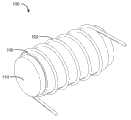
根据本发明的一个方面,提供一种用于开关电源的绕线电感(以下简称“绕线电感”)。图1为根据本发明一个实施例的绕线电感的示意图,下面将结合图1对该绕线电感进行详细描述。According to one aspect of the present invention, a wire-wound inductor (hereinafter referred to as "wire-wound inductor") for a switching power supply is provided. FIG. 1 is a schematic diagram of a wire-wound inductor according to an embodiment of the present invention. The wire-wound inductor will be described in detail below with reference to FIG. 1 .
如图1所示,绕线电感100包括磁芯110和线圈120。磁芯110是由导磁材料形成的,所述导磁材料包括但不限于纯铁、低碳钢、铁硅合金、铁铝合金、铁硅铝合金、镍铁合金、铁钴合金和/或软磁材料中的一种或多种。线圈120卷绕在磁芯110上,线圈120可以包括具有较高导电率的金属线(例如,银线、铜线和铝线等)和包裹在金属线表面的绝缘层。As shown in FIG. 1 , the
为了适应线圈120通电后磁芯110所产生的磁致伸缩现象,在磁芯110和线圈120之间可以形成一定的径向间隙,即,使线圈120的外径略大于磁芯110的内径。在磁芯110和线圈120之间的径向间隙内可以设置缓冲垫130。缓冲垫130可以由诸如橡胶的弹性材料形成,并且缓冲垫130的厚度大于磁芯110和线圈120之间的径向间隙。在自然状态下,缓冲垫130受到磁芯110和线圈120的挤压而产生一定的弹性形变。这样,即使由于线圈120内的瞬态负载变化导致磁芯110的尺寸缩小也不会在磁芯110和缓冲垫130之间以及缓冲垫130和线圈120之间产生间隙,因而不会由于碰撞而产生噪声。相反地,如果导致磁芯110因线圈120内的瞬态负载变化而增大尺寸,由于缓冲垫130是由弹性材料形成的,因此也不会对磁芯110的尺寸增大产生影响。In order to adapt to the magnetostriction produced by the
一方面,线圈120通常会有较大电流强度的电流通过,线圈120本身会产生热量;另一方面,磁芯110内的磁场强度和磁场方向在不断地改变导致磁芯110内分子运动剧烈,磁芯110也会产生热量,因此,优选地,缓冲垫130可以由耐高温的弹性材料形成。根据使用该绕线电感100的开关电源的应用,主要考虑线圈120内的电流强度及其改变,本领域的技术人员可以对缓冲垫130的材料进行合理选择。On the one hand, the
为了节约材料,降低成本,在线圈120未完全覆盖磁芯110的情况下,优选地,缓冲垫130可以仅覆盖在磁芯110上与线圈120相对应的区域。In order to save materials and reduce costs, if the
在制造绕线电感100的过程中,通常是先将缓冲垫130覆盖在磁芯110上,然后将导线卷绕在包覆有缓冲垫130的磁芯110上。为了便于缓冲垫130固定在磁芯110上,并有利于实现各个部件的标准化生产,优选地,缓冲垫130可以呈管状。In the process of manufacturing the
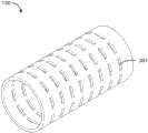
根据本发明一个实施例,缓冲垫130上可以设置有沿着绕线电感的轴向延伸的轴向切口201,如图2所示。轴向切口201贯穿缓冲垫130的轴向长度,该轴向切口201不但可以增大缓冲垫130沿着其径向方向上的弹性,而且还可以方便地将缓冲垫130安装在磁芯110上。优选地,缓冲垫130上仅设置一个轴向切口201,以保证缓冲垫130为整块的、单体构件。轴向切口201的宽度可以根据缓冲垫130的尺寸进行调节,但考虑到要尽量避免磁芯110与线圈120接触,优选地,轴向切口201的宽度可以小于或等于缓冲垫130的周长的3/4,以使缓冲垫130覆盖磁芯110的四分之三的圆周。According to an embodiment of the present invention, the
根据本发明另一个实施例,缓冲垫130上可以设置有沿着绕线电感的周向延伸的周向切口301,如图3所示。周向切口301在管状的缓冲垫130的周向上间断地设置,以使缓冲垫130为整块的、单体构件。周向切口301不限于图3中所示出的矩形,其还可以具有其他形状。多个周向切口301可以如图3所示地以矩阵方式排列,也可以交错地排列。此外,周向切口301还可以贯通缓冲垫130的整个圆周,即周向切口301可以将缓冲垫130分割成多个相对独立的部分。需要说明的是,缓冲垫130上可以设置有一个周向切口301,也可以设置为多个周向切口301。周向切口301不会对缓冲垫130在磁芯110上的固定产生影响。在缓冲垫130上设置周向切口301可以增大缓冲垫130沿着其轴向方向上的弹性。周向切口301也可以增大缓冲垫130在径向方向上的弹性。当然,周向切口301所引起的缓冲垫130在周向和径向方向上的弹性与周向切口301的形状和排列方式有关,本领域的技术人员可以根据需要来合理地设置周向切口301。为了使缓冲垫130的弹性分布均匀,优选地,多个周向切口301均匀地分布在缓冲垫130上。According to another embodiment of the present invention, the
前面已经提到,磁芯110和线圈120本身都能够产生热量,因此,优选地,可以在缓冲垫130上设置多个散热孔202,如图2中所示。散热孔202可以使磁芯110产生的热量扩散到环境中,而且还能够在磁芯110的热量和线圈120的热量之间形成对流,进而有利于热量的传递。需要说明的是,当缓冲垫130上设置有多个周向切口301时,该周向切口301也可以起到散热的功能。散热孔202和周向切口301在功能上具有一定的重叠,但不意味着两者不可以在同一个缓冲垫130上同时存在。As mentioned above, both the
另外,为了避免缓冲垫130对磁芯110中的磁场产生影响,优选地,缓冲垫130是由磁的不良导体形成的。In addition, in order to avoid the impact of the
根据本发明的另一个方面,还提供一种开关电源,该开关电源包括如上所述的任意一种绕线电感。关于绕线电感中包含的各个部件的形状和结构可以参见上文相应部分的描述,这里不再详述。According to another aspect of the present invention, a switching power supply is also provided, and the switching power supply includes any one of the above-mentioned winding inductors. For the shapes and structures of the various components included in the wire wound inductor, reference may be made to the descriptions in the corresponding parts above, and details will not be described here.
综上所述,本发明提供的绕线电感在磁芯和线圈之间设置缓冲垫可以吸收由于磁致伸缩现象而导致的磁芯的尺寸改变,保持部件的相对位置固定,并且还可以避免在磁芯与线圈之间产生碰撞,进而降低噪声。To sum up, in the wire wound inductor provided by the present invention, the buffer pad between the magnetic core and the coil can absorb the size change of the magnetic core caused by the magnetostrictive phenomenon, keep the relative position of the components fixed, and also avoid the Collision between the core and the coil reduces noise.
本发明已经通过上述实施例进行了说明,但应当理解的是,一个实施例的结构和功能可以在另一个实施例中采用。在特定实施例中所有优点并非必须同时存在。从现有技术看是独特的每个特征,无论单独的或与其它特征相结合,也应当被认为是申请人的进一步发明的单独描述,包括由这样的特征所体现的结构性构思和/或功能性构思。上述实施例只是用于举例和说明的目的,而非意在将本发明限制于所描述的实施例范围内。此外本领域技术人员可以理解的是,本发明并不局限于上述实施例,根据本发明的教导还可以做出更多种的变型和修改,这些变型和修改均落在本发明所要求保护的范围以内。本发明的保护范围由附属的权利要求书及其等效范围所界定。The present invention has been described through the above embodiments, but it should be understood that the structures and functions of one embodiment can be adopted in another embodiment. Not all advantages need to be present in a particular embodiment at the same time. Each feature which is unique from the prior art, alone or in combination with other features, should also be considered as a separate description of a further invention of the applicant, including the structural idea and/or Functional idea. The above-described embodiments are for purposes of illustration and description only, and are not intended to limit the invention to the described embodiments. In addition, those skilled in the art can understand that the present invention is not limited to the above-mentioned embodiments, and more variations and modifications can be made according to the teachings of the present invention, and these variations and modifications all fall within the claimed scope of the present invention. within the range. The protection scope of the present invention is defined by the appended claims and their equivalent scope.
Claims (20)
Translated fromChinesePriority Applications (4)
| Application Number | Priority Date | Filing Date | Title |
|---|---|---|---|
| CN201210449298.5ACN103811148A (en) | 2012-11-09 | 2012-11-09 | Winding inductor for switching power supply and switching power supply with winding inductor |
| US13/910,989US20140132384A1 (en) | 2012-11-09 | 2013-06-05 | Wirewound inductor of switching power supply and switching power supply with the wirewound inductor |
| TW102138278ATW201428779A (en) | 2012-11-09 | 2013-10-23 | Wire wound inductor of switching power supply and switching power supply with the wirewound inductor |
| DE102013221664.5ADE102013221664A1 (en) | 2012-11-09 | 2013-10-24 | Wire-wound inductor of a switched-mode power supply and switched-mode power supply with the wire-wound inductor |
Applications Claiming Priority (1)
| Application Number | Priority Date | Filing Date | Title |
|---|---|---|---|
| CN201210449298.5ACN103811148A (en) | 2012-11-09 | 2012-11-09 | Winding inductor for switching power supply and switching power supply with winding inductor |
Publications (1)
| Publication Number | Publication Date |
|---|---|
| CN103811148Atrue CN103811148A (en) | 2014-05-21 |
Family
ID=50556035
Family Applications (1)
| Application Number | Title | Priority Date | Filing Date |
|---|---|---|---|
| CN201210449298.5APendingCN103811148A (en) | 2012-11-09 | 2012-11-09 | Winding inductor for switching power supply and switching power supply with winding inductor |
Country Status (4)
| Country | Link |
|---|---|
| US (1) | US20140132384A1 (en) |
| CN (1) | CN103811148A (en) |
| DE (1) | DE102013221664A1 (en) |
| TW (1) | TW201428779A (en) |
Cited By (1)
| Publication number | Priority date | Publication date | Assignee | Title |
|---|---|---|---|---|
| CN110911094A (en)* | 2019-12-05 | 2020-03-24 | 龙南县方成科技有限公司 | Surround durable inductor |
Families Citing this family (2)
| Publication number | Priority date | Publication date | Assignee | Title |
|---|---|---|---|---|
| KR101533081B1 (en)* | 2014-09-26 | 2015-07-03 | 성균관대학교산학협력단 | Redundancy-ready control apparatus, redundancy system and method for configuring redundant logics for assuring low power consumption and reliability at the same time |
| US11562854B1 (en)* | 2019-07-12 | 2023-01-24 | Bel Power Solutions Inc. | Dual slotted bobbin magnetic component with two-legged core |
Citations (8)
| Publication number | Priority date | Publication date | Assignee | Title |
|---|---|---|---|---|
| CH316009A (en)* | 1952-02-22 | 1956-09-15 | Siemens Ag | Coil with a cast resin coil body consisting of a tubular body and flanges, in particular for transducers or the like |
| DE2118084A1 (en)* | 1971-04-14 | 1972-10-26 | Licentia Patent-Verwaltungs-Gmbh, 6000 Frankfurt | Broadband transmitters in communications engineering |
| JPS5445735A (en)* | 1977-09-19 | 1979-04-11 | Hitachi Ltd | Mold transformer |
| US5951881A (en)* | 1996-07-22 | 1999-09-14 | President And Fellows Of Harvard College | Fabrication of small-scale cylindrical articles |
| US6690255B2 (en)* | 2002-02-21 | 2004-02-10 | Coilcraft, Incorporated | Electronic component |
| CN1871673A (en)* | 2003-10-23 | 2006-11-29 | 株式会社东芝 | Inductive device and method for manufacturing same |
| US20090313812A1 (en)* | 2008-06-24 | 2009-12-24 | Sergey Pulnikov | Method for making electrical windings for electrical apparatus and transformers and winding obtained by said method |
| WO2011010471A1 (en)* | 2009-07-24 | 2011-01-27 | 株式会社 東芝 | Coil antenna and electronic device using same |
- 2012
- 2012-11-09CNCN201210449298.5Apatent/CN103811148A/enactivePending
- 2013
- 2013-06-05USUS13/910,989patent/US20140132384A1/ennot_activeAbandoned
- 2013-10-23TWTW102138278Apatent/TW201428779A/enunknown
- 2013-10-24DEDE102013221664.5Apatent/DE102013221664A1/ennot_activeWithdrawn
Patent Citations (8)
| Publication number | Priority date | Publication date | Assignee | Title |
|---|---|---|---|---|
| CH316009A (en)* | 1952-02-22 | 1956-09-15 | Siemens Ag | Coil with a cast resin coil body consisting of a tubular body and flanges, in particular for transducers or the like |
| DE2118084A1 (en)* | 1971-04-14 | 1972-10-26 | Licentia Patent-Verwaltungs-Gmbh, 6000 Frankfurt | Broadband transmitters in communications engineering |
| JPS5445735A (en)* | 1977-09-19 | 1979-04-11 | Hitachi Ltd | Mold transformer |
| US5951881A (en)* | 1996-07-22 | 1999-09-14 | President And Fellows Of Harvard College | Fabrication of small-scale cylindrical articles |
| US6690255B2 (en)* | 2002-02-21 | 2004-02-10 | Coilcraft, Incorporated | Electronic component |
| CN1871673A (en)* | 2003-10-23 | 2006-11-29 | 株式会社东芝 | Inductive device and method for manufacturing same |
| US20090313812A1 (en)* | 2008-06-24 | 2009-12-24 | Sergey Pulnikov | Method for making electrical windings for electrical apparatus and transformers and winding obtained by said method |
| WO2011010471A1 (en)* | 2009-07-24 | 2011-01-27 | 株式会社 東芝 | Coil antenna and electronic device using same |
Cited By (2)
| Publication number | Priority date | Publication date | Assignee | Title |
|---|---|---|---|---|
| CN110911094A (en)* | 2019-12-05 | 2020-03-24 | 龙南县方成科技有限公司 | Surround durable inductor |
| CN110911094B (en)* | 2019-12-05 | 2021-11-26 | 龙南县方成科技有限公司 | Surround durable inductor |
Also Published As
| Publication number | Publication date |
|---|---|
| US20140132384A1 (en) | 2014-05-15 |
| TW201428779A (en) | 2014-07-16 |
| DE102013221664A1 (en) | 2014-05-15 |
Similar Documents
| Publication | Publication Date | Title |
|---|---|---|
| US9019062B2 (en) | Inductive device with improved core properties | |
| US20190148049A1 (en) | Inductor and mounting structure thereof | |
| US20100148902A1 (en) | Surface mount type power inductor | |
| JP5824001B2 (en) | Trance | |
| TW201301315A (en) | Magnetic element | |
| TW201346949A (en) | Magnetic element having heat-dissipating bobbin base | |
| JP2019079838A (en) | Transformer device | |
| CN103811148A (en) | Winding inductor for switching power supply and switching power supply with winding inductor | |
| JP5189637B2 (en) | Coil parts and power supply circuit using the same | |
| JP2007243131A (en) | Reactor part | |
| JP6171384B2 (en) | Trance | |
| CN109215942B (en) | Inductance element and LC filter | |
| JP5713232B2 (en) | Noise filter | |
| JP2018190910A (en) | Reactor device and manufacturing method thereof | |
| JP2009105164A (en) | Transformer | |
| CN105895335B (en) | Coil assembly, high current inductor comprising same and high current reactor comprising same | |
| JP6064943B2 (en) | Electronics | |
| JP2012204814A (en) | Core, transformer, choke coil and switching power supply device | |
| JP2016105464A (en) | Magnetic component and electric power transmitter | |
| JP2019504488A (en) | Inductance circuit with passive thermal management | |
| JP2012235051A (en) | Coil component | |
| JP3187497U (en) | Magnetic parts | |
| CN205159066U (en) | A flat wire square vertical winding inductor and inductor | |
| JP6160071B2 (en) | Inductor | |
| JP2002164235A (en) | Leakage transformer, power supply unit, and lighting fixture |
Legal Events
| Date | Code | Title | Description |
|---|---|---|---|
| C06 | Publication | ||
| PB01 | Publication | ||
| C10 | Entry into substantive examination | ||
| SE01 | Entry into force of request for substantive examination | ||
| C02 | Deemed withdrawal of patent application after publication (patent law 2001) | ||
| WD01 | Invention patent application deemed withdrawn after publication | Application publication date:20140521 |