CN103794502A - Semiconductor device and method for manufacturing the same - Google Patents
Semiconductor device and method for manufacturing the sameDownload PDFInfo
- Publication number
- CN103794502A CN103794502ACN201210424681.5ACN201210424681ACN103794502ACN 103794502 ACN103794502 ACN 103794502ACN 201210424681 ACN201210424681 ACN 201210424681ACN 103794502 ACN103794502 ACN 103794502A
- Authority
- CN
- China
- Prior art keywords
- layer
- gate
- substrate
- semi
- device manufacturing
- Prior art date
- Legal status (The legal status is an assumption and is not a legal conclusion. Google has not performed a legal analysis and makes no representation as to the accuracy of the status listed.)
- Pending
Links
- 238000000034methodMethods0.000titleclaimsabstractdescription52
- 239000004065semiconductorSubstances0.000titleclaimsabstractdescription26
- 238000004519manufacturing processMethods0.000titleclaimsabstractdescription22
- 239000000758substrateSubstances0.000claimsabstractdescription38
- 229910052751metalInorganic materials0.000claimsabstractdescription34
- 239000002184metalSubstances0.000claimsabstractdescription33
- 229910052721tungstenInorganic materials0.000claimsabstractdescription11
- WFKWXMTUELFFGS-UHFFFAOYSA-NtungstenChemical compound[W]WFKWXMTUELFFGS-UHFFFAOYSA-N0.000claimsabstractdescription10
- 239000010937tungstenSubstances0.000claimsabstractdescription10
- 239000010410layerSubstances0.000claimsdescription113
- 239000000463materialSubstances0.000claimsdescription26
- ATJFFYVFTNAWJD-UHFFFAOYSA-NTinChemical group[Sn]ATJFFYVFTNAWJD-UHFFFAOYSA-N0.000claimsdescription10
- 229910052581Si3N4Inorganic materials0.000claimsdescription7
- 230000008021depositionEffects0.000claimsdescription7
- HQVNEWCFYHHQES-UHFFFAOYSA-Nsilicon nitrideChemical compoundN12[Si]34N5[Si]62N3[Si]51N64HQVNEWCFYHHQES-UHFFFAOYSA-N0.000claimsdescription7
- 239000012212insulatorSubstances0.000claimsdescription5
- 238000000137annealingMethods0.000claimsdescription4
- CBENFWSGALASAD-UHFFFAOYSA-NOzoneChemical compound[O-][O+]=OCBENFWSGALASAD-UHFFFAOYSA-N0.000claimsdescription3
- 229910010038TiAlInorganic materials0.000claimsdescription3
- 239000008367deionised waterSubstances0.000claimsdescription3
- 229910021641deionized waterInorganic materials0.000claimsdescription3
- 239000011229interlayerSubstances0.000claimsdescription3
- 238000007254oxidation reactionMethods0.000claimsdescription3
- 239000000126substanceSubstances0.000claimsdescription3
- XLYOFNOQVPJJNP-UHFFFAOYSA-NwaterChemical compoundOXLYOFNOQVPJJNP-UHFFFAOYSA-N0.000claimsdescription3
- 230000015572biosynthetic processEffects0.000claimsdescription2
- 230000000903blocking effectEffects0.000abstractdescription5
- 238000000231atomic layer depositionMethods0.000description25
- 125000006850spacer groupChemical group0.000description15
- VYPSYNLAJGMNEJ-UHFFFAOYSA-NSilicium dioxideChemical compoundO=[Si]=OVYPSYNLAJGMNEJ-UHFFFAOYSA-N0.000description9
- 238000000151depositionMethods0.000description9
- 229910052710siliconInorganic materials0.000description8
- XUIMIQQOPSSXEZ-UHFFFAOYSA-NSiliconChemical compound[Si]XUIMIQQOPSSXEZ-UHFFFAOYSA-N0.000description7
- 230000004888barrier functionEffects0.000description7
- 238000005240physical vapour depositionMethods0.000description7
- 239000010703siliconSubstances0.000description7
- 238000005530etchingMethods0.000description6
- 229910052814silicon oxideInorganic materials0.000description5
- 238000007796conventional methodMethods0.000description4
- 238000000623plasma-assisted chemical vapour depositionMethods0.000description4
- 238000001039wet etchingMethods0.000description4
- 229910003481amorphous carbonInorganic materials0.000description3
- 238000004518low pressure chemical vapour depositionMethods0.000description3
- 150000002739metalsChemical class0.000description3
- 238000001451molecular beam epitaxyMethods0.000description3
- 150000004767nitridesChemical class0.000description3
- 229910021420polycrystalline siliconInorganic materials0.000description3
- -1Si 3 N 4 or SiNxChemical class0.000description2
- 229910004298SiO 2Inorganic materials0.000description2
- 229910052782aluminiumInorganic materials0.000description2
- 229910021417amorphous siliconInorganic materials0.000description2
- 238000006243chemical reactionMethods0.000description2
- 238000010586diagramMethods0.000description2
- 238000001312dry etchingMethods0.000description2
- 230000000694effectsEffects0.000description2
- 238000005516engineering processMethods0.000description2
- 229910052731fluorineInorganic materials0.000description2
- 229910052732germaniumInorganic materials0.000description2
- 238000005468ion implantationMethods0.000description2
- 229910021424microcrystalline siliconInorganic materials0.000description2
- 238000012986modificationMethods0.000description2
- 230000004048modificationEffects0.000description2
- 229910052750molybdenumInorganic materials0.000description2
- 229920000620organic polymerPolymers0.000description2
- 230000003647oxidationEffects0.000description2
- 229920005591polysiliconPolymers0.000description2
- 239000002243precursorSubstances0.000description2
- 229910021332silicideInorganic materials0.000description2
- FVBUAEGBCNSCDD-UHFFFAOYSA-Nsilicide(4-)Chemical compound[Si-4]FVBUAEGBCNSCDD-UHFFFAOYSA-N0.000description2
- 239000000377silicon dioxideSubstances0.000description2
- WGTYBPLFGIVFAS-UHFFFAOYSA-Mtetramethylammonium hydroxideChemical compound[OH-].C[N+](C)(C)CWGTYBPLFGIVFAS-UHFFFAOYSA-M0.000description2
- 229910018072Al 2 O 3Inorganic materials0.000description1
- 229910052582BNInorganic materials0.000description1
- PZNSFCLAULLKQX-UHFFFAOYSA-NBoron nitrideChemical compoundN#BPZNSFCLAULLKQX-UHFFFAOYSA-N0.000description1
- OKTJSMMVPCPJKN-UHFFFAOYSA-NCarbonChemical compound[C]OKTJSMMVPCPJKN-UHFFFAOYSA-N0.000description1
- YCKRFDGAMUMZLT-UHFFFAOYSA-NFluorine atomChemical compound[F]YCKRFDGAMUMZLT-UHFFFAOYSA-N0.000description1
- 229910002601GaNInorganic materials0.000description1
- 229910001218Gallium arsenideInorganic materials0.000description1
- 229910000673Indium arsenideInorganic materials0.000description1
- 229910021193La 2 O 3Inorganic materials0.000description1
- 229910020684PbZrInorganic materials0.000description1
- 229910004205SiNXInorganic materials0.000description1
- BLRPTPMANUNPDV-UHFFFAOYSA-NSilaneChemical compound[SiH4]BLRPTPMANUNPDV-UHFFFAOYSA-N0.000description1
- 229910000577Silicon-germaniumInorganic materials0.000description1
- 125000003118aryl groupChemical group0.000description1
- 239000005380borophosphosilicate glassSubstances0.000description1
- 229910052799carbonInorganic materials0.000description1
- 239000003610charcoalSubstances0.000description1
- 238000005229chemical vapour depositionMethods0.000description1
- 150000001875compoundsChemical class0.000description1
- 229910052802copperInorganic materials0.000description1
- 230000007547defectEffects0.000description1
- 229910003460diamondInorganic materials0.000description1
- 239000010432diamondSubstances0.000description1
- ZOCHARZZJNPSEU-UHFFFAOYSA-NdiboronChemical compoundB#BZOCHARZZJNPSEU-UHFFFAOYSA-N0.000description1
- 238000010891electric arcMethods0.000description1
- 238000001704evaporationMethods0.000description1
- 230000008020evaporationEffects0.000description1
- 230000005669field effectEffects0.000description1
- 238000011049fillingMethods0.000description1
- 239000011737fluorineSubstances0.000description1
- 229940104869fluorosilicateDrugs0.000description1
- GNPVGFCGXDBREM-UHFFFAOYSA-Ngermanium atomChemical compound[Ge]GNPVGFCGXDBREM-UHFFFAOYSA-N0.000description1
- 239000011521glassSubstances0.000description1
- WPYVAWXEWQSOGY-UHFFFAOYSA-Nindium antimonideChemical compound[Sb]#[In]WPYVAWXEWQSOGY-UHFFFAOYSA-N0.000description1
- RPQDHPTXJYYUPQ-UHFFFAOYSA-Nindium arsenideChemical compound[In]#[As]RPQDHPTXJYYUPQ-UHFFFAOYSA-N0.000description1
- 229910052747lanthanoidInorganic materials0.000description1
- 150000002602lanthanoidsChemical class0.000description1
- 238000001755magnetron sputter depositionMethods0.000description1
- 229910044991metal oxideInorganic materials0.000description1
- 150000004706metal oxidesChemical class0.000description1
- 229910052759nickelInorganic materials0.000description1
- JMANVNJQNLATNU-UHFFFAOYSA-NoxalonitrileChemical compoundN#CC#NJMANVNJQNLATNU-UHFFFAOYSA-N0.000description1
- 229910052698phosphorusInorganic materials0.000description1
- 229910052697platinumInorganic materials0.000description1
- 125000003367polycyclic groupChemical group0.000description1
- 239000011148porous materialSubstances0.000description1
- 238000007650screen-printingMethods0.000description1
- 229910000077silaneInorganic materials0.000description1
- LIVNPJMFVYWSIS-UHFFFAOYSA-Nsilicon monoxideChemical compound[Si-]#[O+]LIVNPJMFVYWSIS-UHFFFAOYSA-N0.000description1
- 239000002210silicon-based materialSubstances0.000description1
- 238000002791soakingMethods0.000description1
- 238000004528spin coatingMethods0.000description1
- 238000005507sprayingMethods0.000description1
- 238000004544sputter depositionMethods0.000description1
- 229910052717sulfurInorganic materials0.000description1
- 229910052715tantalumInorganic materials0.000description1
- NXHILIPIEUBEPD-UHFFFAOYSA-Htungsten hexafluorideChemical compoundF[W](F)(F)(F)(F)FNXHILIPIEUBEPD-UHFFFAOYSA-H0.000description1
Images


Classifications
- H—ELECTRICITY
- H10—SEMICONDUCTOR DEVICES; ELECTRIC SOLID-STATE DEVICES NOT OTHERWISE PROVIDED FOR
- H10D—INORGANIC ELECTRIC SEMICONDUCTOR DEVICES
- H10D64/00—Electrodes of devices having potential barriers
- H10D64/01—Manufacture or treatment
- H10D64/017—Manufacture or treatment using dummy gates in processes wherein at least parts of the final gates are self-aligned to the dummy gates, i.e. replacement gate processes
- H—ELECTRICITY
- H01—ELECTRIC ELEMENTS
- H01L—SEMICONDUCTOR DEVICES NOT COVERED BY CLASS H10
- H01L21/00—Processes or apparatus adapted for the manufacture or treatment of semiconductor or solid state devices or of parts thereof
- H01L21/02—Manufacture or treatment of semiconductor devices or of parts thereof
- H01L21/04—Manufacture or treatment of semiconductor devices or of parts thereof the devices having potential barriers, e.g. a PN junction, depletion layer or carrier concentration layer
- H01L21/18—Manufacture or treatment of semiconductor devices or of parts thereof the devices having potential barriers, e.g. a PN junction, depletion layer or carrier concentration layer the devices having semiconductor bodies comprising elements of Group IV of the Periodic Table or AIIIBV compounds with or without impurities, e.g. doping materials
- H01L21/28—Manufacture of electrodes on semiconductor bodies using processes or apparatus not provided for in groups H01L21/20 - H01L21/268
- H01L21/28008—Making conductor-insulator-semiconductor electrodes
- H01L21/28017—Making conductor-insulator-semiconductor electrodes the insulator being formed after the semiconductor body, the semiconductor being silicon
- H01L21/28026—Making conductor-insulator-semiconductor electrodes the insulator being formed after the semiconductor body, the semiconductor being silicon characterised by the conductor
- H01L21/28079—Making conductor-insulator-semiconductor electrodes the insulator being formed after the semiconductor body, the semiconductor being silicon characterised by the conductor the final conductor layer next to the insulator being a single metal, e.g. Ta, W, Mo, Al
- H—ELECTRICITY
- H01—ELECTRIC ELEMENTS
- H01L—SEMICONDUCTOR DEVICES NOT COVERED BY CLASS H10
- H01L21/00—Processes or apparatus adapted for the manufacture or treatment of semiconductor or solid state devices or of parts thereof
- H01L21/02—Manufacture or treatment of semiconductor devices or of parts thereof
- H01L21/04—Manufacture or treatment of semiconductor devices or of parts thereof the devices having potential barriers, e.g. a PN junction, depletion layer or carrier concentration layer
- H01L21/18—Manufacture or treatment of semiconductor devices or of parts thereof the devices having potential barriers, e.g. a PN junction, depletion layer or carrier concentration layer the devices having semiconductor bodies comprising elements of Group IV of the Periodic Table or AIIIBV compounds with or without impurities, e.g. doping materials
- H01L21/28—Manufacture of electrodes on semiconductor bodies using processes or apparatus not provided for in groups H01L21/20 - H01L21/268
- H01L21/28008—Making conductor-insulator-semiconductor electrodes
- H01L21/28017—Making conductor-insulator-semiconductor electrodes the insulator being formed after the semiconductor body, the semiconductor being silicon
- H01L21/28026—Making conductor-insulator-semiconductor electrodes the insulator being formed after the semiconductor body, the semiconductor being silicon characterised by the conductor
- H01L21/28088—Making conductor-insulator-semiconductor electrodes the insulator being formed after the semiconductor body, the semiconductor being silicon characterised by the conductor the final conductor layer next to the insulator being a composite, e.g. TiN
- H—ELECTRICITY
- H01—ELECTRIC ELEMENTS
- H01L—SEMICONDUCTOR DEVICES NOT COVERED BY CLASS H10
- H01L21/00—Processes or apparatus adapted for the manufacture or treatment of semiconductor or solid state devices or of parts thereof
- H01L21/02—Manufacture or treatment of semiconductor devices or of parts thereof
- H01L21/04—Manufacture or treatment of semiconductor devices or of parts thereof the devices having potential barriers, e.g. a PN junction, depletion layer or carrier concentration layer
- H01L21/18—Manufacture or treatment of semiconductor devices or of parts thereof the devices having potential barriers, e.g. a PN junction, depletion layer or carrier concentration layer the devices having semiconductor bodies comprising elements of Group IV of the Periodic Table or AIIIBV compounds with or without impurities, e.g. doping materials
- H01L21/28—Manufacture of electrodes on semiconductor bodies using processes or apparatus not provided for in groups H01L21/20 - H01L21/268
- H01L21/283—Deposition of conductive or insulating materials for electrodes conducting electric current
- H01L21/285—Deposition of conductive or insulating materials for electrodes conducting electric current from a gas or vapour, e.g. condensation
- H01L21/28506—Deposition of conductive or insulating materials for electrodes conducting electric current from a gas or vapour, e.g. condensation of conductive layers
- H01L21/28512—Deposition of conductive or insulating materials for electrodes conducting electric current from a gas or vapour, e.g. condensation of conductive layers on semiconductor bodies comprising elements of Group IV of the Periodic Table
- H01L21/28556—Deposition of conductive or insulating materials for electrodes conducting electric current from a gas or vapour, e.g. condensation of conductive layers on semiconductor bodies comprising elements of Group IV of the Periodic Table by chemical means, e.g. CVD, LPCVD, PECVD, laser CVD
- H—ELECTRICITY
- H10—SEMICONDUCTOR DEVICES; ELECTRIC SOLID-STATE DEVICES NOT OTHERWISE PROVIDED FOR
- H10D—INORGANIC ELECTRIC SEMICONDUCTOR DEVICES
- H10D30/00—Field-effect transistors [FET]
- H10D30/01—Manufacture or treatment
- H10D30/021—Manufacture or treatment of FETs having insulated gates [IGFET]
- H10D30/027—Manufacture or treatment of FETs having insulated gates [IGFET] of lateral single-gate IGFETs
- H—ELECTRICITY
- H10—SEMICONDUCTOR DEVICES; ELECTRIC SOLID-STATE DEVICES NOT OTHERWISE PROVIDED FOR
- H10D—INORGANIC ELECTRIC SEMICONDUCTOR DEVICES
- H10D64/00—Electrodes of devices having potential barriers
- H10D64/60—Electrodes characterised by their materials
- H10D64/66—Electrodes having a conductor capacitively coupled to a semiconductor by an insulator, e.g. MIS electrodes
- H10D64/665—Electrodes having a conductor capacitively coupled to a semiconductor by an insulator, e.g. MIS electrodes the conductor comprising a layer of elemental metal contacting the insulator, e.g. tungsten or molybdenum
- H10D64/666—Electrodes having a conductor capacitively coupled to a semiconductor by an insulator, e.g. MIS electrodes the conductor comprising a layer of elemental metal contacting the insulator, e.g. tungsten or molybdenum the conductor further comprising additional layers
Landscapes
- Engineering & Computer Science (AREA)
- General Physics & Mathematics (AREA)
- Physics & Mathematics (AREA)
- Condensed Matter Physics & Semiconductors (AREA)
- Manufacturing & Machinery (AREA)
- Computer Hardware Design (AREA)
- Microelectronics & Electronic Packaging (AREA)
- Power Engineering (AREA)
- Chemical & Material Sciences (AREA)
- General Chemical & Material Sciences (AREA)
- Chemical Kinetics & Catalysis (AREA)
- Composite Materials (AREA)
- Electrodes Of Semiconductors (AREA)
Abstract
Description
Translated fromChinese技术领域technical field
本发明涉及一种半导体器件及其制造方法,特别是涉及一种采用原子层沉积(ALD)制备的金属钨(W)作为栅极盖帽层的半导体器件及其制造方法。The invention relates to a semiconductor device and a manufacturing method thereof, in particular to a semiconductor device using metal tungsten (W) prepared by atomic layer deposition (ALD) as a gate capping layer and a manufacturing method thereof.
背景技术Background technique
MOSFET器件等比例缩减至45nm之后,器件需要高介电常数(高k)作为栅极绝缘层以及金属作为栅极导电层的堆叠结构以抑制由于多晶硅栅极耗尽问题带来的高栅极泄漏以及栅极电容减小。After MOSFET devices are scaled down to 45nm, the device requires a stack structure of high dielectric constant (high k) as the gate insulating layer and metal as the gate conductive layer to suppress high gate leakage due to polysilicon gate depletion issues and the gate capacitance is reduced.
后栅工艺目前广泛应用于先进IC制造,其通常是先去除假栅极,随后在留下的栅极沟槽中填充高k/金属栅(HK/MG)膜层的堆叠。HK和MK膜层的堆叠类型和厚度对于器件参数的确定是重要的,诸如阈值电压(Vt)、等效栅氧厚度(EOT)、平带电压(Vfb),此外对于高深宽比(AR)结构孔隙填充率也有影响。The gate-last process is currently widely used in advanced IC manufacturing. It usually removes the dummy gate first, and then fills the remaining gate trench with a stack of high-k/metal gate (HK/MG) film layers. The stack type and thickness of HK and MK film layers are important for the determination of device parameters, such as threshold voltage (Vt), equivalent gate oxide thickness (EOT), flat band voltage (Vfb), and for high aspect ratio (AR) The structural pore filling rate also has an effect.
现有技术中金属栅(MG)顶部通常是CVD、PVD等常规方法制备的AL、Mo等金属,然而其台阶覆盖性能较差,而且后续的CMP工艺较难控制对于小尺寸器件的超薄金属层厚度而言,CVD、PVD法制备的MG质量较差,无法适用于40nm以下的工艺。In the prior art, the top of the metal gate (MG) is usually Al, Mo and other metals prepared by conventional methods such as CVD and PVD. However, its step coverage performance is poor, and it is difficult to control the ultra-thin metal for small-sized devices in the subsequent CMP process. In terms of layer thickness, the quality of MG prepared by CVD and PVD methods is poor and cannot be applied to processes below 40nm.
发明内容Contents of the invention
因此,本发明的目的在于克服上述困难,提供一种能有效提高金属栅可靠性的半导体器件及其制造方法。Therefore, the object of the present invention is to overcome the above-mentioned difficulties, and provide a semiconductor device and a manufacturing method thereof that can effectively improve the reliability of the metal gate.
本发明提供了一种半导体器件制造方法,包括:在衬底上形成伪栅极堆叠结构;在衬底中伪栅极堆叠结构两侧形成源漏区,并且在衬底上伪栅极堆叠结构两侧形成栅极侧墙;去除伪栅极堆叠结构,形成栅极沟槽;在栅极沟槽中依次形成界面层、栅极绝缘层、盖帽层、栅极导电层、阻挡盖帽层;采用ALD法,在阻挡盖帽层上形成金属钨层。The invention provides a semiconductor device manufacturing method, comprising: forming a dummy gate stack structure on a substrate; forming source and drain regions on both sides of the dummy gate stack structure in the substrate, and forming a dummy gate stack structure on the substrate Gate sidewalls are formed on both sides; the dummy gate stack structure is removed to form a gate trench; an interface layer, a gate insulating layer, a cap layer, a gate conductive layer, and a blocking cap layer are sequentially formed in the gate trench; In the ALD method, a metal tungsten layer is formed on the barrier capping layer.
其中,去除伪栅极堆叠结构之前,还进一步包括形成应力衬层,覆盖源漏区、栅极侧墙、伪栅极堆叠结构。Wherein, before removing the dummy gate stack structure, it further includes forming a stress liner to cover the source and drain regions, the gate spacer, and the dummy gate stack structure.
其中,应力衬层为DLC、氮化硅及其组合,厚度为10~1000nm。Wherein, the stress liner is DLC, silicon nitride and combinations thereof, and the thickness is 10-1000nm.
其中,去除伪栅极堆叠结构的步骤进一步包括:在整个器件上形成层间介质层;去除部分应力衬层,露出伪栅极堆叠结构顶部;去除伪栅极堆叠结构。Wherein, the step of removing the dummy gate stack structure further includes: forming an interlayer dielectric layer on the entire device; removing part of the stress liner to expose the top of the dummy gate stack structure; and removing the dummy gate stack structure.
其中,形成界面层的方法是化学氧化法。Among them, the method of forming the interface layer is a chemical oxidation method.
其中,在含有10ppm臭氧的去离子水中浸泡20s。Wherein, soak in deionized water containing 10ppm ozone for 20s.
其中,栅极绝缘层为CVD、PVD、ALD法制备的高k材料,并且执行沉积后退火。Wherein, the gate insulating layer is a high-k material prepared by CVD, PVD, and ALD methods, and annealing is performed after deposition.
其中,盖帽层、阻挡盖帽层为TiN、TaN及其组合,栅极导电层为Al、TiAl、Ti、TiN、TaN、Ta及其组合。Wherein, the capping layer and the barrier capping layer are TiN, TaN and combinations thereof, and the gate conductive layer is Al, TiAl, Ti, TiN, TaN, Ta and combinations thereof.
其中,ALD法制备金属钨层的步骤中,工艺温度为250~350℃,沉积速率为

依照上述方法制造的一种半导体器件,包括衬底上的栅极堆叠结构、栅极堆叠结构两侧衬底中的源漏区、栅极堆叠结构两侧衬底上的栅极侧墙,其特征在于:栅极堆叠结构依次包括界面层、高k的栅极绝缘层、盖帽层、栅极导电层、阻挡盖帽层以及金属钨层,其中金属钨层采用ALD法制备。A semiconductor device manufactured according to the above method includes a gate stack structure on the substrate, source and drain regions in the substrates on both sides of the gate stack structure, and gate spacers on the substrates on both sides of the gate stack structure. The feature is that the gate stack structure sequentially includes an interface layer, a high-k gate insulating layer, a capping layer, a gate conducting layer, a barrier capping layer and a metal tungsten layer, wherein the metal tungsten layer is prepared by an ALD method.
依照本发明的半导体器件及其制造方法,采用ALD法在金属栅极顶部沉积W层,有效改善了金属栅极薄膜台阶覆盖性,提升了器件的可靠性。According to the semiconductor device and its manufacturing method of the present invention, the ALD method is used to deposit the W layer on the top of the metal gate, which effectively improves the step coverage of the metal gate film and improves the reliability of the device.
附图说明Description of drawings
以下参照附图来详细说明本发明的技术方案,其中:Describe technical scheme of the present invention in detail below with reference to accompanying drawing, wherein:
图1至图13分别显示了依照本发明的半导体器件制作方法各步骤的剖面示意图;以及1 to 13 respectively show cross-sectional schematic diagrams of each step of the semiconductor device manufacturing method according to the present invention; and
图14为依照本发明的ALD法沉积W的示意图。Fig. 14 is a schematic diagram of depositing W by ALD method according to the present invention.
具体实施方式Detailed ways
以下参照附图并结合示意性的实施例来详细说明本发明技术方案的特征及其技术效果,公开了能有效提高金属栅可靠性的半导体器件及其制造方法。需要指出的是,类似的附图标记表示类似的结构,本申请中所用的术语“第一”、“第二”、“上”、“下”等等可用于修饰各种器件结构或工艺步骤。这些修饰除非特别说明并非暗示所修饰器件结构或工艺步骤的空间、次序或层级关系。The features and technical effects of the technical solution of the present invention will be described in detail below with reference to the accompanying drawings and in combination with schematic embodiments, and a semiconductor device capable of effectively improving the reliability of a metal gate and a manufacturing method thereof are disclosed. It should be pointed out that similar reference numerals represent similar structures, and the terms "first", "second", "upper", "lower" and the like used in this application can be used to modify various device structures or process steps . These modifications do not imply spatial, sequential or hierarchical relationships of the modified device structures or process steps unless otherwise specified.
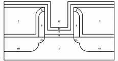
首先,参照图1,形成基础结构,也即在衬底上形成伪栅极堆叠结构、在伪栅极堆叠结构两侧的衬底中形成源漏区、在伪栅极堆叠结构两侧的衬底上形成栅极侧墙。提供衬底1,衬底1可以是体Si、绝缘层上Si(SOI)等常用的半导体硅基衬底,或者体Ge、绝缘体上Ge(GeOI),也可以是SiGe、GaAs、GaN、InSb、InAs等化合物半导体衬底,衬底的选择依据其上要制作的具体半导体器件的电学性能需要而设定。在本发明中,实施例所举的半导体器件例如为场效应晶体管(MOSFET),因此从与其他工艺兼容以及成本控制的角度考虑,优选体硅或SOI作为衬底1的材料。优选地,衬底1具有掺杂以形成阱区(未示出),例如PMOS器件中n衬底中的P-阱区。在衬底1上通过LPCVD、PECVD、HDPCVD、RTO等常规工艺沉积形成衬垫层2,其材质包括氮化物(例如Si3N4或SiNx,其中x为1~2)、氧化物(例如SiO或SiO2)或氮氧化物(例如SiON),并优选SiO2。衬垫层2用于稍后刻蚀的停止层,以保护衬底1,其厚度依照刻蚀工艺需要而设定。随后在衬垫层2上通过LPCVD、PECVD、HDPCVD、MBE、ALD、蒸发、溅射等常规工艺沉积形成伪栅极层3,其材质包括多晶硅、非晶硅、微晶硅、非晶碳、非晶锗等及其组合,用在后栅工艺中以便控制栅极形状。刻蚀衬垫层2与伪栅极层3,余下的堆叠结构构成伪栅极堆叠结构2/3。以伪栅极堆叠结构2/3为掩模,进行第一次源漏离子注入,在伪栅极堆叠结构两侧的衬底1中形成轻掺杂、浅pn结的源漏扩展区4L(也即LDD结构)。随后在整个器件表面沉积绝缘隔离材料并刻蚀,仅在伪栅极堆叠结构周围的衬底1上形成栅极侧墙5。栅极侧墙5的材质包括氮化物、氧化物、氮氧化物、DLC及其组合,其与衬垫层2和伪栅极层3材质均不同,便于选择性刻蚀。特别地,栅极侧墙5可以包括多层结构(未示出),例如具有垂直部分以及水平部分的剖面为L形的第一栅极侧墙,以及位于第一栅极侧墙水平部分上的高应力的第二栅极侧墙,第二栅极侧墙的材质可包括SiN或类金刚石无定形碳(DLC),应力优选大于2GPa。以栅极侧墙5为掩模,进行第二次源漏离子注入,在栅极侧墙5两侧的衬底1中形成重掺杂、深pn结的源漏重掺杂区4H。源漏扩展区4L与源漏重掺杂区4H共同构成MOSFET的源漏区4,其掺杂类型和浓度、深度依照MOSFET器件电学特性需要而定。First, referring to FIG. 1, the basic structure is formed, that is, a dummy gate stack structure is formed on the substrate, source and drain regions are formed in the substrate on both sides of the dummy gate stack structure, and substrates on both sides of the dummy gate stack structure are formed. Gate spacers are formed on the bottom. A
其次,参照图2,在整个器件上形成应力衬层。通过LPCVD、PECVD、HDPCVD、MBE、ALD、磁控溅射、磁过滤脉冲阴极真空弧放电(FCVA)技术等常规工艺,形成应力衬层6,覆盖了源漏区4、栅极侧墙5以及伪栅极层3。应力衬层6的材质可以是氧化硅、氮化硅、氮氧化硅、DLC及其组合。优选地,应力衬层6的材质是氮化硅,并且更优选地具有应力,其绝对值例如大于1GPa。对于PMOS而言,应力衬层6可以具有压应力,绝对值例如大于3GPa;对于NMOS而言,应力衬层6可以具有张应力,其绝对值例如大于2GPa。应力衬层6的厚度例如是10~1000nm。此外,层6还可以是DLC与氮化硅的组合,或者是掺杂有其他元素的氮化硅(例如掺杂C、F、S、P等其他元素以便提高氮化硅应力)。Next, referring to Figure 2, a stress liner is formed over the entire device. Through conventional processes such as LPCVD, PECVD, HDPCVD, MBE, ALD, magnetron sputtering, and magnetic filter pulse cathode vacuum arc discharge (FCVA) technology, the
参照图3,在整个器件上形成层间介质层(ILD)并且刻蚀露出应力衬层。通过旋涂、喷涂、丝网印刷、CVD等常规方法形成低k材料的ILD 7,其材质包括但不限于有机低k材料(例如含芳基或者多元环的有机聚合物)、无机低k材料(例如二氧化硅、无定形碳氮薄膜、多晶硼氮薄膜、氟硅玻璃、BSG、PSG、BPSG)、多孔低k材料(例如二硅三氧烷(SSQ)基多孔低k材料、多孔二氧化硅、多孔SiOCH、掺C二氧化硅、掺F多孔无定形碳、多孔金刚石、多孔有机聚合物)。采用回刻(湿法和/或干法刻蚀)、CMP等技术平坦化ILD 7和应力衬层6,直至暴露出伪栅极层3。Referring to FIG. 3, an interlayer dielectric layer (ILD) is formed on the entire device and etched to expose the stress liner. The ILD 7 of low-k materials is formed by conventional methods such as spin coating, spray coating, screen printing, and CVD, and its materials include but not limited to organic low-k materials (such as organic polymers containing aryl groups or polycyclic rings), inorganic low-k materials (e.g. silicon dioxide, amorphous carbon-nitride films, polycrystalline boron-nitride films, fluorosilicate glass, BSG, PSG, BPSG), porous low-k materials (e.g. disilatrioxane (SSQ)-based porous low-k materials, porous Silica, porous SiOCH, C-doped silica, F-doped porous amorphous carbon, porous diamond, porous organic polymer). Etching back (wet and/or dry etching), CMP and other technologies are used to planarize the ILD 7 and the
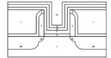
参照图4,去除伪栅极层3,留下栅极沟槽3T。对于多晶硅、非晶硅、微晶硅等Si基材质的伪栅极层3而言,可以采用TMAH湿法腐蚀,或者碳氟基气体等离子体干法刻蚀,去除伪栅极层3,直至露出衬垫层2,留下栅极侧墙5、应力衬层6和ILD 7包围的栅极沟槽3T。Referring to FIG. 4 , the
参照图5,在栅极沟槽3T中沉积形成界面层8。优选地,通过HF基湿法腐蚀液去除氧化硅材质的衬垫层2,并清洗、干燥暴露出的衬底1表面,以减小沟道区表面缺陷。随后,在衬底1上栅极沟槽3T中形成界面层8。界面层8材质是氧化硅,其形成方法可以是PECVD、HDPCVD、MBE、ALD等常规方法,还可以是化学氧化方法,例如在含有10ppm臭氧的去离子水中浸泡20s,使得硅材质的衬底1表面被氧化形成氧化硅的界面层8。该薄层界面层用于降低衬底1与未来高k材料的栅极绝缘层之间的界面态密度。Referring to FIG. 5 , an
参照图6,在ILD 7上以及栅极沟槽3T中形成高k材料的栅极绝缘层9。高k材料包括但不限于氮化物(例如SiN、AlN、TiN)、金属氧化物(主要为副族和镧系金属元素氧化物,例如Al2O3、Ta2O5、Ti O2、ZnO、ZrO2、HfO2、CeO2、Y2O3、La2O3)、钙钛矿相氧化物(例如PbZrxTi1-xO3(PZT)、BaxSr1-xTiO3(BST))。形成方法可以是CVD、PVD、ALD等常规方法。随后,采用沉积后退火(PDA),例如在450℃下退火15s,以提高HK材料的质量。Referring to FIG. 6 , a
参照图7,在栅极绝缘层9上沉积盖帽层10。沉积方法例如是CVD、PVD、ALD等,材质例如是TiN、TaN及其组合。盖帽层10可以阻挡上层的金属扩散到HK层9中。Referring to FIG. 7 , a
参照图8,在盖帽层10上形成栅极导电层11。栅极导电层11用于调整栅极功函数,对于NMOS而言可以选用Al、TiAl、对于PMOS而言可以选用Ti、TiN、Ta、TaN。沉积方法例如是CVD、PVD、ALD等。Referring to FIG. 8 , a gate
参照图9,在栅极导电层11上形成阻挡盖帽层12。形成方法例如是CVD、PVD、ALD等,其材质可以是TiN、TaN,用于调整金属栅极功函数以及势垒阻挡层。Referring to FIG. 9 , a blocking
参照图10,采用ALD法,在阻挡盖帽层12上形成金属W层13。Referring to FIG. 10, a
可选地,预热晶片,将晶片送入CVD反应室,加热至约200℃,提高整个晶片热量以促进分子运动,利于稍后的反应和沉积。Optionally, preheat the wafer, send the wafer into the CVD reaction chamber, heat it to about 200°C, increase the heat of the entire wafer to promote molecular movement, and facilitate later reaction and deposition.
可选地,在晶片上沉积薄硅层(未示出)。通入硅烷(SiH4)等含硅气体,分解从而在晶片表面沉积形成了薄硅层,例如为单原子Si层,该单原子层Si可以保护其下方的Ti、Ta、TiN、TaN等材质的阻挡层/粘附层免受稍后WF6的侵蚀。Optionally, a thin silicon layer (not shown) is deposited on the wafer. Pass through silicon-containing gas such as silane (SiH4 ), decompose and deposit a thin silicon layer on the surface of the wafer, such as a single-atom Si layer, which can protect the underlying Ti, Ta, TiN, TaN and other materials The barrier/adhesion layer protects against later WF6 attack.
采用原子层沉积(ALD)工艺,在晶片上形成W层13。ALD工艺的前驱物包括硼烷(B2H6)与氟化钨(WF6),工艺温度为250~350℃并且优选300℃。具体地,参照图2所示,在ALD沉积的循环周期内:WF6最先沉积在晶片表面(优选地包括薄Si层)形成第一层W单原子层,并且W-F链上F一侧朝向上;随后停止通入WF6转而通入B2H6,B和H取代了W-F链上的F;接着停止通入B2H6转而继续通入WF6,第一层W上方的B和H还原了通入的WF6从而形成了第二层W单原子层;然后停止WF6转而通入B2H6,B和H再次取代了第二层W单原子层顶部的F,此后周而复始,间歇地交替通入WF6和B2H6,最终形成了多个W单原子层,构成最终的W层。ALD工艺中,沉积速率例如是


在此ALD法步骤中形成的W层13,不同于以往CVD法制备的W层,台阶覆盖性有了显著提升,填洞的能力有效增强,有利于提高器件的可靠性。The
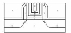
参照图11,采用CMP等方法,平坦化层9~13,直至暴露ILD 7。Referring to FIG. 11 , use methods such as CMP to planarize
参照图12,形成源漏接触硅化物。在ILD 7中刻蚀形成源漏接触孔7C,直至暴露源漏区4(4H)。在接触孔7C中沉积Ni、Pt、Co、Ti等金属及其组合,退火使得金属薄层与源漏区中的Si反应形成源漏接触金属硅化物14。随后湿法刻蚀去除未反应的金属薄层。Referring to FIG. 12 , a source-drain contact silicide is formed. Source and drain
参照图13,填充接触孔形成源漏接触。在接触孔7C中沉积1~7nm厚的TiN、TaN的阻挡层15,随后采用CVD或者ALD法沉积金属W、Al、Mo、Cu及其组合,形成源漏接触16。最后CMP或者回刻,直至暴露ILD7。Referring to FIG. 13 , the contact holes are filled to form source and drain contacts. A
最终形成的器件结构如图13所示,包括衬底上的栅极堆叠结构、栅极堆叠结构两侧衬底中的源漏区4、栅极堆叠结构两侧衬底上的栅极侧墙5,其特征在于栅极堆叠结构依次包括界面层8、高k的栅极绝缘层9、盖帽层10、栅极导电层11、阻挡盖帽层12以及金属W层13,其中金属W层13采用ALD法制备。对其余各个部件及其材料、几何参数在制造方法中已详细描述,在此不再赘述。The finally formed device structure is shown in Figure 13, including the gate stack structure on the substrate, the source and drain regions 4 in the substrates on both sides of the gate stack structure, and the gate spacers on the substrates on both sides of the gate stack structure. 5. It is characterized in that the gate stack structure sequentially includes an
依照本发明的半导体器件及其制造方法,采用ALD法在金属栅极顶部沉积W层,有效改善了金属栅极薄膜台阶覆盖性,提升了器件的可靠性。According to the semiconductor device and its manufacturing method of the present invention, the ALD method is used to deposit the W layer on the top of the metal gate, which effectively improves the step coverage of the metal gate film and improves the reliability of the device.
尽管已参照一个或多个示例性实施例说明本发明,本领域技术人员可以知晓无需脱离本发明范围而对器件结构和/或工艺流程做出各种合适的改变和等价方式。此外,由所公开的教导可做出许多可能适于特定情形或材料的修改而不脱离本发明范围。因此,本发明的目的不在于限定在作为用于实现本发明的最佳实施方式而公开的特定实施例,而所公开的器件结构及其制造方法将包括落入本发明范围内的所有实施例。Although the invention has been described with reference to one or more exemplary embodiments, those skilled in the art will recognize various suitable changes and equivalents in device structures and/or process flows without departing from the scope of the invention. In addition, many modifications, possibly suited to a particular situation or material, may be made from the disclosed teaching without departing from the scope of the invention. Therefore, it is intended that the invention not be limited to the particular embodiment disclosed as the best mode for carrying out this invention, but that the disclosed device structures and methods of making the same will include all embodiments falling within the scope of the invention .
Claims (10)

Priority Applications (1)
| Application Number | Priority Date | Filing Date | Title |
|---|---|---|---|
| CN201210424681.5ACN103794502A (en) | 2012-10-30 | 2012-10-30 | Semiconductor device and method for manufacturing the same |
Applications Claiming Priority (1)
| Application Number | Priority Date | Filing Date | Title |
|---|---|---|---|
| CN201210424681.5ACN103794502A (en) | 2012-10-30 | 2012-10-30 | Semiconductor device and method for manufacturing the same |
Publications (1)
| Publication Number | Publication Date |
|---|---|
| CN103794502Atrue CN103794502A (en) | 2014-05-14 |
Family
ID=50670049
Family Applications (1)
| Application Number | Title | Priority Date | Filing Date |
|---|---|---|---|
| CN201210424681.5APendingCN103794502A (en) | 2012-10-30 | 2012-10-30 | Semiconductor device and method for manufacturing the same |
Country Status (1)
| Country | Link |
|---|---|
| CN (1) | CN103794502A (en) |
Cited By (5)
| Publication number | Priority date | Publication date | Assignee | Title |
|---|---|---|---|---|
| CN105405764A (en)* | 2014-07-25 | 2016-03-16 | 中国科学院微电子研究所 | Semiconductor device manufacturing method |
| CN106257620A (en)* | 2015-06-18 | 2016-12-28 | 中芯国际集成电路制造(上海)有限公司 | A kind of semiconductor device and manufacture method, electronic installation |
| CN108493246A (en)* | 2018-02-09 | 2018-09-04 | 中国科学院微电子研究所 | Semiconductor device and method for manufacturing the same |
| CN108807378A (en)* | 2017-05-05 | 2018-11-13 | 中芯国际集成电路制造(上海)有限公司 | Fin field effect pipe and forming method thereof |
| CN110923659A (en)* | 2018-09-20 | 2020-03-27 | 东京毅力科创株式会社 | Film forming method and substrate processing system |
Citations (6)
| Publication number | Priority date | Publication date | Assignee | Title |
|---|---|---|---|---|
| KR100607756B1 (en)* | 2004-08-19 | 2006-08-01 | 동부일렉트로닉스 주식회사 | Tungsten contact electrode manufacturing method of semiconductor device |
| US20080081452A1 (en)* | 2006-09-29 | 2008-04-03 | Soo Hyun Kim | Method of forming tungsten polymetal gate having low resistance |
| US20090053893A1 (en)* | 2005-01-19 | 2009-02-26 | Amit Khandelwal | Atomic layer deposition of tungsten materials |
| CN101447427A (en)* | 2007-11-30 | 2009-06-03 | 海力士半导体有限公司 | Method for forming tungsten film and method for forming wiring of semiconductor device using the same |
| US20110241130A1 (en)* | 2010-04-02 | 2011-10-06 | Taiwan Semiconductor Manufacturing Company, Ltd. | Semiconductor device having a blocking structure and method of manufacturing the same |
| US20120119204A1 (en)* | 2010-11-17 | 2012-05-17 | International Business Machines Corporation | Replacement Gate Having Work Function at Valence Band Edge |
- 2012
- 2012-10-30CNCN201210424681.5Apatent/CN103794502A/enactivePending
Patent Citations (6)
| Publication number | Priority date | Publication date | Assignee | Title |
|---|---|---|---|---|
| KR100607756B1 (en)* | 2004-08-19 | 2006-08-01 | 동부일렉트로닉스 주식회사 | Tungsten contact electrode manufacturing method of semiconductor device |
| US20090053893A1 (en)* | 2005-01-19 | 2009-02-26 | Amit Khandelwal | Atomic layer deposition of tungsten materials |
| US20080081452A1 (en)* | 2006-09-29 | 2008-04-03 | Soo Hyun Kim | Method of forming tungsten polymetal gate having low resistance |
| CN101447427A (en)* | 2007-11-30 | 2009-06-03 | 海力士半导体有限公司 | Method for forming tungsten film and method for forming wiring of semiconductor device using the same |
| US20110241130A1 (en)* | 2010-04-02 | 2011-10-06 | Taiwan Semiconductor Manufacturing Company, Ltd. | Semiconductor device having a blocking structure and method of manufacturing the same |
| US20120119204A1 (en)* | 2010-11-17 | 2012-05-17 | International Business Machines Corporation | Replacement Gate Having Work Function at Valence Band Edge |
Cited By (7)
| Publication number | Priority date | Publication date | Assignee | Title |
|---|---|---|---|---|
| CN105405764A (en)* | 2014-07-25 | 2016-03-16 | 中国科学院微电子研究所 | Semiconductor device manufacturing method |
| CN105405764B (en)* | 2014-07-25 | 2018-07-31 | 中国科学院微电子研究所 | Semiconductor device manufacturing method |
| CN106257620A (en)* | 2015-06-18 | 2016-12-28 | 中芯国际集成电路制造(上海)有限公司 | A kind of semiconductor device and manufacture method, electronic installation |
| CN106257620B (en)* | 2015-06-18 | 2019-09-27 | 中芯国际集成电路制造(上海)有限公司 | A kind of semiconductor device and its manufacturing method, electronic device |
| CN108807378A (en)* | 2017-05-05 | 2018-11-13 | 中芯国际集成电路制造(上海)有限公司 | Fin field effect pipe and forming method thereof |
| CN108493246A (en)* | 2018-02-09 | 2018-09-04 | 中国科学院微电子研究所 | Semiconductor device and method for manufacturing the same |
| CN110923659A (en)* | 2018-09-20 | 2020-03-27 | 东京毅力科创株式会社 | Film forming method and substrate processing system |
Similar Documents
| Publication | Publication Date | Title |
|---|---|---|
| CN103390644B (en) | Semiconductor device and method for manufacturing the same | |
| KR102287552B1 (en) | Selective high-k formation in gate-last process | |
| CN105097474B (en) | Method for manufacturing semiconductor device | |
| CN103035712B (en) | Semiconductor device and method for manufacturing the same | |
| US20210296450A1 (en) | Semiconductor device and methods of manufacture | |
| US9029959B2 (en) | Composite high-k gate dielectric stack for reducing gate leakage | |
| US20150084132A1 (en) | Silicon Nitride Layer Deposited at Low Temperature to Prevent Gate Dielectric Regrowth High-K Metal Gate Field Effect Transistors | |
| CN107316809B (en) | Manufacturing method of semiconductor device, high-K dielectric structure and manufacturing method thereof | |
| CN103390556B (en) | Semiconductor device manufacturing method | |
| CN103794502A (en) | Semiconductor device and method for manufacturing the same | |
| CN104425575A (en) | Metal gate structure and manufacturing method thereof | |
| CN103839806B (en) | Semiconductor device and method for manufacturing the same | |
| CN104916538B (en) | Semiconductor device and manufacturing method thereof | |
| CN105336784B (en) | Semiconductor device and method for manufacturing the same | |
| CN104979181B (en) | Method for manufacturing semiconductor device | |
| CN104979277A (en) | Chemical mechanical planarization process method | |
| CN103681844A (en) | Semiconductor device and method for manufacturing the same | |
| CN105336619B (en) | Semiconductor device manufacturing method | |
| CN106504983B (en) | Semiconductor device manufacturing method | |
| TWI798543B (en) | Semiconductor device and method for manufacturing the same | |
| CN103515235A (en) | Method for manufacturing metal gate semiconductor device | |
| CN104952713A (en) | Method for manufacturing semiconductor device | |
| KR20060064887A (en) | Transistor Formation Method of Semiconductor Device |
Legal Events
| Date | Code | Title | Description |
|---|---|---|---|
| C06 | Publication | ||
| PB01 | Publication | ||
| C10 | Entry into substantive examination | ||
| SE01 | Entry into force of request for substantive examination | ||
| RJ01 | Rejection of invention patent application after publication | ||
| RJ01 | Rejection of invention patent application after publication | Application publication date:20140514 |