CN103765519A - Intelligent shifting of read pass voltages for non-volatile storage - Google Patents
Intelligent shifting of read pass voltages for non-volatile storageDownload PDFInfo
- Publication number
- CN103765519A CN103765519ACN201280027700.9ACN201280027700ACN103765519ACN 103765519 ACN103765519 ACN 103765519ACN 201280027700 ACN201280027700 ACN 201280027700ACN 103765519 ACN103765519 ACN 103765519A
- Authority
- CN
- China
- Prior art keywords
- voltage
- read
- program
- tube core
- memory
- Prior art date
- Legal status (The legal status is an assumption and is not a legal conclusion. Google has not performed a legal analysis and makes no representation as to the accuracy of the status listed.)
- Granted
Links
- 238000003860storageMethods0.000titleabstractdescription24
- 230000015654memoryEffects0.000claimsabstractdescription370
- 238000000034methodMethods0.000claimsdescription111
- 238000012360testing methodMethods0.000claimsdescription12
- 238000012795verificationMethods0.000claimsdescription11
- 125000004122cyclic groupChemical group0.000claimsdescription4
- 230000008569processEffects0.000description78
- 238000007667floatingMethods0.000description26
- 238000009826distributionMethods0.000description20
- 230000001351cycling effectEffects0.000description18
- 235000012431wafersNutrition0.000description15
- 238000012545processingMethods0.000description14
- 238000004519manufacturing processMethods0.000description10
- 238000012937correctionMethods0.000description8
- 238000010586diagramMethods0.000description7
- 230000006870functionEffects0.000description7
- 238000004891communicationMethods0.000description6
- 230000014759maintenance of locationEffects0.000description6
- 238000004088simulationMethods0.000description6
- 239000004065semiconductorSubstances0.000description5
- VYPSYNLAJGMNEJ-UHFFFAOYSA-Nsilicon dioxideInorganic materialsO=[Si]=OVYPSYNLAJGMNEJ-UHFFFAOYSA-N0.000description5
- 238000005516engineering processMethods0.000description4
- 230000004044responseEffects0.000description4
- 239000000758substrateSubstances0.000description4
- 230000006399behaviorEffects0.000description3
- 230000008859changeEffects0.000description3
- 230000005684electric fieldEffects0.000description3
- 238000007726management methodMethods0.000description3
- 150000004767nitridesChemical class0.000description3
- 230000008878couplingEffects0.000description2
- 238000010168coupling processMethods0.000description2
- 238000005859coupling reactionMethods0.000description2
- 238000013500data storageMethods0.000description2
- 238000013461designMethods0.000description2
- 238000002474experimental methodMethods0.000description2
- 238000012986modificationMethods0.000description2
- 230000004048modificationEffects0.000description2
- 235000012239silicon dioxideNutrition0.000description2
- 239000000377silicon dioxideSubstances0.000description2
- 229910052814silicon oxideInorganic materials0.000description2
- 238000012546transferMethods0.000description2
- 230000005689Fowler Nordheim tunnelingEffects0.000description1
- 229910052581Si3N4Inorganic materials0.000description1
- XUIMIQQOPSSXEZ-UHFFFAOYSA-NSiliconChemical compound[Si]XUIMIQQOPSSXEZ-UHFFFAOYSA-N0.000description1
- LPQOADBMXVRBNX-UHFFFAOYSA-Nac1ldcw0Chemical compoundCl.C1CN(C)CCN1C1=C(F)C=C2C(=O)C(C(O)=O)=CN3CCSC1=C32LPQOADBMXVRBNX-UHFFFAOYSA-N0.000description1
- PNEYBMLMFCGWSK-UHFFFAOYSA-Naluminium oxideInorganic materials[O-2].[O-2].[O-2].[Al+3].[Al+3]PNEYBMLMFCGWSK-UHFFFAOYSA-N0.000description1
- 238000004364calculation methodMethods0.000description1
- 239000003990capacitorSubstances0.000description1
- 230000001413cellular effectEffects0.000description1
- 229910052681coesiteInorganic materials0.000description1
- 229910052593corundumInorganic materials0.000description1
- 229910052906cristobaliteInorganic materials0.000description1
- 230000007547defectEffects0.000description1
- 230000002950deficientEffects0.000description1
- 239000003989dielectric materialSubstances0.000description1
- 238000009792diffusion processMethods0.000description1
- 230000000694effectsEffects0.000description1
- 238000009413insulationMethods0.000description1
- 210000004072lungAnatomy0.000description1
- 238000013507mappingMethods0.000description1
- 230000007246mechanismEffects0.000description1
- 230000002093peripheral effectEffects0.000description1
- 229910021420polycrystalline siliconInorganic materials0.000description1
- 229920005591polysiliconPolymers0.000description1
- 229910052710siliconInorganic materials0.000description1
- 239000010703siliconSubstances0.000description1
- HQVNEWCFYHHQES-UHFFFAOYSA-Nsilicon nitrideChemical compoundN12[Si]34N5[Si]62N3[Si]51N64HQVNEWCFYHHQES-UHFFFAOYSA-N0.000description1
- 229910052682stishoviteInorganic materials0.000description1
- 230000008685targetingEffects0.000description1
- 229910052905tridymiteInorganic materials0.000description1
- 238000010200validation analysisMethods0.000description1
- 229910001845yogo sapphireInorganic materials0.000description1
Images


Classifications
- G—PHYSICS
- G11—INFORMATION STORAGE
- G11C—STATIC STORES
- G11C16/00—Erasable programmable read-only memories
- G11C16/02—Erasable programmable read-only memories electrically programmable
- G11C16/06—Auxiliary circuits, e.g. for writing into memory
- G11C16/34—Determination of programming status, e.g. threshold voltage, overprogramming or underprogramming, retention
- G—PHYSICS
- G11—INFORMATION STORAGE
- G11C—STATIC STORES
- G11C16/00—Erasable programmable read-only memories
- G11C16/02—Erasable programmable read-only memories electrically programmable
- G11C16/06—Auxiliary circuits, e.g. for writing into memory
- G11C16/26—Sensing or reading circuits; Data output circuits
- G—PHYSICS
- G11—INFORMATION STORAGE
- G11C—STATIC STORES
- G11C16/00—Erasable programmable read-only memories
- G11C16/02—Erasable programmable read-only memories electrically programmable
- G11C16/06—Auxiliary circuits, e.g. for writing into memory
- G11C16/34—Determination of programming status, e.g. threshold voltage, overprogramming or underprogramming, retention
- G11C16/3436—Arrangements for verifying correct programming or erasure
- G11C16/3454—Arrangements for verifying correct programming or for detecting overprogrammed cells
- G—PHYSICS
- G11—INFORMATION STORAGE
- G11C—STATIC STORES
- G11C16/00—Erasable programmable read-only memories
- G11C16/02—Erasable programmable read-only memories electrically programmable
- G11C16/06—Auxiliary circuits, e.g. for writing into memory
- G11C16/34—Determination of programming status, e.g. threshold voltage, overprogramming or underprogramming, retention
- G11C16/349—Arrangements for evaluating degradation, retention or wearout, e.g. by counting erase cycles
- G—PHYSICS
- G11—INFORMATION STORAGE
- G11C—STATIC STORES
- G11C29/00—Checking stores for correct operation ; Subsequent repair; Testing stores during standby or offline operation
- G11C29/02—Detection or location of defective auxiliary circuits, e.g. defective refresh counters
- G11C29/021—Detection or location of defective auxiliary circuits, e.g. defective refresh counters in voltage or current generators
- G—PHYSICS
- G11—INFORMATION STORAGE
- G11C—STATIC STORES
- G11C29/00—Checking stores for correct operation ; Subsequent repair; Testing stores during standby or offline operation
- G11C29/02—Detection or location of defective auxiliary circuits, e.g. defective refresh counters
- G11C29/028—Detection or location of defective auxiliary circuits, e.g. defective refresh counters with adaption or trimming of parameters
- G—PHYSICS
- G11—INFORMATION STORAGE
- G11C—STATIC STORES
- G11C11/00—Digital stores characterised by the use of particular electric or magnetic storage elements; Storage elements therefor
- G11C11/56—Digital stores characterised by the use of particular electric or magnetic storage elements; Storage elements therefor using storage elements with more than two stable states represented by steps, e.g. of voltage, current, phase, frequency
- G11C11/5621—Digital stores characterised by the use of particular electric or magnetic storage elements; Storage elements therefor using storage elements with more than two stable states represented by steps, e.g. of voltage, current, phase, frequency using charge storage in a floating gate
- G11C11/5642—Sensing or reading circuits; Data output circuits
Landscapes
- Read Only Memory (AREA)
Abstract
Description
Translated fromChinese背景技术Background technique
技术领域technical field
本发明涉及非易失性存储技术。The present invention relates to non-volatile memory technology.
相关技术的描述Description of related technologies
在各种电子装置中使用半导体存储装置变得比较流行。例如,在蜂窝式电话、数码相机、个人数字助理、移动计算装置、非移动计算装置和其他装置中使用非易失性半导体存储器。电可擦可编程只读存储器(EEPROM)和快闪存储器属于非易失性半导体存储器中最流行的存储器。It has become popular to use semiconductor memory devices in various electronic devices. For example, non-volatile semiconductor memory is used in cellular telephones, digital cameras, personal digital assistants, mobile computing devices, non-mobile computing devices, and other devices. Electrically Erasable Programmable Read-Only Memory (EEPROM) and flash memory are among the most popular types of non-volatile semiconductor memory.
EEPROM和快闪存储器二者都利用了位于半导体基板中的沟道区域之上且与该沟道区域绝缘的浮置栅极。浮置栅极位于源极区域与漏极区域之间。控制栅极设置在浮置栅极之上且与浮置栅极绝缘。晶体管的阈值电压由留存在浮置栅极上的电荷量来控制。就是说,在接通晶体管以允许晶体管的源极与漏极之间导通之前必须施加到控制栅极的电压的最小量由浮置栅极上的电荷的水平来控制。Both EEPROM and flash memory utilize a floating gate positioned over and insulated from a channel region in a semiconductor substrate. The floating gate is located between the source region and the drain region. The control gate is disposed over and insulated from the floating gate. The threshold voltage of a transistor is controlled by the amount of charge remaining on the floating gate. That is, the minimum amount of voltage that must be applied to the control gate before the transistor is turned on to allow conduction between the transistor's source and drain is controlled by the level of charge on the floating gate.
当对EEPROM或快闪存储器装置进行编程时,通常将编程电压施加到控制栅极,并且位线接地。来自沟道的电子注入到浮置栅极中。当电子在浮置栅极中累积时,浮置栅极变成带负电荷,并且存储器单元的阈值电压升高,使得存储器单元处于编程状态。可以在标题为“Source Side SelfBoosting Technique For Non-Volatile Memory”的美国专利6,859,397和标题为“Detecting Over Programmed Memory”的美国专利6,917,542中找到关于编程的更多信息,这两个专利的全部内容通过引用合并于此。When programming an EEPROM or flash memory device, typically a programming voltage is applied to the control gate and the bit line is grounded. Electrons from the channel are injected into the floating gate. When electrons accumulate in the floating gate, the floating gate becomes negatively charged and the threshold voltage of the memory cell rises, placing the memory cell in a programmed state. More information on programming can be found in US Patent 6,859,397 entitled "Source Side SelfBoosting Technique For Non-Volatile Memory" and US Patent 6,917,542 entitled "Detecting Over Programmed Memory", both of which are incorporated by reference in their entirety merged here.
一些EEPROM和快闪存储器装置具有用于存储两个范围的电荷的浮置栅极,因此,可以在下述两个状态之间对存储器单元进行编程/擦除,即对应于数据“1”和数据“0”的擦除状态和编程状态。这样的装置被称为二进制装置或双状态装置。Some EEPROM and flash memory devices have a floating gate for storing two ranges of charge, therefore, the memory cell can be programmed/erased between two states corresponding to data "1" and data "0" for erased state and programmed state. Such devices are known as binary devices or two-state devices.
通过识别多个不同的被允许的阈值电压范围而实施多状态快闪存储器单元。每个不同的阈值电压范围对应于一组数据位的预定值。编程到存储器单元中的数据与存储器单元的阈值电压范围之间的具体关系取决于为存储器单元采用的数据编码方案。例如,美国专利6,222,762和美国专利申请公开2004/0255090描述了多状态快闪存储器单元的各种数据编码方案,这两个专利文献的全部内容通过引用合并于此。Multi-state flash memory cells are implemented by identifying multiple different allowed threshold voltage ranges. Each distinct threshold voltage range corresponds to a predetermined value for a set of data bits. The specific relationship between the data programmed into a memory cell and the threshold voltage range of the memory cell depends on the data encoding scheme employed for the memory cell. For example, US Patent 6,222,762 and US Patent Application Publication 2004/0255090, the entire contents of which are hereby incorporated by reference, describe various data encoding schemes for multi-state flash memory cells.
在一些实施方式中,施加到控制栅极的编程电压包括一系列脉冲,该一系列脉冲的量值随着各连续脉冲以预定步长(例如,0.2v、0.3v、0.4v或其他)增加。在脉冲之间,存储器系统将验证各个存储器单元是否达到了其各自的目标阈值电压范围。达到了其目标阈值电压范围的那些存储器单元将被锁定于未来的编程之外(例如,通过将位线电压提高到Vdd)。当所有存储器单元都达到了其目标阈值电压范围时,编程完成。In some implementations, the programming voltage applied to the control gate comprises a series of pulses that increase in magnitude with each successive pulse in predetermined steps (eg, 0.2v, 0.3v, 0.4v, or other) . Between pulses, the memory system will verify that individual memory cells have reached their respective target threshold voltage ranges. Those memory cells that have reached their target threshold voltage range will be locked out of future programming (eg, by raising the bit line voltage to Vdd). Programming is complete when all memory cells have reached their target threshold voltage range.
在一些情况下,随着非易失性存储装置经过许多编程和擦除循环,非易失性存储装置的性能和行为可能会发生变化。为了考量该变化,可以针对已被编程和擦除许多次的非易失性存储装置来优化各种操作参数。然而,针对已被编程和擦除许多次的非易失性存储装置而优化操作参数可导致累及未被编程和擦除许多次的非易失性存储装置的性能。In some cases, the performance and behavior of a non-volatile memory device may change as the non-volatile memory device goes through many program and erase cycles. To account for this variation, various operating parameters can be optimized for a non-volatile memory device that has been programmed and erased many times. However, optimizing operating parameters for a non-volatile storage device that has been programmed and erased many times can result in compromising the performance of a non-volatile storage device that has not been programmed and erased many times.
附图说明Description of drawings
图1是NAND(与非)串的俯视图;Figure 1 is a top view of a NAND (and not) string;
图2是NAND串的等效电路图;Fig. 2 is the equivalent circuit diagram of NAND string;
图3是非易失性存储器系统的框图;Figure 3 is a block diagram of a non-volatile memory system;
图4是描述了感测块的一个实施例的框图;Figure 4 is a block diagram depicting one embodiment of a sensing block;
图5是描述了存储器阵列的一个实施例的框图;Figure 5 is a block diagram depicting one embodiment of a memory array;
图6描述了数据页;Figure 6 describes the data page;
图7是描述了用于制造并使用非易失性存储系统的处理的一个实施例的流程图;Figure 7 is a flowchart describing one embodiment of a process for manufacturing and using a non-volatile memory system;
图8描述了示例性的一组阈值电压分布并且描述了用于编程非易失性存储器的处理;FIG. 8 depicts an exemplary set of threshold voltage distributions and depicts a process for programming a non-volatile memory;
图9描述了三个编程脉冲以及在编程脉冲之间施加的验证脉冲;Figure 9 depicts three programming pulses and a verify pulse applied between the programming pulses;
图10A至图10E示出了各种阈值电压分布并且描述了用于对非易失性存储器进行编程的处理;10A-10E illustrate various threshold voltage distributions and describe a process for programming non-volatile memory;
图11是描述了用于对非易失性存储器进行编程的处理的一个实施例的流程图;Figure 11 is a flowchart describing one embodiment of a process for programming non-volatile memory;
图12是描述了用于从非易失性存储器进行读取的处理的一个实施例的流程图;Figure 12 is a flowchart describing one embodiment of a process for reading from non-volatile memory;
图13是描述了用于确定读取通过电压的各种实施例的图表;Figure 13 is a graph depicting various embodiments for determining a read pass voltage;
图14是具有多于一个管芯(die)的存储器系统的框图;Figure 14 is a block diagram of a memory system having more than one die;
图15描述了三个NAND串的一部分;Figure 15 depicts a portion of three NAND strings;
图16是描述了用于制造及配置非易失性存储器系统的处理的一个实施例的流程图;Figure 16 is a flowchart describing one embodiment of a process for fabricating and configuring a non-volatile memory system;
图17是描述了用于确定针对循环存储器(cycled memory)而优化的读取通过电压的处理的一个实施例的流程图;以及17 is a flowchart describing one embodiment of a process for determining a read pass voltage optimized for a cycled memory; and
图18是描述了用于确定针对新存储器(fresh memory)而优化的读取通过电压的处理的一个实施例的流程图。FIG. 18 is a flowchart describing one embodiment of a process for determining a read pass voltage optimized for fresh memory.
具体实施方式Detailed ways
在一些非易失性存储器的读取和验证操作期间,将未被选择的字线(例如,没有连接到被选择为要被读取的存储器单元的那些字线)提高到读取通过电压(例如,5伏特至10伏特)以使得存储器单元作为通过栅极而操作。被选择的字线连接到下述电压:针对每个读取和验证操作而指定该电压的水平,以确定相关存储器单元的阈值电压是否达到了该水平。因为未被选择的字线接收到读取通过电压,所以在读取操作期间具有较低阈值电压的、沿着未被选择的字线的存储器单元将在其控制栅极上接收一定电压,随着时间流逝该电压可能导致电子注入到其浮置栅极中。将电子注入到浮置栅极中将提高这些存储器单元的阈值电压。接收到读取通过电压的、已经被编程到与较高阈值电压相对应的状态的存储器单元可随着时间流逝而经历电子从浮置栅极移动到控制栅极,这降低了阈值电压。经验表明,如果存储器单元经历许多次读取操作而没有编程或擦除操作,则阈值电压可以如上所述随着时间流逝而发生改变。这种行为称为读取干扰(Read Disturb)。During read and verify operations of some nonvolatile memories, unselected word lines (eg, those word lines not connected to memory cells selected to be read) are raised to the read pass voltage ( For example, 5 volts to 10 volts) to cause the memory cell to operate as a pass gate. The selected word line is connected to a voltage whose level is specified for each read and verify operation to determine whether the threshold voltage of the associated memory cell has reached that level. Because the unselected word lines receive the read pass voltage, the memory cells along the unselected word lines that have lower threshold voltages during the read operation will receive a certain voltage on their control gates, followed by Over time this voltage can cause electrons to be injected into its floating gate. Injecting electrons into the floating gate will raise the threshold voltage of these memory cells. A memory cell that has received a read pass voltage that has been programmed to a state corresponding to a higher threshold voltage may experience electron movement from the floating gate to the control gate over time, which lowers the threshold voltage. Experience has shown that if a memory cell undergoes many read operations without programming or erasing operations, the threshold voltage can change over time as described above. This behavior is called Read Disturb.
已经观察到新存储器比循环存储器更易于受读取干扰的影响。新存储器或在新状况下的存储器指的是没有经历许多次编程/擦除循环的存储器。循环存储器或在循环状况下的存储器指的是经历过许多次编程/擦除循环的存储器。在一个示例中,当存储器经历过了100次编程/擦除循环时,存储器在循环状况下。编程/擦除循环是对存储器单元进行擦除和对存储器单元进行编程的组合。一种理论是,循环存储器具有在控制栅极与浮置栅极之间的绝缘中捕获的电子,这些电子减小了由读取通过电压形成的电场。因为电场减小,所以对于循环存储器减少了不想要的电子移动。这种行为表明较低的读取通过电压将减少读取干扰。It has been observed that new memory is more susceptible to read disturb than circular memory. Fresh memory, or memory in new condition, refers to memory that has not been through many program/erase cycles. Cyclic memory or memory under cycling conditions refers to memory that has undergone many program/erase cycles. In one example, a memory is in a cycled condition when the memory has undergone 100 program/erase cycles. A program/erase cycle is a combination of erasing and programming memory cells. One theory is that cycling memory has electrons trapped in the insulation between the control gate and the floating gate, which reduce the electric field created by the read pass voltage. Because the electric field is reduced, unwanted electron movement is reduced for cyclic memories. This behavior suggests that lower read pass voltages will reduce read disturb.
由于非易失性存储经历许多次编程/擦除循环,所以一些存储器单元可能经历编程噪声和/或数据留存问题。如上所述,通过识别多个不同的被允许的阈值电压范围而实施多状态非易失性存储器。每个不同的阈值电压范围对应于一组数据位的预定值。随着时间流逝,不同的被允许的阈值电压范围可能变宽而且区别变小,这称作为编程噪声。As non-volatile storage goes through many program/erase cycles, some memory cells may experience program noise and/or data retention issues. As described above, multi-state non-volatile memory is implemented by identifying multiple different allowable threshold voltage ranges. Each distinct threshold voltage range corresponds to a predetermined value for a set of data bits. Over time, the different allowed threshold voltage ranges may become wider and less distinct, which is referred to as programming noise.
另外,在许多次编程和擦除循环后,一些非易失性存储器将在存储器单元没有被擦除、编程或读取的情况下经历电子从浮置栅极离开。这将导致存储器单元的阈值电压发生漂移,这可能导致数据留存问题。Additionally, after many program and erase cycles, some non-volatile memories will experience electron exit from the floating gate without the memory cell being erased, programmed or read. This causes the threshold voltage of the memory cell to drift, which can lead to data retention issues.
高读取通过电压可以用于克服编程噪声和数据留存问题。通过使用较高的读取通过电压,即使存在编程噪声和/或数据留存问题,系统也可以更加容易地辨别多个不同的允许的阈值电压范围。然而,使用较高的读取通过电压来解决循环存储器的编程噪声和数据留存可能使新存储器的读取干扰恶化。因此,提议实施一种随着时间而改变读取通过电压的非易失性存储系统。新存储器将使用较低读取通过电压,而循环存储器将使用较高读取通过电压。A high read pass voltage can be used to overcome programming noise and data retention issues. By using a higher read pass voltage, the system can more easily discern between multiple different allowed threshold voltage ranges even in the presence of programming noise and/or data retention issues. However, using higher read pass voltages to address program noise and data retention for cycled memory may worsen read disturb for new memory. Therefore, it is proposed to implement a non-volatile memory system that changes the read pass voltage over time. New memories will use lower read pass voltages, while cycled memories will use higher read pass voltages.
在一个实施例中,系统将基于模拟、测试和/或实验来确定针对循环存储器而优化的读取通过电压和针对新存储器而优化的读取通过电压。可以针对整个晶片、单个管芯、单个块或其他单元来确定读取通过电压。在一些实施例中,确定针对新存储器而优化的读取通过电压,使得使用针对新存储器而优化的读取通过电压的新管芯的失败位的数目处于由对于新状况下的管芯使用针对循环存储器而优化的读取通过电压所导致的失败位的数目的预定百分比内。在一些实施例中,针对整个晶片(或管芯的另一集合)确定针对循环存储器而优化的读取通过电压,并且针对单个管芯(或单个块或其他单元)确定针对新存储器而优化的读取通过电压。In one embodiment, the system will determine an optimized read pass voltage for cycled memory and an optimized read pass voltage for new memory based on simulations, testing, and/or experimentation. The read pass voltage can be determined for an entire wafer, a single die, a single block, or other units. In some embodiments, the read pass voltage optimized for the new memory is determined such that the number of failed bits for a new die using the read pass voltage optimized for the new memory is within the range determined for the die usage for the new condition. Cycling the memory while optimizing the read pass voltage results in a predetermined percentage of the number of failed bits. In some embodiments, a read pass voltage optimized for cycling memory is determined for an entire wafer (or another collection of dies), and a read pass voltage optimized for new memory is determined for a single die (or a single block or other unit). Read pass voltage.
非易失性存储系统将被配置成监视存储器所经历过的编程/擦除循环的次数。可以针对整个系统、单个管芯、单个块或其他单位来监视编程/擦除循环的次数。当需要进行读取处理时,系统(例如,控制器、状态机或其他组件)将获得编程/擦除循环的计数,并基于编程/擦除循环的计数、针对循环存储器而优化的读取通过电压和针对新存储器而优化的读取通过电压来动态确定当前读取通过电压以用于该读取处理。A non-volatile memory system will be configured to monitor the number of program/erase cycles the memory has undergone. The number of program/erase cycles can be monitored for the entire system, a single die, a single block, or other units. When a read transaction is required, the system (e.g., a controller, state machine, or other component) obtains a count of program/erase cycles and, based on the count of program/erase cycles, reads optimized for cycling memory through The current read pass voltage is dynamically determined for the read process using the voltage and the read pass voltage optimized for the new memory.
这个动态确定的当前读取通过电压将被施加到未被选择的字线。在一个实施例中,当前读取通过电压将被施加到被选择的字线的一侧和/或两侧上的多个未被选择的字线,同时将读取比较电压施加到被选择的字线,以使得从被选择的存储器单元读取数据。在一些实施例中,紧挨着被选择的字线的字线可以接收不同的通过电压。This dynamically determined current read pass voltage will be applied to the unselected word lines. In one embodiment, the current read pass voltage will be applied to multiple unselected word lines on one and/or both sides of the selected word line, while the read compare voltage is applied to the selected word line. word line so that data is read from the selected memory cell. In some embodiments, word lines next to the selected word line may receive different pass voltages.
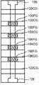
可以实施本文中所描述的技术的非易失性存储系统的一个示例是使用NAND结构的快闪存储器系统,该NAND结构包括串联布置多个晶体管,这些晶体管夹置在两个选择栅极之间。串联的晶体管以及选择栅极被称为NAND串。图1是示出了一个NAND串的俯视图。图2是NAND串的等效电路。在图1和图2中所描述的NAND串包括串联的且夹置在(漏极侧)选择栅极120与(源极侧)选择栅极122之间的四个晶体管100、102、104及106。选择栅极120将NAND串经由位线接触件126连接到位线。选择栅极122将NAND串连接到源极线128。通过将合适的电压施加到选择线SGD来控制选择栅极120。通过将合适的电压施加到选择线SGS来控制选择栅极122。晶体管100、102、104及106中的每一个都具有控制栅极和浮置栅极。例如,晶体管100具有控制栅极100CG和浮置栅极100FG。晶体管102包括控制栅极102CG和浮置栅极102FG。晶体管104包括控制栅极104CG和浮置栅极104FG。晶体管106包括控制栅极106CG和浮置栅极106FG。控制栅极100CG连接到字线WL3,控制栅极102CG连接到字线WL2,控制栅极104CG连接到字线WL1,而控制栅极106CG连接到字线WL0。One example of a non-volatile memory system that may implement the techniques described herein is a flash memory system that uses a NAND structure that includes a series arrangement of multiple transistors sandwiched between two select gates . Connecting transistors and select gates in series is called a NAND string. FIG. 1 is a top view showing one NAND string. Figure 2 is the equivalent circuit of a NAND string. The NAND string depicted in FIGS. 1 and 2 includes four
注意,虽然图1和图2示出了NAND串中的四个存储器单元,但仅作为示例而提供了四个存储器单元的使用。NAND串可以具有少于四个存储器单元或多于四个存储器单元。例如,一些NAND串将包括8个存储器单元、16个存储器单元、32个存储器单元、64个存储器单元、128个存储器单元等。这里的讨论不限于NAND串中的任何特定数目的存储器单元。一个实施例使用具有66个存储器单元的NAND串,其中,64个存储器单元用于存储数据,并且存储器单元中的两个存储器单元因为其不存储数据而被称为虚设存储器单元。Note that although Figures 1 and 2 show four memory cells in a NAND string, the use of four memory cells is provided as an example only. A NAND string can have less than four memory cells or more than four memory cells. For example, some NAND strings will include 8 memory cells, 16 memory cells, 32 memory cells, 64 memory cells, 128 memory cells, etc. The discussion here is not limited to any particular number of memory cells in a NAND string. One embodiment uses a NAND string with 66 memory cells, where 64 memory cells are used to store data, and two of the memory cells are called dummy memory cells because they do not store data.
使用NAND结构的快闪存储器系统的典型架构将包括若干NAND串。每个NAND串通过由选择线SGS控制的该NAND串的源极选择栅极而连接到共同源极线,并通过由选择线SGD控制的该NAND串的漏极选择栅极而连接到相关联的位线。每条位线和经由位线接触件连接到该位线的相应NAND串构成存储器单元阵列的列。多个NAND串共享位线。通常,位线在NAND串的顶部在与字线垂直的方向上延伸且连接到感测放大器。A typical architecture for a flash memory system using a NAND structure will include several NAND strings. Each NAND string is connected to a common source line through the source select gate of that NAND string, controlled by select line SGS, and to the associated NAND string through its drain select gate, controlled by select line SGD. the bit line. Each bit line and a corresponding NAND string connected to that bit line via a bit line contact constitutes a column of the memory cell array. Multiple NAND strings share bit lines. Typically, the bit lines run on top of the NAND strings in a direction perpendicular to the word lines and are connected to sense amplifiers.
在以下美国专利/专利申请中提供NAND型快闪存储器及其操作的相关示例,所有这些美国专利/专利申请的全部内容通过引用并入本文中:美国专利5,570,315、美国专利5,774,397、美国专利6,046,935、美国专利6,456,528和美国专利公开US2003/0002348。Related examples of NAND-type flash memory and its operation are provided in the following U.S. patents/patent applications, all of which are incorporated herein by reference in their entirety: U.S. Patent 5,570,315, U.S. Patent 5,774,397, U.S. Patent 6,046,935, US Patent 6,456,528 and US Patent Publication US2003/0002348.
除了NAND快闪存储器之外,其他类型的非易失性存储装置也可以用于实施本文中描述的新技术。例如,TANOS结构(由硅基板上的TaN-Al2O3-SiN-SiO2的堆叠层组成)也可以与本文中所描述的技术一起使用,该TANOS结构基本上是使用氮化物层(而不是浮置栅极)中的电荷捕获的存储器单元。在快闪EEPROM系统中有用的另一类型的存储器单元利用非导电介电材料取代导电的浮置栅极来以非易失性方式存储电荷。在1987年3月IEEE Electron Device Letters第EDL-8卷第3号第93-95页Chan等人的文章“A True Single-Transistor Oxide-Nitride-OxideEEPROM Device”中描述了这种存储器单元。由氧化硅、氮化硅和氧化硅(“ONO”)形成的三层介电质夹置在导电的控制栅极与存储器单元沟道之上的半导电基板的表面之间。存储器单元通过将来自单元沟道的电子注入到氮化物中而被编程,在氮化物中这些电子被捕获并存储在受限区域中。然后,该存储的电荷以可检测的方式改变单元的沟道的一部分的阈值电压。通过将热空穴注入到氮化物中来擦除单元。还参阅1991年4月IEEEJournal of Solid-State Circuits第26卷第4号第497-501页Nozaki等人的“A l-Mb EEPROM with MONOS Memory Cell for Semiconductor DiskApplication”,该文章描述了分裂栅极配置中的类似的存储器单元,其中参杂的多晶硅栅极延伸到存储器单元沟道的一部分上以形成分离的选择晶体管。In addition to NAND flash memory, other types of non-volatile storage devices can also be used to implement the new techniques described herein. For example, a TANOS structure (consisting of stacked layers of TaN-Al2O3 -SiN-SiO2 on a silicon substrate) can also be used with the technique described in this paper, which basically uses nitride layers (and not a floating gate) in a charge-trapped memory cell. Another type of memory cell useful in flash EEPROM systems utilizes a non-conductive dielectric material instead of a conductive floating gate to store charge in a non-volatile manner. Such a memory cell is described in the article "A True Single-Transistor Oxide-Nitride-Oxide EEPROM Device" by Chan et al., IEEE Electron Device Letters, Vol. EDL-8, No. 3, pp. 93-95, March 1987. A three-layer dielectric formed of silicon oxide, silicon nitride, and silicon oxide ("ONO") is sandwiched between the conductive control gate and the surface of the semiconductive substrate above the memory cell channel. The memory cell is programmed by injecting electrons from the cell channel into the nitride where they are trapped and stored in a confined area. This stored charge then detectably alters the threshold voltage of a portion of the cell's channel. The cell is erased by injecting hot holes into the nitride. See also "A l-Mb EEPROM with MONOS Memory Cell for Semiconductor Disk Application" by Nozaki et al., IEEE Journal of Solid-State Circuits Vol. 26 No. 4, April 1991, pp. 497-501, which describes the split-gate configuration A similar memory cell in , where the doped polysilicon gate extends over a portion of the memory cell channel to form a separate select transistor.
2000年11月IEEE Electron Device Letters第21卷第11号第543-545页Eitan等人的“NROM:A Novel Localized Trapping,2-Bit NonvolatileMemory Cell”描述了另一示例。ONO介电层延伸横过源极与漏极扩散之间的沟道。一个数据位的电荷位于与漏极相邻的介电层中,并且另一数据位的电荷位于与源极相邻的介电层中。美国专利5,768,192和6,011,725公开了一种具有夹置在两个二氧化硅层之间的捕获介电质的非易失性存储器单元。通过分别读取介电质内在空间上分离的各电荷存储区域的二进制状态而实施多状态数据存储。还可以使用其他类型的非易失性存储器技术。Another example is described in "NROM: A Novel Localized Trapping, 2-Bit Nonvolatile Memory Cell" by Eitan et al., IEEE Electron Device Letters, Vol. 21, No. 11, pp. 543-545, Nov. 2000. The ONO dielectric layer extends across the channel between the source and drain diffusions. The charge for one data bit is located in the dielectric layer adjacent to the drain, and the charge for the other data bit is located in the dielectric layer adjacent to the source. US Patents 5,768,192 and 6,011,725 disclose a non-volatile memory cell with a trapping dielectric sandwiched between two silicon dioxide layers. Multi-state data storage is implemented by separately reading the binary states of spatially separated charge storage regions within the dielectric. Other types of non-volatile memory technologies may also be used.
图3示出了具有读取/写入电路的存储器装置210,其中读取/写入电路用于并行地对存储器单元(例如,NAND多状态快闪存储器)的页进行读取和编程。存储器装置210可以包括一个或更多个存储器管芯或芯片212。存储器管芯212包括存储器单元的阵列(二维的或三维的)200、控制电路220以及读取/写入电路230A和230B。在一个实施例中,在存储器阵列200的相对侧上以对称方式实施由各种外围电路对该阵列的访问,以使得每一侧上的访问线和电路的密度减少一半。读取/写入电路230A和230B包括允许并行读取或编程存储器单元的页的多个感测块300。可经由行解码器240A和240B通过字线并且经由列解码器242A和242B通过位线而寻址存储器阵列200。在典型的实施例中,控制器244作为一个或更多个存储器管芯212而包括在同一存储器装置210(例如,可移除的存储卡或封装件)中。在主机与控制器244之间经由线232传输命令和数据,并且在控制器与一个或更多个存储器管芯212之间经由线234传输命令和数据。一些存储器系统可以包括与控制器244通信的多个管芯212。FIG. 3 shows a memory device 210 with read/write circuitry for reading and programming a page of memory cells (eg, NAND multi-state flash memory) in parallel. Memory device 210 may include one or more memory dies or chips 212 . Memory die 212 includes an array (two-dimensional or three-dimensional) of
控制电路220与读取/写入电路230A和230B协作,以对存储器阵列200进行存储器操作。控制电路220包括状态机222、片上地址解码器224及功率控制模块226。状态机222提供存储器操作的芯片级控制。片上地址解码器224提供在由主机或存储器控制器所使用的地址到由解码器240A、240B、242A和242B所使用的硬件地址之间的地址接口。功率控制模块226控制在存储器操作期间供应给字线和位线的功率和电压。在一个实施例中,功率控制模块226包括能够产生比电源电压更大的电压的一个或更多个电荷泵。控制电路220、功率控制模块226、解码器224、状态机222、解码器240A/240B和242A/242B、读取/写入电路230A/230B和控制器244可以统称为或分别称为一个或更多个管理电路。Control circuit 220 cooperates with read/write circuits 230A and 230B to perform memory operations on
图4是被划分成核心部分(称为感测模块480)以及共同部分490的单个感测块300的框图。在一个实施例中,对于每条位线存在单独的感测模块480,并且对于一组多个感测模块480存在一个共同部分490。在一个示例中,感测块包括一个共同部分490和八个感测模块480。一个群组中的感测模块中的每一个经由数据总线472与相关联的共同部分通信。对于更多细节,请参考美国专利申请公开2006/0140007,该案的全部内容通过引用合并于此。FIG. 4 is a block diagram of a single sensing block 300 divided into a core part, referred to as a sensing module 480 , and a common part 490 . In one embodiment, there is a separate sense module 480 for each bit line, and there is one common portion 490 for a set of multiple sense modules 480 . In one example, the sensing block includes one common portion 490 and eight sensing modules 480 . Each of the sensing modules in a group communicates with the associated common part via the data bus 472 . For more details, please refer to US Patent Application Publication 2006/0140007, which is hereby incorporated by reference in its entirety.
感测模块480包括用于确定所连接的位线中的传导电流是高于还是低于预定阈值水平的感测电路470。在一些实施例中,感测模块480包括通常被称为感测放大器的电路。感测模块480还包括用于设置所连接的位线上的电压状况的位线锁存器482。例如,在位线锁存器482中所锁存的预定状态将导致所连接的位线被拉至指明禁止编程的状态(例如,Vdd)。The sense module 480 includes a sense circuit 470 for determining whether the conduction current in the connected bit line is above or below a predetermined threshold level. In some embodiments, the sense module 480 includes a circuit commonly referred to as a sense amplifier. The sense module 480 also includes a bit line latch 482 for setting the voltage condition on the connected bit line. For example, a predetermined state latched in bit line latch 482 will cause the connected bit line to be pulled to a state (eg, Vdd) designating a program inhibit.
共同部分490包括处理器492、一组数据锁存器494及耦合在该组数据锁存器494与数据总线420之间的I/O接口496。处理器492进行计算。例如,处理器492的一个功能是确定存储在所感测的存储器单元中的数据并将所确定的数据存储在该组数据锁存器中。该组数据锁存器494用于存储在读取操作期间由处理器492所确定的数据位。该组数据锁存器494还用于存储在编程操作期间从数据总线420引入的数据位。所引入的数据位表示要被编程到存储器中的写入数据。I/O接口496在数据锁存器494与数据总线420之间提供接口。Common portion 490 includes a processor 492 , a set of data latches 494 , and an I/O interface 496 coupled between the set of data latches 494 and data bus 420 . Processor 492 performs calculations. For example, one function of processor 492 is to determine the data stored in the sensed memory cell and store the determined data in the set of data latches. The set of data latches 494 is used to store data bits determined by the processor 492 during a read operation. The set of data latches 494 is also used to store data bits introduced from the data bus 420 during programming operations. The data bits introduced represent the write data to be programmed into the memory. I/O interface 496 provides an interface between data latch 494 and data bus 420 .
在读取或感测期间,系统的操作受控于状态机222,该状态机222控制将不同的控制栅极电压供应给所寻址的单元。随着步进通过与存储器所支持的各种存储器状态相对应的各种预定义控制栅极电压(读取参考电压或验证参考电压),感测模块480可以在这些电压中的一个电压处跳脱(trip),并且输出将会从感测模块480经由总线472提供到处理器492。此时,处理器492通过考虑感测模块的跳脱事件和关于经由输入线493从状态机施加的控制栅极电压的信息来确定所得的存储器状态。然后,其计算存储器状态的二进制编码并将所得的数据位存储到数据锁存器494中。在核心部分的另一实施例中,位线锁存器482具有双重任务:既作为用于对感测模块480的输出进行锁存的锁存器,并且还作为如上所述的位线锁存器。During reading or sensing, the operation of the system is controlled by a state machine 222 which controls the supply of different control gate voltages to the addressed cells. As it steps through various predefined control gate voltages (either a read reference voltage or a verify reference voltage) corresponding to the various memory states supported by the memory, the sense module 480 may trip at one of these voltages trip, and the output will be provided from the sensing module 480 to the processor 492 via the bus 472 . At this point, processor 492 determines the resulting memory state by taking into account the trip event of the sense module and information about the control gate voltage applied from the state machine via input line 493 . It then computes the binary encoding of the memory state and stores the resulting data bits into data latches 494 . In another embodiment of the core part, the bit line latch 482 has double duty: as a latch for latching the output of the sense module 480, and also as a bit line latch as described above. device.
预期一些实施方式将包括多个处理器492。在一个实施例中,每个处理器492包括输出线(在图4中没有示出),使得每一条输出线“线或”(wired-OR)在一起。在一些实施例中,输出线在连接到线或线之前反转。在针对何时已完成编程处理的编程验证处理期间,该配置能够进行快速确定,这是因为接收线或线的状态机可以确定所有被编程的位何时达到了想要的水平。例如,当每个位达到了其想要的水平时,将该位的逻辑0发送给线或线(或将数据1反转)。当所有位输出数据0(或反转的数据1)时,于是,状态机知道要终止编程处理。在每个处理器与八个感测模块通信的实施例中,状态机可能(在后面的实施例中)需要读取线或线八次,或者逻辑被添加到处理器492以累积相关联的位线的结果,使得状态机仅需要读取线或线一次。在具有许多感测模块的一些实施例中,许多感测模块的线或线可以分群组在有N个感测模块的组中,然后,该群组可以被分组以形成二叉树。It is contemplated that some implementations will include multiple processors 492 . In one embodiment, each processor 492 includes output lines (not shown in FIG. 4 ) such that each output line is "wired-ORed" together. In some embodiments, the output lines are inverted before being connected to the OR line. This configuration enables a quick determination during the program verify process of when the program process has completed because the state machine receiving the wire-OR can determine when all programmed bits have reached the desired level. For example, when each bit has reached its desired level, sending a
在编程或验证期间,来自数据总线420的要编程的数据存储在该组数据锁存器494中。在状态机的控制下,编程操作包括同时施加到所寻址的存储器单元的控制栅极的一系列编程电压脉冲(具有增加的量值),使得这些存储器单元同时被编程。每个编程脉冲后接着验证处理,以确定存储器单元是否被编程到了想要的状态。处理器492相对于想要的存储器状态来监视所验证的存储器状态。当两者一致时,处理器492设置位线锁存器482以导致位线被拉至指明禁止编程的状态。这禁止了耦接到位线的存储器单元进一步编程,即使该存储器单元在其控制栅极上经受编程脉冲时也是如此。在其他实施例中,处理器初始加载位线锁存器482并且感测电路在验证处理期间将其设置成禁止值。Data to be programmed from the data bus 420 is stored in the set of data latches 494 during programming or verifying. Under the control of the state machine, a programming operation consists of a series of programming voltage pulses (of increasing magnitude) applied simultaneously to the control gates of addressed memory cells such that these memory cells are programmed simultaneously. Each programming pulse is followed by a verify process to determine whether the memory cell was programmed to the desired state. Processor 492 monitors the verified memory state relative to the desired memory state. When both match, processor 492 sets bit line latch 482 to cause the bit line to be pulled to a state indicating program inhibit. This inhibits further programming of the memory cell coupled to the bit line, even when the memory cell is subjected to a programming pulse on its control gate. In other embodiments, the processor initially loads the bit line latch 482 and the sense circuit sets it to an inhibit value during the verify process.
数据锁存堆栈494包含对应于感测模块的数据锁存器的堆栈。在一个实施例中,对于每个感测模块480有三个(或四个或另一数目的)数据锁存器。在一些实施例中(但非必要),数据锁存器实施为移位寄存器,以使得存储在该移位寄存器中的并行数据转换成用于数据总线420的串行数据,并且反之亦然。在一个优选的实施例中,对应于存储器单元的读取/写入块的所有数据锁存器可以链接在一起以形成块移位寄存器,以使得可以通过串行传输而输入或输出数据块。具体地,对读取/写入模块的库进行调整,使得其数据锁存器组中的每一个数据锁存器按序列将数据移至数据总线或将数据从数据总线移出,如同这些数据锁存器是整个读取/写入块的移位寄存器的一部分一样。Data latch stack 494 contains a stack of data latches corresponding to a sense module. In one embodiment, there are three (or four or another number) data latches for each sense module 480 . In some embodiments, but not necessarily, the data latches are implemented as shift registers such that parallel data stored in the shift registers is converted to serial data for data bus 420 and vice versa. In a preferred embodiment, all data latches corresponding to a read/write block of memory cells can be linked together to form a block shift register so that a block of data can be input or output by serial transfer. Specifically, the read/write module's bank is tuned so that each data latch in its data latch bank shifts data to or from the data bus in sequence, as the data latches The register is part of the shift register for the entire read/write block.
关于非易失性存储装置的各种实施例的结构和/或操作的另外的信息可以在以下中找到:(1)2004年3月25日公布的美国专利申请公开2004/0057287“Non-Volatile Memory And Method With Reduced SourceLine Bias Errors”;(2)2004年6月10日公布的美国专利申请公开2004/0109357“Non-Volatile Memory And Method with ImprovedSensing”;(3)美国专利申请公开20050169082;(4)发明人Jian Chen在2005年4月5日提交的标题为“Compensating for Coupling DuringRead Operations of Non-Volatile Memory”的美国专利申请公开2006/0221692;以及(5)发明人Siu Lung Chan和Raul-Adrian Cernea在2005年12月28日提交的标题为“Reference Sense Amplifier ForNon-Volatile Memory的美国专利申请公开2006/0158947。所有五个直接上面列出的专利文献的全部内容通过引用合并于此。Additional information regarding the structure and/or operation of various embodiments of non-volatile memory devices can be found in: (1) U.S. Patent Application Publication 2004/0057287 "Non-Volatile Memory And Method With Reduced SourceLine Bias Errors"; (2) US Patent Application Publication 2004/0109357 "Non-Volatile Memory And Method with ImprovedSensing" published on June 10, 2004; (3) US Patent Application Publication 20050169082; (4 ) U.S. Patent Application Publication 2006/0221692, filed April 5, 2005, titled "Compensating for Coupling During Read Operations of Non-Volatile Memory" by Jian Chen, inventor; and (5) Siu Lung Chan and Raul-Adrian Cernea's U.S. Patent Application Publication 2006/0158947, filed December 28, 2005, entitled "Reference Sense Amplifier For Non-Volatile Memory. The entire contents of all five immediately above-listed patent documents are hereby incorporated by reference.
图5描述了存储器单元阵列200的示例性结构。在一个实施例中,存储器单元阵列划分成大量的存储器单元的块。对于快闪EEPROM系统来说通用的是,块是擦除的单位。就是说,每个块包含一起被擦除的最小数目的存储器单元。FIG. 5 depicts an exemplary structure of a
作为一个示例,图5中所描述的NAND快闪EEPROM分成1024个块。然而,可以使用多于或少于1024个块。在本示例中,每个块中有对应于位线BL0、BL1、……、BL69623的69624个列。在一个实施例中,在读取和编程操作期间可以同时选择一个块的所有位线。沿着共同字线并且连接到任一位线的存储器单元可以同时进行编程(或读取)。在另一实施例中,位线分成偶数位线和奇数位线。在奇数/偶数位线架构中,在一个时间对沿着共同字线并且连接到奇数位线的存储器单元进行编程,而在另一时间对沿着共同字线并且连接到偶数位线的存储器单元进行编程。As an example, the NAND flash EEPROM depicted in Figure 5 is divided into 1024 blocks. However, more or less than 1024 blocks may be used. In this example, there are 69624 columns corresponding to bit lines BL0, BL1, . . . , BL69623 in each block. In one embodiment, all bit lines of a block can be selected simultaneously during read and program operations. Memory cells along a common word line and connected to either bit line can be programmed (or read) at the same time. In another embodiment, the bit lines are divided into even bit lines and odd bit lines. In an odd/even bit line architecture, memory cells along a common word line and connected to odd bit lines are programmed at one time and memory cells along a common word line and connected to even bit lines are programmed at another time for programming.
图5示出了串联连接以形成NAND串的四个存储器单元。虽然示出四个单元被包含在每个NAND串中,但可以使用多于或少于四个单元(例如,16、32、64、128或其他数目的存储器单元可以在NAND串上)。NAND串的一终端经由漏极选择栅极(连接到选择栅极漏极线SGD)连接到对应的位线,并且另一终端经由源极选择栅极(连接到选择栅极源极线SGS)连接到源极线。Figure 5 shows four memory cells connected in series to form a NAND string. Although four cells are shown contained in each NAND string, more or less than four cells may be used (eg, 16, 32, 64, 128 or other numbers of memory cells may be on a NAND string). One terminal of the NAND string is connected to the corresponding bit line via the drain select gate (connected to the select gate drain line SGD), and the other terminal is connected via the source select gate (connected to the select gate source line SGS) Connect to source line.
每个块通常划分成多个页。页是编程的单位。一个或更多个页的数据通常存储在一行存储器单元中。一页可以存储一个或更多个扇区。扇区包括用户数据和开销数据。开销数据通常包括已根据扇区的用户数据而计算出的纠错码(ECC)。控制器在将数据编程到阵列时计算ECC,并且在从阵列读取数据时检查ECC。在一些实施例中,状态机、控制器或其他组件可以计算并检测ECC。在一些替选实施例中,ECC和/或其他开销数据可以存储在与用户数据所属的页不同的页或甚至与用户数据所属的块不同的块中。用户数据的扇区通常是512字节,对应于磁盘驱动器中的扇区的大小。大量的页形成块,例如从8页直至32、64、128或更多页皆可。在一个实施例中,块的每条字线与一页相关联。在另一实施例中,块的每条字线与3页相关联。在其他实施例中,字线可以与其他数目的页相关联。Each block is usually divided into multiple pages. A page is a unit of programming. Data for one or more pages is typically stored in a row of memory cells. A page can store one or more sectors. A sector includes user data and overhead data. Overhead data typically includes an error correction code (ECC) that has been calculated from the sector's user data. The controller calculates the ECC when programming data to the array, and checks the ECC when reading data from the array. In some embodiments, a state machine, controller, or other component may calculate and detect the ECC. In some alternative embodiments, the ECC and/or other overhead data may be stored in a different page or even a different block than the user data belongs to. A sector of user data is usually 512 bytes, corresponding to the size of a sector in a disk drive. A large number of pages form a block, for example from 8 pages up to 32, 64, 128 or more pages. In one embodiment, each word line of a block is associated with a page. In another embodiment, each word line of a block is associated with 3 pages. In other embodiments, word lines may be associated with other numbers of pages.
图6描述了页的数据。取决于页的大小,页包含许多扇区。每个扇区包括用户数据、纠错码(ECC)和标头信息(HDR)。Figure 6 describes the data of the page. Depending on the size of the page, a page contains many sectors. Each sector includes user data, error correction code (ECC) and header information (HDR).
在利用多状态存储器单元的一些存储器系统中,存储器单元中的数据的每位在不同的页中。例如,如果存储器单元阵列以每个存储器单元存储三位的数据(数据的八个状态或水平),则每个存储器单元将数据存储在三页中,其中三位中的每位在不同的页上。因此,在本示例的块内,每条字线与三页或三页的整数倍相关联。其他配置也是可行的。In some memory systems that utilize multi-state memory cells, each bit of data in the memory cell is in a different page. For example, if an array of memory cells stores three bits of data (eight states or levels of data) per memory cell, each memory cell stores data in three pages, with each of the three bits on a different page superior. Thus, within the block of this example, each word line is associated with three pages or multiples of three pages. Other configurations are also possible.
大容量数据存储装置和存储系统以及数据通信系统中的纠错编码(ECC)的使用是公知的。作为本领域中的基本原理,纠错编码涉及根据被编码的“净荷”(或原始数据)数据位而确定或计算的附加位(通常称为奇偶校验位、代码位、校验和数字、ECC位等)的存储或通信。例如,将纠错编码数据存储在存储器资源中涉及使用被选择的代码来编码一个或更多个代码字以包括实际数据和附加代码位。对存储的数据的检索涉及根据与用于编码所存储的代码字相同的代码来解码所存储的代码字。由于代码位“过度指定”了代码字的实际数据部分,所以可以容忍一定数目的错误位,而在解码后不会使实际数据的任何损失变得明显。The use of error correction coding (ECC) in mass data storage devices and storage systems and data communication systems is well known. As a fundamental principle in the art, error correction coding involves additional bits (commonly called parity bits, code bits, checksum digits) determined or calculated from the "payload" (or raw data) data bits being encoded , ECC bits, etc.) storage or communication. For example, storing error correction encoded data in a memory resource involves encoding one or more codewords using a selected code to include the actual data and additional code bits. Retrieval of stored data involves decoding the stored codeword according to the same code that was used to encode the stored codeword. Since the code bits "over-specify" the actual data portion of the codeword, a certain number of erroneous bits can be tolerated without any loss of actual data becoming apparent after decoding.
许多ECC编码方案在本领域中是公知的。这些传统的纠错码在包括快闪(及其他非易失性)存储器的大规模存储器中特别有用,这是因为这样的编码方案可以提供对制造成品率及装置可靠性的实质影响,从而允许具有一些不可编程的或有缺陷的存储器单元的装置是可用的。当然,在成品率节省与提供附加存储器单元以存储代码位的成本(例如,代码“比率”)之间存在折衷。快闪存储器装置的一些ECC代码趋向于具有比在数据通信应用(其可以具有低到1/2的代码比率)中所使用的代码更高的代码比率(即,代码位与数据位的较低比率)。Many ECC encoding schemes are known in the art. These traditional error-correcting codes are particularly useful in large-scale memories, including flash (and other non-volatile) memories, because such encoding schemes can provide substantial impact on manufacturing yield and device reliability, allowing Devices with some non-programmable or defective memory cells are available. Of course, there is a trade-off between yield savings and the cost of providing additional memory cells to store code bits (eg, code "ratio"). Some ECC codes for flash memory devices tend to have a higher code ratio (i.e., a lower ratio of code bits to data bits) than codes used in data communication applications (which can have code ratios as low as 1/2). ratio).
一些存储器单元因单元中的制造变化而比其他存储器单元更慢地编程或擦除,这是因为这些单元由于一页内的单元当中的不均匀磨损或其他原因而在先前擦除到了比其他单元更低的阈值电压。此外,当然,由于缺陷或其他原因,一些单元无论如何也不能编程或擦除。另外,一些存储器单元快速地编程且可能被过度编程,这也会导致错误。如上所述,纠错编码提供了下述能力:其容忍一定数目的失败单元,同时仍维持存储器仍然可用。在一些应用中,一页数据通过下述方式被编程:重复地施加编程脉冲,直到该页上的所有存储器单元验证为想要的编程状态为止。在一些实施例中,通过在还未完全编程或擦除的错误存储器单元的数目少于可校正的位的数目时终止编程脉冲或擦除脉冲的序列来节省编程和擦除时间。Some memory cells are programmed or erased more slowly than others due to manufacturing variations in the cells, because these cells were previously erased to a different memory than other cells due to uneven wear among the cells within a page or other reasons. lower threshold voltage. Also, of course, some cells cannot be programmed or erased anyway, due to defects or other reasons. In addition, some memory cells program quickly and may be overprogrammed, which can also lead to errors. As mentioned above, error correction coding provides the ability to tolerate a certain number of failing cells while still maintaining the memory still usable. In some applications, a page of data is programmed by repeatedly applying programming pulses until all memory cells on the page verify to the desired programmed state. In some embodiments, program and erase time is saved by terminating the sequence of program pulses or erase pulses when the number of erroneous memory cells that have not been fully programmed or erased is less than the number of correctable bits.
通常,在逐个扇区基础上进行纠错。因此,每个扇区将拥有自己的ECC代码组。由于在一个实施例中扇区是往返于主机系统的数据传输的理想单元,所以这种纠错是方便的且有用的。Typically, error correction is performed on a sector-by-sector basis. Therefore, each sector will have its own set of ECC codes. Such error correction is convenient and useful since, in one embodiment, a sector is the ideal unit of data transfer to and from the host system.
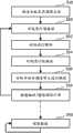
图7是描述了用于制造和操作非易失性存储系统的处理的流程图。在步骤548中,制造和配置非易失性存储系统以供使用。下面提供步骤548的更多细节。一旦制造和配置非易失性存储系统,该非易失性存储系统就可以用于对数据进行编程和读取。可选地进行步骤550作为对数据编程的处理的一部分。在一个示例实施方式中,对存储器单元进行预编程以甚至维持存储器单元上的磨损(步骤550)。在一个实施例中,存储器单元预编程到最高数据状态、随机模式或任何其他模式。在一些实施方式中,不需要进行预编程。FIG. 7 is a flowchart describing a process for manufacturing and operating a non-volatile memory system. In
在步骤552中,在编程前(以块或其他单位)擦除存储器单元。在一个实施例中,通过下述方式来擦除存储器单元:在足够的时间段内将p井提高到擦除电压(例如,20伏特),并且使被选择的块的字线接地,同时源极和位线浮置。在未被选择为要擦除的块中,字线浮置。由于电容式耦合的原因,未被选择的字线、位线、选择线和共同源极线也提高到擦除电压的相当大部分,从而阻止了对未被选择为要擦除的块的擦除。在被选择为要擦除的块中,将强电场施加到被选择的存储器单元的隧道氧化层,且被选择的存储器单元随着浮置栅极的电子发射到基板侧(通常通过福勒-诺得海姆(Fowler-Nordheim)隧穿机制)而被擦除。随着电子从浮置栅极转移到p井区域,被选择的单元的阈值电压降低。可以对整个存储器阵列、单个块或另一单位的存储器单元进行擦除。在一个实施例中,在对存储器单元进行擦除后,块中的所有经擦除的存储器单元将处于状态S0(下面所讨论)。擦除处理的一个实施方式包括将若干擦除脉冲施加到p井并且在擦除脉冲之间验证是否适当地擦除NAND串。In
在步骤554中,(可选地)进行软编程以使经擦除的存储器单元的擦除阈值电压的分布变窄。一些存储器单元可由于擦除处理而处于比必要的更深的擦除状态。软编程可以施加编程脉冲以将较深的擦除存储器单元的阈值电压移动到擦除阈值分布。In
在步骤556中,对块的存储器单元进行编程。可以响应于来自主机的编程请求或响应于内部处理来进行编程。在步骤558中,递增编程/擦除循环计数。非易失性存储系统将在寄存器、快闪存储器或其他位置中维持编程/擦除循环的计数。在每个编程/擦除循环后,递增编程/擦除循环计数。In
在编程后,可以读取块的存储器单元(步骤560)。在本领域中已知的许多不同的读取处理可以用于读取数据。在一些实施例中,读取处理包括使用ECC来校正错误。将读取的数据输出到请求读取操作的主机。可以由状态机、控制器或另一装置来进行ECC处理。After programming, the memory cells of the block can be read (step 560). Many different read processes known in the art can be used to read the data. In some embodiments, the read process includes using ECC to correct errors. Output the read data to the host requesting the read operation. ECC processing may be performed by a state machine, controller, or another device.
图7示出了擦除编程循环可以在不读取或独立于读取的情况下发生许多次(由步骤550至558组成的循环)、读取处理可以在不编程或独立于编程的情况下发生许多次,并且读取处理可以在编程后的任何时间发生(由步骤558与560之间的虚线表示)。可以按状态机的指示使用上述的各种电路进行图7的处理。在其他实施例中,可以按控制器的指示使用上述的各种电路进行图7的处理。Figure 7 shows that the erase-program loop can occur many times without or independently of reading (the loop consisting of
在成功编程处理(连同验证)结束时,视情况而定,存储器单元的阈值电压应该在经编程的存储器单元的一个或更多个阈值电压分布内或在经擦除的存储器单元的阈值电压分布内。图8示出了在每个存储器单元存储三位的数据时存储器单元阵列的示例阈值电压分布。然而,其他实施例可以对于每个存储器单元使用多于或少于三位的数据(例如,就如对于每个存储器单元三位的数据)。At the conclusion of a successful programming process (along with verify), the threshold voltages of the memory cells should be within one or more threshold voltage distributions of programmed memory cells or within the threshold voltage distribution of erased memory cells, as the case may be. Inside. 8 shows example threshold voltage distributions for a memory cell array when each memory cell stores three bits of data. However, other embodiments may use more or less than three bits of data per memory cell (eg, as in three bits of data per memory cell).
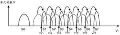
在图8的示例中,每个存储器单元存储三位的数据;因此,存在八个有效的阈值电压分布,也称为数据状态:S0、S1、S2、S3、S4、S5、S6和S7。在一个实施例中,数据状态S0低于0伏特且数据状态S1至S7高于0伏特。在其他实施例中,所有八个数据状态都高于0伏特,或者可以实施其他配置。在一个实施例中,S0的阈值电压分布比S1至S7的阈值电压分布宽。在一个实施例中,S0用于经擦除的存储器单元。从S0到S1至S7对数据进行编程。In the example of FIG. 8, each memory cell stores three bits of data; therefore, there are eight valid threshold voltage distributions, also referred to as data states: S0, S1, S2, S3, S4, S5, S6, and S7. In one embodiment, data state S0 is below 0 volts and data states S1 - S7 are above 0 volts. In other embodiments, all eight data states are above 0 volts, or other configurations may be implemented. In one embodiment, the threshold voltage distribution of S0 is wider than the threshold voltage distribution of S1 to S7. In one embodiment, SO is used for erased memory cells. Data is programmed from S0 to S1 to S7.
每个数据状态对应于存储在存储器单元中的三个数据位的唯一值。在一个实施例中,S0=111,S1=110,S2=101,S3=100,S4=011,S5=010,S6=001以及S7=000。也可以使用数据到状态S0至S7的其他映射。编程到存储器单元中的数据与单元的阈值电压水平之间的具体关系取决于针对单元采用的数据编码方案。例如,美国专利6,222,762和在2003年6月13日提交的美国专利申请公开2004/0255090“Tracking Cells For AMemory System”描述了用于多状态快闪存储器单元的各种数据编码方案,这两个专利文献的全部内容通过引用合并于此。在一个实施例中,使用格雷(Gray)码分配将数据值分配到阈值电压范围,以使得如果浮置栅极的阈值电压错误地偏移到其邻近的阈值电压分布,则仅影响一个位。然而,在其他实施例中,不使用格雷码。Each data state corresponds to a unique value for the three data bits stored in the memory cell. In one embodiment, S0=111, S1=110, S2=101, S3=100, S4=011, S5=010, S6=001 and S7=000. Other mappings of data to states S0 to S7 may also be used. The specific relationship between the data programmed into a memory cell and the cell's threshold voltage level depends on the data encoding scheme employed for the cell. For example, U.S. Patent 6,222,762 and U.S. Patent Application Publication 2004/0255090 "Tracking Cells For AMemory System," filed June 13, 2003, describe various data encoding schemes for multi-state flash memory cells, both of which The entire contents of this document are hereby incorporated by reference. In one embodiment, the data values are assigned to threshold voltage ranges using a Gray code assignment such that if the threshold voltage of a floating gate is incorrectly shifted to its neighboring threshold voltage distribution, only one bit is affected. However, in other embodiments, Gray codes are not used.
在一个实施例中,存储在存储器单元中的所有位的数据存储在同一逻辑页中。在其他实施例中,存储器单元中存储的每个位的数据对应于不同的逻辑页。因此,存储三位数据的存储器单元将会包括第一页中的数据、第二页中的数据和第三页中的数据。在一些实施例中,连接到同一字线的所有存储器单元将会将数据存储在相同的三个数据页中。在一些实施例中,连接到字线的存储器单元可以(例如,通过奇数位线和偶数位线或通过其他配置)分群组成不同的页组。In one embodiment, all bits of data stored in a memory cell are stored in the same logical page. In other embodiments, each bit of data stored in a memory cell corresponds to a different logical page. Thus, a memory cell storing three bits of data would include data in the first page, data in the second page, and data in the third page. In some embodiments, all memory cells connected to the same word line will store data in the same three data pages. In some embodiments, memory cells connected to word lines may be grouped (eg, by odd and even bit lines or by other configurations) into different page groups.
在一些装置中,将存储器单元擦除到状态S0。存储器单元可以从状态S0编程到状态S1至S7中的任一个状态。在一个实施例中,作为全序列编程而已知的是,存储器单元可以从擦除状态S0直接编程到编程状态S1至S7中的任一个状态。例如,要编程的全体存储器单元可以首先被擦除以使得全体中的所有存储器单元都处于擦除状态S0。在一些存储器单元正在从状态S0编程到状态S1时,其他存储器单元正在从状态S0编程到状态S2、从状态S0编程到状态S3、从状态S0编程到状态S4、从状态S0编程到状态S5、从状态S0编程到状态S6以及从状态S0编程到状态S7。由图8中的七个弯曲箭头图示性地描述了全序列编程。In some devices, memory cells are erased to state SO. Memory cells can be programmed from state S0 to any one of states S1-S7. In one embodiment, known as full sequence programming, memory cells can be programmed directly from erased state S0 to any of programmed states S1-S7. For example, a population of memory cells to be programmed may first be erased such that all memory cells in the population are in erased state SO. While some memory cells are being programmed from state S0 to state S1, other memory cells are being programmed from state S0 to state S2, from state S0 to state S3, from state S0 to state S4, from state S0 to state S5, Programming is from state S0 to state S6 and from state S0 to state S7. Full sequence programming is schematically depicted by the seven curved arrows in FIG. 8 .
图8示出了一组验证目标水平Vv1、Vv2、Vv3、Vv4、Vv5、Vv6和Vv7。这些验证水平用作为编程处理期间的比较水平。例如,在将存储器单元编程到状态S1时,系统将进行检查,以查看存储器单元的阈值电压是否达到了Vv1。如果存储器单元的阈值电压没有达到Vv1,则继续对该存储器单元进行编程,直到该存储器单元的阈值电压大于或等于Vv1为止。如果存储器单元的阈值电压达到了Vv1,则停止对该存储器单元进行编程。验证目标水平Vv2用于正被编程到状态S2的存储器单元。验证目标水平Vv3用于正被编程到状态S3的存储器单元。验证目标水平Vv4用于正被编程到状态S4的存储器单元。验证目标水平Vv5用于正被编程到状态S5的存储器单元。验证目标水平Vv6用于正被编程到状态S6的存储器单元。验证目标水平Vv7用于正被编程到状态S7的存储器单元。Figure 8 shows a set of verification target levels Vv1, Vv2, Vv3, Vv4, Vv5, Vv6 and Vv7. These verify levels are used as comparison levels during the programming process. For example, when programming a memory cell to state S1, the system will check to see if the threshold voltage of the memory cell has reached Vv1. If the threshold voltage of the memory cell does not reach Vv1, continue to program the memory cell until the threshold voltage of the memory cell is greater than or equal to Vv1. If the threshold voltage of the memory cell reaches Vv1, programming of the memory cell is stopped. The verify target level Vv2 is for the memory cells being programmed to state S2. Verify target level Vv3 is for memory cells being programmed to state S3. The verify target level Vv4 is for the memory cells being programmed to state S4. The verify target level Vv5 is for the memory cells being programmed to state S5. The verify target level Vv6 is for the memory cells being programmed to state S6. The verify target level Vv7 is for the memory cells being programmed to state S7.
图8还示出了一组读取比较水平Vr1、Vr2、Vr3、Vr4、Vr5、Vr6和Vr7。这些读取比较水平用作为读取处理期间的比较水平。通过测试存储器单元响应于分别施加到存储器单元的控制栅极的读取比较水平Vr1、Vr2、Vr3、Vr4、Vr5、Vr6和Vr7而接通还是保持断开,系统可以确定存储器单元针对哪些状态来存储数据。Figure 8 also shows a set of read comparison levels Vrl, Vr2, Vr3, Vr4, Vr5, Vr6 and Vr7. These read comparison levels are used as comparison levels during the read process. By testing whether a memory cell turns on or remains off in response to read compare levels Vr1 , Vr2 , Vr3 , Vr4 , Vr5 , Vr6 , and Vr7 respectively applied to the control gate of the memory cell, the system can determine for which states the memory cell is turned off. Storing data.
大体上,在验证操作和读取操作期间,被选择的字线连接到下述电压:针对每个读取操作(例如,参见图8中的读取比较水平Vr1、Vr2、Vr3、Vr4、Vr5、Vr6和Vr7)或验证操作(例如,参见图8中的验证目标水平Vv1、Vv2、Vv3、Vv4、Vv5、Vv6和Vv7)而指定该电压的水平,以确定相关存储器单元的阈值电压是否达到了此水平。在施加了字线电压后,测量存储器单元的传导电流以确定存储器单元是否响应于施加到字线的电压而接通。如果测量到传导电流大于一定值,则假定存储器单元接通且施加到字线的电压大于存储器单元的阈值电压。如果未测量到传导电流大于一定值,则假定存储器单元不接通且施加到字线的电压不大于存储器单元的阈值电压。在读取处理期间,未被选择的存储器单元在其控制栅极处被提供一个或更多个读取通过电压,以使得这些存储器单元将操作为通过栅极(例如,不管是否编程或擦除这些存储器单元,都对电流进行传导)。In general, during a verify operation and a read operation, the selected word line is connected to the following voltages: , Vr6, and Vr7) or a verify operation (see, for example, verify target levels Vv1, Vv2, Vv3, Vv4, Vv5, Vv6, and Vv7 in Figure 8) to specify the level of this voltage to determine whether the threshold voltage of the associated memory cell reaches this level. After the word line voltage is applied, the conduction current of the memory cell is measured to determine whether the memory cell turns on in response to the voltage applied to the word line. If the conduction current is measured to be greater than a certain value, it is assumed that the memory cell is on and the voltage applied to the word line is greater than the threshold voltage of the memory cell. If no conduction current greater than a certain value is measured, it is assumed that the memory cell is not turned on and the voltage applied to the word line is not greater than the threshold voltage of the memory cell. During the read process, unselected memory cells are provided with one or more read pass voltages at their control gates such that these memory cells will operate as pass gates (e.g., whether programmed or erased) These memory cells, all conduct current).
存在在读取或验证操作期间测量存储器单元的传导电流的许多方式。在一个示例中,存储器单元的传导电流是通过其使得感测放大器中的专用电容器放电或充电的速率来测量的。在另一示例中,被选择的存储器单元的传导电流允许(或无法允许)包括有该存储器单元的NAND串使对应的位线放电。在一段时间后测量位线上的电压以查看位线是否已放电。注意,本文所描述的技术可以与本领域中已知的用于验证/读取的不同方法一起使用。关于验证/读取的更多信息可以在以下专利文献中找到:(1)美国专利申请公开2004/0057287;(2)美国专利申请公开2004/0109357;(3)美国专利申请公开2005/0169082;以及(4)美国专利申请公开2006/0221692,其全部内容通过引用合并于此。根据本领域中已知的技术进行上述的读取和验证操作。因此,本领域普通技术人员可以改变许多所描述的细节。也可以使用本领域中已知的其他读取和验证技术。There are many ways of measuring the conduction current of a memory cell during a read or verify operation. In one example, the conduction current of a memory cell is measured by the rate at which it discharges or charges a dedicated capacitor in the sense amplifier. In another example, the conduction current of the selected memory cell allows (or does not allow) the NAND string including the memory cell to discharge the corresponding bit line. Measure the voltage on the bit line after a period of time to see if the bit line has discharged. Note that the techniques described herein can be used with different methods known in the art for verification/reading. More information on verification/reading can be found in the following patent documents: (1) US Patent Application Publication 2004/0057287; (2) US Patent Application Publication 2004/0109357; (3) US Patent Application Publication 2005/0169082; and (4) US Patent Application Publication 2006/0221692, the entire contents of which are hereby incorporated by reference. The read and verify operations described above are performed according to techniques known in the art. Accordingly, variations from many of the described details can be varied by one of ordinary skill in the art. Other reading and verification techniques known in the art can also be used.
在一些实施例中,施加到控制栅极的编程电压包括一系列脉冲,该一系列脉冲的量值随着每个连续的脉冲而增加预定步长(例如,0.2v、0.3v、0.4v或其他)。在脉冲之间,一些存储器系统验证各个存储器单元是否达到了它们的各自的目标阈值电压范围。例如,图9示出了施加到连接到共同字线的多个存储器单元的控制栅极的信号的一部分。图9示出了编程脉冲564、565及566,在编程脉冲之间具有一组验证脉冲。当在一个实施例中进行全序列编程时,编程脉冲之间的验证处理将针对阈值电压分布(数据状态)S1至S7中的每一个进行测试。因此,图9示出了具有对应于验证目标水平Vv1、Vv2、Vv3、Vv4、Vv5、Vv6和Vv7的量值的七个验证脉冲。在一些实施例中,可以跳过验证操作中的一个或更多个(并且因此,可以跳过验证脉冲中的一个或更多个),这是因为该验证操作是不必要的或是多余的。例如,如果正根据图8被编程的存储器单元均未达到Vv2,则没有理由以Vv7进行验证。关于跳过一个或更多个状态的验证的智能验证方案的更多信息可以在以下专利文献中找到:美国专利7,073,103、美国专利7,224,614、美国专利7,310,255、美国专利7,301,817、美国专利申请2001/0109362和美国专利申请2009/0147573,其全部内容通过引用合并于此。In some embodiments, the programming voltage applied to the control gate comprises a series of pulses whose magnitude increases with each successive pulse by a predetermined step size (eg, 0.2v, 0.3v, 0.4v, or other). Between pulses, some memory systems verify that individual memory cells have reached their respective target threshold voltage ranges. For example, FIG. 9 shows a portion of a signal applied to the control gates of a plurality of memory cells connected to a common word line. Figure 9 shows programming pulses 564, 565 and 566 with a set of verify pulses in between. When doing full sequence programming in one embodiment, the verify process between programming pulses will test each of the threshold voltage distributions (data states) S1-S7. Thus, FIG. 9 shows seven verify pulses having magnitudes corresponding to verify target levels Vv1 , Vv2 , Vv3 , Vv4 , Vv5 , Vv6 and Vv7 . In some embodiments, one or more of the verify operations (and thus, one or more of the verify pulses) may be skipped because the verify operations are unnecessary or redundant . For example, if none of the memory cells being programmed according to Figure 8 have reached Vv2, there is no reason to verify at Vv7. More information on smart verification schemes that skip verification of one or more states can be found in the following patent documents: US Patent 7,073,103, US Patent 7,224,614, US Patent 7,310,255, US Patent 7,301,817, US Patent Application 2001/0109362 and US Patent Application 2009/0147573, the entire contents of which are hereby incorporated by reference.
图8示出了包括一个阶段的编程处理,其中在该一个阶段期间对连接到同一字线的所有存储器单元同时进行编程。图10A至图10E示出了多阶段编程方法。在本实施例中,编程处理包括三个阶段。在编程前,擦除存储器单元以使得连接到共同字线的所有存储器单元处于擦除阈值电压分布E,如图10A所示。在编程的第一阶段期间,将(由于要存储在这些存储器单元中的数据而导致)目标是数据状态S4、S5、S6或S7的那些存储器单元编程到中间状态IM。一些存储器单元目标为数据状态S0、S1、S2或S3且保持处在擦除阈值电压分布E。由图10B图示性地描述了第一阶段。将编程到中间状态IM的存储器单元编程到目标阈值电压VvIM。Figure 8 shows a programming process that includes a phase during which all memory cells connected to the same word line are programmed simultaneously. 10A-10E illustrate a multi-stage programming method. In this embodiment, the programming process includes three stages. Prior to programming, memory cells are erased such that all memory cells connected to a common word line are at an erased threshold voltage distribution E, as shown in Figure 10A. During the first phase of programming, those memory cells targeted for data state S4, S5, S6 or S7 (due to the data to be stored in these memory cells) are programmed to an intermediate state IM. Some memory cells target data state S0, S1, S2 or S3 and remain at erased threshold voltage distribution E. The first stage is schematically depicted by Figure 10B. Memory cells programmed to intermediate state IM are programmed to target threshold voltage VvIM.
在图10A至图10E的编程处理的第二阶段期间,将处于擦除阈值电压分布E的那些存储器单元编程到其目标数据状态。例如,将要编程到数据状态S3的那些存储器单元从擦除阈值电压分布E编程到数据状态S3,将要编程到数据状态S2的那些存储器单元从擦除阈值电压分布E编程到数据状态S2,将要编程到数据状态S1的那些存储器单元从擦除阈值电压分布E编程到数据状态S1,并且在编程处理的第二阶段期间没有对处于数据状态S0的那些存储器单元进行编程。因此,擦除阈值电压分布E变成了数据状态S0。此外,在第二阶段期间,将存储器单元从中间状态IM编程到各个数据状态S4至S7。例如,将要编程到数据状态S7的那些存储器单元从中间状态IM编程到数据状态S7,将目标为处于数据状态S6的那些存储器单元从中间状态IM编程到数据状态S6,将要编程到数据状态S5的两个存储器单元从中间状态IM编程到数据状态S5,并且将要编程到数据状态S4的那些存储器单元从中间状态IM编程到数据状态S4。在图10C中示出了编程的该第二阶段。During the second phase of the programming process of FIGS. 10A-10E , those memory cells at erased threshold voltage distribution E are programmed to their target data states. For example, to program those memory cells to be programmed to data state S3 from erased threshold voltage distribution E to data state S3, to program those memory cells to be programmed to data state S2 from erased threshold voltage distribution E to data state S2, to program Those memory cells to data state S1 are programmed to data state S1 from the erased threshold voltage distribution E, and those memory cells in data state S0 are not programmed during the second phase of the programming process. Therefore, the erased threshold voltage distribution E becomes the data state S0. Furthermore, during the second phase, the memory cells are programmed from the intermediate state IM to the respective data states S4-S7. For example, those memory cells to be programmed to data state S7 are programmed from intermediate state IM to data state S7, those memory cells targeted to be in data state S6 are programmed from intermediate state IM to data state S6, those memory cells to be programmed to data state S5 are programmed to Two memory cells are programmed from intermediate state IM to data state S5, and those memory cells to be programmed to data state S4 are programmed from intermediate state IM to data state S4. This second stage of programming is shown in Figure 10C.
如在图10C中可见,在编程的第二阶段结束时,数据状态S1至S7与邻近的数据状态交叠。例如,数据状态S1与数据状态S2交叠,数据状态S2与数据状态S1和S3交叠,数据状态S3与数据状态S2和S4交叠,数据状态S4与数据状态S3和S5交叠,数据状态S5与数据状态S4和S6交叠,并且数据状态S6与数据状态S5和S7交叠。在一些实施例中,数据状态中的所有或一些数据状态并不交叠。As can be seen in FIG. 1OC, at the end of the second phase of programming, data states S1-S7 overlap adjacent data states. For example, data state S1 overlaps with data state S2, data state S2 overlaps with data states S1 and S3, data state S3 overlaps with data states S2 and S4, data state S4 overlaps with data states S3 and S5, and data state S5 overlaps data states S4 and S6, and data state S6 overlaps data states S5 and S7. In some embodiments, all or some of the data states do not overlap.
在编程的第三阶段中,数据状态S1至S7中的每一个状态变紧以使得其不再与邻近的状态交叠。由图10D图示性地对此进行了描述。在示出了数据状态S0至S7的步骤10E中描述了三个阶段的编程处理的最终结果。在一些实施例中,数据状态S0比数据状态S1至S7宽。In the third phase of programming, each of the data states S1 to S7 is compacted so that it no longer overlaps adjacent states. This is illustrated schematically by Figure 10D. The end result of the three-stage programming process is depicted in step 10E showing data states S0 to S7. In some embodiments, data state S0 is wider than data states S1-S7.
在一些实施例中,在第二阶段期间没有对要编程到数据状态S4的那些存储器单元进行编程,因此,这些存储器单元保持在中间状态IM。在第三编程阶段期间,将存储器单元从IM编程到S4。在其他实施例中,以其他状态为目标的存储器单元也可以在第二阶段期间保持在IM或E。In some embodiments, those memory cells to be programmed to data state S4 are not programmed during the second phase and therefore remain in intermediate state IM. During the third programming phase, memory cells are programmed from IM to S4. In other embodiments, memory cells targeting other states may also remain at IM or E during the second phase.
在一些编程处理中,可以并入粗糙的/精细的编程技术。例如,正被编程到目标状况(例如,Vv2)的存储器单元首先会被快速编程到与略低于目标状况的阈值电压状况相对应的粗糙状况(例如,比Vv2少了小量电压)。随后,存储器单元将会以更慢(且更精确)的方式编程到目标状况。该粗糙的/精细的编程技术可以用于编程到所有数据状态或数据状态的子集。In some programming processes, coarse/fine programming techniques may be incorporated. For example, a memory cell being programmed to a target condition (eg, Vv2) will first be rapidly programmed to a rough condition corresponding to a threshold voltage condition slightly below the target condition (eg, a small voltage less than Vv2). The memory cells will then be programmed to the target condition in a slower (and more precise) manner. This coarse/fine programming technique can be used to program to all data states or a subset of data states.
图11是描述了用于进行将连接到共同字线的存储器单元编程到一个或更多个目标(例如,数据状态或阈值电压范围)的处理的一个实施例的流程图。可以在图7的步骤556期间一次或多次进行图11的处理。例如,图11的处理可以用于将存储器单元从状态S0直接编程(例如,全序列编程)到状态S1至S7中的任一个状态。替选地,图11的处理可以用于进行图10A至图10E的处理的各阶段中的一个阶段或每个阶段。例如,在进行图10A的处理时,图11的处理用于实施包括将一些存储器单元从状态E编程到状态IM的第一阶段。然后,图11的处理可以再次用于实施包括将一些存储器单元从状态E编程到状态S1至S3以及从状态IM编程到状态S4至S7的第二阶段。图11的处理可以再次用于在第三阶段中调整状态S1至S7(参见图10D)。图11的处理也可以与其他多阶段编程处理一起使用。Figure 11 is a flowchart describing one embodiment of a process for performing programming of memory cells connected to a common word line to one or more targets (eg, data states or threshold voltage ranges). The process of FIG. 11 may occur one or more times during
通常,在编程操作期间施加到控制栅极的编程电压被施加为一系列编程脉冲。在编程脉冲之间的是用于进行验证的一组验证脉冲。在许多实施方式中,编程脉冲的量值随着每个连续的脉冲以预定步长增加。在图11的步骤570中,将编程电压(Vpgm)初始化至开始量值(例如,~12V至16V或另一合适的水平)并且将由状态机222所维持的编程计数器PC初始化为1。在步骤572中,将编程信号Vpgm的编程脉冲施加到被选择的字线(选择用于编程的字线)。在一个实施例中,正被编程的存储器单元的群组都连接到同一字线(被选择的字线)。未被选择的字线接收一个或更多个升压电压(例如,~9伏特)以进行在本领域中已知的升压方案。如果存储器单元应该进行编程,则对应的位线接地。另一方面,如果存储器单元应该保持在其当前阈值电压处,则对应的位线连接到Vdd以禁止编程。在步骤572中,将编程脉冲同时施加到连接到被选择的字线的所有存储器单元,以使得对连接到被选择的字线的所有存储器单元同时进行编程。即,同时(或在交叠的时间期间)对这些存储器单元进行编程。以此方式,除非这些存储器单元已被锁定于编程之外,否者连接到被选择的字线的所有存储器单元将同时改变其阈值电压。Typically, the programming voltage applied to the control gate during a programming operation is applied as a series of programming pulses. Between the programming pulses is a set of verify pulses for verifying. In many implementations, the magnitude of the programming pulse increases with each successive pulse by a predetermined step size. In
在步骤574中,使用一组适当的目标水平来验证适当的存储器单元以进行一个或更多个验证操作。在一个实施例中,通过将适当的验证比较电压(Vv1、Vv2、Vv3、Vv4、Vv5、Vv6和Vv7)施加到被选择的字线并且将当前读取通过电压施加到未被选择的字线来进行验证处理。下面提供了关于确定当前读取通过电压的更多细节。In
在步骤576中,确定是否所有存储器单元都达到了其目标阈值电压。如果所有存储器单元都达到了其目标阈值电压,则编程处理完成且是成功的,这是因为所有被选择的存储器单元都被编程到其目标状态并且被验证为其目标状态。在步骤578中报告了“通过”(PASS)状态。如果在步骤576中确定不是所有存储器单元都达到了其目标阈值电压,则编程处理继续到步骤580。In
在步骤580中,系统对还没有达到其各自的目标阈值电压分布的存储器单元的数目进行计数。即,系统对验证处理失败的单元的数目进行计数。该计数可以由状态机、控制器或其他逻辑来完成。在一个实施方式中,感测块300中的每一个(参见图3)将存储其各自的单元的状态(通过/失败)。可以使用数字计数器对这些值进行计数。如上所述,感测块中的许多感测块具有线或在一起的输出信号。因此,检查一条线就可以指示出大群组的单元中没有单元验证失败。通过适当地组织线或在一起的线(例如,类二叉树结构),二进制搜索方法可以用于确定失败的单元的数目。在这样的方式中,如果少量单元失败,则快速地完成计数。如果大量单元失败,则计数花费较长的时间。可以在美国专利申请公开2008/0126676中找到更多的信息,该申请的全部内容通过引用合并于此。在另一替选方式中,每一个感测放大器可以在其对应的存储器单元失败的情况下输出模拟电压或电流,并且模拟电压或电流求和电路可以用于对失败的存储器单元的数目进行计数。In
在一个实施例中,存在一个总计数,该总计数反映了最后的验证步骤失败的当前正被编程的存储器单元的总数目。在另一实施例中,针对每个数据状态保持分别计数。In one embodiment, there is a total count that reflects the total number of memory cells currently being programmed that failed the last verify step. In another embodiment, separate counts are maintained for each data state.
在步骤582中,确定来自步骤580的计数是否小于或等于预定限制。在一个实施例中,预定限制是在读取处理期间对于存储器单元的页可由ECC校正的位的数目。如果失败的单元的数目小于或等于预定限制,则编程处理可以停止,且在步骤578中报告“通过”状态。在此情况下,足够的存储器单元被正确地编程,使得可以在读取处理期间使用ECC来校正未完全编程的少数剩余的存储器单元。在一些实施例中,步骤580将针对每个扇区、每个目标数据状态或其他单位来对失败的单元的数目进行计数,且在步骤582中这些计数将单独地或共同地与阈值进行比较。In
在另一实施例中,预定限制可以小于在读取处理期间可由ECC校正的位的数目,以允许未来的错误。当对页的少于所有存储器单元的存储器单元进行编程或对于仅一个数据状态(或少于所有状态)的计数进行比较时,预定限制可以是在读取处理期间对于存储器单元的页可由ECC校正的位的数目的一部分(按比例或不按比例)。在一些实施例中,限制不是预定的。相反,该限制基于已对于页计数的错误的数目、进行的编程擦除循环的次数、温度或其他标准而变化。In another embodiment, the predetermined limit may be less than the number of bits correctable by ECC during the read process to allow for future errors. When programming less than all memory cells of a page or comparing counts for only one data state (or less than all states), the predetermined limit may be correctable by ECC for a page of memory cells during a read process The fraction (proportional or not) of the number of bits. In some embodiments, the limit is not predetermined. Instead, the limit varies based on the number of errors that have been counted for the page, the number of program-erase cycles performed, temperature, or other criteria.
如果失败的存储器单元的数目不小于预定限制,则编程处理在步骤584处继续且相对于编程限制值(PL)对编程计数器PC进行检查。编程限制值的一个示例是20;然而,可以使用其他值。如果编程计数器PC不小于编程限制值PL,则编程处理被认为已失败并在步骤588中报告失败状态。如果编程计数器PC小于编程限制值PL,则该处理在步骤586处继续,在此时间期间编程计数器PC递增1且编程电压Vpgm步进直至下一量值。例如,下一脉冲的量值将比先前脉冲大一个步长(例如,0.1伏特至0.4伏特的步长)。在步骤586后,该处理循环回到步骤572并将另一编程脉冲施加到被选择的字线。If the number of failed memory cells is not less than the predetermined limit, the programming process continues at
图12是描述了用于从非易失性存储器进行读取的处理的一个实施例的流程图。在图12中所描述的处理是图7的步骤560的一个示例实施方式。图12的处理(除步骤640外)也可以用于在编程期间进行验证。在图12的步骤640中,接收读取数据的请求。可以从主机或其他实体接收该请求。在一些实施例中,可以在没有来自主机的请求的情况下进行读取处理。在步骤642中,控制器244将获得所进行的编程/擦除循环的次数的表示。如上所示,该编程/擦除循环的表示可以存储在寄存器、快闪存储器或其他存储位置中。在一个实施例中,经历过零次编程/擦除循环的存储器系统完全是新的,而经历过100次编程/擦除循环的存储器系统被视为处于循环状况。也可以使用其他值。Figure 12 is a flowchart describing one embodiment of a process for reading from non-volatile memory. The process depicted in FIG. 12 is one example implementation of
在步骤644中,控制器244将获得针对循环存储器而优化的读取通过电压(下面称为Vread0)。在步骤646中,控制器244将获得针对新存储器而优化的开始读取通过电压(下面称为Vread1)。在步骤648中,控制器244将基于针对循环存储器而优化的读取通过电压(Vread0)、针对新存储器而优化的读取通过电压(Vread1)及所进行的编程/擦除循环的表示来动态计算当前读取通过电压(Vreadc)以用于当前读取(或验证)操作。存在可以用于确定当前读取通过电压(Vreadc)的许多不同函数。下面讨论一些实施例的更多细节。In
在步骤650中,系统将把读取比较电压(Vcgr)施加到被选择的字线(WLn)。回看图8,Vcgr的示例包括Vr1、Vr2、Vr3、Vr4、Vr5、Vr6和Vr7。如果正在进行验证处理,则比较电压将是Vv1、Vv2、Vv3、Vv4、Vv5、Vv6和Vv7。在步骤652中,系统将把在步骤648中所确定的当前读取通过电压(Vreadc)施加到未被选择的字线,但邻近的字线(WLn+1和WLn-1)除外。在步骤654中,将另一读取通过电压(VreadK)施加到邻近的字线(WLn+1和WLn-1)。在步骤656中,系统将如上文所讨论的那样,对连接到被选择的字线WLn的一个或更多个被选择的存储器单元的状况进行感测。In
可以针对多个读取比较值多次进行步骤650至656,以确定一个或更多个存储器单元以多个状态中的哪个状态来保存数据。在步骤658中,基于各种感测(步骤650至656的重复),系统将确定被存储在每一个被选择的存储器单元中的数据值。在步骤660中,报告该数据(例如,报告给主机)。注意,在上面的讨论中,假定由控制器获得针对循环存储器而优化的读取通过电压(Vread0)、针对新存储器而优化的读取通过电压(Vread1)、以及所进行的编程/擦除循环的表示,以动态地自动计算(或调整)当前读取通过电压(Vreadc)。在一些实施例中,其他组件也可以计算当前读取通过电压(例如,状态机或其他组件)。
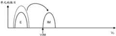
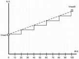
针对循环存储器而优化的读取通过电压(Vread0)是比针对新存储器而优化的读取通过电压(Vread1)高的读取通过电压,以补偿编程噪声和数据留存问题。针对新存储器而优化的读取通过电压(Vread1)是经优化以减少读取干扰的影响的、较低的通过电压。图13是描述了Vread1与Vread0的关系的图表。垂直轴是电压且水平轴是循环。在一个实施例中,假定在首次操作系统(零次循环)时要使用的最佳的读取通过电压是Vread1。在100次循环后,通过将Vread0用作为当前读取通过电压而优化该系统。图12的步骤648包括基于Vread0、Vread1以及所进行的编程/擦除循环的次数的表示而动态地自动计算当前读取通过电压。存在可以用于计算当前读取通过电压的许多不同的函数。在一个实施例中,使用已知的数学运算(例如,y=mx+b)而将线从Vread1模型化到Vread0。通过知道存储器处于哪个循环,可以沿着该线计算适当的电压。这样的线在图13中描述为将Vread1直接连接到Vread0的虚线。The read pass voltage optimized for cycled memory (Vread0) is a higher read pass voltage than the read pass voltage optimized for fresh memory (Vread1) to compensate for programming noise and data retention issues. The read pass voltage optimized for the new memory (Vread1 ) is a lower pass voltage optimized to reduce the effect of read disturb. FIG. 13 is a graph describing the relationship between Vread1 and Vread0. The vertical axis is voltage and the horizontal axis is cycle. In one embodiment, it is assumed that the optimal read pass voltage to use when first operating the system (zero cycles) is Vread1. After 100 cycles, the system is optimized by using VreadO as the current read pass voltage. Step 648 of FIG. 12 includes dynamically and automatically calculating the current read pass voltage based on Vread0, Vread1 and an indication of the number of program/erase cycles performed. There are many different functions that can be used to calculate the current read pass voltage. In one embodiment, the line is modeled from Vread1 to Vread0 using known mathematical operations (eg, y=mx+b). By knowing which cycle the memory is in, the appropriate voltage can be calculated along that line. Such a line is depicted in FIG. 13 as a dashed line connecting Vread1 directly to Vread0.
用于计算当前读取通过电压的另一实施例使用步进函数,以使得每20次循环,当前读取通过电压就增加Vread1与Vread0之间的距离的五分之一。因此,如果Vread0比Vread1高两伏特,则在20次循环后当前读取通过电压增加了0.4伏特,在40次循环后当前读取通过电压又增加0.4伏特等,如此直到将当前读取通过电压设置成等于Vread0的100次循环为止。图13图示性地以实线描述了该步进函数。Another embodiment for calculating the current read pass voltage uses a step function such that every 20 cycles the current read pass voltage increases by one-fifth of the distance between Vread1 and Vread0. So if Vread0 is two volts higher than Vread1, the current read pass voltage increases by 0.4 volts after 20 cycles, another 0.4 volts after 40 cycles, etc., until the current read pass voltage is increased by 0.4 volts Set to be equal to 100 cycles of Vread0. Figure 13 graphically depicts this step function with solid lines.
用于计算当前读取通过电压的另一实施例是控制器基于0与100之间的循环次数而在Vread0与Vread1之间进行内插。在100次循环后,控制器将对于当前读取通过电压始终使用Vread0。也可以使用用于确定当前读取通过电压的其他函数。Another embodiment for calculating the current read pass voltage is for the controller to interpolate between Vread0 and Vread1 based on the number of cycles between 0 and 100. After 100 cycles, the controller will always use VreadO for the current read pass voltage. Other functions for determining the current read pass voltage can also be used.
在一些实施例中,存储器系统将包括一个存储器管芯和一个控制器。在其他实施例中,存储器系统可以包括连接到共同控制器的多个存储器管芯。图14是示出了具有连接到多个存储器管芯(管芯A和管芯B)的单个控制器的存储器系统的一个示例的框图。在这样的实施例中,系统可以对于每个管芯分别记录编程/擦除循环的次数,并将这些次数存储在快闪存储器中的合适的管芯上。替选地,编程/擦除循环计数可以存储在控制器上。In some embodiments, a memory system will include a memory die and a controller. In other embodiments, a memory system may include multiple memory dies connected to a common controller. 14 is a block diagram illustrating one example of a memory system with a single controller connected to multiple memory dies (Die A and Die B). In such an embodiment, the system may record the number of program/erase cycles separately for each die and store the number on the appropriate die in flash memory. Alternatively, the program/erase cycle count can be stored on the controller.
图14示出了存储其自身的编程/擦除循环计数的各个管芯(管芯A的P/E_A和管芯B的P/E_B)。每个管芯存储其自身的针对新存储器而优化的开始读取通过电压(Vread1)。即,管芯A将存储Vread1_A且管芯B将存储其自身的Vread1_B。替选地,这些开始读取通过电压(Vread1_A和Vread1_B)可以存储在控制器上或系统中的其他位置。取决于实施方式和制造处理,Vread1_A和Vread1_B可以是相同的电压或不同的电压。在存储器系统中具有多个管芯时,图12中的步骤642将包括针对适当的管芯获得适当的所进行的编程/擦除循环的表示,且步骤646将包括针对适当的管芯获得适当的针对新存储器而优化的开始读取通过电压(Vread1)。在读取处理器将需要从多个管芯读取数据的系统中,于是步骤12将包括对于每个管芯分别进行步骤642至658。在一个实施例中,多个管芯将共享相同的针对循环存储器而优化的读取通过电压(Vread0)。在其他实施例中,多个管芯将具有不同的针对循环存储器而优化的读取通过电压(Vread0)。Figure 14 shows each die storing its own program/erase cycle count (P/E_A for Die A and P/E_B for Die B). Each die stores its own start read pass voltage (Vread1 ) optimized for new memory. That is, Die A will store Vread1_A and Die B will store its own Vread1_B. Alternatively, these start read pass voltages (Vread1_A and Vread1_B) may be stored on the controller or elsewhere in the system. Depending on the implementation and manufacturing process, Vread1_A and Vread1_B may be the same voltage or different voltages. When there are multiple dies in the memory system,
回看图12,步骤650至656包括设置适当的电压并且感测被选择的存储器单元的状况。图15描述了接收由步骤650至654所施加的适当的电压的三个NAND串的一部分。在一些实施例中,同时进行步骤650至654。如在图15中可见,被选择的字线(WLn)接收读取比较电压Vcgr。邻近的字线WLn+1和WLn-1接收VreadK。所有其他未被选择的字线将接收(在图12的步骤648中所计算的)当前读取通过电压Vreadc。Referring back to Figure 12,
在一些实施例中,VreadK比VreadC略高(例如,高0伏特至1伏特)。在其他实施例中,VreadK可以与VreadC相同。在另外的其他实施例中,VreadK可以基于WLn在NAND串中的位置、正被写入的数据、所进行的编程/擦除循环的次数、邻近的字线中的数据或其他方案而变化。使用邻近的字线上的读取通过电压的示例可以在美国专利7,898,864和美国专利7,499,319中找到,该两个专利的全部内容通过引用合并于此。In some embodiments, VreadK is slightly higher (eg, 0-1 volt higher) than VreadC. In other embodiments, VreadK may be the same as VreadC. In yet other embodiments, VreadK may vary based on the location of WLn in the NAND string, the data being written, the number of program/erase cycles performed, data in adjacent word lines, or other schemes. Examples of using read pass voltages on adjacent word lines can be found in US Patent 7,898,864 and US Patent 7,499,319, the entire contents of which are hereby incorporated by reference.
图16是描述了用于制造和配置非易失性存储器系统的处理的一个实施例的流程图。在图16中所描述的处理是图7中的步骤548的一个示例实施方式。在图16的步骤740中,使用在本领域中已知的技术来设计存储器系统。在步骤742中,确定针对循环存储器而优化的读取通过电压(Vread0)。可以使用模拟、试验或测试来进行步骤742。下面将提供步骤742的更多细节。在步骤744中,制造存储器系统。期望可以制造存储器系统的数百个、数千个或数百万个副本。本文所描述的技术不要求任何特定的制造处理并且可以使用已知的制造处理。在步骤746中,对于晶片的不同管芯(和/或不同的块)分别确定针对新存储器而优化的读取通过电压(Vread1)。可以使用模拟、测试或实验来进行在步骤746中所进行的处理。在一个实施例中,在作为管芯分类(die sort)处理的一部分的制造处理期间进行步骤746的处理。下面提供关于步骤746的更多细节。在步骤748中,存储器系统将被配置成对所进行的编程/擦除循环的次数进行监视和计数。例如,将提供一个或更多个存储器位置或寄存器以存储对所进行的编程/擦除循环的次数的计数或对该次数的其他表示。代码可以安装在控制器的存储器中以记录编程/擦除循环。替选地,可以添加专用硬件以对所进行的编程/擦除循环的次数进行计数。在步骤750中,存储器系统被配置成基于针对循环存储器而优化的读取通过电压(Vread0)、针对新存储器而优化的读取通过电压(Vread1)、以及所进行的编程/擦除循环的次数而动态地自动计算当前读取通过电压(Vreadc)。例如,控制器可以加载有软件以实施上面关于图13所描述的任何功能并且进行图12中的处理的全部或一部分。Figure 16 is a flowchart describing one embodiment of a process for fabricating and configuring a non-volatile memory system. The process depicted in FIG. 16 is one example implementation of
图17是描述了用于确定针对循环存储器而优化的读取通过电压(Vread0)的处理的一个实施例的流程图。图17中所描述的处理是进行图16中的步骤742的一个示例实施方式。另外,可以对样本部分进行图17中的处理,或可以使用模拟或其他类型的实验来进行图17中的处理。在图17的步骤802中,存储器系统循环了X次。循环的次数可以基于特定实施方式而变化。在一个实施例中,步骤802将包括使存储器系统循环100次以使得存储器系统现在处于循环状况下。在步骤804中,将为读取通过电压设置初始值。在一个实施例中,初始值是10伏特。在步骤806中,测试数据将被编程到存储器中。在步骤808中,系统将确定失败位(FB)的数目。失败位(FB)的数目是在编程处理结束时没有被编程到适当的数据状态的存储器单元的数目。例如,回看图11中的处理,如果失败位的数目小于预定限制(参见步骤582)或者编程的重复的次数达到了限制(参见步骤584),则存储器系统将停止编程。在任一情况下,在编程处理结束时,一些存储器单元没有被适当地编程。步骤808包括对没有适当地编程的存储器单元的数目进行计数。在步骤806和808的多次重复后,系统将具有多个失败位(FB)值,可以在图表中绘制这些失败位(FB)值,并且可以针对这些失败位(FB)值将曲线拟合于数据。在步骤810中,确定曲线是否已变平。如果曲线没有变平,则在步骤812中改变读取通过电压。例如,可以将读取通过电压降低0.2伏特(或某个其他值)。在步骤812中降低读取通过电压后,处理循环回到步骤806,并进行步骤806至808的另一重复。随着步骤806和808的每次重复,确定新的失败位值(FB)。在拟合所有FB数据的曲线开始变平时,假定改变读取通过电压将不再对性能具有显著的影响。因此,在失败位曲线已经变平(参见步骤810)时,处理将在步骤814处继续,并将把步骤806至808的最后一次重复的当前读取通过电压存储为针对循环存储器而优化的读取通过电压(Vread0)。Figure 17 is a flowchart describing one embodiment of a process for determining a read pass voltage (VreadO) optimized for cycling memory. The process depicted in FIG. 17 is one example implementation of performing
虽然图17提供了用于确定针对循环存储器而优化的读取通过电压的一个示例实施方式,但也可以使用其他处理。在一个实施例中,将针对晶片进行图17,使得晶片上的所有管芯将具有相同的针对循环存储器而优化的读取通过电压(Vread0)。在一些实施例中,对于与当前设计相关联的所有晶片,可以一次针对多个晶片计算针对循环存储器而优化的读取通过电压(Vread0)。例如,可以针对为特定设计而制造的所有晶片来计算针对循环存储器而优化的读取通过电压(Vread0)。While FIG. 17 provides one example implementation for determining a read pass voltage optimized for cycling memory, other processes may be used. In one embodiment, Figure 17 will be performed for a wafer such that all dies on the wafer will have the same read pass voltage (Vread0) optimized for cycle memory. In some embodiments, the read pass voltage optimized for cycling memory (VreadO) can be calculated for multiple dies at a time for all dies associated with the current design. For example, a read pass voltage optimized for cycling memory (Vread0) can be calculated for all wafers manufactured for a particular design.
图18是描述了用于确定针对新存储器而优化的读取通过电压(Vread1)的处理的实施例的流程图。图18中的处理是图16中的步骤746的一个示例实施方式。在一个示例中,图18中的处理是作为制造期间的测试阶段的一部分而进行的,其与管芯分类处理一致(或作为管芯分类处理的一部分)。在一个示例实施方式中,系统将针对晶片上的每个管芯来分别计算针对新存储器而优化的读取通过电压(Vread1)。替选地,系统可以针对晶片上的每个管芯的每个块来确定针对新存储器而优化的读取通过电压(Vread1)。Figure 18 is a flowchart describing an embodiment of a process for determining a read pass voltage (Vread1) optimized for a new memory. The process in FIG. 18 is an example implementation of
在图18的步骤902中,系统(例如,测试设备)将使用针对循环存储器而优化的读取通过电压(Vread0)来对晶片上的所有管芯进行编程。步骤902可以包括对随机测试模式或预定测试模式进行编程。在步骤904中,系统将确定晶片的成品率。即,系统将确定每个管芯有多少个失败位。如果失败位的数目小于预定数目,则该管芯被视为可接受的。如果失败位的数目高于预定数目,则拒绝该管芯。可以通过在本领域中已知的处理来进行晶片的成品率的确定(管芯分类的一部分)。在一组实施例中,晶片的成品率的确定是基于使用针对循环存储器而优化的读取通过电压(Vread0),而不使用针对新存储器而优化的读取通过电压(Vread1)。In step 902 of Figure 18, the system (eg, test equipment) will program all the die on the wafer using a read pass voltage (Vread0) optimized for cycle memory. Step 902 may include programming a random test pattern or a predetermined test pattern. In step 904, the system will determine the yield of the wafer. That is, the system will determine how many failed bits per die. If the number of failed bits is less than a predetermined number, the die is considered acceptable. If the number of failed bits is higher than a predetermined number, the die is rejected. The determination of the yield of the wafer (part of die sorting) can be done by processes known in the art. In one set of embodiments, the yield of the wafer is determined based on using a read pass voltage optimized for cycled memory (Vread0) instead of a read pass voltage optimized for new memory (Vread1).
如上所述,一个实施例包括针对每个管芯确定单独的针对新存储器而优化的读取通过电压(Vread1)。因此,在步骤906中,选择晶片上的一个管芯。假定步骤906将仅选择在步骤904中由于成功制造而被接受的管芯。在步骤908中,将使用针对循环存储器而优化的读取通过电压(Vread0)来编程该选定的管芯。在步骤910中,系统将基于步骤908中的编程来确定失败位的数目。在步骤912中,当前用于编程选定的管芯的读取通过电压将被降低预定步长(例如,0.2伏特或0.4伏特或另一数目)。在步骤914中,再次编程管芯,但这次使用(如在步骤912中降低的)较低的读取通过电压。在步骤916中,系统将根据最后一次编程(步骤914的最后重复)来确定失败位的数目。在步骤918中,确定编程的最后一次重复中的失败位的数目(FBx)是否小于在使用针对循环存储器而优化的读取通过电压(Vread0)时的失败位的数目的预定百分比。在一个示例中,预定百分比是150%,使得步骤918来测试编程的最后一次重复中的失败位的数目(FBx)是否小于在使用针对循环存储器而优化的读取通过电压时发生的失败位的数目的1.5倍。虽然步骤918的一个示例使用了1.5,但也可以使用其他数目(或百分比)。只要编程的当前重复的失败位的数目小于与使用针对循环存储器而优化的读取通过电压相关联的失败位的预定百分比(例如,150%或1.5),就将重复步骤912至918的循环。一旦失败位的数目多于因使用针对循环存储器而优化的读取通过电压而获得的失败位的数目的1.5倍,则循环将停止,并且在步骤920中存储下述读取通过电压作为当前管芯的针对新存储器而优化的读取通过电压(Vread1):其是失败位的数目(FBx)小于使用针对循环存储器而优化的读取通过电压的失败位的数目的1.5倍的最后的读取通过电压。在步骤922中,确定是否存在要操作的更多管芯。如果存在还没有被测试的更多的管芯,则处理循环到步骤906并选择下一个管芯。如果对于特定晶片不存在要操作的更多管芯,则处理完成(步骤924)。在一个实施例中,系统可以对多个管芯并行地操作而不是对管芯顺序地操作。在一些实施例中,(在编程期间)Vread0和Vread1用于读取和验证两者。As described above, one embodiment includes determining a separate read pass voltage (Vread1 ) optimized for new memory for each die. Therefore, in step 906, one die on the wafer is selected. It is assumed that step 906 will only select dies that were accepted due to successful fabrication in step 904 . In step 908, the selected die will be programmed with a read pass voltage (Vread0) optimized for cycle memory. In step 910 the system will determine the number of failed bits based on the programming in step 908 . In step 912, the read pass voltage currently used to program the selected die will be lowered by a predetermined step size (eg, 0.2 volts or 0.4 volts or another number). In step 914, the die is programmed again, but this time using a lower read pass voltage (as lowered in step 912). In step 916, the system will determine the number of failed bits from the last programming (last iteration of step 914). In step 918, it is determined whether the number of failed bits (FBx) in the last iteration of programming is less than a predetermined percentage of the number of failed bits when using a read pass voltage (Vread0) optimized for cycle memory. In one example, the predetermined percentage is 150%, so that step 918 tests whether the number of failed bits (FBx) in the last iteration of programming is less than the number of failed bits that would occur when using a read pass voltage optimized for cycle memory 1.5 times the number. While one example of step 918 uses 1.5, other numbers (or percentages) may be used. The loop of steps 912 to 918 will repeat as long as the number of failed bits programmed for the current iteration is less than a predetermined percentage (eg, 150% or 1.5) of failed bits associated with using a read pass voltage optimized for cycling the memory. Once the number of failed bits is more than 1.5 times the number of failed bits obtained by using a read pass voltage optimized for cycling the memory, the loop will stop and the following read pass voltage will be stored in step 920 as the current tube Core's read pass voltage optimized for new memory (Vread1): which is the last read where the number of failed bits (FBx) was less than 1.5 times the number of failed bits using the read pass voltage optimized for cycled memory through voltage. In step 922, it is determined whether there are more die to operate. If there are more dies that have not been tested, then processing loops to step 906 and the next die is selected. If there are no more die to operate on for the particular wafer, then the process is complete (step 924). In one embodiment, the system may operate on multiple dies in parallel rather than sequentially. In some embodiments, (during programming) Vread0 and Vread1 are used for both reading and verifying.
在一个替选方式中,可以对样本存储器或一个代表性存储器而不是单独的管芯进行图18中的处理。以此方式,晶片的所有管芯将具有相同的Vread1,并且用于计算Vreadc的功能可以构建到控制器中。在其他实施例中,可以使用模拟来进行图18中的处理。In an alternative, the processing in Figure 18 may be performed on sample memory or a representative memory rather than individual dies. In this way, all dies of a wafer will have the same Vread1 and the functionality for calculating Vreadc can be built into the controller. In other embodiments, simulations may be used to perform the process in FIG. 18 .
一个实施例包括:获得编程/擦除循环的表示;基于编程/擦除擦除循环的表示来动态确定被选择的字线的同一侧上的多条字线的当前读取通过电压;以及从连接到被选择的字线的一个或更多个非易失性存储元件读取数据。读取数据包括将所确定的当前读取通过电压施加到被选择的字线的同一侧上的多条字线、以及将读取电压施加到被选择的字线。One embodiment includes: obtaining a representation of the program/erase cycle; dynamically determining the current read pass voltages for multiple word lines on the same side of the selected word line based on the representation of the program/erase cycle; One or more non-volatile storage elements connected to the selected word line read data. Reading data includes applying the determined current read pass voltage to a plurality of word lines on the same side of the selected word line, and applying the read voltage to the selected word line.
一个实施例包括:多个非易失性存储元件;与非易失性存储元件通信的多条字线和位线;以及与非易失性存储元件通信以对非易失性存储元件进行编程、擦除和读取的一个或更多个管理电路。一个或更多个管理电路通过以下方式从非易失性存储元件进行读取:获得编程/擦除循环的表示;针对被选择的字线的同一侧上的多条字线,基于编程/擦除擦除循环的表示来动态确定当前读取通过电压;以及通过将所确定的当前读取通过电压施加到被选择的字线的同一侧上的多条字线并将读取电压施加到被选择的字线来从连接到被选择的字线的一个或更多个非易失性存储元件读取数据。One embodiment includes: a plurality of nonvolatile storage elements; a plurality of word lines and bit lines in communication with the nonvolatile storage elements; and in communication with the nonvolatile storage elements to program the nonvolatile storage elements , erase and read one or more management circuits. One or more supervisory circuits read from non-volatile storage elements by: obtaining a representation of a program/erase cycle; for multiple word lines on the same side of the selected word line, based on Dynamically determining a current read pass voltage through a representation of an erase cycle; and by applying the determined current read pass voltage to a plurality of word lines on the same side of the selected word line and applying the read voltage to the selected word line A word line is selected to read data from one or more non-volatile storage elements connected to the selected word line.
一个实施例包括:获得第一读取通过电压;读取开始读取通过电压,该开始读取通过电压是特定于第一管芯而计算的,以导致新状况下的第一管芯的失败位的数目处于由第一读取通过电压所导致的、新状况下的第一管芯的失败位的数目的预定百分比内;获得第一管芯的编程/擦除循环的表示;基于第一读取通过电压、开始读取通过电压及第一管芯的编程/擦除擦除循环的表示来动态确定第一当前读取通过电压;以及使用第一当前读取通过电压从第一管芯读取数据。One embodiment includes: obtaining a first read pass voltage; reading a start read pass voltage calculated specific to the first die to cause failure of the first die in a new condition the number of bits is within a predetermined percentage of the number of failed bits of the first die under new conditions caused by the first read pass voltage; obtaining a representation of the program/erase cycles of the first die; based on the first dynamically determining a first current read pass voltage using the first current read pass voltage, starting the read pass voltage, and a representation of a program/erase erase cycle of the first die; and using the first current read pass voltage from the first die read data.
一个实施例包括:布置在第一管芯和第二管芯上的多个非易失性存储元件;以及与第一管芯和第二管芯通信以对第一管芯和第二管芯上的非易失性存储元件进行编程、擦除和读取的一个或更多个管理电路。一个或更多个管理电路通过以下方式从第一管芯上的非易失性存储元件进行读取:获得第一读取通过电压;读取开始读取通过电压,该开始读取通过电压是特定于第一管芯而计算的,以导致新状况下的第一管芯的失败位的数目处于由用于新状况下的第一管芯的第一读取通过电压所导致的失败位的数目的预定百分比内;获得第一管芯的编程/擦除循环的表示;基于第一读取通过电压、开始读取通过电压及第一管芯的编程/擦除擦除循环的表示来动态确定第一当前读取通过电压;以及使用第一当前读取通过电压从第一管芯读取数据。One embodiment includes: a plurality of non-volatile storage elements disposed on the first die and the second die; and communicating with the first die and the second die to One or more management circuits for programming, erasing and reading non-volatile storage elements on the device. The one or more managing circuits read from the non-volatile storage element on the first die by: obtaining a first read pass voltage; reading a start read pass voltage, the start read pass voltage being Calculated specific to the first die such that the number of failed bits resulting in the first die in the new condition is within the number of failed bits caused by the first read pass voltage for the first die in the new condition within a predetermined percentage of the number; obtain a representation of the first die's program/erase cycle; dynamically Determining a first current read pass voltage; and reading data from the first die using the first current read pass voltage.
一个实施例包括:确定循环存储器的第一读取通过电压;分别确定一个或更多个管芯的一个或更多个开始读取通过电压,并将相应的开始读取通过电压存储到相应管芯上;配置各自均包括一个或更多个管芯的非易失性存储装置以监视管芯的编程/擦除循环;以及配置各自均包括一个或更多个管芯的非易失性存储装置以从管芯读取数据并基于循环存储器的第一读取通过电压、相应的开始读取通过电压及编程/擦除循环计数来动态调整用于读取数据的当前读取通过电压。One embodiment includes: determining a first read pass voltage for the cycle memory; determining one or more start read pass voltages for one or more dies, respectively, and storing the corresponding start read pass voltages to the corresponding dies on-die; configuring non-volatile storage devices each comprising one or more dies to monitor program/erase cycles of the dies; and configuring non-volatile storage devices each comprising one or more dies The device reads data from the die and dynamically adjusts the current read pass voltage for reading data based on the first read pass voltage cycling the memory, the corresponding starting read pass voltage, and the program/erase cycle count.
一个实施例包括:使用模拟来确定循环存储器的第一读取通过电压;通过识别下述通过电压来确定管芯的开始读取通过电压,该通过电压导致新状况下的管芯的失败位的数目处于通过使用第一读取通过电压所导致的、新状况下的管芯的失败位的数目的预定百分比内;以及配置非易失性存储装置以对编程/擦除循环进行监视及从管芯读取数据。从管芯读取数据包括基于循环存储器的第一读取通过电压、开始读取通过电压及编程/擦除循环计数来动态确定当前读取通过电压。One embodiment includes: using simulations to determine a first read pass voltage for a cycle memory; determining a die's initial read pass voltage by identifying a pass voltage that results in a failure bit of the die in a new condition the number is within a predetermined percentage of the number of failed bits of the die in a new condition by using the first read pass voltage; and configuring the non-volatile memory device to monitor program/erase cycles and slave the die The core reads the data. Reading data from the die includes dynamically determining a current read pass voltage based on cycling the memory's first read pass voltage, starting read pass voltage, and program/erase cycle count.
在一个示例实施方式中,确定管芯的开始读取通过电压包括:(a)在使用第一读取通过电压作为当前通过电压来验证编程的情况下,对管芯进行编程;(b)对失败位进行计数;(c)在使用比前一次重复低的当前通过电压来验证编程的情况下,对管芯进行编程;(d)对失败位进行计数;(e)确定在(d)中所计数的失败位是否处于在(b)中所计数的失败位的预定百分比内;(f)如果在(d)中所计数的失败位处于在(b)中所计数的失败位的预定百分比内,则重复(c)至(f);以及(g)如果在(d)中所计数的失败位处于在(b)中所计数的失败位的预定百分比内,则将开始读取通过电压设置为来自最近重复的当前通过电压。In one example embodiment, determining a starting read pass voltage for a die includes: (a) programming the die with the first read pass voltage as the current pass voltage to verify programming; (b) Fail bits are counted; (c) the die is programmed with a current pass voltage lower than the previous iteration to verify programming; (d) Fail bits are counted; (e) determined in (d) whether the failed bits counted are within a predetermined percentage of the failed bits counted in (b); (f) if the failed bits counted in (d) are within a predetermined percentage of the failed bits counted in (b) within, then repeat (c) through (f); and (g) if the fail bits counted in (d) are within a predetermined percentage of the fail bits counted in (b), then a pass voltage reading will begin Set to the current pass voltage from the most recent repeat.
为了说明和描述的目的,已经呈现了前面的详细描述。并不意欲于穷举或限制于所公开的具体形式。鉴于上面的教示,可以进行许多修改和变化。为了最好地说明所公开的技术的原理及其实际应用而选择了所描述的实施例,以由此使本领域普通技术人员能够最好地利用各个实施例中的技术并且作出如适于所期望的特定使用的各种修改。范围意欲由所附的权利要求限定。The foregoing detailed description has been presented for purposes of illustration and description. It is not intended to be exhaustive or to be limited to the particular forms disclosed. Many modifications and variations are possible in light of the above teachings. The described embodiments were chosen in order to best explain the principles of the disclosed technology and its practical application, to thereby enable others of ordinary skill in the art to best utilize the techniques in the various embodiments and make the best use of the techniques disclosed herein. Various modifications for a particular use are desired. It is intended that the scope be defined by the claims appended hereto.
Claims (21)
Applications Claiming Priority (3)
| Application Number | Priority Date | Filing Date | Title |
|---|---|---|---|
| US13/155,323 | 2011-06-07 | ||
| US13/155,323US8456911B2 (en) | 2011-06-07 | 2011-06-07 | Intelligent shifting of read pass voltages for non-volatile storage |
| PCT/US2012/040311WO2012170282A1 (en) | 2011-06-07 | 2012-05-31 | Intelligent shifting of read pass voltages for non-volatile storage |
Publications (2)
| Publication Number | Publication Date |
|---|---|
| CN103765519Atrue CN103765519A (en) | 2014-04-30 |
| CN103765519B CN103765519B (en) | 2017-05-03 |
Family
ID=46229953
Family Applications (1)
| Application Number | Title | Priority Date | Filing Date |
|---|---|---|---|
| CN201280027700.9AActiveCN103765519B (en) | 2011-06-07 | 2012-05-31 | Smart shifting of read pass voltage for nonvolatile storage |
Country Status (6)
| Country | Link |
|---|---|
| US (1) | US8456911B2 (en) |
| EP (1) | EP2718934B1 (en) |
| KR (1) | KR20140053009A (en) |
| CN (1) | CN103765519B (en) |
| TW (1) | TW201308335A (en) |
| WO (1) | WO2012170282A1 (en) |
Cited By (9)
| Publication number | Priority date | Publication date | Assignee | Title |
|---|---|---|---|---|
| CN107403636A (en)* | 2016-05-10 | 2017-11-28 | 三星电子株式会社 | The method for reading non-volatile memory device |
| CN107924702A (en)* | 2015-09-11 | 2018-04-17 | 桑迪士克科技有限责任公司 | The wordline of acting on behalf of of reading interference detection stress |
| CN108255634A (en)* | 2016-12-28 | 2018-07-06 | 华为技术有限公司 | A kind of method for reading data and device |
| CN109727628A (en)* | 2017-10-31 | 2019-05-07 | 美光科技公司 | Block, which is read, counts voltage adjustment |
| CN110021328A (en)* | 2018-01-10 | 2019-07-16 | 三星电子株式会社 | Storage device |
| CN110942800A (en)* | 2019-12-13 | 2020-03-31 | 长江存储科技有限责任公司 | A three-dimensional memory data retention capability test structure and test method |
| CN110998735A (en)* | 2017-08-04 | 2020-04-10 | 美光科技公司 | Memory device with read level calibration |
| US11361833B2 (en) | 2018-08-13 | 2022-06-14 | Micron Technology, Inc. | Offset memory component automatic calibration (autocal) error recovery for a memory subsystem |
| CN119889399A (en)* | 2024-12-10 | 2025-04-25 | 联和存储科技(江苏)有限公司 | Erasing control method and device of memory and storage medium |
Families Citing this family (36)
| Publication number | Priority date | Publication date | Assignee | Title |
|---|---|---|---|---|
| US8737129B2 (en) | 2008-11-14 | 2014-05-27 | Samsung Electronics Co., Ltd. | Nonvolatile memory device and read method thereof |
| CN102841831A (en)* | 2011-06-24 | 2012-12-26 | 鸿富锦精密工业(深圳)有限公司 | System and method for testing server memory |
| US9430735B1 (en)* | 2012-02-23 | 2016-08-30 | Micron Technology, Inc. | Neural network in a memory device |
| US9136015B2 (en)* | 2013-04-24 | 2015-09-15 | Apple Inc. | Threshold adjustment using data value balancing in analog memory device |
| JP2014225310A (en)* | 2013-05-16 | 2014-12-04 | 株式会社東芝 | Nonvolatile semiconductor memory device |
| US20140359202A1 (en)* | 2013-05-31 | 2014-12-04 | Western Digital Technologies, Inc. | Reading voltage calculation in solid-state storage devices |
| US10319460B2 (en)* | 2013-08-14 | 2019-06-11 | Infineon Technologies Ag | Systems and methods utilizing a flexible read reference for a dynamic read window |
| US9123424B2 (en) | 2013-12-17 | 2015-09-01 | Sandisk Technologies Inc. | Optimizing pass voltage and initial program voltage based on performance of non-volatile memory |
| KR20150104858A (en)* | 2014-03-06 | 2015-09-16 | 에스케이하이닉스 주식회사 | Semiconductor device and operating method thereof |
| US9336891B2 (en) | 2014-07-02 | 2016-05-10 | Sandisk Technologies Inc. | Look ahead read method for non-volatile memory |
| US9401217B2 (en) | 2014-08-27 | 2016-07-26 | Freescale Semiconductor, Inc. | Flash memory with improved read performance |
| KR102287760B1 (en) | 2014-10-29 | 2021-08-09 | 삼성전자주식회사 | Memory System, and Methods of Operating the Memory System |
| KR102252378B1 (en) | 2014-10-29 | 2021-05-14 | 삼성전자주식회사 | Memory Device, Memory System, Method of Operating the Memory Device and Method of Operating the Memory System |
| KR102263046B1 (en) | 2014-10-29 | 2021-06-09 | 삼성전자주식회사 | Memory Devices, Memory Systems, Methods of Operating the Memory Device, and Methods of Operating the Memory Systems |
| KR102290974B1 (en) | 2014-11-07 | 2021-08-19 | 삼성전자주식회사 | Operating method for nonvolatile memory device, memory controller, and nonvolatile memory system including them |
| US9406377B2 (en) | 2014-12-08 | 2016-08-02 | Sandisk Technologies Llc | Rewritable multibit non-volatile memory with soft decode optimization |
| US9564213B2 (en)* | 2015-02-26 | 2017-02-07 | Sandisk Technologies Llc | Program verify for non-volatile storage |
| US9773563B2 (en) | 2015-03-27 | 2017-09-26 | Toshiba Memory Corporation | Memory controller, memory control method, and coefficient decision method |
| KR102396053B1 (en)* | 2015-04-20 | 2022-05-10 | 삼성전자주식회사 | Non-volatile memory device and operating method thereof |
| US10134479B2 (en) | 2017-04-21 | 2018-11-20 | Sandisk Technologies Llc | Non-volatile memory with reduced program speed variation |
| KR102469539B1 (en) | 2017-12-22 | 2022-11-22 | 삼성전자주식회사 | Nonvolatile memory devices, methods of operating the same and storage devices includng the same |
| US11294580B2 (en) | 2017-12-22 | 2022-04-05 | Samsung Electronics Co., Ltd. | Nonvolatile memory device |
| US10679698B2 (en) | 2018-03-28 | 2020-06-09 | Intel Corporation | Memory preset adjustment based on adaptive calibration |
| US10777286B2 (en)* | 2018-12-28 | 2020-09-15 | Micron Technology, Inc. | Apparatus and methods for determining data states of memory cells |
| US10756849B2 (en) | 2019-01-21 | 2020-08-25 | Apple Inc. | Self referenced single-ended chip to chip communication |
| JP2022052154A (en)* | 2020-09-23 | 2022-04-04 | キオクシア株式会社 | Semiconductor storage device |
| US11342029B2 (en) | 2020-09-28 | 2022-05-24 | Sandisk Technologies Llc | Non-volatile memory with switchable erase methods |
| KR20230020706A (en) | 2021-08-04 | 2023-02-13 | 삼성전자주식회사 | A semiconductor device for performing a block program and an operating method thereof |
| US11765901B2 (en) | 2021-09-28 | 2023-09-19 | Macronix International Co., Ltd. | 3D flash memory and operation method thereof |
| US12046314B2 (en) | 2022-08-29 | 2024-07-23 | SanDisk Technologies, Inc. | NAND memory with different pass voltage ramp rates for binary and multi-state memory |
| US11875043B1 (en) | 2022-08-29 | 2024-01-16 | Sandisk Technologies Llc | Loop dependent word line ramp start time for program verify of multi-level NAND memory |
| US12176032B2 (en) | 2022-08-29 | 2024-12-24 | Sandisk Technologies Llc | Word line dependent pass voltage ramp rate to improve performance of NAND memory |
| US12400719B2 (en) | 2022-10-12 | 2025-08-26 | SanDisk Technologies, Inc. | Non-volatile memory with overdrive voltage zoning to compensate for reduced margins |
| KR20240124081A (en) | 2023-02-08 | 2024-08-16 | 에스케이하이닉스 주식회사 | Memory device controlling pass voltage and operating method thereof |
| US20240347126A1 (en)* | 2023-04-11 | 2024-10-17 | Micron Technology, Inc. | Read pass voltage adjustment among multiple erase blocks coupled to a same string |
| US20250173088A1 (en)* | 2023-11-27 | 2025-05-29 | Western Digital Technologies, Inc. | Non-volatile memory with operation adjustment based on open block ratio and cycling |
Citations (3)
| Publication number | Priority date | Publication date | Assignee | Title |
|---|---|---|---|---|
| CN1777960A (en)* | 2003-03-05 | 2006-05-24 | 桑迪斯克公司 | NAND flash memory using self-boost technology to avoid program disturb |
| US7408810B2 (en)* | 2006-02-22 | 2008-08-05 | Micron Technology, Inc. | Minimizing effects of program disturb in a memory device |
| US20100329010A1 (en)* | 2009-06-24 | 2010-12-30 | Yingda Dong | Read operation for memory with compensation for coupling based on write-erase cycles |
Family Cites Families (44)
| Publication number | Priority date | Publication date | Assignee | Title |
|---|---|---|---|---|
| US6222762B1 (en) | 1992-01-14 | 2001-04-24 | Sandisk Corporation | Multi-state memory |
| US5555204A (en) | 1993-06-29 | 1996-09-10 | Kabushiki Kaisha Toshiba | Non-volatile semiconductor memory device |
| KR0169267B1 (en) | 1993-09-21 | 1999-02-01 | 사토 후미오 | Nonvolatile Semiconductor Memory |
| US5903495A (en) | 1996-03-18 | 1999-05-11 | Kabushiki Kaisha Toshiba | Semiconductor device and memory system |
| US5768192A (en) | 1996-07-23 | 1998-06-16 | Saifun Semiconductors, Ltd. | Non-volatile semiconductor memory cell utilizing asymmetrical charge trapping |
| US6768165B1 (en) | 1997-08-01 | 2004-07-27 | Saifun Semiconductors Ltd. | Two bit non-volatile electrically erasable and programmable semiconductor memory cell utilizing asymmetrical charge trapping |
| US6717851B2 (en) | 2000-10-31 | 2004-04-06 | Sandisk Corporation | Method of reducing disturbs in non-volatile memory |
| US6349056B1 (en) | 2000-12-28 | 2002-02-19 | Sandisk Corporation | Method and structure for efficient data verification operation for non-volatile memories |
| US6522580B2 (en) | 2001-06-27 | 2003-02-18 | Sandisk Corporation | Operating techniques for reducing effects of coupling between storage elements of a non-volatile memory operated in multiple data states |
| US6456528B1 (en) | 2001-09-17 | 2002-09-24 | Sandisk Corporation | Selective operation of a multi-state non-volatile memory system in a binary mode |
| US6717847B2 (en) | 2001-09-17 | 2004-04-06 | Sandisk Corporation | Selective operation of a multi-state non-volatile memory system in a binary mode |
| US6771536B2 (en) | 2002-02-27 | 2004-08-03 | Sandisk Corporation | Operating techniques for reducing program and read disturbs of a non-volatile memory |
| US6894931B2 (en)* | 2002-06-20 | 2005-05-17 | Kabushiki Kaisha Toshiba | Nonvolatile semiconductor memory device |
| US7327619B2 (en) | 2002-09-24 | 2008-02-05 | Sandisk Corporation | Reference sense amplifier for non-volatile memory |
| US7046568B2 (en) | 2002-09-24 | 2006-05-16 | Sandisk Corporation | Memory sensing circuit and method for low voltage operation |
| US7196931B2 (en) | 2002-09-24 | 2007-03-27 | Sandisk Corporation | Non-volatile memory and method with reduced source line bias errors |
| US7073103B2 (en) | 2002-12-05 | 2006-07-04 | Sandisk Corporation | Smart verify for multi-state memories |
| US7237074B2 (en) | 2003-06-13 | 2007-06-26 | Sandisk Corporation | Tracking cells for a memory system |
| US6917542B2 (en) | 2003-07-29 | 2005-07-12 | Sandisk Corporation | Detecting over programmed memory |
| US7012835B2 (en) | 2003-10-03 | 2006-03-14 | Sandisk Corporation | Flash memory data correction and scrub techniques |
| US7177977B2 (en) | 2004-03-19 | 2007-02-13 | Sandisk Corporation | Operating non-volatile memory without read disturb limitations |
| US7817469B2 (en) | 2004-07-26 | 2010-10-19 | Sandisk Il Ltd. | Drift compensation in a flash memory |
| US20060140007A1 (en) | 2004-12-29 | 2006-06-29 | Raul-Adrian Cernea | Non-volatile memory and method with shared processing for an aggregate of read/write circuits |
| US7196928B2 (en) | 2005-04-05 | 2007-03-27 | Sandisk Corporation | Compensating for coupling during read operations of non-volatile memory |
| US7339834B2 (en) | 2005-06-03 | 2008-03-04 | Sandisk Corporation | Starting program voltage shift with cycling of non-volatile memory |
| US7230854B2 (en) | 2005-08-01 | 2007-06-12 | Sandisk Corporation | Method for programming non-volatile memory with self-adjusting maximum program loop |
| US7218552B1 (en) | 2005-09-09 | 2007-05-15 | Sandisk Corporation | Last-first mode and method for programming of non-volatile memory with reduced program disturb |
| US7301817B2 (en) | 2005-10-27 | 2007-11-27 | Sandisk Corporation | Method for programming of multi-state non-volatile memory using smart verify |
| US7262994B2 (en) | 2005-12-06 | 2007-08-28 | Sandisk Corporation | System for reducing read disturb for non-volatile storage |
| US7349258B2 (en) | 2005-12-06 | 2008-03-25 | Sandisk Corporation | Reducing read disturb for non-volatile storage |
| US7310255B2 (en) | 2005-12-29 | 2007-12-18 | Sandisk Corporation | Non-volatile memory with improved program-verify operations |
| US7224614B1 (en) | 2005-12-29 | 2007-05-29 | Sandisk Corporation | Methods for improved program-verify operations in non-volatile memories |
| US7499319B2 (en) | 2006-03-03 | 2009-03-03 | Sandisk Corporation | Read operation for non-volatile storage with compensation for coupling |
| US7451264B2 (en) | 2006-04-13 | 2008-11-11 | Sandisk Corporation | Cycle count storage methods |
| US7586157B2 (en) | 2006-10-17 | 2009-09-08 | Sandisk Corporation | Non-volatile memory with dual voltage select gate structure |
| US7616490B2 (en) | 2006-10-17 | 2009-11-10 | Sandisk Corporation | Programming non-volatile memory with dual voltage select gate structure |
| US7468911B2 (en) | 2006-11-02 | 2008-12-23 | Sandisk Corporation | Non-volatile memory using multiple boosting modes for reduced program disturb |
| US7545681B2 (en) | 2006-11-27 | 2009-06-09 | Sandisk Corporation | Segmented bitscan for verification of programming |
| US7468920B2 (en) | 2006-12-30 | 2008-12-23 | Sandisk Corporation | Applying adaptive body bias to non-volatile storage |
| US7616500B2 (en) | 2007-02-20 | 2009-11-10 | Sandisk Corporation | Non-volatile storage apparatus with multiple pass write sequence |
| US7688638B2 (en) | 2007-12-07 | 2010-03-30 | Sandisk Corporation | Faster programming of multi-level non-volatile storage through reduced verify operations |
| US7808819B2 (en)* | 2008-04-29 | 2010-10-05 | Sandisk Il Ltd. | Method for adaptive setting of state voltage levels in non-volatile memory |
| US7808831B2 (en) | 2008-06-30 | 2010-10-05 | Sandisk Corporation | Read disturb mitigation in non-volatile memory |
| US7839690B2 (en) | 2008-12-11 | 2010-11-23 | Sandisk Corporation | Adaptive erase and soft programming for memory |
- 2011
- 2011-06-07USUS13/155,323patent/US8456911B2/ennot_activeExpired - Fee Related
- 2012
- 2012-05-31EPEP12726555.1Apatent/EP2718934B1/enactiveActive
- 2012-05-31CNCN201280027700.9Apatent/CN103765519B/enactiveActive
- 2012-05-31WOPCT/US2012/040311patent/WO2012170282A1/enactiveApplication Filing
- 2012-05-31KRKR1020137031895Apatent/KR20140053009A/ennot_activeCeased
- 2012-06-07TWTW101120537Apatent/TW201308335A/enunknown
Patent Citations (3)
| Publication number | Priority date | Publication date | Assignee | Title |
|---|---|---|---|---|
| CN1777960A (en)* | 2003-03-05 | 2006-05-24 | 桑迪斯克公司 | NAND flash memory using self-boost technology to avoid program disturb |
| US7408810B2 (en)* | 2006-02-22 | 2008-08-05 | Micron Technology, Inc. | Minimizing effects of program disturb in a memory device |
| US20100329010A1 (en)* | 2009-06-24 | 2010-12-30 | Yingda Dong | Read operation for memory with compensation for coupling based on write-erase cycles |
Cited By (15)
| Publication number | Priority date | Publication date | Assignee | Title |
|---|---|---|---|---|
| CN107924702A (en)* | 2015-09-11 | 2018-04-17 | 桑迪士克科技有限责任公司 | The wordline of acting on behalf of of reading interference detection stress |
| CN107403636A (en)* | 2016-05-10 | 2017-11-28 | 三星电子株式会社 | The method for reading non-volatile memory device |
| CN107403636B (en)* | 2016-05-10 | 2022-09-20 | 三星电子株式会社 | Method for reading nonvolatile memory device |
| CN108255634B (en)* | 2016-12-28 | 2020-08-07 | 华为技术有限公司 | Method and device for reading data |
| CN108255634A (en)* | 2016-12-28 | 2018-07-06 | 华为技术有限公司 | A kind of method for reading data and device |
| CN110998735B (en)* | 2017-08-04 | 2020-11-20 | 美光科技公司 | Memory device with read level calibration |
| CN110998735A (en)* | 2017-08-04 | 2020-04-10 | 美光科技公司 | Memory device with read level calibration |
| CN109727628A (en)* | 2017-10-31 | 2019-05-07 | 美光科技公司 | Block, which is read, counts voltage adjustment |
| CN110021328A (en)* | 2018-01-10 | 2019-07-16 | 三星电子株式会社 | Storage device |
| CN110021328B (en)* | 2018-01-10 | 2024-06-07 | 三星电子株式会社 | Storage device |
| US11361833B2 (en) | 2018-08-13 | 2022-06-14 | Micron Technology, Inc. | Offset memory component automatic calibration (autocal) error recovery for a memory subsystem |
| US11715530B2 (en) | 2018-08-13 | 2023-08-01 | Micron Technology, Inc. | Offset memory component automatic calibration (autocal) error recovery for a memory sub-system |
| CN110942800A (en)* | 2019-12-13 | 2020-03-31 | 长江存储科技有限责任公司 | A three-dimensional memory data retention capability test structure and test method |
| CN110942800B (en)* | 2019-12-13 | 2021-04-09 | 长江存储科技有限责任公司 | A three-dimensional memory data retention capability test structure and test method |
| CN119889399A (en)* | 2024-12-10 | 2025-04-25 | 联和存储科技(江苏)有限公司 | Erasing control method and device of memory and storage medium |
Also Published As
| Publication number | Publication date |
|---|---|
| TW201308335A (en) | 2013-02-16 |
| US8456911B2 (en) | 2013-06-04 |
| EP2718934A1 (en) | 2014-04-16 |
| CN103765519B (en) | 2017-05-03 |
| WO2012170282A1 (en) | 2012-12-13 |
| US20120314499A1 (en) | 2012-12-13 |
| KR20140053009A (en) | 2014-05-07 |
| EP2718934B1 (en) | 2016-10-05 |
Similar Documents
| Publication | Publication Date | Title |
|---|---|---|
| CN103765519B (en) | Smart shifting of read pass voltage for nonvolatile storage | |
| CN102754164B (en) | Programming of Non-Volatile Memory with Fast Bit Detection and Verify Skip | |
| EP2780912B1 (en) | Non-volatile storage with data recovery | |
| CN102483953B (en) | Detecting the completion of programming for non-volatile storage | |
| CN102782764B (en) | For detecting method and the non-volatile memory device of risky non-volatile memory device | |
| US8223554B2 (en) | Programming non-volatile memory with high resolution variable initial programming pulse | |
| US9620238B2 (en) | Methods and systems that selectively inhibit and enable programming of non-volatile storage elements | |
| US8971128B2 (en) | Adaptive initial program voltage for non-volatile memory | |
| US20140071761A1 (en) | Non-volatile storage with joint hard bit and soft bit reading | |
| CN102893337A (en) | Non-volatile storage with temperature compensation based on neighbor state information | |
| WO2014137651A1 (en) | Non-volatile storage with process that reduces read disturb on end wordlines | |
| CN105009218B (en) | For tighten up threshold voltage width with avoid programming disturb programmed method | |
| JP5067645B2 (en) | Segmented bit scan for programming verification | |
| CN120048317A (en) | Delayed select gate ramp for peak read current consumption reduction for non-volatile memory devices |
Legal Events
| Date | Code | Title | Description |
|---|---|---|---|
| C06 | Publication | ||
| PB01 | Publication | ||
| C10 | Entry into substantive examination | ||
| SE01 | Entry into force of request for substantive examination | ||
| CB02 | Change of applicant information | Address after:Texas, USA Applicant after:SANDISK TECHNOLOGIES LLC Address before:Texas, USA Applicant before:SanDisk Technologies Inc. | |
| COR | Change of bibliographic data | ||
| GR01 | Patent grant | ||
| GR01 | Patent grant | ||
| TR01 | Transfer of patent right | Effective date of registration:20250331 Address after:U.S.A. Patentee after:SANDISK TECHNOLOGIES LLC Country or region after:U.S.A. Address before:American Texas Patentee before:SANDISK TECHNOLOGIES LLC Country or region before:U.S.A. | |
| TR01 | Transfer of patent right |