CN103762174A - Preparation method for thin-film transistor - Google Patents
Preparation method for thin-film transistorDownload PDFInfo
- Publication number
- CN103762174A CN103762174ACN201110461865.4ACN201110461865ACN103762174ACN 103762174 ACN103762174 ACN 103762174ACN 201110461865 ACN201110461865 ACN 201110461865ACN 103762174 ACN103762174 ACN 103762174A
- Authority
- CN
- China
- Prior art keywords
- preparation
- photoresist
- temperature oxide
- polysilicon
- layer
- Prior art date
- Legal status (The legal status is an assumption and is not a legal conclusion. Google has not performed a legal analysis and makes no representation as to the accuracy of the status listed.)
- Pending
Links
- 238000002360preparation methodMethods0.000titleclaimsabstractdescription20
- 239000010409thin filmSubstances0.000titleclaimsabstractdescription17
- 229910021420polycrystalline siliconInorganic materials0.000claimsabstractdescription84
- 229920005591polysiliconPolymers0.000claimsabstractdescription82
- 229920002120photoresistant polymerPolymers0.000claimsabstractdescription31
- 229910021417amorphous siliconInorganic materials0.000claimsabstractdescription24
- 238000000151depositionMethods0.000claimsabstractdescription9
- ZOXJGFHDIHLPTG-UHFFFAOYSA-NBoronChemical compound[B]ZOXJGFHDIHLPTG-UHFFFAOYSA-N0.000claimsabstractdescription7
- 229910052796boronInorganic materials0.000claimsabstractdescription7
- OAICVXFJPJFONN-UHFFFAOYSA-NPhosphorusChemical compound[P]OAICVXFJPJFONN-UHFFFAOYSA-N0.000claimsabstractdescription6
- 238000004518low pressure chemical vapour depositionMethods0.000claimsabstractdescription6
- 229910052698phosphorusInorganic materials0.000claimsabstractdescription6
- 239000011574phosphorusSubstances0.000claimsabstractdescription6
- QVGXLLKOCUKJST-UHFFFAOYSA-Natomic oxygenChemical compound[O]QVGXLLKOCUKJST-UHFFFAOYSA-N0.000claimsabstractdescription5
- 229910052760oxygenInorganic materials0.000claimsabstractdescription5
- 239000001301oxygenSubstances0.000claimsabstractdescription5
- 238000000059patterningMethods0.000claimsabstractdescription4
- 238000004528spin coatingMethods0.000claimsabstractdescription4
- 108090000699N-Type Calcium ChannelsProteins0.000claimsabstract2
- 102000004129N-Type Calcium ChannelsHuman genes0.000claimsabstract2
- 238000000034methodMethods0.000claimsdescription23
- RTAQQCXQSZGOHL-UHFFFAOYSA-NTitaniumChemical compound[Ti]RTAQQCXQSZGOHL-UHFFFAOYSA-N0.000claimsdescription3
- 238000010438heat treatmentMethods0.000claimsdescription3
- 239000010936titaniumSubstances0.000claimsdescription3
- 229910052719titaniumInorganic materials0.000claimsdescription3
- 238000005224laser annealingMethods0.000claimsdescription2
- 230000008021depositionEffects0.000claims3
- 239000012528membraneSubstances0.000claims2
- 229910045601alloyInorganic materials0.000claims1
- 239000000956alloySubstances0.000claims1
- 238000002513implantationMethods0.000claims1
- 239000012212insulatorSubstances0.000claims1
- 230000001590oxidative effectEffects0.000claims1
- 239000010408filmSubstances0.000abstractdescription27
- 239000002019doping agentSubstances0.000abstractdescription11
- 238000005468ion implantationMethods0.000abstractdescription11
- 238000005530etchingMethods0.000abstractdescription4
- 238000002955isolationMethods0.000abstractdescription4
- 108010075750P-Type Calcium ChannelsProteins0.000abstractdescription2
- 230000003213activating effectEffects0.000abstractdescription2
- 239000000758substrateSubstances0.000description16
- 108091006146ChannelsProteins0.000description12
- 238000010586diagramMethods0.000description9
- 230000005684electric fieldEffects0.000description9
- 238000005516engineering processMethods0.000description9
- 238000001127nanoimprint lithographyMethods0.000description8
- 230000007547defectEffects0.000description7
- 238000009826distributionMethods0.000description7
- 239000011521glassSubstances0.000description7
- 238000004519manufacturing processMethods0.000description7
- 238000002425crystallisationMethods0.000description6
- 230000008025crystallizationEffects0.000description6
- 230000006872improvementEffects0.000description6
- 238000000137annealingMethods0.000description5
- 238000000025interference lithographyMethods0.000description5
- 230000008569processEffects0.000description5
- 230000004888barrier functionEffects0.000description4
- 239000013078crystalSubstances0.000description4
- 238000009792diffusion processMethods0.000description4
- 230000005669field effectEffects0.000description4
- 238000012545processingMethods0.000description4
- 238000012546transferMethods0.000description4
- 238000001994activationMethods0.000description3
- 239000006117anti-reflective coatingSubstances0.000description3
- 230000008901benefitEffects0.000description3
- 238000011161developmentMethods0.000description3
- 230000000694effectsEffects0.000description3
- 239000007943implantSubstances0.000description3
- 230000007246mechanismEffects0.000description3
- 238000000206photolithographyMethods0.000description3
- 239000002861polymer materialSubstances0.000description3
- 238000005036potential barrierMethods0.000description3
- 230000002441reversible effectEffects0.000description3
- QGZKDVFQNNGYKY-UHFFFAOYSA-NAmmoniaChemical compoundNQGZKDVFQNNGYKY-UHFFFAOYSA-N0.000description2
- 230000004913activationEffects0.000description2
- 239000000969carrierSubstances0.000description2
- 238000013461designMethods0.000description2
- 239000003292glueSubstances0.000description2
- 238000009776industrial productionMethods0.000description2
- 239000000463materialSubstances0.000description2
- 239000011159matrix materialSubstances0.000description2
- 229910052751metalInorganic materials0.000description2
- 239000002184metalSubstances0.000description2
- 238000012986modificationMethods0.000description2
- 230000004048modificationEffects0.000description2
- 230000009467reductionEffects0.000description2
- 239000000243solutionSubstances0.000description2
- 229920001621AMOLEDPolymers0.000description1
- XUIMIQQOPSSXEZ-UHFFFAOYSA-NSiliconChemical compound[Si]XUIMIQQOPSSXEZ-UHFFFAOYSA-N0.000description1
- 238000003848UV Light-CuringMethods0.000description1
- 229910021529ammoniaInorganic materials0.000description1
- 230000033228biological regulationEffects0.000description1
- 230000015572biosynthetic processEffects0.000description1
- 238000011109contaminationMethods0.000description1
- 230000007423decreaseEffects0.000description1
- 230000001627detrimental effectEffects0.000description1
- 238000007715excimer laser crystallizationMethods0.000description1
- 238000009472formulationMethods0.000description1
- 239000007789gasSubstances0.000description1
- 238000002347injectionMethods0.000description1
- 239000007924injectionSubstances0.000description1
- 230000002452interceptive effectEffects0.000description1
- 150000002500ionsChemical class0.000description1
- 239000004973liquid crystal related substanceSubstances0.000description1
- 238000001459lithographyMethods0.000description1
- 230000007774longtermEffects0.000description1
- 238000012423maintenanceMethods0.000description1
- 239000000203mixtureSubstances0.000description1
- 230000003071parasitic effectEffects0.000description1
- 238000002161passivationMethods0.000description1
- 230000000737periodic effectEffects0.000description1
- 238000001020plasma etchingMethods0.000description1
- 238000003825pressingMethods0.000description1
- 230000005855radiationEffects0.000description1
- 238000004151rapid thermal annealingMethods0.000description1
- 238000001953recrystallisationMethods0.000description1
- 239000004065semiconductorSubstances0.000description1
- 229910052710siliconInorganic materials0.000description1
- 239000010703siliconSubstances0.000description1
- 238000004088simulationMethods0.000description1
- 238000005245sinteringMethods0.000description1
- 239000007790solid phaseSubstances0.000description1
- 239000002904solventSubstances0.000description1
- 239000000126substanceSubstances0.000description1
- 238000001029thermal curingMethods0.000description1
- 230000005641tunnelingEffects0.000description1
Images


Classifications
- H—ELECTRICITY
- H10—SEMICONDUCTOR DEVICES; ELECTRIC SOLID-STATE DEVICES NOT OTHERWISE PROVIDED FOR
- H10D—INORGANIC ELECTRIC SEMICONDUCTOR DEVICES
- H10D62/00—Semiconductor bodies, or regions thereof, of devices having potential barriers
- H10D62/40—Crystalline structures
- H—ELECTRICITY
- H01—ELECTRIC ELEMENTS
- H01L—SEMICONDUCTOR DEVICES NOT COVERED BY CLASS H10
- H01L21/00—Processes or apparatus adapted for the manufacture or treatment of semiconductor or solid state devices or of parts thereof
- H01L21/02—Manufacture or treatment of semiconductor devices or of parts thereof
- H01L21/02104—Forming layers
- H01L21/02365—Forming inorganic semiconducting materials on a substrate
- H01L21/02518—Deposited layers
- H01L21/02521—Materials
- H01L21/02524—Group 14 semiconducting materials
- H01L21/02532—Silicon, silicon germanium, germanium
- H—ELECTRICITY
- H01—ELECTRIC ELEMENTS
- H01L—SEMICONDUCTOR DEVICES NOT COVERED BY CLASS H10
- H01L21/00—Processes or apparatus adapted for the manufacture or treatment of semiconductor or solid state devices or of parts thereof
- H01L21/02—Manufacture or treatment of semiconductor devices or of parts thereof
- H01L21/02104—Forming layers
- H01L21/02365—Forming inorganic semiconducting materials on a substrate
- H01L21/02518—Deposited layers
- H01L21/02587—Structure
- H01L21/0259—Microstructure
- H01L21/02595—Microstructure polycrystalline
- H—ELECTRICITY
- H01—ELECTRIC ELEMENTS
- H01L—SEMICONDUCTOR DEVICES NOT COVERED BY CLASS H10
- H01L21/00—Processes or apparatus adapted for the manufacture or treatment of semiconductor or solid state devices or of parts thereof
- H01L21/02—Manufacture or treatment of semiconductor devices or of parts thereof
- H01L21/02104—Forming layers
- H01L21/02365—Forming inorganic semiconducting materials on a substrate
- H01L21/02656—Special treatments
- H01L21/02664—Aftertreatments
- H01L21/02667—Crystallisation or recrystallisation of non-monocrystalline semiconductor materials, e.g. regrowth
- H01L21/02689—Crystallisation or recrystallisation of non-monocrystalline semiconductor materials, e.g. regrowth using particle beams
- H—ELECTRICITY
- H01—ELECTRIC ELEMENTS
- H01L—SEMICONDUCTOR DEVICES NOT COVERED BY CLASS H10
- H01L21/00—Processes or apparatus adapted for the manufacture or treatment of semiconductor or solid state devices or of parts thereof
- H01L21/02—Manufacture or treatment of semiconductor devices or of parts thereof
- H01L21/027—Making masks on semiconductor bodies for further photolithographic processing not provided for in group H01L21/18 or H01L21/34
- H01L21/0271—Making masks on semiconductor bodies for further photolithographic processing not provided for in group H01L21/18 or H01L21/34 comprising organic layers
- H01L21/0273—Making masks on semiconductor bodies for further photolithographic processing not provided for in group H01L21/18 or H01L21/34 comprising organic layers characterised by the treatment of photoresist layers
- H—ELECTRICITY
- H01—ELECTRIC ELEMENTS
- H01L—SEMICONDUCTOR DEVICES NOT COVERED BY CLASS H10
- H01L21/00—Processes or apparatus adapted for the manufacture or treatment of semiconductor or solid state devices or of parts thereof
- H01L21/02—Manufacture or treatment of semiconductor devices or of parts thereof
- H01L21/04—Manufacture or treatment of semiconductor devices or of parts thereof the devices having potential barriers, e.g. a PN junction, depletion layer or carrier concentration layer
- H01L21/18—Manufacture or treatment of semiconductor devices or of parts thereof the devices having potential barriers, e.g. a PN junction, depletion layer or carrier concentration layer the devices having semiconductor bodies comprising elements of Group IV of the Periodic Table or AIIIBV compounds with or without impurities, e.g. doping materials
- H01L21/26—Bombardment with radiation
- H01L21/263—Bombardment with radiation with high-energy radiation
- H01L21/265—Bombardment with radiation with high-energy radiation producing ion implantation
- H01L21/26506—Bombardment with radiation with high-energy radiation producing ion implantation in group IV semiconductors
- H—ELECTRICITY
- H01—ELECTRIC ELEMENTS
- H01L—SEMICONDUCTOR DEVICES NOT COVERED BY CLASS H10
- H01L21/00—Processes or apparatus adapted for the manufacture or treatment of semiconductor or solid state devices or of parts thereof
- H01L21/02—Manufacture or treatment of semiconductor devices or of parts thereof
- H01L21/04—Manufacture or treatment of semiconductor devices or of parts thereof the devices having potential barriers, e.g. a PN junction, depletion layer or carrier concentration layer
- H01L21/18—Manufacture or treatment of semiconductor devices or of parts thereof the devices having potential barriers, e.g. a PN junction, depletion layer or carrier concentration layer the devices having semiconductor bodies comprising elements of Group IV of the Periodic Table or AIIIBV compounds with or without impurities, e.g. doping materials
- H01L21/26—Bombardment with radiation
- H01L21/263—Bombardment with radiation with high-energy radiation
- H01L21/265—Bombardment with radiation with high-energy radiation producing ion implantation
- H01L21/266—Bombardment with radiation with high-energy radiation producing ion implantation using masks
- H—ELECTRICITY
- H01—ELECTRIC ELEMENTS
- H01L—SEMICONDUCTOR DEVICES NOT COVERED BY CLASS H10
- H01L21/00—Processes or apparatus adapted for the manufacture or treatment of semiconductor or solid state devices or of parts thereof
- H01L21/02—Manufacture or treatment of semiconductor devices or of parts thereof
- H01L21/04—Manufacture or treatment of semiconductor devices or of parts thereof the devices having potential barriers, e.g. a PN junction, depletion layer or carrier concentration layer
- H01L21/18—Manufacture or treatment of semiconductor devices or of parts thereof the devices having potential barriers, e.g. a PN junction, depletion layer or carrier concentration layer the devices having semiconductor bodies comprising elements of Group IV of the Periodic Table or AIIIBV compounds with or without impurities, e.g. doping materials
- H01L21/28—Manufacture of electrodes on semiconductor bodies using processes or apparatus not provided for in groups H01L21/20 - H01L21/268
- H01L21/28008—Making conductor-insulator-semiconductor electrodes
- H01L21/28017—Making conductor-insulator-semiconductor electrodes the insulator being formed after the semiconductor body, the semiconductor being silicon
- H01L21/28158—Making the insulator
- H01L21/28229—Making the insulator by deposition of a layer, e.g. metal, metal compound or poysilicon, followed by transformation thereof into an insulating layer
- H—ELECTRICITY
- H10—SEMICONDUCTOR DEVICES; ELECTRIC SOLID-STATE DEVICES NOT OTHERWISE PROVIDED FOR
- H10D—INORGANIC ELECTRIC SEMICONDUCTOR DEVICES
- H10D30/00—Field-effect transistors [FET]
- H10D30/01—Manufacture or treatment
- H10D30/021—Manufacture or treatment of FETs having insulated gates [IGFET]
- H10D30/031—Manufacture or treatment of FETs having insulated gates [IGFET] of thin-film transistors [TFT]
- H10D30/0312—Manufacture or treatment of FETs having insulated gates [IGFET] of thin-film transistors [TFT] characterised by the gate electrodes
- H10D30/0314—Manufacture or treatment of FETs having insulated gates [IGFET] of thin-film transistors [TFT] characterised by the gate electrodes of lateral top-gate TFTs comprising only a single gate
- H—ELECTRICITY
- H10—SEMICONDUCTOR DEVICES; ELECTRIC SOLID-STATE DEVICES NOT OTHERWISE PROVIDED FOR
- H10D—INORGANIC ELECTRIC SEMICONDUCTOR DEVICES
- H10D30/00—Field-effect transistors [FET]
- H10D30/01—Manufacture or treatment
- H10D30/021—Manufacture or treatment of FETs having insulated gates [IGFET]
- H10D30/031—Manufacture or treatment of FETs having insulated gates [IGFET] of thin-film transistors [TFT]
- H10D30/0321—Manufacture or treatment of FETs having insulated gates [IGFET] of thin-film transistors [TFT] comprising silicon, e.g. amorphous silicon or polysilicon
- H—ELECTRICITY
- H10—SEMICONDUCTOR DEVICES; ELECTRIC SOLID-STATE DEVICES NOT OTHERWISE PROVIDED FOR
- H10D—INORGANIC ELECTRIC SEMICONDUCTOR DEVICES
- H10D30/00—Field-effect transistors [FET]
- H10D30/60—Insulated-gate field-effect transistors [IGFET]
- H10D30/67—Thin-film transistors [TFT]
- H10D30/6729—Thin-film transistors [TFT] characterised by the electrodes
- H10D30/673—Thin-film transistors [TFT] characterised by the electrodes characterised by the shapes, relative sizes or dispositions of the gate electrodes
- H10D30/6731—Top-gate only TFTs
- H—ELECTRICITY
- H10—SEMICONDUCTOR DEVICES; ELECTRIC SOLID-STATE DEVICES NOT OTHERWISE PROVIDED FOR
- H10D—INORGANIC ELECTRIC SEMICONDUCTOR DEVICES
- H10D30/00—Field-effect transistors [FET]
- H10D30/60—Insulated-gate field-effect transistors [IGFET]
- H10D30/67—Thin-film transistors [TFT]
- H10D30/674—Thin-film transistors [TFT] characterised by the active materials
- H10D30/6741—Group IV materials, e.g. germanium or silicon carbide
- H10D30/6743—Silicon
- H10D30/6745—Polycrystalline or microcrystalline silicon
- H—ELECTRICITY
- H10—SEMICONDUCTOR DEVICES; ELECTRIC SOLID-STATE DEVICES NOT OTHERWISE PROVIDED FOR
- H10D—INORGANIC ELECTRIC SEMICONDUCTOR DEVICES
- H10D62/00—Semiconductor bodies, or regions thereof, of devices having potential barriers
- H10D62/10—Shapes, relative sizes or dispositions of the regions of the semiconductor bodies; Shapes of the semiconductor bodies
Landscapes
- Engineering & Computer Science (AREA)
- Physics & Mathematics (AREA)
- Condensed Matter Physics & Semiconductors (AREA)
- General Physics & Mathematics (AREA)
- Manufacturing & Machinery (AREA)
- Computer Hardware Design (AREA)
- Microelectronics & Electronic Packaging (AREA)
- Power Engineering (AREA)
- High Energy & Nuclear Physics (AREA)
- Chemical & Material Sciences (AREA)
- Crystallography & Structural Chemistry (AREA)
- Health & Medical Sciences (AREA)
- Toxicology (AREA)
- Recrystallisation Techniques (AREA)
- Thin Film Transistor (AREA)
- Liquid Crystal (AREA)
Abstract
Translated fromChinese
Description
Translated fromChinese技术领域technical field
本发明涉及多晶硅技术,更具体地涉及一种多晶硅薄膜晶体管的制备方法。The invention relates to polysilicon technology, in particular to a method for preparing a polysilicon thin film transistor.
背景技术Background technique
在传统的有源矩阵显示领域,TFT通常是用非晶硅(a-Si)材料做成的。这主要是因为其在大面积玻璃底板上的低处理温度和低制造成本。最近多晶硅用于高分辨率的液晶显示器(LCD)和有源有机电致发光显示器(AMOLED)。多晶硅还有着在玻璃基板上集成电路的优点。此外,多晶硅具有较大像素开口率的可能性,提高了光能利用效率并且减少了LC和底部发光OLED显示器的功耗。众所周知,多晶硅TFT更适合用于驱动OLED像素,不仅因为OLED是电流驱动设备,a-Si TFT有驱动OLED的长期可靠性问题,而且也是因为非晶硅电子迁移率较小,需要大的W/L的比例,以提供足够的OLED像素驱动电流。因此,对于高清晰度显示器,高品质多晶硅TFT是必不可少的。In the field of traditional active matrix display, TFT is usually made of amorphous silicon (a-Si) material. This is mainly due to its low processing temperature and low manufacturing cost on large-area glass substrates. More recently polysilicon is used in high resolution liquid crystal displays (LCDs) and active organic electroluminescent displays (AMOLEDs). Polysilicon also has the advantage of integrating circuits on glass substrates. In addition, polysilicon has the possibility of a larger pixel aperture ratio, improving light energy utilization efficiency and reducing power consumption in LC and bottom-emitting OLED displays. It is well known that polysilicon TFTs are more suitable for driving OLED pixels, not only because OLEDs are current-driven devices, and a-Si TFTs have long-term reliability issues in driving OLEDs, but also because amorphous silicon has a smaller electron mobility and requires a large W/ L ratio to provide sufficient OLED pixel drive current. Therefore, for high-definition displays, high-quality polysilicon TFTs are essential.
为了实现有源矩阵TFT显示板的工业化生产,需要非常高的多晶硅薄膜的质量。它需要满足在大面积的玻璃基板上低温处理,低成本的制造,制造工艺稳定,高性能,器件性能的高均匀性和高可靠性。In order to realize the industrial production of active matrix TFT display panels, a very high quality polysilicon film is required. It needs to meet the requirements of low-temperature processing on a large-area glass substrate, low-cost manufacturing, stable manufacturing process, high performance, high uniformity and high reliability of device performance.
高温多晶硅技术可以用来实现高性能的TFT,但它不能被应用在商业面板中使用的普通玻璃基板。在这种情况下,必须使用低温多晶硅(LTPS)。有三个主要的LTPS技术:(1)在600℃下退火很长一段时间的固相结晶(SPC);(2)准分子激光结晶、退火(ELC/ELA)或快速加热退火;(3)金属诱导结晶(MIC)。ELC可以产生最佳效果,但受限于高的设备投资和维护成本,而且玻璃基板的尺寸也难以进一步增加。SPC是最便宜的技术,但需要在600℃下退火24小时左右才结晶。MIC的缺点是金属污染和TFT器件的非均匀性。从而,还没有任何一种技术能够满足所有上述的低成本和高性能的要求。High-temperature polysilicon technology can be used to realize high-performance TFTs, but it cannot be applied to common glass substrates used in commercial panels. In this case, low temperature polysilicon (LTPS) must be used. There are three main LTPS techniques: (1) solid-phase crystallization (SPC) annealed at 600 °C for a long period of time; (2) excimer laser crystallization, annealing (ELC/ELA) or rapid thermal annealing; (3) metal Induced Crystallization (MIC). ELC can produce the best results, but is limited by high equipment investment and maintenance costs, and it is difficult to further increase the size of the glass substrate. SPC is the cheapest technique, but requires about 24 hours of annealing at 600°C to crystallize. The disadvantages of MIC are metal contamination and non-uniformity of TFT devices. Thus, there is no single technology that can satisfy all the above-mentioned low-cost and high-performance requirements.
所有的多晶硅薄膜材料的共同点是,薄膜上的晶粒的结晶方向的大小和形状在本质上是随机分布。当这种多晶硅薄膜被用做TFT的有源层,TFT的电学特性受限于沟道中出现的晶界。晶粒的分布是随机的,使得整个基板的TFT的电学特性不均匀。正是这种电学特性分布离散的问题,使得最终的显示出现如mura的缺陷和非均匀的亮度。Common to all polysilicon thin film materials is that the size and shape of the crystallographic directions of the grains on the film are randomly distributed in nature. When such a polysilicon thin film is used as an active layer of a TFT, the electrical characteristics of the TFT are limited by the grain boundaries present in the channel. The distribution of crystal grains is random, making the electrical characteristics of the TFTs across the substrate non-uniform. It is this discrete distribution of electrical characteristics that causes defects such as mura and non-uniform brightness in the final display.
发明内容Contents of the invention
为克服上述缺陷,本申请提出一种新的方法来改善以上的TFT特性,包括ELA、SPC和MIC技术。通过掺杂多晶硅线,本征的多晶硅是由掺杂的平行线,称之为搭桥晶粒结构(BG)进行连接。In order to overcome the above defects, this application proposes a new method to improve the above TFT characteristics, including ELA, SPC and MIC technologies. By doping the polysilicon lines, the intrinsic polysilicon is connected by doped parallel lines called bridging grain structures (BG).
本发明提供一种薄膜晶体管的制备方法,包括:The invention provides a method for preparing a thin film transistor, comprising:
1)在准分子激光退火的多晶硅薄膜上沉积低温氧化层和非晶Si层;1) Depositing a low-temperature oxide layer and an amorphous Si layer on the polysilicon film annealed by the excimer laser;
2)旋涂光刻胶;2) spin coating photoresist;
3)对光刻胶曝光,形成条状图案;3) exposing the photoresist to form a stripe pattern;
4)离子注入;4) ion implantation;
5)剥离光刻胶,蚀刻掉非晶Si和低温氧化层;5) stripping off the photoresist, etching off the amorphous Si and the low temperature oxide layer;
6)刻蚀步骤5)得到的多晶硅薄膜,形成有源岛;6) etching the polysilicon film obtained in step 5) to form an active island;
7)用氧等离子除去光刻胶;7) removing photoresist with oxygen plasma;
8)去除自然氧化层,然后用LPCVD法沉积低温氧化物作为栅极绝缘层,再形成栅电极;8) removing the natural oxide layer, and then depositing a low-temperature oxide as a gate insulating layer by LPCVD, and then forming a gate electrode;
9)对P型沟道和N型沟道TFT分别掺入硼和磷,作为源极和漏极;9) Doping boron and phosphorus into the P-channel and N-channel TFTs, respectively, as the source and drain;
10)沉积低温氧化物隔离层并同时激活掺杂物,打开接触孔,形成接触导线并图案化。10) Depositing a low-temperature oxide isolation layer and simultaneously activating dopants, opening contact holes, forming contact wires and patterning.
根据本发明提供的制备方法,其中步骤1)中的低温氧化层的厚度为50nm,非晶Si层的厚度为50nm。According to the preparation method provided by the present invention, the thickness of the low temperature oxide layer in step 1) is 50nm, and the thickness of the amorphous Si layer is 50nm.
根据本发明提供的制备方法,其中步骤2)中的光刻胶的厚度为700纳米,旋涂光刻胶后以90℃加热1分钟。According to the preparation method provided by the present invention, wherein the thickness of the photoresist in step 2) is 700 nanometers, the photoresist is spin-coated and heated at 90° C. for 1 minute.
根据本发明提供的制备方法,其中步骤3)中,曝光光源的波长为365nm。According to the preparation method provided by the present invention, in step 3), the wavelength of the exposure light source is 365nm.
根据本发明提供的制备方法,其中步骤3)中,所述条状图案为宽度和间距均为0.5微米的平行线。According to the preparation method provided by the present invention, in step 3), the striped pattern is parallel lines with a width and spacing of 0.5 microns.
根据本发明提供的制备方法,其中步骤8)中,LPCVD法沉积低温氧化物的温度为425摄氏度,低温氧化物的厚度为70nm。According to the preparation method provided by the present invention, in step 8), the temperature for depositing the low-temperature oxide by LPCVD method is 425 degrees Celsius, and the thickness of the low-temperature oxide is 70 nm.
根据本发明提供的制备方法,其中步骤8)中,沉积300nm的钛并图案化为栅电极。According to the preparation method provided by the present invention, in step 8), 300 nm of titanium is deposited and patterned as a gate electrode.
根据本发明提供的制备方法,其中步骤9)中,掺入硼和磷的剂量为4×10¹⁵/cm2。According to the preparation method provided by the present invention, in step 9), the dosage of boron and phosphorus doped is 4×10¹⁵ /cm2 .
根据本发明提供的制备方法,其中步骤10)中,低温氧化物隔离层的厚度为500nm。According to the preparation method provided by the present invention, in step 10), the thickness of the low temperature oxide isolation layer is 500nm.
使用这种BG多晶硅层作为有源层,保证电流垂直流过平行线TFT设计,晶界的影响可以减少。阈值电压,开关比率,器件迁移率,整个基板的均匀性,亚阈值斜率和器件的可靠性这些重要的特性都可以使用现在的这种技术得到改进。这些改进,同时也可以使得成本较低,价格更为低廉,使高性能的LTPS TFT成为现实。Using this BG polysilicon layer as the active layer ensures that the current flows vertically through the parallel-line TFT design, and the influence of grain boundaries can be reduced. Important properties such as threshold voltage, switching ratio, device mobility, uniformity across the substrate, subthreshold slope, and device reliability can all be improved using this technology today. These improvements can also make the cost lower and the price lower, making high-performance LTPS TFT a reality.
附图说明Description of drawings
以下参照附图对本发明实施例作进一步说明,其中:Embodiments of the present invention will be further described below with reference to the accompanying drawings, wherein:
图1a和图1b分别为低温多晶硅薄膜和对应的势垒分布的示意图;Figure 1a and Figure 1b are schematic diagrams of low-temperature polysilicon thin films and corresponding potential barrier distributions, respectively;
图2a和图2b分别为搭桥晶粒多晶硅薄膜和对应的势垒分布的示意图;Figure 2a and Figure 2b are schematic diagrams of the bridge grain polysilicon film and the corresponding potential barrier distribution;
图3为形成BG线结构的横截面示意图;3 is a schematic cross-sectional view of forming a BG line structure;
图4为以PR1075形成的周期为1μm的BG线图案的SEM图片;Figure 4 is a SEM picture of a BG line pattern with a period of 1 μm formed by PR1075;
图5为劳埃德干涉示意图;Figure 5 is a schematic diagram of Lloyd's interference;
图6为使用LIL形成BG线的横截面示意图;6 is a schematic cross-sectional view of forming a BG line using LIL;
图7为通过LIL系统实现的正胶片的SEM图片;Fig. 7 is the SEM picture of the positive film realized by the LIL system;
图8为通过LIL系统实现的负胶片的SEM图片;Fig. 8 is the SEM picture of the negative film realized by the LIL system;
图9为NIL过程示意图,图9a为压膜,图9b为脱模;Figure 9 is a schematic diagram of the NIL process, Figure 9a is film pressing, and Figure 9b is demoulding;
图10a和10b为Vds=-0.1V和Vds=-5V时,ELA TFT和不同掺杂剂量的BG-ELA TFT以Vgs为函数的转移特性曲线;Figures 10a and 10b are transfer characteristic curves of ELA TFT and BG-ELA TFT with different doping doses as a function of Vgs when Vds =-0.1V and Vds =-5V;
图11a和11b分别为当Vds=-0.1V和Vds=-5V,以Vgs为函数,不同的掺杂量BG-ELA TFT与一般的ELA TFT的输出电流比(γ)图;Figures 11a and 11b are respectively when Vds =-0.1V and Vds =-5V, with Vgs as a function, the output current ratio (γ) diagrams of BG-ELA TFT with different doping amounts and general ELA TFT;
图12a和12b为均匀分布的100个TFTs表现出的GIDL和Vth差异性;Figures 12a and 12b show the GIDL and Vth differences exhibited by uniformly distributed 100 TFTs;
图13a和13b分别为以Vgs为函数的非BG结构与BG结构的n-型ELA TFTs转移特性曲线,和以Vgs为函数的非BG结构与BG结构的n-型ELA TFTs的输出电流比(γ);Figures 13a and 13b are the transfer characteristic curves of n-type ELA TFTs with non-BG structure and BG structure as a function of Vgs , and the output currents of n-type ELA TFTs with non-BG structure and BG structure as a function of Vgs Ratio(γ);
图14为典型SR-MILC多晶硅TFT的特征曲线,表现出漏电流随Vds的增大而增大;Figure 14 is the characteristic curve of a typical SR-MILC polysilicon TFT, showing that the leakage current increases with the increase of Vds ;
图15为关态下横向电场分布仿真结果;Fig. 15 is the simulation result of transverse electric field distribution under off state;
图16a为BG结构TFT的横截面示意图和图16b为多栅结构TFT横截面示意图;Figure 16a is a schematic cross-sectional view of a BG structure TFT and Figure 16b is a schematic cross-sectional view of a multi-gate structure TFT;
图17为在高栅漏电压下1栅、2栅、4栅结构,普通SR-MILC多晶硅TFTs的漏电流;Figure 17 shows the leakage current of ordinary SR-MILC polysilicon TFTs with 1 gate, 2 gates and 4 gate structures under high gate-drain voltage;
图18a、b和c分别为W/L=20μm/12μm为的单栅、BG多晶硅和4栅的TFTs的布局;Figure 18a, b and c are the layouts of single-gate, BG polysilicon and 4-gate TFTs with W/L=20 μm/12 μm, respectively;
图19在w和l固定为:w/l=1时,单栅、多栅和BG TFTs活性区域消耗的函数。Figure 19. Function of active area consumption for single-gate, multi-gate and BG TFTs when w and l are fixed as: w/l=1.
具体实施方式Detailed ways
通常情况下,多晶硅由两个部分组成,一种是单一的晶粒区域,另一种是晶界。晶粒内的导电特性几乎是相同的,而跨晶界的传导较差,这会导致整体的迁移率的损失和阈值电压的增加。多晶硅薄膜的薄膜晶体管(TFT)的有源通道通常由这样的多晶硅薄膜组成。随意性和变化的导电特性不利于显示性能和画面质量。典型的多晶硅结构图如图1a所示,低温多晶硅薄膜包括晶粒和晶粒的边界。相邻的晶粒之间有明显的晶界。通常情况下,晶粒的长度是在几十纳米,到几微米大小之间,被认为是一个单一的晶体。晶界处通常分布有很多错位,堆栈故障和悬挂键缺陷。由于不同的制备方法,低温多晶硅薄膜内的晶粒可能是随机分布或呈方向性分布的。Typically, polysilicon consists of two parts, a single grain region and a grain boundary. The conduction characteristics within the grains are almost the same, while the conduction across grain boundaries is poor, which leads to a loss of overall mobility and an increase in threshold voltage. The active channel of a thin film transistor (TFT) of polysilicon film usually consists of such a polysilicon film. Random and varying conductivity characteristics are detrimental to display performance and picture quality. A typical polysilicon structure diagram is shown in Figure 1a. The low-temperature polysilicon film includes grains and grain boundaries. There are obvious grain boundaries between adjacent grains. Usually, the length of the grain is between tens of nanometers and several micrometers in size, and it is considered as a single crystal. Grain boundaries are usually distributed with many dislocations, stacking failures and dangling bond defects. Due to different preparation methods, the grains in the low-temperature polysilicon film may be randomly distributed or directional.
在晶界存在严重缺陷,将引起高势垒,如在图1b所示。势垒(或斜势垒的垂直分量)垂直方向的载流子传输会影响到初始状态和载流能力。这种低温多晶硅薄膜制备的薄膜晶体管阈值电压,场效应迁移率都受限于晶界势垒。起连结作用的晶粒边界应用于TFT时,也会在高的反向栅极电压下,造成较大的漏电流。The presence of severe defects at grain boundaries will cause high potential barriers, as shown in Fig. 1b. The carrier transport in the vertical direction of the barrier (or the vertical component of the sloped barrier) will affect the initial state and current carrying capacity. The threshold voltage and field effect mobility of thin film transistors prepared by the low-temperature polysilicon film are limited by the grain boundary barrier. When the grain boundary that acts as a connection is applied to a TFT, it will also cause a large leakage current under a high back gate voltage.
搭桥晶粒(BG)的多晶硅技术是在TFT的有源层,通过使用平行导电带或线连接晶粒的技术。形成导电带或垂直方向的电流流过的晶粒的跨越线,可以大大提高TFT的性能。这些跨越线可以减少结晶晶界的影响,如在图2(b)项所示。这种结构被定义为搭桥晶粒(BG)的结构。Bridging grain (BG) polysilicon technology is a technology that connects the grains by using parallel conductive strips or lines in the active layer of the TFT. Forming conductive bands or crossing lines of crystal grains through which current flows in a vertical direction can greatly improve the performance of TFTs. These crossing lines can reduce the effect of crystal grain boundaries, as shown in Fig. 2(b). This structure is defined as the bridge grain (BG) structure.
所述“搭桥”是由平行的高掺杂的线条组成,我们称之为BG线。多晶硅薄膜上形成的BG线应狭窄,彼此非常接近。该线的宽度和间距应与晶粒的大小类似。导电线不应互相接触,并应涵盖整个多晶硅薄膜以便以后处理。BG线的主要功能是在晶粒之间垂直于电流的流动方向架桥。因此,电流沿着这些线路流动不再是一个重要问题。The "bridge" is composed of parallel highly doped lines, which we call BG lines. The BG lines formed on the polysilicon film should be narrow and very close to each other. The line width and spacing should be similar to the grain size. Conductive lines should not touch each other and should cover the entire polysilicon film for later processing. The main function of the BG wire is to bridge between the grains perpendicular to the direction of current flow. Therefore, the flow of current along these lines is no longer a significant issue.
图2a为所示的搭桥晶粒结构的多晶硅薄膜示意图。导电线垂直于电流的流动方向。这些导电线可用p或n型掺杂半导体掺杂离子形成。掺杂量可以调整,以创建导电通道,通常在1012/cm2到1016/cm2范围。掺杂的模式可以用各种的方法进行,如简单的光刻,激光干涉,或纳米压印光刻技术等。FIG. 2a is a schematic diagram of a polysilicon thin film with a bridging grain structure shown. Conductive wires are perpendicular to the direction of current flow. These conductive lines can be formed with p- or n-type doped semiconductor dopant ions. The amount of doping can be adjusted to create conductive channels, typically in the range of 1012 /cm2 to 1016 /cm2 . Doping patterns can be performed by various methods, such as simple photolithography, laser interference, or nanoimprint lithography.
实施例1Example 1
本实施例提供一种形成具有搭桥晶粒(BG)线的多晶硅薄膜的方法,包括:This embodiment provides a method for forming a polysilicon film with bridging grain (BG) lines, including:
1)在多晶硅薄膜表面旋涂一层PR 1075光刻胶,PR光刻胶旋涂之后,样品被加热到90度进行软烤,加热时间为1分钟,软烤的目的是为了减少光刻胶的溶剂,从~20%到~5%,同时释放诱导旋涂薄膜的应力,软烤后,使用ASM PAS5000步进光刻机在波长为365nm光下对光刻胶进行曝光,在110°℃烧烤1分钟之后,然后样品被浸泡到FHD-530秒进行显影处理,显露在光下的光刻胶溶解在溶解液里,并没有接触到光的部分是保持原样,从而使BG线图形转移到光刻胶上(如图3所示),形成周期为1μm的BG线图案(其SEM照片如图4所示);1) A layer of PR 1075 photoresist is spin-coated on the surface of the polysilicon film. After the PR photoresist is spin-coated, the sample is heated to 90 degrees for soft baking. The heating time is 1 minute. The purpose of soft baking is to reduce the amount of photoresist. Solvent, from ~ 20% to ~ 5%, release the stress that induces the spin-coated film at the same time, after soft baking, use ASM PAS5000 stepper photolithography machine to expose the photoresist under the light with a wavelength of 365nm, at 110°C After grilling for 1 minute, the sample was soaked in FHD-5 for 30 seconds for development. The photoresist exposed to the light was dissolved in the solution, and the part that was not exposed to the light remained as it was, so that the BG line pattern was transferred to On the photoresist (as shown in Figure 3), a BG line pattern with a period of 1 μm is formed (the SEM photo of which is shown in Figure 4);
2)在120℃硬烤后,样品被送到CF3000里进行离子注入。2) After hard baking at 120°C, the samples were sent to CF3000 for ion implantation.
NFF(The Nanoelectronics Fabrication Facility纳米电子制造工厂)的ASML 5000型的步进光刻机,比率为5比1,这保证了最小线宽和最小间隔为0.5μm。因此,最低的线周期限制在1μm。The ASML 5000 stepper of NFF (The Nanoelectronics Fabrication Facility) has a ratio of 5 to 1, which ensures a minimum line width and a minimum spacing of 0.5 μm. Therefore, the lowest line period is limited to 1 μm.
本实施例通过光刻生成BG图案和离子注入两个步骤,得到了由单个重复周期为1μm的掺杂多晶硅平行线组成的BG线。In this embodiment, BG lines composed of doped polysilicon parallel lines with a single repetition period of 1 μm are obtained through two steps of generating BG patterns by photolithography and ion implantation.
在其他实施例中,也可以在非晶硅上先形成BG线后再将非晶硅结晶成多晶硅,即BG线可以形成在结晶前或后。In other embodiments, the BG lines may also be formed on the amorphous silicon first and then the amorphous silicon is crystallized into polysilicon, that is, the BG lines may be formed before or after the crystallization.
这种先在非晶硅上掺杂形成BG线再结晶的方法,与先把非晶硅结晶,再在多晶硅上形成BG线的方法相比,至少具有以下优点:当在非晶硅上进行P型掺杂,退火时更能促进非晶硅的结晶;由于掺杂物质在非晶硅结晶时会进行扩散,利用这点,可以更好地控制掺杂区与非掺杂区的比例,进一步地缩小存在于非掺杂区的晶界的几率,同时降低短路的风险;再有,由于退火工艺是在掺杂之后,在把非晶硅结晶化的同时也把掺杂物激活了。Compared with the method of first crystallizing amorphous silicon and then forming BG lines on polysilicon, this method of doping amorphous silicon to form BG lines and recrystallization has at least the following advantages: P-type doping can promote the crystallization of amorphous silicon during annealing; since the dopant substance will diffuse during the crystallization of amorphous silicon, this can be used to better control the ratio of the doped region to the non-doped region, Further reduce the probability of the grain boundary existing in the non-doped region, and at the same time reduce the risk of short circuit; moreover, since the annealing process is after doping, the dopant is also activated while crystallizing the amorphous silicon.
实施例2Example 2
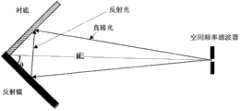
BG线图案也可以用激光干涉光刻技术(LIL)来实现,这是容易在大面积基板实现,而不需要一个掩膜版。激光干涉光刻技术(LIL)是在一个较大的区域基板上制造周期性的和准周期性图案的首选方法。BG line patterning can also be achieved using laser interference lithography (LIL), which is easily realized on large-area substrates without the need for a mask. Laser interference lithography (LIL) is the method of choice for fabricating periodic and quasi-periodic patterns on a large area substrate.
使用基于如图5所示的劳埃德干涉的装置。正规图案是由干涉激光束和反射激光束构成。由于第二束激光束是由一面非常接近基板的镜子形成,这样的设置与一个真正的双光束干涉设置相比,其对振动不太敏感。干涉图案的周期,以及在基板上的抗蚀层光栅记录,是由公式P=λ/(2sinθ)决定。使用363.8nm的光源,300纳米至1000纳米的周期,是可以很容易调出的。A setup based on Lloyd's interference as shown in Figure 5 was used. The regular pattern is formed by interfering laser beams and reflected laser beams. Since the second laser beam is formed by a mirror very close to the substrate, this setup is less sensitive to vibrations than a true two-beam interference setup. The period of the interference pattern, as well as the resist grating recording on the substrate, is determined by the formula P=λ/(2sinθ). Using a 363.8nm light source, the period from 300nm to 1000nm can be easily adjusted.
本实施例提供一种形成具有搭桥晶粒(BG)线的多晶硅薄膜的方法,包括:This embodiment provides a method for forming a polysilicon film with bridging grain (BG) lines, including:
1)在多晶硅薄膜上旋涂一层280nm的防反射涂层(ARC)并在175℃下硬烤,然后于ARC层上旋涂

2)在120℃硬烤后,样品被送到CF3000离子注入系统进行BG离子注入,经过BG离子注入后,PR胶在氧等离子体温度在100℃环境下30min剥夺去除。2) After hard-baking at 120°C, the sample was sent to the CF3000 ion implantation system for BG ion implantation. After BG ion implantation, the PR glue was deprived and removed in an oxygen plasma temperature of 100°C for 30 minutes.
本实施例得到的多晶硅薄膜可以被称为BG-poly-Si,可以作为TFT有源层使用。The polysilicon thin film obtained in this embodiment can be called BG-poly-Si, and can be used as a TFT active layer.
图7为使用LIL系统的正胶的SEM照片。应该指出,使用正性光刻胶形成光栅图案通常的PR线比沟槽狭窄,如图7所示。在这种情况下,离子注入和激活后,由于注入横向蔓延的现象和在激活过程中的扩散等原因,邻近BG线太容易发生短路。Fig. 7 is an SEM photo of a positive resist using the LIL system. It should be noted that using a positive photoresist to form a grating pattern usually has PR lines that are narrower than the trenches, as shown in FIG. 7 . In this case, after ion implantation and activation, the adjacent BG line is too prone to short circuit due to the phenomenon of implant lateral spread and diffusion during activation.
要解决这个问题,经LIL系统曝光后,可在氨气环境下90℃加热30分钟。然后样品被推进暴露在200mJ/cm2能源的UV光环境。最后,经过处理后,正胶变为负胶,显影后如图8所示,能够使后续形成的BG线间距增大,防止由于注入横向蔓延的现象和在激活过程中的扩散等原因使邻近的BG线短路。To solve this problem, after exposure by the LIL system, it can be heated at 90°C for 30 minutes in an ammonia atmosphere. The samples were then pushed forward and exposed to UV light with an energy source of 200mJ/cm2 . Finally, after processing, the positive resist becomes a negative resist, as shown in Figure 8 after development, which can increase the distance between the subsequently formed BG lines and prevent adjacent areas from being caused by injection lateral spread and diffusion during the activation process. The BG wire is shorted.
本实施例通过激光干涉光刻技术(LIL)生成BG图案和离子注入两个步骤,得到了由重复周期为300纳米至1000纳米的掺杂多晶硅平行线组成的BG线。In this embodiment, two steps of BG pattern generation and ion implantation by laser interference lithography (LIL) are used to obtain BG lines composed of doped polysilicon parallel lines with a repeat period of 300 nm to 1000 nm.
在其他实施例中,也可以在非晶硅上先形成BG线后再将非晶硅结晶成多晶硅,即BG线可以形成结晶前或后。In other embodiments, it is also possible to form the BG lines on the amorphous silicon first and then crystallize the amorphous silicon into polysilicon, that is, the BG lines can be formed before or after crystallization.
实施例3Example 3
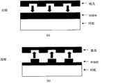
另一种能够实现了小尺寸的BG线图案的方式是纳米压印光刻(NIL)技术。NIL是一个简单的光刻工艺,具有成本低,高量产和高分辨率。它是通过在抗蚀剂上的印记的机械变形和后续工序来形成图案化。抗蚀剂的印记通常是由一个单体或聚合物制剂经过印制在热或紫外光固化过程中形成的。Another way to achieve small-sized BG line patterns is nanoimprint lithography (NIL) technology. NIL is a simple photolithographic process with low cost, high volume production and high resolution. It is patterned by mechanical deformation of imprints on resist and subsequent processes. Resist imprints are usually printed from a monomeric or polymeric formulation in a thermal or UV curing process.
NIL的原理如图9所示,将有着纳米尺度的起伏形状表面的硬模具压入在基板上聚合物材料,从而在聚合物材料上形成高低起伏的厚度对比。薄薄的聚合物材料的残积层是有意留模具突起部分的底下,作为柔软的缓冲层,以防止硬模具直接影响到基板,同时也有效保护模具表面细腻的纳米尺度的起伏形状表面以及设备表面。经过NIL处理之后,使BG形图案转移到基板上,然后再进行BG离子注入。The principle of NIL is shown in Figure 9. A hard mold with a nanoscale undulating surface is pressed into the polymer material on the substrate, thereby forming a thickness contrast of high and low undulations on the polymer material. The thin residual layer of polymer material is intentionally left under the protruding part of the mold as a soft buffer layer to prevent the hard mold from directly affecting the substrate, and also effectively protect the delicate nanoscale undulating shape of the mold surface and the surface of the device . After NIL treatment, the BG-shaped pattern is transferred to the substrate, and then BG ion implantation is performed.
实施例4Example 4
本实施例提供一种薄膜晶体管的制造方法,在准分子激光退火(ELA)多晶硅上形成BG线,然后利用该多晶硅制成TFT。This embodiment provides a method for manufacturing a thin film transistor, in which a BG line is formed on polysilicon by excimer laser annealing (ELA), and then a TFT is made by using the polysilicon.
与现有的低温多晶硅技术相比,ELA提供最好的质量,以及表现出最高的TFT特性。Compared to existing low-temperature polysilicon technologies, ELA offers the best quality and exhibits the highest TFT characteristics.
本实施例提供的薄膜晶体管的制造方法包括:The manufacturing method of the thin film transistor provided in this embodiment includes:
1)在玻璃基板上的ELA 4英寸多晶硅薄膜上沉积一层50nm的LTO层和一层50纳米的a-Si层,以减少从基板的反射光;1) Deposit a 50nm LTO layer and a 50nm a-Si layer on the ELA 4-inch polysilicon film on the glass substrate to reduce the reflected light from the substrate;
2)旋涂700纳米厚的PR 1075光刻胶,然后加热到90℃为1分钟;2) Spin-coat PR 1075 photoresist with a thickness of 700 nanometers, and then heat to 90°C for 1 minute;
3)光刻胶在曝光步进ASM PAS5000以波长为365nm的光曝光,形成BG线图案,BG线图案为宽度和间距均为0.5微米的平行线;3) The photoresist is exposed to light with a wavelength of 365nm in the exposure step ASM PAS5000 to form a BG line pattern, and the BG line pattern is parallel lines with a width and a spacing of 0.5 microns;
4)硬烤后,样品被送到CF3000,进行离子注入;4) After hard baking, the sample is sent to CF3000 for ion implantation;
5)剥离PR胶,蚀刻掉a-Si和LTO层;5) Peel off the PR glue, etch away the a-Si and LTO layers;
6)以AME8110活性离子蚀刻机干刻该部分掺杂BG-ELA多晶硅薄膜,形成有源岛;6) Use AME8110 reactive ion etching machine to dry-etch the part doped BG-ELA polysilicon film to form active islands;
7)用氧等离子除去光刻胶;7) removing photoresist with oxygen plasma;
8)用1%HF去除自然氧化层,然后用LPCVD法在425℃沉积70nm的低温氧化物(LTO)作为栅极绝缘层,沉积300nm的钛并图案化为栅电极;8) Use 1% HF to remove the natural oxide layer, then use LPCVD to deposit 70nm low-temperature oxide (LTO) at 425°C as a gate insulating layer, deposit 300nm titanium and pattern it as a gate electrode;
9)对P型沟道和N型沟道TFT分别以剂量4×10¹⁵/cm2掺入硼和磷,作为源极和漏极;9) Doping boron and phosphorus at a dose of 4×10¹⁵ /cm2 to the P-channel and N-channel TFTs, respectively, as the source and drain;
10)沉积一层500nm的LTO隔离层并同时激活掺杂物,打开接触孔,溅射700nm的铝-1%硅作为接触导线并图案化,接触导线的烧结是在420度FGA混合气体环境进行30分钟。10) Deposit a layer of 500nm LTO isolation layer and activate the dopant at the same time, open the contact hole, sputter 700nm aluminum-1% silicon as the contact wire and pattern it, and the sintering of the contact wire is carried out in a 420-degree FGA
图10所示为当Vds=-0.1V和Vds=-5V时,ELA TFT和不同掺杂剂量的BG-ELA TFT以Vgs为函数的转移特性曲线。P型-通道ELA的非BG和不同掺杂剂量BG的多晶硅薄膜晶体管的电气参数列于表
如图10(b)所示,当Vds=-5V,TFT在较高的电压下反向偏置,较高的BG掺杂量会导致更低的漏电流。这是因为,较高的BG掺杂剂量,在BG-TFT通道线的掺杂多晶硅和非掺杂多晶硅之间程现出更高的的势垒高度。因此,漏电流变小。As shown in FIG. 10( b ), when Vds =-5V, the TFT is reverse-biased at a higher voltage, and a higher BG doping amount will lead to a lower leakage current. This is because, with a higher BG doping dose, a higher barrier height appears between the doped polysilicon and the non-doped polysilicon of the BG-TFT channel line. Therefore, the leakage current becomes smaller.
图11(a)及(b)所示为,当Vds=-0.1V和Vds=-5V,以Vgs为函数,不同的掺杂量BG-ELA TFT与正常的ELA TFT的输出电流比(γ)图。我们可以发现,掺杂剂量2E15/cm2给人最大的改进是在亚阈值区(2区),但在反向区域(1区)也有比较大的比。5E14/cm2掺杂剂量在第2区域呈现第二大电流比率和在反向区域(1区)呈现最小电流比,这意味着在这一区域的漏电流最小。BG结构改变了BG-TFT的有效通道长度。为了更好地研究BG的效果,根据BG结构对沟道的调节,需对BG-ELA TFTs的IV曲线进行处理。在这里,我们假设,无论是否为BG结构,ELA-poly-Si的场效应迁移率在开态时保持不变。所以对不同掺杂量的BG-TFTs的最大场效应迁移率进行计算,并显示于表
因此,对BG掺杂5E14/cm2剂量,提供了最好的TFT性能,最低的漏电流,最小的Vth绝对值和亚阈值摆幅(S),最高的开/关比。Therefore, doping BG with adose of 5E14/cm2 provides the best TFT performance, the lowest leakage current, the smallest Vth absolute value and subthreshold swing (S), and the highest on/off ratio.
表1非BG与不同掺杂量BG结构的P型ELA多晶硅TFT电学参数Table 1 Electrical parameters of P-type ELA polysilicon TFT with non-BG and BG structures with different doping amounts

图12显示了P型沟道的一般ELA TFT和BG-ELA TFT的Vth和GIDL差异。测定的数据为均匀分布在超过4英寸的玻璃晶圆上的100个TFT。很显然,有着BG结构的TFT显示的GIDL比正常ELA的TFT低得多,从而BG-ELATFT的GIDL的均一性得以大大提高。同时,与一般的ELA TFT相比,BG-ELA TFT也展示出更小的Vth变化,以及Vth的绝对值。Figure 12 shows the difference in Vth and GIDL of a general ELA TFT and a BG-ELA TFT with a P-type channel. The measured data are 100 TFTs uniformly distributed on a glass wafer over 4 inches. Obviously, TFTs with BG structure showed much lower GIDL than TFTs with normal ELA, thus the uniformity of GIDL of BG-ELATFT was greatly improved. Meanwhile, compared with general ELA TFT, BG-ELA TFT also exhibits smaller Vth variation, and the absolute value of Vth .
B:N型沟道BG-ELA TFTB: N-channel BG-ELA TFT
图13(a)所示的为当Vds=-0.1V和Vds=-5V时,N型沟道BG结构与非BG结构ELA多晶硅薄膜晶体管的转移特性曲线。图14所示的是以Vgs为函数,N型沟道BG结构与非BG结构ELA多晶硅薄膜晶体管的输出电流比(γ)。Fig. 13(a) shows the transfer characteristic curves of N-channel BG structure and non-BG structure ELA polysilicon thin film transistors when Vds =-0.1V and Vds =-5V. FIG. 14 shows the output current ratio (γ) of the N-channel BG structure and the non-BG structure ELA polysilicon thin film transistor with Vgs as a function.
一个显著的改进是GIDL。BG TFT的漏电流是1.25pA/μm,这是一般的ELATFT在Vgs=-10V和Vds=5V时的大约1/170。如图13(a)所示,当Vds=5V,ELA的TFT显示了明显的漏电流和GIDL,而BG-ELA TFT的GIDL则明显受到抑制,特别是较高的反栅极偏置时。如图14所示,γ显着下降~5×10⁻³。从上面的对比,我们可以看到,随着BG结构的应用,大部分的TFT参数显着得到改善。A notable improvement is GIDL. The leakage current of the BG TFT is 1.25 pA/μm, which is about 1/170 of that of a general ELATFT at Vgs =-10V and Vds =5V. As shown in Fig. 13(a), when Vds = 5V, the TFT of ELA showed obvious leakage current and GIDL, while the GIDL of BG-ELA TFT was obviously suppressed, especially at higher back gate bias . As shown in Figure 14, γ dropped significantly by ~5×10⁻³ . From the above comparison, we can see that with the application of the BG structure, most of the TFT parameters are significantly improved.
对于所有的多晶硅TFTs的一个重要的问题是较大的关态电流。在以往文献中提出多晶硅TFTs的多种漏电流机制。从源极到漏极的空间电荷限流,载体经由靠近漏极耗尽区的晶界陷阱的热辐射,在耗尽区的场致热发射,寄生双极效应,漏极耗尽区的碰撞电离和耗尽区的带带隧道,是这些机制的一些解释。值得注意的是,多晶硅TFTs增大的关态电流主要与两个因素有关。第一个原因是因为加在栅极和漏极间的电压致使漏极的区域的高电场。当多晶硅TFTs在高反向栅电压和高漏电压时都偏向于关态区域,对于漏电流有较大影响的是在漏极区域将会形成高电场及一些场致增强生成机制。如图14所示,当Vds增加,漏电流显著提高。第二个原因是漏极附近的晶界陷阱密度。多晶硅后续退火和等离子钝化是两个用于降低晶界密度较好的方法,同时,可以减少漏电流。An important issue for all polysilicon TFTs is the large off-state current. Various leakage current mechanisms for polysilicon TFTs have been proposed in previous literature. Space charge current limitation from source to drain, thermal radiation of carriers via grain boundary traps near the drain depletion region, field thermal emission in the depletion region, parasitic bipolar effects, collisions in the drain depletion region Band tunneling in the ionization and depletion regions are some explanations for these mechanisms. It is worth noting that the increased off-state current of polysilicon TFTs is mainly related to two factors. The first reason is because of the high electric field in the region of the drain due to the voltage applied between the gate and the drain. While polysilicon TFTs are biased towards the off-state region at high reverse gate voltage and high drain voltage, what has a greater impact on leakage current is the formation of a high electric field and some field-enhancement generation mechanisms in the drain region. As shown in Figure 14, when Vds increases, the leakage current increases significantly. The second reason is the density of grain boundary traps near the drain. Post-annealing of polysilicon and plasma passivation are two better methods for reducing grain boundary density and, at the same time, reducing leakage current.
一个降低漏电的重要而且简单的途径是采用多栅结构。如图16(a)所示,以BG多晶硅作为有源通道的TFT横截面示意图,如图16(b)所示为多栅结构。因为通过多栅结构对漏电压的分割,可以降低漏极交界处的峰值电场。通常,可以通过多栅结构抑制漏电流。相同的解释也适用于BG多晶硅TFTs,也就是在通道内一系列的掺杂多晶硅和本征多晶硅。在掺杂BG线内的漂移电压可以减小漏极附近的峰值电场。使用ATLAS 2-D器件模拟器评价BG-TFT和传统TFT的反向栅极偏置电场。图15展示的是沿着TFT沟道的场分布。BG TFT里的BG结构可以减少峰值电场。能够降低由在漏极附近的峰值电场激励的漏电流。An important and simple way to reduce leakage is to use a multi-gate structure. As shown in FIG. 16(a), a schematic cross-sectional view of a TFT with BG polysilicon as an active channel, and a multi-gate structure as shown in FIG. 16(b). Because the drain voltage is divided by the multi-gate structure, the peak electric field at the junction of the drain can be reduced. In general, leakage current can be suppressed by a multi-gate structure. The same explanation applies to BG polysilicon TFTs, that is, a series of doped polysilicon and intrinsic polysilicon in the channel. The drift voltage in the doped BG line can reduce the peak electric field near the drain. The back gate bias electric field of BG-TFT and conventional TFT was evaluated using ATLAS 2-D device simulator. Figure 15 shows the field distribution along the TFT channel. The BG structure in BG TFT can reduce the peak electric field. The leakage current excited by the peak electric field near the drain can be reduced.
同多栅多晶硅TFTs相比BG多晶硅TFT还具有如下优点:Compared with multi-gate polysilicon TFTs, BG polysilicon TFTs also have the following advantages:
A:节约有源区域A: Save active area
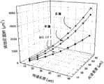
它们都可以降低因在漏极区域的高电场引起的漏电流。如图17所示,相同的W/L=20μm/12μm但栅极数目不同的SR-MILC多晶硅TFTs的漏电流。显而易见,可以通过增加栅极数目来降低漏电流。然而,在高栅漏电压下即使四栅TFT仍展现出明显的漏电流。也就是说,为了有效的抑制漏电流,栅极数目必须大于4。正如我们所知,在工业生产中,最小的栅极长度受曝光机精度所限制,对于多晶硅TFT结构,通常不会小于3μm。Both of them can reduce the leakage current caused by the high electric field in the drain region. As shown in Figure 17, the leakage current of SR-MILC polysilicon TFTs with the same W/L=20μm/12μm but different numbers of gates. Obviously, the leakage current can be reduced by increasing the number of gates. However, even quad-gate TFTs still exhibit significant leakage current at high gate-to-drain voltages. That is to say, in order to effectively suppress the leakage current, the number of gates must be greater than 4. As we know, in industrial production, the minimum gate length is limited by the precision of the exposure machine, and for polysilicon TFT structures, it is usually not less than 3 μm.
如前面所述,BG多晶硅TFT对开态电流的改进不仅因为通过掺杂的BG线减少有效沟道长度,而且通过BG结构减少晶界缺陷。如果考虑沟道长度的调节,一个W/L=10μm/12μm的BG-TFT可以提供与普通结构的W/L=20μm/12μm的TFT相同甚至更大的电流。如图18所示,对于一个4栅的多晶硅TFT,假设电路设计特征尺寸为5μm,分离栅极必须消耗20μm×21μm的有源区域。如图19所示,W或L的增加,多栅结构将会消耗额外的有源区域。所以,相较于普通的单栅TFT多栅结构会增加活动区域的消耗,而BG结构的TFT只需要普通单栅TFT的一半区域。这意味着多栅多晶硅TFT需要更多“有效”有源区域,将会降低多晶硅TFT LCD或底发射OLED的开口率,这将牺牲一些重要的性能对于多晶硅TFTs与非晶硅TFT相比。它不能应用于高分辨率和“低能耗”的显示器。As mentioned earlier, the improvement of the on-state current of BG polysilicon TFTs is not only due to the reduction of the effective channel length by the doped BG lines, but also the reduction of grain boundary defects by the BG structure. Considering the channel length adjustment, a BG-TFT with W/L=10μm/12μm can provide the same or even greater current than a TFT with W/L=20μm/12μm in common structure. As shown in Figure 18, for a polysilicon TFT with 4 gates, assuming that the circuit design feature size is 5 μm, the separated gates must consume an active area of 20 μm×21 μm. As shown in Figure 19, with the increase of W or L, the multi-gate structure will consume additional active area. Therefore, compared with the ordinary single-gate TFT, the multi-gate structure will increase the consumption of the active area, while the TFT with the BG structure only needs half the area of the ordinary single-gate TFT. This means that multi-gate polysilicon TFTs need more "active" active area, which will reduce the aperture ratio of polysilicon TFT LCDs or bottom-emitting OLEDs, which will sacrifice some important performance for polysilicon TFTs compared with amorphous silicon TFTs. It cannot be applied to high resolution and "low power" displays.
B:TFT性能的改进B: Improvement of TFT performance
为了得到很大改进的多晶硅TFTs,BG线间间距需要缩小至多晶硅晶粒尺寸大小,通常小于1μm。它可以通过激光干涉光刻和纳米压印光刻技术实现。然而,对于多栅结构,最小的栅极长度受限于光刻机固有精度对于在LTPS-TFT工厂的大面积曝光的最大精度为3μm。这意味着多栅结构不能达到实现改进的需要但是BG结构可以。In order to obtain greatly improved polysilicon TFTs, the spacing between BG lines needs to be reduced to the polysilicon grain size, usually less than 1 μm. It can be realized by laser interference lithography and nanoimprint lithography. However, for multi-gate structures, the minimum gate length is limited by the inherent precision of the lithography machine. The maximum precision for large-area exposure in LTPS-TFT fabs is 3 μm. This means that the multi-gate structure cannot achieve the improvement needed but the BG structure can.
尽管参照上述的实施例已对本发明作出具体描述,但是对于本领域的普通技术人员来说,以上实施例仅用以描述本发明的技术方案而非对本技术方法进行限制,本发明在应用上可以延伸为其他的修改、变化、应用和实施例,并且因此认为所有这样的修改、变化、应用、实施例都在本发明的精神和教导范围内。Although the present invention has been specifically described with reference to the above-mentioned embodiments, for those of ordinary skill in the art, the above embodiments are only used to describe the technical solutions of the present invention rather than limit the technical methods, and the present invention can be applied It extends to other modifications, changes, applications, and embodiments, and all such modifications, changes, applications, and embodiments are therefore considered to be within the spirit and teaching of the invention.
Claims (9)
Priority Applications (1)
| Application Number | Priority Date | Filing Date | Title |
|---|---|---|---|
| CN201110461865.4ACN103762174A (en) | 2011-08-23 | 2011-12-31 | Preparation method for thin-film transistor |
Applications Claiming Priority (5)
| Application Number | Priority Date | Filing Date | Title |
|---|---|---|---|
| CN201110243267 | 2011-08-23 | ||
| CN201110243267.X | 2011-08-23 | ||
| CN201110256340.7 | 2011-09-01 | ||
| CN201110256340 | 2011-09-01 | ||
| CN201110461865.4ACN103762174A (en) | 2011-08-23 | 2011-12-31 | Preparation method for thin-film transistor |
Publications (1)
| Publication Number | Publication Date |
|---|---|
| CN103762174Atrue CN103762174A (en) | 2014-04-30 |
Family
ID=46702891
Family Applications (17)
| Application Number | Title | Priority Date | Filing Date |
|---|---|---|---|
| CN2011103520076APendingCN102956500A (en) | 2011-08-23 | 2011-11-09 | Preparation method of polysilicon thin-film transistor |
| CN2011103519844APendingCN102956499A (en) | 2011-08-23 | 2011-11-09 | Preparation method of polysilicon film |
| CN201110351983XAPendingCN102956678A (en) | 2011-08-23 | 2011-11-09 | Polysilicon film |
| CN2011103519859APendingCN102956710A (en) | 2011-08-23 | 2011-11-09 | Mask metal induced crystallized polycrystalline silicon thin-film transistor |
| CN201120440884.4UExpired - Fee RelatedCN202405261U (en) | 2011-08-23 | 2011-11-09 | Mask MIC TFT film |
| CN201110461863.5APendingCN103762172A (en) | 2011-08-23 | 2011-12-31 | Preparation method of polysilicon thin film with bridged-grain structure |
| CN201110461883.2APendingCN103762176A (en) | 2011-08-23 | 2011-12-31 | Preparation method for polysilicon thin film with bridged crystal-grain structure |
| CN201110461873.9APendingCN103779209A (en) | 2011-08-23 | 2011-12-31 | Method for preparing polycrystalline silicon thin-film transistor |
| CN201120577247.1UExpired - Fee RelatedCN202405260U (en) | 2011-08-23 | 2011-12-31 | Active matrix display |
| CN201110461881.3APendingCN103762175A (en) | 2011-08-23 | 2011-12-31 | Preparation method for polysilicon thin film with bridged crystal-grain structure |
| CN201110461875.8APendingCN103779420A (en) | 2011-08-23 | 2011-12-31 | Polycrystalline silicon thin-film transistor with bridging grain structure |
| CN201110461864.XAPendingCN103762173A (en) | 2011-08-23 | 2011-12-31 | Method for preparing polysilicon thin film |
| CN201110461884.7APendingCN103779391A (en) | 2011-08-23 | 2011-12-31 | Polycrystalline silicon thin film with bridging grain structure and preparation method thereof |
| CN201110461865.4APendingCN103762174A (en) | 2011-08-23 | 2011-12-31 | Preparation method for thin-film transistor |
| CN2012100513018APendingCN102955307A (en) | 2011-08-23 | 2012-03-01 | Field sequential color liquid crystal display based on polycrystalline silicon thin film transistor |
| CN2012100512443APendingCN102956648A (en) | 2011-08-23 | 2012-03-01 | Active matrix rear panel with liquid crystal display |
| CN2012100512458APendingCN102956549A (en) | 2011-08-23 | 2012-03-01 | Manufacturing method of active matrix backing plate of field sequential color liquid crystal display |
Family Applications Before (13)
| Application Number | Title | Priority Date | Filing Date |
|---|---|---|---|
| CN2011103520076APendingCN102956500A (en) | 2011-08-23 | 2011-11-09 | Preparation method of polysilicon thin-film transistor |
| CN2011103519844APendingCN102956499A (en) | 2011-08-23 | 2011-11-09 | Preparation method of polysilicon film |
| CN201110351983XAPendingCN102956678A (en) | 2011-08-23 | 2011-11-09 | Polysilicon film |
| CN2011103519859APendingCN102956710A (en) | 2011-08-23 | 2011-11-09 | Mask metal induced crystallized polycrystalline silicon thin-film transistor |
| CN201120440884.4UExpired - Fee RelatedCN202405261U (en) | 2011-08-23 | 2011-11-09 | Mask MIC TFT film |
| CN201110461863.5APendingCN103762172A (en) | 2011-08-23 | 2011-12-31 | Preparation method of polysilicon thin film with bridged-grain structure |
| CN201110461883.2APendingCN103762176A (en) | 2011-08-23 | 2011-12-31 | Preparation method for polysilicon thin film with bridged crystal-grain structure |
| CN201110461873.9APendingCN103779209A (en) | 2011-08-23 | 2011-12-31 | Method for preparing polycrystalline silicon thin-film transistor |
| CN201120577247.1UExpired - Fee RelatedCN202405260U (en) | 2011-08-23 | 2011-12-31 | Active matrix display |
| CN201110461881.3APendingCN103762175A (en) | 2011-08-23 | 2011-12-31 | Preparation method for polysilicon thin film with bridged crystal-grain structure |
| CN201110461875.8APendingCN103779420A (en) | 2011-08-23 | 2011-12-31 | Polycrystalline silicon thin-film transistor with bridging grain structure |
| CN201110461864.XAPendingCN103762173A (en) | 2011-08-23 | 2011-12-31 | Method for preparing polysilicon thin film |
| CN201110461884.7APendingCN103779391A (en) | 2011-08-23 | 2011-12-31 | Polycrystalline silicon thin film with bridging grain structure and preparation method thereof |
Family Applications After (3)
| Application Number | Title | Priority Date | Filing Date |
|---|---|---|---|
| CN2012100513018APendingCN102955307A (en) | 2011-08-23 | 2012-03-01 | Field sequential color liquid crystal display based on polycrystalline silicon thin film transistor |
| CN2012100512443APendingCN102956648A (en) | 2011-08-23 | 2012-03-01 | Active matrix rear panel with liquid crystal display |
| CN2012100512458APendingCN102956549A (en) | 2011-08-23 | 2012-03-01 | Manufacturing method of active matrix backing plate of field sequential color liquid crystal display |
Country Status (1)
| Country | Link |
|---|---|
| CN (17) | CN102956500A (en) |
Cited By (1)
| Publication number | Priority date | Publication date | Assignee | Title |
|---|---|---|---|---|
| CN106328506A (en)* | 2016-08-31 | 2017-01-11 | 上海华力微电子有限公司 | Method for reducing peeling risk of photoresist of ion implantation layer |
Families Citing this family (20)
| Publication number | Priority date | Publication date | Assignee | Title |
|---|---|---|---|---|
| CN103151388B (en)* | 2013-03-05 | 2015-11-11 | 京东方科技集团股份有限公司 | A kind of polycrystalline SiTFT and preparation method thereof, array base palte |
| CN103235439B (en)* | 2013-04-08 | 2015-08-12 | 北京京东方光电科技有限公司 | A kind of to box substrate and preparation method, touch-screen, display device |
| CN104282546A (en)* | 2013-07-08 | 2015-01-14 | 上海和辉光电有限公司 | Method for improving homogeneity of polycrystalline silicon layer |
| CN103700688B (en)* | 2013-12-23 | 2016-03-30 | 京东方科技集团股份有限公司 | Color membrane substrates and preparation method thereof, display unit |
| CN103700698B (en)* | 2013-12-30 | 2016-06-15 | 北京京东方光电科技有限公司 | The preparation method of a kind of thin film transistor, thin film transistor and display panel |
| US9793361B2 (en) | 2014-09-10 | 2017-10-17 | Boe Technology Group Co., Ltd. | Thin film transistor, array substrate and display device |
| CN104241395B (en)* | 2014-09-10 | 2017-02-15 | 京东方科技集团股份有限公司 | Thin film transistor, array substrate and displaying device |
| CN105514023B (en)* | 2014-09-22 | 2018-07-24 | 上海和辉光电有限公司 | A kind of contact hole interface processing method |
| CN104505340B (en)* | 2014-11-28 | 2017-12-26 | 信利(惠州)智能显示有限公司 | A kind of preparation method of low-temperature polysilicon film |
| CN106033707A (en)* | 2015-03-10 | 2016-10-19 | 上海和辉光电有限公司 | Preparation method for polysilicon film |
| CN105575974B (en)* | 2015-12-14 | 2018-08-14 | 深圳市华星光电技术有限公司 | The production method of low temperature polycrystalline silicon TFT backplate |
| CN106298802B (en)* | 2016-08-16 | 2019-05-07 | 武汉华星光电技术有限公司 | A kind of LTPS array substrate and manufacturing method, display panel |
| CN106601873B (en)* | 2016-12-16 | 2018-06-29 | 苏州腾晖光伏技术有限公司 | A kind of spin coating device for CZTS films and the method for preparing CZTS batteries |
| AU2017391778B2 (en)* | 2017-01-04 | 2022-09-29 | Shih-Hsien Tseng | Pixel unit structure and manufacturing method thereof |
| CN106876479B (en) | 2017-04-19 | 2020-03-06 | 京东方科技集团股份有限公司 | Thin film transistor and preparation method thereof, array substrate and preparation method thereof, and display panel |
| CN109742028B (en)* | 2018-12-25 | 2021-04-02 | 惠科股份有限公司 | Manufacturing method of thin film transistor, thin film transistor and display panel |
| DE102019100312A1 (en)* | 2019-01-08 | 2020-07-09 | Parcan NanoTech Co. Ltd. | Controlled ion implantation substrate and method of making a controlled ion implantation substrate |
| CN112736087B (en)* | 2019-10-10 | 2024-03-05 | 京东方科技集团股份有限公司 | Manufacturing method of array substrate, array substrate and display panel |
| CN110660869A (en)* | 2019-10-27 | 2020-01-07 | 南京飞芯电子科技有限公司 | Method for forming enhancement mode field effect transistor |
| CN112563197B (en)* | 2020-11-24 | 2022-03-22 | 惠科股份有限公司 | Active switch, manufacturing method thereof and display panel |
Citations (5)
| Publication number | Priority date | Publication date | Assignee | Title |
|---|---|---|---|---|
| JPH11354800A (en)* | 1998-06-04 | 1999-12-24 | Hitachi Ltd | Thin film transistor, method for forming the same, and liquid crystal display device |
| JP2000133807A (en)* | 1998-10-22 | 2000-05-12 | Seiko Epson Corp | Polycrystalline silicon thin film transistor |
| US6903372B1 (en)* | 1999-10-29 | 2005-06-07 | Hitachi, Ltd. | Semiconductor device, method of making the same and liquid crystal display device |
| CN101681930A (en)* | 2007-06-22 | 2010-03-24 | 香港科技大学 | Polycrystalline silicon thin film transistor with bridged grain structure |
| CN101814438A (en)* | 2010-05-17 | 2010-08-25 | 广东中显科技有限公司 | Preparation method of thin film transistor based on induced longitudinal crystallization polycrystalline silicon |
Family Cites Families (22)
| Publication number | Priority date | Publication date | Assignee | Title |
|---|---|---|---|---|
| JPS5783047A (en)* | 1980-11-10 | 1982-05-24 | Matsushita Electric Ind Co Ltd | Polycrystalline semiconductor resistor |
| TW520072U (en)* | 1991-07-08 | 2003-02-01 | Samsung Electronics Co Ltd | A semiconductor device having a multi-layer metal contact |
| JPH06104438A (en)* | 1992-09-22 | 1994-04-15 | Casio Comput Co Ltd | Thin film transistor |
| JPH08139335A (en)* | 1994-11-14 | 1996-05-31 | Casio Comput Co Ltd | Method for manufacturing thin film transistor |
| US6108058A (en)* | 1997-04-30 | 2000-08-22 | Tohoku Techno-Brains Corporation | Field sequential Pi cell LCD with compensator |
| JP4436469B2 (en)* | 1998-09-30 | 2010-03-24 | 三洋電機株式会社 | Semiconductor device |
| JP2000208771A (en)* | 1999-01-11 | 2000-07-28 | Hitachi Ltd | Semiconductor device, liquid crystal display device, and manufacturing method thereof |
| JP3873811B2 (en)* | 2002-05-15 | 2007-01-31 | 日本電気株式会社 | Manufacturing method of semiconductor device |
| KR100930362B1 (en)* | 2002-11-04 | 2009-12-08 | 엘지디스플레이 주식회사 | Polycrystalline Silicon Film Formation Method And Manufacturing Method Of Thin Film Transistor Including The Same |
| KR100577795B1 (en)* | 2003-12-30 | 2006-05-11 | 비오이 하이디스 테크놀로지 주식회사 | Polycrystalline Silicon Film Formation Method |
| TWI266427B (en)* | 2004-06-01 | 2006-11-11 | Yamanashi Tlo Co Ltd | Field-effect transistor and method of manufacturing same |
| TWI241027B (en)* | 2004-09-30 | 2005-10-01 | Ind Tech Res Inst | Method of preparing electronic device |
| US8088676B2 (en)* | 2005-04-28 | 2012-01-03 | The Hong Kong University Of Science And Technology | Metal-induced crystallization of amorphous silicon, polycrystalline silicon thin films produced thereby and thin film transistors produced therefrom |
| CN100592174C (en)* | 2005-05-21 | 2010-02-24 | 香港科技大学 | Transflective liquid crystal device and preparation method thereof |
| US7790580B2 (en)* | 2006-03-13 | 2010-09-07 | Hong Kong University Of Science And Technology | Metal-induced crystallization of amorphous silicon in thin film transistors |
| JP5295529B2 (en)* | 2007-08-13 | 2013-09-18 | 株式会社ジャパンディスプレイ | Semiconductor device |
| CN101834211A (en)* | 2010-02-09 | 2010-09-15 | 广东中显科技有限公司 | Polycrystalline silicon thin film based on metal induction |
| CN101834138A (en)* | 2010-02-09 | 2010-09-15 | 广东中显科技有限公司 | Method for preparing transistor device of crystallized thin film |
| CN101853784B (en)* | 2010-05-17 | 2012-07-04 | 广东中显科技有限公司 | Method for transversely inducing and crystallizing low-temperature polycrystalline silicon film |
| CN101819999A (en)* | 2010-05-17 | 2010-09-01 | 广东中显科技有限公司 | Multilayer film structure for transverse induced crystallization of low-temperature poly-silicon film |
| CN102129962A (en)* | 2010-10-28 | 2011-07-20 | 广东中显科技有限公司 | Controllable method for manufacturing polysilicon thin film through metal induction |
| CN102082098A (en)* | 2010-12-15 | 2011-06-01 | 四川虹视显示技术有限公司 | Method for producing low-temperature polysilicon thin-film transistor |
- 2011
- 2011-11-09CNCN2011103520076Apatent/CN102956500A/enactivePending
- 2011-11-09CNCN2011103519844Apatent/CN102956499A/enactivePending
- 2011-11-09CNCN201110351983XApatent/CN102956678A/enactivePending
- 2011-11-09CNCN2011103519859Apatent/CN102956710A/enactivePending
- 2011-11-09CNCN201120440884.4Upatent/CN202405261U/ennot_activeExpired - Fee Related
- 2011-12-31CNCN201110461863.5Apatent/CN103762172A/enactivePending
- 2011-12-31CNCN201110461883.2Apatent/CN103762176A/enactivePending
- 2011-12-31CNCN201110461873.9Apatent/CN103779209A/enactivePending
- 2011-12-31CNCN201120577247.1Upatent/CN202405260U/ennot_activeExpired - Fee Related
- 2011-12-31CNCN201110461881.3Apatent/CN103762175A/enactivePending
- 2011-12-31CNCN201110461875.8Apatent/CN103779420A/enactivePending
- 2011-12-31CNCN201110461864.XApatent/CN103762173A/enactivePending
- 2011-12-31CNCN201110461884.7Apatent/CN103779391A/enactivePending
- 2011-12-31CNCN201110461865.4Apatent/CN103762174A/enactivePending
- 2012
- 2012-03-01CNCN2012100513018Apatent/CN102955307A/enactivePending
- 2012-03-01CNCN2012100512443Apatent/CN102956648A/enactivePending
- 2012-03-01CNCN2012100512458Apatent/CN102956549A/enactivePending
Patent Citations (5)
| Publication number | Priority date | Publication date | Assignee | Title |
|---|---|---|---|---|
| JPH11354800A (en)* | 1998-06-04 | 1999-12-24 | Hitachi Ltd | Thin film transistor, method for forming the same, and liquid crystal display device |
| JP2000133807A (en)* | 1998-10-22 | 2000-05-12 | Seiko Epson Corp | Polycrystalline silicon thin film transistor |
| US6903372B1 (en)* | 1999-10-29 | 2005-06-07 | Hitachi, Ltd. | Semiconductor device, method of making the same and liquid crystal display device |
| CN101681930A (en)* | 2007-06-22 | 2010-03-24 | 香港科技大学 | Polycrystalline silicon thin film transistor with bridged grain structure |
| CN101814438A (en)* | 2010-05-17 | 2010-08-25 | 广东中显科技有限公司 | Preparation method of thin film transistor based on induced longitudinal crystallization polycrystalline silicon |
Cited By (2)
| Publication number | Priority date | Publication date | Assignee | Title |
|---|---|---|---|---|
| CN106328506A (en)* | 2016-08-31 | 2017-01-11 | 上海华力微电子有限公司 | Method for reducing peeling risk of photoresist of ion implantation layer |
| CN106328506B (en)* | 2016-08-31 | 2020-04-10 | 上海华力微电子有限公司 | Method for reducing photoresist stripping risk of ion implantation layer |
Also Published As
| Publication number | Publication date |
|---|---|
| CN102956500A (en) | 2013-03-06 |
| CN102956499A (en) | 2013-03-06 |
| CN103779391A (en) | 2014-05-07 |
| CN103762176A (en) | 2014-04-30 |
| CN103779209A (en) | 2014-05-07 |
| CN103779420A (en) | 2014-05-07 |
| CN103762172A (en) | 2014-04-30 |
| CN103762173A (en) | 2014-04-30 |
| CN102956648A (en) | 2013-03-06 |
| CN102955307A (en) | 2013-03-06 |
| CN103762175A (en) | 2014-04-30 |
| CN202405260U (en) | 2012-08-29 |
| CN102956710A (en) | 2013-03-06 |
| CN102956678A (en) | 2013-03-06 |
| CN202405261U (en) | 2012-08-29 |
| CN102956549A (en) | 2013-03-06 |
Similar Documents
| Publication | Publication Date | Title |
|---|---|---|
| CN103762174A (en) | Preparation method for thin-film transistor | |
| US8426865B2 (en) | Polycrystalline silicon thin film transistors with bridged-grain structures | |
| CN104282696B (en) | A kind of array substrate and preparation method thereof, display device | |
| CN105702623B (en) | Manufacturing method of TFT array substrate | |
| CN104576399B (en) | A kind of thin film transistor (TFT) and its manufacture method | |
| CN105097841B (en) | The production method and TFT substrate of TFT substrate | |
| WO2015123903A1 (en) | Low-temperature polycrystalline silicon thin-film transistor, array substrate and manufacturing method therefor | |
| CN105304500B (en) | N-type TFT preparation method | |
| CN104240633A (en) | Thin film transistor and active matrix organic light emitting diode assembly and manufacturing method thereof | |
| CN104538458A (en) | Display device, array substrate, thin film transistor and fabricating method thereof | |
| CN106847703A (en) | The manufacture method and display device of low-temperature polysilicon film transistor | |
| CN107170759A (en) | A kind of array base palte and preparation method thereof, display device | |
| CN103000531A (en) | Manufacturing method for low-temperature polycrystalline silicon thin film transistor | |
| CN103367456B (en) | Thin-film transistor and manufacture method thereof | |
| US10340365B2 (en) | Method of manufacturing a thin film transistor | |
| CN106952963B (en) | A kind of thin film transistor (TFT) and production method, array substrate, display device | |
| CN105551967A (en) | Manufacturing method of N-type thin film transistor | |
| CN204130536U (en) | A kind of array base palte and display unit | |
| CN104465509A (en) | OLED display device array substrate and preparation method thereof | |
| CN102931137B (en) | LTPS-TFT (Low Temperature Poly Silicon-Thin Film Transistor) array substrate and manufacture method thereof, and display device | |
| CN115440823A (en) | Thin film transistor, preparation method, array substrate and display device | |
| CN103762167A (en) | Bridged-grain polysilicon thin film transistor and manufacturing method thereof | |
| CN101728436A (en) | Element of thin film transistor and manufacturing method thereof | |
| CN103762165A (en) | Simplified manufacturing method of bridged-grain polysilicon thin film transistor | |
| CN103762168A (en) | Manufacture method of bottom gate thin film transistor |
Legal Events
| Date | Code | Title | Description |
|---|---|---|---|
| C06 | Publication | ||
| PB01 | Publication | ||
| C10 | Entry into substantive examination | ||
| SE01 | Entry into force of request for substantive examination | ||
| C02 | Deemed withdrawal of patent application after publication (patent law 2001) | ||
| WD01 | Invention patent application deemed withdrawn after publication | Application publication date:20140430 |