CN103760707A - Array substrate, liquid crystal display panel and display device - Google Patents
Array substrate, liquid crystal display panel and display deviceDownload PDFInfo
- Publication number
- CN103760707A CN103760707ACN201410010209.6ACN201410010209ACN103760707ACN 103760707 ACN103760707 ACN 103760707ACN 201410010209 ACN201410010209 ACN 201410010209ACN 103760707 ACN103760707 ACN 103760707A
- Authority
- CN
- China
- Prior art keywords
- photovoltaic
- array substrate
- photovoltaic cell
- cell assembly
- base substrate
- Prior art date
- Legal status (The legal status is an assumption and is not a legal conclusion. Google has not performed a legal analysis and makes no representation as to the accuracy of the status listed.)
- Pending
Links
Images


Classifications
- G—PHYSICS
- G02—OPTICS
- G02F—OPTICAL DEVICES OR ARRANGEMENTS FOR THE CONTROL OF LIGHT BY MODIFICATION OF THE OPTICAL PROPERTIES OF THE MEDIA OF THE ELEMENTS INVOLVED THEREIN; NON-LINEAR OPTICS; FREQUENCY-CHANGING OF LIGHT; OPTICAL LOGIC ELEMENTS; OPTICAL ANALOGUE/DIGITAL CONVERTERS
- G02F1/00—Devices or arrangements for the control of the intensity, colour, phase, polarisation or direction of light arriving from an independent light source, e.g. switching, gating or modulating; Non-linear optics
- G02F1/01—Devices or arrangements for the control of the intensity, colour, phase, polarisation or direction of light arriving from an independent light source, e.g. switching, gating or modulating; Non-linear optics for the control of the intensity, phase, polarisation or colour
- G02F1/13—Devices or arrangements for the control of the intensity, colour, phase, polarisation or direction of light arriving from an independent light source, e.g. switching, gating or modulating; Non-linear optics for the control of the intensity, phase, polarisation or colour based on liquid crystals, e.g. single liquid crystal display cells
- G02F1/133—Constructional arrangements; Operation of liquid crystal cells; Circuit arrangements
- G02F1/13306—Circuit arrangements or driving methods for the control of single liquid crystal cells
- G02F1/13318—Circuits comprising a photodetector
- G—PHYSICS
- G02—OPTICS
- G02F—OPTICAL DEVICES OR ARRANGEMENTS FOR THE CONTROL OF LIGHT BY MODIFICATION OF THE OPTICAL PROPERTIES OF THE MEDIA OF THE ELEMENTS INVOLVED THEREIN; NON-LINEAR OPTICS; FREQUENCY-CHANGING OF LIGHT; OPTICAL LOGIC ELEMENTS; OPTICAL ANALOGUE/DIGITAL CONVERTERS
- G02F1/00—Devices or arrangements for the control of the intensity, colour, phase, polarisation or direction of light arriving from an independent light source, e.g. switching, gating or modulating; Non-linear optics
- G02F1/01—Devices or arrangements for the control of the intensity, colour, phase, polarisation or direction of light arriving from an independent light source, e.g. switching, gating or modulating; Non-linear optics for the control of the intensity, phase, polarisation or colour
- G02F1/13—Devices or arrangements for the control of the intensity, colour, phase, polarisation or direction of light arriving from an independent light source, e.g. switching, gating or modulating; Non-linear optics for the control of the intensity, phase, polarisation or colour based on liquid crystals, e.g. single liquid crystal display cells
- G02F1/1313—Devices or arrangements for the control of the intensity, colour, phase, polarisation or direction of light arriving from an independent light source, e.g. switching, gating or modulating; Non-linear optics for the control of the intensity, phase, polarisation or colour based on liquid crystals, e.g. single liquid crystal display cells specially adapted for a particular application
- G—PHYSICS
- G02—OPTICS
- G02F—OPTICAL DEVICES OR ARRANGEMENTS FOR THE CONTROL OF LIGHT BY MODIFICATION OF THE OPTICAL PROPERTIES OF THE MEDIA OF THE ELEMENTS INVOLVED THEREIN; NON-LINEAR OPTICS; FREQUENCY-CHANGING OF LIGHT; OPTICAL LOGIC ELEMENTS; OPTICAL ANALOGUE/DIGITAL CONVERTERS
- G02F1/00—Devices or arrangements for the control of the intensity, colour, phase, polarisation or direction of light arriving from an independent light source, e.g. switching, gating or modulating; Non-linear optics
- G02F1/01—Devices or arrangements for the control of the intensity, colour, phase, polarisation or direction of light arriving from an independent light source, e.g. switching, gating or modulating; Non-linear optics for the control of the intensity, phase, polarisation or colour
- G02F1/13—Devices or arrangements for the control of the intensity, colour, phase, polarisation or direction of light arriving from an independent light source, e.g. switching, gating or modulating; Non-linear optics for the control of the intensity, phase, polarisation or colour based on liquid crystals, e.g. single liquid crystal display cells
- G02F1/133—Constructional arrangements; Operation of liquid crystal cells; Circuit arrangements
- G02F1/1333—Constructional arrangements; Manufacturing methods
- G02F1/1335—Structural association of cells with optical devices, e.g. polarisers or reflectors
- G02F1/133553—Reflecting elements
- G02F1/133555—Transflectors
- G—PHYSICS
- G02—OPTICS
- G02F—OPTICAL DEVICES OR ARRANGEMENTS FOR THE CONTROL OF LIGHT BY MODIFICATION OF THE OPTICAL PROPERTIES OF THE MEDIA OF THE ELEMENTS INVOLVED THEREIN; NON-LINEAR OPTICS; FREQUENCY-CHANGING OF LIGHT; OPTICAL LOGIC ELEMENTS; OPTICAL ANALOGUE/DIGITAL CONVERTERS
- G02F1/00—Devices or arrangements for the control of the intensity, colour, phase, polarisation or direction of light arriving from an independent light source, e.g. switching, gating or modulating; Non-linear optics
- G02F1/01—Devices or arrangements for the control of the intensity, colour, phase, polarisation or direction of light arriving from an independent light source, e.g. switching, gating or modulating; Non-linear optics for the control of the intensity, phase, polarisation or colour
- G02F1/13—Devices or arrangements for the control of the intensity, colour, phase, polarisation or direction of light arriving from an independent light source, e.g. switching, gating or modulating; Non-linear optics for the control of the intensity, phase, polarisation or colour based on liquid crystals, e.g. single liquid crystal display cells
- G02F1/133—Constructional arrangements; Operation of liquid crystal cells; Circuit arrangements
- G02F1/1333—Constructional arrangements; Manufacturing methods
- G02F1/1343—Electrodes
- G02F1/134309—Electrodes characterised by their geometrical arrangement
- G—PHYSICS
- G02—OPTICS
- G02F—OPTICAL DEVICES OR ARRANGEMENTS FOR THE CONTROL OF LIGHT BY MODIFICATION OF THE OPTICAL PROPERTIES OF THE MEDIA OF THE ELEMENTS INVOLVED THEREIN; NON-LINEAR OPTICS; FREQUENCY-CHANGING OF LIGHT; OPTICAL LOGIC ELEMENTS; OPTICAL ANALOGUE/DIGITAL CONVERTERS
- G02F1/00—Devices or arrangements for the control of the intensity, colour, phase, polarisation or direction of light arriving from an independent light source, e.g. switching, gating or modulating; Non-linear optics
- G02F1/01—Devices or arrangements for the control of the intensity, colour, phase, polarisation or direction of light arriving from an independent light source, e.g. switching, gating or modulating; Non-linear optics for the control of the intensity, phase, polarisation or colour
- G02F1/13—Devices or arrangements for the control of the intensity, colour, phase, polarisation or direction of light arriving from an independent light source, e.g. switching, gating or modulating; Non-linear optics for the control of the intensity, phase, polarisation or colour based on liquid crystals, e.g. single liquid crystal display cells
- G02F1/133—Constructional arrangements; Operation of liquid crystal cells; Circuit arrangements
- G02F1/1333—Constructional arrangements; Manufacturing methods
- G02F1/1343—Electrodes
- G02F1/13439—Electrodes characterised by their electrical, optical, physical properties; materials therefor; method of making
- G—PHYSICS
- G02—OPTICS
- G02F—OPTICAL DEVICES OR ARRANGEMENTS FOR THE CONTROL OF LIGHT BY MODIFICATION OF THE OPTICAL PROPERTIES OF THE MEDIA OF THE ELEMENTS INVOLVED THEREIN; NON-LINEAR OPTICS; FREQUENCY-CHANGING OF LIGHT; OPTICAL LOGIC ELEMENTS; OPTICAL ANALOGUE/DIGITAL CONVERTERS
- G02F1/00—Devices or arrangements for the control of the intensity, colour, phase, polarisation or direction of light arriving from an independent light source, e.g. switching, gating or modulating; Non-linear optics
- G02F1/01—Devices or arrangements for the control of the intensity, colour, phase, polarisation or direction of light arriving from an independent light source, e.g. switching, gating or modulating; Non-linear optics for the control of the intensity, phase, polarisation or colour
- G02F1/13—Devices or arrangements for the control of the intensity, colour, phase, polarisation or direction of light arriving from an independent light source, e.g. switching, gating or modulating; Non-linear optics for the control of the intensity, phase, polarisation or colour based on liquid crystals, e.g. single liquid crystal display cells
- G02F1/133—Constructional arrangements; Operation of liquid crystal cells; Circuit arrangements
- G02F1/136—Liquid crystal cells structurally associated with a semi-conducting layer or substrate, e.g. cells forming part of an integrated circuit
- G02F1/1362—Active matrix addressed cells
- G02F1/1368—Active matrix addressed cells in which the switching element is a three-electrode device
- H—ELECTRICITY
- H01—ELECTRIC ELEMENTS
- H01L—SEMICONDUCTOR DEVICES NOT COVERED BY CLASS H10
- H01L25/00—Assemblies consisting of a plurality of semiconductor or other solid state devices
- H01L25/16—Assemblies consisting of a plurality of semiconductor or other solid state devices the devices being of types provided for in two or more different subclasses of H10B, H10D, H10F, H10H, H10K or H10N, e.g. forming hybrid circuits
- H01L25/167—Assemblies consisting of a plurality of semiconductor or other solid state devices the devices being of types provided for in two or more different subclasses of H10B, H10D, H10F, H10H, H10K or H10N, e.g. forming hybrid circuits comprising optoelectronic devices, e.g. LED, photodiodes
- H—ELECTRICITY
- H10—SEMICONDUCTOR DEVICES; ELECTRIC SOLID-STATE DEVICES NOT OTHERWISE PROVIDED FOR
- H10D—INORGANIC ELECTRIC SEMICONDUCTOR DEVICES
- H10D86/00—Integrated devices formed in or on insulating or conducting substrates, e.g. formed in silicon-on-insulator [SOI] substrates or on stainless steel or glass substrates
- G—PHYSICS
- G02—OPTICS
- G02F—OPTICAL DEVICES OR ARRANGEMENTS FOR THE CONTROL OF LIGHT BY MODIFICATION OF THE OPTICAL PROPERTIES OF THE MEDIA OF THE ELEMENTS INVOLVED THEREIN; NON-LINEAR OPTICS; FREQUENCY-CHANGING OF LIGHT; OPTICAL LOGIC ELEMENTS; OPTICAL ANALOGUE/DIGITAL CONVERTERS
- G02F1/00—Devices or arrangements for the control of the intensity, colour, phase, polarisation or direction of light arriving from an independent light source, e.g. switching, gating or modulating; Non-linear optics
- G02F1/01—Devices or arrangements for the control of the intensity, colour, phase, polarisation or direction of light arriving from an independent light source, e.g. switching, gating or modulating; Non-linear optics for the control of the intensity, phase, polarisation or colour
- G02F1/13—Devices or arrangements for the control of the intensity, colour, phase, polarisation or direction of light arriving from an independent light source, e.g. switching, gating or modulating; Non-linear optics for the control of the intensity, phase, polarisation or colour based on liquid crystals, e.g. single liquid crystal display cells
- G02F1/133—Constructional arrangements; Operation of liquid crystal cells; Circuit arrangements
- G02F1/13306—Circuit arrangements or driving methods for the control of single liquid crystal cells
- G02F1/13324—Circuits comprising solar cells
- G—PHYSICS
- G02—OPTICS
- G02F—OPTICAL DEVICES OR ARRANGEMENTS FOR THE CONTROL OF LIGHT BY MODIFICATION OF THE OPTICAL PROPERTIES OF THE MEDIA OF THE ELEMENTS INVOLVED THEREIN; NON-LINEAR OPTICS; FREQUENCY-CHANGING OF LIGHT; OPTICAL LOGIC ELEMENTS; OPTICAL ANALOGUE/DIGITAL CONVERTERS
- G02F1/00—Devices or arrangements for the control of the intensity, colour, phase, polarisation or direction of light arriving from an independent light source, e.g. switching, gating or modulating; Non-linear optics
- G02F1/01—Devices or arrangements for the control of the intensity, colour, phase, polarisation or direction of light arriving from an independent light source, e.g. switching, gating or modulating; Non-linear optics for the control of the intensity, phase, polarisation or colour
- G02F1/13—Devices or arrangements for the control of the intensity, colour, phase, polarisation or direction of light arriving from an independent light source, e.g. switching, gating or modulating; Non-linear optics for the control of the intensity, phase, polarisation or colour based on liquid crystals, e.g. single liquid crystal display cells
- G02F1/133—Constructional arrangements; Operation of liquid crystal cells; Circuit arrangements
- G02F1/1333—Constructional arrangements; Manufacturing methods
- G02F1/133357—Planarisation layers
- G—PHYSICS
- G02—OPTICS
- G02F—OPTICAL DEVICES OR ARRANGEMENTS FOR THE CONTROL OF LIGHT BY MODIFICATION OF THE OPTICAL PROPERTIES OF THE MEDIA OF THE ELEMENTS INVOLVED THEREIN; NON-LINEAR OPTICS; FREQUENCY-CHANGING OF LIGHT; OPTICAL LOGIC ELEMENTS; OPTICAL ANALOGUE/DIGITAL CONVERTERS
- G02F1/00—Devices or arrangements for the control of the intensity, colour, phase, polarisation or direction of light arriving from an independent light source, e.g. switching, gating or modulating; Non-linear optics
- G02F1/01—Devices or arrangements for the control of the intensity, colour, phase, polarisation or direction of light arriving from an independent light source, e.g. switching, gating or modulating; Non-linear optics for the control of the intensity, phase, polarisation or colour
- G02F1/13—Devices or arrangements for the control of the intensity, colour, phase, polarisation or direction of light arriving from an independent light source, e.g. switching, gating or modulating; Non-linear optics for the control of the intensity, phase, polarisation or colour based on liquid crystals, e.g. single liquid crystal display cells
- G02F1/133—Constructional arrangements; Operation of liquid crystal cells; Circuit arrangements
- G02F1/1333—Constructional arrangements; Manufacturing methods
- G02F1/1343—Electrodes
- G02F1/134309—Electrodes characterised by their geometrical arrangement
- G02F1/134345—Subdivided pixels, e.g. for grey scale or redundancy
- H—ELECTRICITY
- H01—ELECTRIC ELEMENTS
- H01L—SEMICONDUCTOR DEVICES NOT COVERED BY CLASS H10
- H01L2924/00—Indexing scheme for arrangements or methods for connecting or disconnecting semiconductor or solid-state bodies as covered by H01L24/00
- H01L2924/0001—Technical content checked by a classifier
- H01L2924/0002—Not covered by any one of groups H01L24/00, H01L24/00 and H01L2224/00
Landscapes
- Physics & Mathematics (AREA)
- Nonlinear Science (AREA)
- General Physics & Mathematics (AREA)
- Chemical & Material Sciences (AREA)
- Crystallography & Structural Chemistry (AREA)
- Optics & Photonics (AREA)
- Mathematical Physics (AREA)
- Engineering & Computer Science (AREA)
- Microelectronics & Electronic Packaging (AREA)
- Geometry (AREA)
- Condensed Matter Physics & Semiconductors (AREA)
- Computer Hardware Design (AREA)
- Power Engineering (AREA)
- Liquid Crystal (AREA)
- Photovoltaic Devices (AREA)
Abstract
Translated fromChinese
Description
Translated fromChinese技术领域technical field
本发明涉及显示技术领域,尤指一种阵列基板、液晶显示面板及显示装置。The invention relates to the field of display technology, in particular to an array substrate, a liquid crystal display panel and a display device.
背景技术Background technique
薄膜晶体管液晶显示面板(Thin Film Transistor-Liquid Crystal Display,TFT-LCD)因体积小,功耗低、无辐射等特点,在当前的显示面板市场占据了主导地位。薄膜晶体管液晶显示面板主要由阵列基板,对向基板,位于该两基板之间的液晶分子,以及背光源组成。其中,在阵列基板中设置有呈矩阵排列的多个像素单元,在各像单元中配置有薄膜晶体管、金属信号线,以及像素电极。在各像素单元中,一般将背光源中的光可以透过的区域称为透光区域,将背光源中的光不能透过的区域称为遮光区域。在薄膜晶体管液晶显示面板中,像素单元的遮光区域一般与薄膜晶体管和金属信号线所在区域对应,像素单元的透光区域一般与像素电极所在区域对应。Thin Film Transistor-Liquid Crystal Display (TFT-LCD) occupies a dominant position in the current display panel market due to its small size, low power consumption, and no radiation. A thin film transistor liquid crystal display panel is mainly composed of an array substrate, an opposite substrate, liquid crystal molecules located between the two substrates, and a backlight source. Wherein, a plurality of pixel units arranged in a matrix are arranged on the array substrate, and thin film transistors, metal signal lines, and pixel electrodes are arranged in each image unit. In each pixel unit, the area through which light in the backlight can pass is generally called a light-transmitting area, and the area where light in the backlight cannot pass through is called a light-shielding area. In a thin film transistor liquid crystal display panel, the light-shielding area of the pixel unit generally corresponds to the area where the thin film transistor and the metal signal line are located, and the light-transmitting area of the pixel unit generally corresponds to the area where the pixel electrode is located.
目前,现有的液晶显示面板仅利用了透过透光区域的光能,而被遮光区域所遮挡的光能处于浪费的状态,因此现有的液晶显示面板的光能利用率较低。At present, the existing liquid crystal display panel only utilizes the light energy passing through the light-transmitting area, and the light energy blocked by the light-shielding area is in a waste state, so the light energy utilization efficiency of the existing liquid crystal display panel is low.
发明内容Contents of the invention
本发明实施例提供的一种阵列基板、液晶显示面板及显示装置,用以实现对液晶显示面板中被遮光区域所遮挡的光能的利用,从而提高液晶显示面板的光能利用率。The embodiments of the present invention provide an array substrate, a liquid crystal display panel, and a display device, which are used to realize the utilization of light energy blocked by a light-shielding region in the liquid crystal display panel, thereby improving the utilization rate of light energy of the liquid crystal display panel.
本发明实施例提供的一种阵列基板,包括衬底基板,设置在所述衬底基板上且呈矩阵排列的多个像素单元,以及为各所述像素单元提供显示信号的驱动模块;每个所述像素单元均分为透光区域和遮光区域,还包括:An array substrate provided by an embodiment of the present invention includes a base substrate, a plurality of pixel units disposed on the base substrate and arranged in a matrix, and a driving module that provides display signals for each of the pixel units; each The pixel unit is divided into a light-transmitting area and a light-shielding area, and also includes:
与所述驱动模块电连接的光伏电池组件,所述光伏电池组件设置在所述衬底基板与所述像素单元之间,或设置在所述衬底基板背离所述像素单元一侧;A photovoltaic cell assembly electrically connected to the driving module, the photovoltaic cell assembly is disposed between the base substrate and the pixel unit, or disposed on the side of the base substrate away from the pixel unit;
所述光伏电池组件包括多个光伏子电池,每个所述光伏子电池均包括依次层叠设置的第一透明电极,光伏薄膜和第二透明电极;其中,The photovoltaic cell assembly includes a plurality of photovoltaic sub-cells, and each of the photovoltaic sub-cells includes a first transparent electrode, a photovoltaic film and a second transparent electrode stacked in sequence; wherein,
所述光伏薄膜在所述衬底基板的正投影位于所述遮光区域内。The orthographic projection of the photovoltaic thin film on the base substrate is located in the light-shielding area.
本发明实施例提供的上述阵列基板,由于设置了与驱动模块电连接的光伏电池组件,该阵列基板可以利用光伏电池组件将遮光区域的光能转化为电能,并将电能输出到驱动模块供其使用,从而可以有效的利用遮光区域的光能,提高阵列基板对光能的利用率。并且,光伏电池组件中不透光的光伏薄膜在衬底基板的正投影位于遮光区域内,因此,不会影响阵列基板中各像素单元的开口率。The above-mentioned array substrate provided by the embodiment of the present invention is provided with a photovoltaic cell assembly electrically connected to the drive module, the array substrate can use the photovoltaic cell assembly to convert the light energy in the shading area into electric energy, and output the electric energy to the drive module for other In this way, the light energy in the light-shielding area can be effectively utilized, and the utilization rate of the light energy of the array substrate can be improved. Moreover, the orthographic projection of the opaque photovoltaic thin film on the base substrate in the photovoltaic cell module is located in the light-shielding area, so the aperture ratio of each pixel unit in the array substrate will not be affected.
较佳地,为了有效利用遮光区的光能,本发明实施例提供的上述阵列基板,还包括:Preferably, in order to effectively utilize the light energy in the light-shielding area, the above-mentioned array substrate provided by the embodiment of the present invention further includes:
位于所述像素单元与所述光伏电池组件之间的金属反射层;a metal reflective layer located between the pixel unit and the photovoltaic cell assembly;
所述金属反射层在所述衬底基板上的正投影覆盖所述光伏薄膜在所述衬底基板的正投影,且位于所述遮光区域内。The orthographic projection of the metal reflective layer on the base substrate covers the orthographic projection of the photovoltaic thin film on the base substrate, and is located in the light-shielding area.
较佳地,在本发明实施例提供的上述阵列基板中,所述像素单元与所述光伏电池组件位于所述衬底基板的同一侧,所述金属反射层直接位于所述第二透明电极之上,所述第二透明电极与所述金属反射层的图形一致。这样,第二透明电极与金属反射层可以通过一次构图工艺形成,从而简化制作工艺。Preferably, in the above-mentioned array substrate provided by the embodiment of the present invention, the pixel unit and the photovoltaic cell module are located on the same side of the base substrate, and the metal reflective layer is directly located on the second transparent electrode Above, the pattern of the second transparent electrode is consistent with that of the metal reflective layer. In this way, the second transparent electrode and the metal reflective layer can be formed through one patterning process, thereby simplifying the manufacturing process.
较佳地,在本发明实施例提供的上述阵列基板中,所述像素单元与所述光伏电池组件分别位于所述衬底基板的两侧,所述金属反射层直接位于所述第一透明电极之上,所述第一透明电极与所述金属反射层的图形一致。这样,第一透明电极与金属反射层可以通过一次构图工艺形成,从而简化制作工艺。Preferably, in the above-mentioned array substrate provided by the embodiment of the present invention, the pixel unit and the photovoltaic cell module are respectively located on both sides of the base substrate, and the metal reflective layer is directly located on the first transparent electrode Above, the pattern of the first transparent electrode is consistent with that of the metal reflective layer. In this way, the first transparent electrode and the metal reflective layer can be formed through one patterning process, thereby simplifying the manufacturing process.
较佳地,为了避免像素单元在制备过程中存在段差,在本发明实施例提供的上述阵列基板中,所述像素单元与所述光伏电池组件位于所述衬底基板的同一侧,还包括:Preferably, in order to avoid step difference in the preparation process of the pixel unit, in the above-mentioned array substrate provided by the embodiment of the present invention, the pixel unit and the photovoltaic cell module are located on the same side of the base substrate, and further include:
位于所述光伏电池组件和所述像素单元之间的平坦化层。A planarization layer located between the photovoltaic cell assembly and the pixel unit.
较佳地,为了使光伏电池组件所转化的电能可以稳定的输送给驱动模块,在本发明实施例提供的上述阵列基板中,还包括:稳压稳流模块,所述光伏电池组件通过所述稳压稳流模块与所述驱动模块电连接。Preferably, in order to enable the electric energy converted by the photovoltaic cell assembly to be stably delivered to the drive module, the above-mentioned array substrate provided in the embodiment of the present invention further includes: a voltage stabilizing module, and the photovoltaic cell assembly passes through the The voltage and current stabilization module is electrically connected with the driving module.
较佳地,为了提高光伏电池组件输出的电能的电压,在本发明实施例提供的上述阵列基板中,多个所述光伏子电池相互串联或并联。Preferably, in order to increase the voltage of the electric energy output by the photovoltaic cell module, in the above-mentioned array substrate provided by the embodiment of the present invention, a plurality of the photovoltaic sub-cells are connected in series or in parallel.
较佳地,为了便于实施,在本发明实施例提供的上述阵列基板中,所述光伏薄膜包括层叠设置的非晶硅薄膜和微晶硅薄膜。Preferably, for the convenience of implementation, in the above-mentioned array substrate provided by the embodiment of the present invention, the photovoltaic thin film includes an amorphous silicon thin film and a microcrystalline silicon thin film arranged in a stack.
本发明实施例提供的一种液晶显示面板,包括本发明实施例提供的上述任一种阵列基板。A liquid crystal display panel provided by an embodiment of the present invention includes any one of the above-mentioned array substrates provided by the embodiments of the present invention.
本发明实施例提供的一种显示装置,包括本发明实施例提供的上述液晶显示面板。A display device provided by an embodiment of the present invention includes the above-mentioned liquid crystal display panel provided by an embodiment of the present invention.
附图说明Description of drawings
图1a和图1b分别为本发明实施例提供的阵列基板的结构示意图;FIG. 1a and FIG. 1b are schematic structural diagrams of array substrates provided by embodiments of the present invention, respectively;
图2a和图2b分别为本发明实施例提供的光伏电池组件与驱动模块的连接示意图;Figure 2a and Figure 2b are schematic diagrams of the connection between the photovoltaic cell module and the drive module provided by the embodiment of the present invention;
图3为图2a中的光伏电池组件沿A-A’方向的剖面示意图;Fig. 3 is a schematic cross-sectional view of the photovoltaic cell assembly in Fig. 2a along the direction A-A';
图4为本发明实施例提供的光伏电池组件的结构示意图;Fig. 4 is a schematic structural diagram of a photovoltaic cell assembly provided by an embodiment of the present invention;
图5a和图5b分别为本发明实施例提供的设置有金属反射层的阵列基板的结构示意图;FIG. 5a and FIG. 5b are schematic structural diagrams of an array substrate provided with a metal reflective layer provided by an embodiment of the present invention, respectively;
图6a至图6d分别为本发明实施例提供的阵列基板的制备方法执行各步骤后的结构示意图。FIGS. 6a to 6d are schematic structural diagrams after each step of the method for manufacturing an array substrate provided by an embodiment of the present invention is performed.
具体实施方式Detailed ways
下面结合附图,对本发明实施例提供的阵列基板、液晶显示面板及显示装置的具体实施方式进行详细地说明。The specific implementation manners of the array substrate, the liquid crystal display panel and the display device provided by the embodiments of the present invention will be described in detail below with reference to the accompanying drawings.
附图中各部件的大小和形状不反映阵列基板的真实比例,目的只是示意说明本发明内容。The size and shape of each component in the drawings do not reflect the real scale of the array substrate, but are only intended to schematically illustrate the content of the present invention.
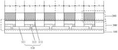
本发明实施例提供的一种阵列基板,如图1a和图1b所示,包括衬底基板100,设置在衬底基板100上且呈矩阵排列的多个像素单元200,以及为各像素单元200提供显示信号的驱动模块(图1a和图1b中未示出驱动模块的结构,);每个像素单元200均分为透光区域a和遮光区域b,还包括:An array substrate provided by an embodiment of the present invention, as shown in FIGS. A drive module that provides display signals (the structure of the drive module is not shown in Figures 1a and 1b); each
与驱动模块电连接的光伏电池组件300,光伏电池组件300如图1a所示设置在衬底基板100与像素单元200之间,或如图1b所示设置在衬底基板100背离像素单元200一侧;A
光伏电池组件300包括多个光伏子电池310,每个光伏子电池310均包括依次层叠设置的第一透明电极311,光伏薄膜312和第二透明电极313;其中,The
光伏薄膜312在衬底基板100的正投影位于遮光区域b内。The orthographic projection of the
本发明实施例提供的上述阵列基板,由于设置了与驱动模块电连接的光伏电池组件,该阵列基板可以利用光伏电池组件将遮光区域的光能转化为电能,并将电能输出到驱动模块供其使用,从而可以有效的利用遮光区域的光能,提高阵列基板对光能的利用率。并且,光伏电池组件中不透光的光伏薄膜在衬底基板的正投影位于遮光区域内,因此,不会影响阵列基板中各像素单元的开口率。The above-mentioned array substrate provided by the embodiment of the present invention is provided with a photovoltaic cell assembly electrically connected to the drive module, the array substrate can use the photovoltaic cell assembly to convert the light energy in the shading area into electric energy, and output the electric energy to the drive module for other In this way, the light energy in the light-shielding area can be effectively utilized, and the utilization rate of the light energy of the array substrate can be improved. Moreover, the orthographic projection of the opaque photovoltaic thin film on the base substrate in the photovoltaic cell module is located in the light-shielding area, so the aperture ratio of each pixel unit in the array substrate will not be affected.
需要说明的是本发明实施例提供的光伏电池组件中的光伏薄膜可以为单结非晶硅薄膜、双结非晶硅薄膜、双结微晶硅薄膜或多结叠层薄膜,或者,也可以是单晶硅薄膜或多晶硅薄膜等,当然,只要是能够实现本发明方案的光伏薄膜,都在本发明的保护范围之内。It should be noted that the photovoltaic film in the photovoltaic cell module provided by the embodiment of the present invention can be a single-junction amorphous silicon film, a double-junction amorphous silicon film, a double-junction microcrystalline silicon film or a multi-junction stacked film, or it can also be It is a monocrystalline silicon thin film or a polycrystalline silicon thin film, etc. Of course, as long as it is a photovoltaic thin film that can realize the solution of the present invention, it is within the protection scope of the present invention.
较佳地,在本发明实施例提供的上述阵列基板中,如图5a和图5b所示,光伏薄膜312可以包括层叠设置的非晶硅薄膜3121和微晶硅薄膜3122,在此不做限定。Preferably, in the above-mentioned array substrate provided by the embodiment of the present invention, as shown in FIG. 5a and FIG. 5b, the
进一步地,在具体实施时,在本发明实施例提供的上述阵列基板中,非晶硅薄膜的厚度控制在200nm~300nm之间为佳,微晶硅薄膜的厚度控制在1μm~3μm之间为佳,在此不做限定。Furthermore, in specific implementation, in the above-mentioned array substrate provided by the embodiment of the present invention, it is better to control the thickness of the amorphous silicon thin film between 200nm and 300nm, and control the thickness of the microcrystalline silicon thin film between 1 μm and 3 μm. Good, no limitation here.
进一步地,在本发明实施例提供的上述阵列基板中,第一透明电极和第二透明电极的材料可以为透明导电氧化物(TCO)材料,当然也可以为能够实现本发明方案的其它材料,在此不做限定。Furthermore, in the above-mentioned array substrate provided by the embodiment of the present invention, the material of the first transparent electrode and the second transparent electrode may be a transparent conductive oxide (TCO) material, of course, it may also be other materials that can realize the solution of the present invention, It is not limited here.
进一步地,在本发明实施例提供的上述阵列基板中,如图1a和图1b所示,第一透明电极311邻近衬底基板100,第二透明电极313远离衬底基板100,在具体实施时,第一透明电极311的厚度控制在1500nm~1800nm之间为佳,第二透明电极313的厚度控制在100nm左右为佳。Further, in the above-mentioned array substrate provided by the embodiment of the present invention, as shown in FIG. 1a and FIG. 1b, the first
较佳地,为了提高光伏电池组件输出的电能的电压,在本发明实施例提供的上述阵列基板中,如图2a和图2b所示,光伏电池组件300可以为串联结构,即多个光伏子电池310之间相互串联,其中,图2a和图2b分别为光伏电池组件300与驱动模块400电连接的平面结构示意图。Preferably, in order to increase the voltage of the electric energy output by the photovoltaic cell assembly, in the above array substrate provided by the embodiment of the present invention, as shown in Figure 2a and Figure 2b, the
较佳地,在本发明实施例提供的上述阵列基板中,相邻的光伏子电池310之间连接最佳,在具体实施时,如图2a所示,相邻的光伏子电池310之间连接可以是同行的相邻光伏子电池310之间连接,相邻两行之间光伏子电池310之间串联通过将位于该相邻两行的同一个端的两个光伏子电池310连接在一起实现;当然,如图2b所示,相邻的光伏子电池310之间连接可以是同列的相邻光伏子电池310之间连接,相邻两列之间光伏子电池310之间串联通过将位于该相邻两列的同一个端的两个光伏子电池310连接在一起实现,当然,各光伏子电池310还可以是通过其他连接方式串联,在此不做限定。Preferably, in the above-mentioned array substrate provided by the embodiment of the present invention, the connection between adjacent
进一步地,在本发明实施例提供的上述阵列基板中,如图3所示,在串联的各个光伏子电池310中,在同一个光伏子电池310中,第一透明电极311与第二透明电极313之间不存在短路现象,且相邻光伏子电池310中的第一透明电极311之间,以及第二透明电极313之间均不存在短路现象。Further, in the above-mentioned array substrate provided by the embodiment of the present invention, as shown in FIG. There is no short circuit between 313 , and there is no short circuit between the first
具体地,在本发明实施例提供的上述阵列基板中,相邻的两个光伏子电池310之间串联的剖面图如图3所示,其中图3为图2a沿A-A’方向的剖面图,在相邻的两个光伏子电池310中,其中一个光伏子电池310的第一透明电极通过贯穿该光伏子电池310的光伏薄膜312的过孔与另一个光伏子电池310的第二透明电极电性313连接,从而实现相邻两个光伏子电池310之间的串联。Specifically, in the above-mentioned array substrate provided by the embodiment of the present invention, the cross-sectional view of the series connection between two adjacent
当然,在本发明实施例提供的上述阵列基板中,为了简化制备工艺,光伏电池组件300也可以为并联结构,即多个该光伏子电池310之间可以相互并联,如图4所示,将各光伏子电池310的第一透明电极311直接连接,即第一透明电极的薄膜直接覆盖整个衬底基板,不需要形成单独的每个第一透明电极311的图形,从而简化制备工艺;同理将各光伏子电池的第二透明电极313直接连接,即第二透明电极的薄膜直接覆盖整个衬底基板,不需要形成单独的每个第二透明电极313的图形,但是该并联结构的光伏电池组件300输出的电压值较低。Of course, in the above-mentioned array substrate provided by the embodiment of the present invention, in order to simplify the manufacturing process, the
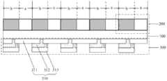
较佳地,为了有效利用遮光区的光能,本发明实施例提供的上述阵列基板,如图5a和图5b所示,还包括:Preferably, in order to effectively utilize the light energy in the shading area, the above-mentioned array substrate provided by the embodiment of the present invention, as shown in Figure 5a and Figure 5b, further includes:
位于像素单元200与光伏电池组件300之间的金属反射层500;A metal
金属反射层500在衬底基板100上的正投影覆盖光伏薄膜312在衬底基板100的正投影,且位于遮光区域内。当然,在具体实施时,也可以不用单独设置金属反射层,直接利用像素单元的遮光区域中的不透明金属信号线或者是薄膜晶体管中的栅极的金属反射作用,来达到设置金属反射层的作用,但是这样,对光能的利用率相比单独设置有金属反射层的阵列基板对光能的利用率相对较低。The orthographic projection of the metal
具体地,在本发明实施例提供的上述阵列基板中,如图5a所示,当像素单元200与光伏电池组件300位于衬底基板100的同一侧时,金属反射层500位于像素单元200与光伏电池组件300之间;当像素单元200与光伏电池组件300分别位于衬底基板100的两侧时,如图5b所示,金属反射层500可以位于衬底基板100与光伏电池组件400之间,或者,金属反射层500也可以位于衬底基板100与像素单元200之间。Specifically, in the above-mentioned array substrate provided by the embodiment of the present invention, as shown in FIG. Between the
较佳地,在本发明实施例提供的上述阵列基板中,如图5a所示,像素单元200与光伏电池组件300位于衬底基板100的同一侧,金属反射层500可以直接位于第二透明电极313之上,第二透明电极313与金属反射层500的图形可以设置为一致。这样在制作时,第二透明电极313与金属反射层500可以通过一次构图工艺形成,从而可以简化制作工艺。Preferably, in the above-mentioned array substrate provided by the embodiment of the present invention, as shown in FIG. 5a, the
或者,较佳地,在本发明实施例提供的上述阵列基板中,如图5b所示,像素单元200与光伏电池组件300分别位于衬底基板100的两侧,金属反射层500可以直接位于第一透明电极311之上,第一透明电极311与金属反射层500的图形可以设置为一致。这样在制作时,第一透明电极311与金属反射层500可以通过一次构图工艺形成,从而可以简化制作工艺。Or, preferably, in the above-mentioned array substrate provided by the embodiment of the present invention, as shown in FIG. On a
进一步地,在具体实施时,在本发明实施例提供的上述阵列基板中,金属反射层的材料优选铝或银,当然,金属反射层的材料也可以为能够实现本发明方案的其他材料,在此不做限定。Furthermore, in specific implementation, in the above-mentioned array substrate provided by the embodiment of the present invention, the material of the metal reflective layer is preferably aluminum or silver. Of course, the material of the metal reflective layer can also be other materials that can realize the solution of the present invention. This is not limited.
较佳地,在本发明实施例提供的上述阵列基板中,如图5a所示,像素单元200与光伏电池组件300位于衬底基板100的同一侧,为了避免像素单元200在制备过程中由于光伏电池组件表面高度不一致而导致的段差,还包括:Preferably, in the above-mentioned array substrate provided by the embodiment of the present invention, as shown in FIG. The level difference caused by the inconsistent surface height of battery components also includes:
位于光伏电池组件300和像素单元200之间的平坦化层600。The
较佳地,在本发明实施例提供的上述阵列基板中,平坦化层可以包括依次层叠设置的氮化硅薄膜、树脂薄膜和氮化硅薄膜;或者,平坦化层也可以包括依次层叠设置的二氧化硅薄膜、树脂薄膜和二氧化硅薄膜,其中树脂薄膜采用耐高温的树脂材料制备,在此不做限定。Preferably, in the above-mentioned array substrate provided by the embodiment of the present invention, the planarization layer may include a silicon nitride film, a resin film, and a silicon nitride film that are sequentially stacked; or, the planarization layer may also include sequentially stacked Silicon dioxide film, resin film and silicon dioxide film, wherein the resin film is made of high temperature resistant resin material, which is not limited here.
较佳地,在本发明实施例提供的上述阵列基板中,在像素单元与光伏电池组件分别位于衬底基板的两侧时,为了保护光伏电池组件,还需要在光伏电池组件背离衬底基板的最外侧设置透明保护层,在此不做赘述。Preferably, in the above-mentioned array substrate provided by the embodiment of the present invention, when the pixel unit and the photovoltaic cell assembly are respectively located on both sides of the base substrate, in order to protect the photovoltaic cell assembly, it is also necessary to place the photovoltaic cell assembly away from the base substrate A transparent protective layer is provided on the outermost side, which will not be described in detail here.
较佳地,为了使光伏电池组件所转化的电能可以稳定的输送给驱动模块,在本发明实施例提供的上述阵列基板中,如图2a和图2b所示,还可以包括:稳压稳流模块700,光伏电池组件300通过稳压稳流模块700与驱动模块400电连接。Preferably, in order to ensure that the electric energy converted by the photovoltaic cell module can be stably delivered to the drive module, in the above-mentioned array substrate provided by the embodiment of the present invention, as shown in Fig. 2a and Fig. 2b, it may further include: voltage and
下面以图5a所示的阵列基板为例,对上述阵列基板的制备方法进行说明。Hereinafter, taking the array substrate shown in FIG. 5a as an example, the method for preparing the above-mentioned array substrate will be described.
具体地,制备图5a所示的阵列基板,具体制作过程包括以下几个步骤:Specifically, the array substrate shown in Figure 5a is prepared, and the specific manufacturing process includes the following steps:
(1)在衬底基板100上形成第一透明电极311的图形,如图6a所示;(1) forming a pattern of the first
具体地,在具体实施时:首先,通过脉冲激光沉积、金属有机物化学气相沉积、射频/中频/直流溅射、电子束和热反应蒸发、喷雾热分解、溶胶-凝胶法、等离子体化学气相沉积等方法在衬底基板上沉积第一透明导电氧化物薄膜TCO;较佳地,第一透明导电氧化物薄膜的厚度控制在1500nm~1800nm之间为佳;Specifically, in the specific implementation: first, through pulsed laser deposition, metal organic chemical vapor deposition, radio frequency/intermediate frequency/DC sputtering, electron beam and thermal reaction evaporation, spray pyrolysis, sol-gel method, plasma chemical vapor phase Deposit the first transparent conductive oxide film TCO on the base substrate by methods such as deposition; preferably, the thickness of the first transparent conductive oxide film is preferably controlled between 1500nm and 1800nm;
接着,通过CH3COOH对第一透明导电氧化物薄膜表面进行湿法刻蚀处理,使该第一透明导电氧化物薄膜表面具有绒面结构;具体地,CH3COOH浓度控制在0.5%左右,湿法刻蚀处理时间控制在20分至30分之间为佳;Next, wet-etching the surface of the first transparent conductive oxide film with CH3 COOH, so that the surface of the first transparent conductive oxide film has a textured structure; specifically, the concentration of CH3 COOH is controlled at about 0.5%, It is better to control the wet etching treatment time between 20 minutes and 30 minutes;
最后,通过激光切割或湿法刻蚀的方法在该具有绒面结构的第一透明导电氧化物薄膜中形成第一透明电极的图形。Finally, a pattern of the first transparent electrode is formed in the first transparent conductive oxide film with a textured structure by laser cutting or wet etching.
(2)在第一透明电极311上形成光伏薄膜312的图形,如图6b所示;(2) forming a pattern of a
具体地,在具体实施时:首先,通过化学气相沉积方法在第一透明电极上依次沉积非晶硅薄膜和微晶硅薄膜;较佳地,非晶硅薄膜的厚度控制在200nm~300nm之间,微晶硅薄膜的厚度控制在1μm~3μm之间为佳;Specifically, during specific implementation: first, an amorphous silicon film and a microcrystalline silicon film are sequentially deposited on the first transparent electrode by chemical vapor deposition; preferably, the thickness of the amorphous silicon film is controlled between 200nm and 300nm , the thickness of the microcrystalline silicon film is preferably controlled between 1 μm and 3 μm;
然后,通过激光切割或干法刻蚀的方法在该非晶硅薄膜和微晶硅薄膜中形成光伏薄膜的图形。Then, a photovoltaic thin film pattern is formed in the amorphous silicon thin film and the microcrystalline silicon thin film by means of laser cutting or dry etching.
(3)通过一次构图工艺在光伏薄膜312上同时形成第二透明电极313和金属反射层500的图形,如图6c所示;(3) Simultaneously form the pattern of the second
具体地,在具体实施时:首先,在微晶硅薄膜3122上沉积第二透明导电氧化物薄膜TCO;较佳地,第二透明导电氧化物薄膜的厚度控制在100nm左右为佳;Specifically, during implementation: first, deposit a second transparent conductive oxide film TCO on the
接着,通过物理气相沉积的方法在第二透明导电氧化物薄膜上沉积反射金属薄膜;较佳地,反射金属薄膜的材料为银或铝;Next, deposit a reflective metal film on the second transparent conductive oxide film by physical vapor deposition; preferably, the material of the reflective metal film is silver or aluminum;
最后,通过一次构图工艺在第二透明导电氧化物薄膜和反射金属薄膜中形成第二透明电极和金属反射层的图形;具体地,构图工艺可以为激光切割或湿法刻蚀。Finally, patterns of the second transparent electrode and the metal reflective layer are formed in the second transparent conductive oxide film and the reflective metal film through a patterning process; specifically, the patterning process can be laser cutting or wet etching.
(4)在金属反射层500上沉积平坦化层600,如图6d所示;(4) Depositing a
具体地,在具体实施时,平坦化层的材料优选为氮化硅(SiNx)/树脂材料(Resin)/氮化硅(SiNx)或二氧化硅(SiO2)/树脂材料(Resin)/二氧化硅(SiO2),其中树脂材料采用耐高温的树脂材料;进一步地,氮化硅或二氧化硅薄膜可以采用化学气相沉积的方法沉积,树脂材料可以采用旋涂工艺制备。Specifically, in specific implementation, the material of the planarization layer is preferably silicon nitride (SiNx)/resin material (Resin)/silicon nitride (SiNx) or silicon dioxide (SiO2)/resin material (Resin)/dioxide Silicon (SiO2), wherein the resin material is a high temperature resistant resin material; further, silicon nitride or silicon dioxide film can be deposited by chemical vapor deposition, and the resin material can be prepared by spin coating process.
(5)在平坦化层600上形成像素单元200的图形,如图5a所示。(5) Forming the pattern of the
具体地,像素单元的图形的制作与现有技术一致,在此不再赘述。具体地,经过上述步骤(1)至(5)之后,得到本发明实施例图5a所示的阵列基板。Specifically, the making of the graphic of the pixel unit is consistent with the prior art, and will not be repeated here. Specifically, after the above steps (1) to (5), the array substrate shown in FIG. 5 a of the embodiment of the present invention is obtained.
需要说明的是,本发明实施例提供的上述阵列基板可以应用于液晶显示面板中,也可以应用于有机电致发光显示器件中,在此不做限定。It should be noted that the above-mentioned array substrate provided by the embodiment of the present invention can be applied to a liquid crystal display panel, or can also be applied to an organic electroluminescent display device, which is not limited here.
具体地,当本发明实施例提供的上述阵列基板应用于液晶显示面板中时,在本发明实施例提供的上述阵列基板中,像素单元包括位于遮光区域内的薄膜晶体管和金属信号线,以及位于透光区域的像素电极,具体地,阵列基板中的像素单元为现有技术,在此不再赘述。Specifically, when the above-mentioned array substrate provided by the embodiment of the present invention is applied to a liquid crystal display panel, in the above-mentioned array substrate provided by the embodiment of the present invention, the pixel unit includes a thin film transistor and a metal signal line located in the light-shielding area, and a The pixel electrodes in the light-transmitting region, specifically, the pixel units in the array substrate are prior art, and will not be repeated here.
基于同一发明构思,本发明实施例还提供了一种液晶显示面板,包括本发明实施例提供的上述阵列基板,由于该液晶显示面板解决问题的原理与前述一种阵列基板相似,因此该液晶显示面板的实施可以参见前述阵列基板的实施,重复之处不再赘述。Based on the same inventive concept, an embodiment of the present invention also provides a liquid crystal display panel, including the above-mentioned array substrate provided by the embodiment of the present invention. Since the problem-solving principle of the liquid crystal display panel is similar to that of the aforementioned array substrate, the liquid crystal display For the implementation of the panel, reference may be made to the implementation of the aforementioned array substrate, and repeated descriptions will not be repeated.
基于同一发明构思,本发明实施例还提供了一种显示装置,包括本发明实施例提供的上述液晶显示面板,该显示装置可以为:手机、平板电脑、电视机、显示器、笔记本电脑、数码相框、导航仪等任何具有显示功能的产品或部件。对于该显示装置的其它必不可少的组成部分均为本领域的普通技术人员应该理解具有的,在此不做赘述,也不应作为对本发明的限制。该显示装置的实施可以参见上述液晶显示面板的实施例,重复之处不再赘述。Based on the same inventive concept, an embodiment of the present invention also provides a display device, including the above-mentioned liquid crystal display panel provided by the embodiment of the present invention, and the display device can be: a mobile phone, a tablet computer, a TV set, a monitor, a notebook computer, a digital photo frame , navigator and any other product or component with display function. The other essential components of the display device should be understood by those of ordinary skill in the art, and will not be repeated here, nor should they be regarded as limitations on the present invention. For the implementation of the display device, reference may be made to the above-mentioned embodiments of the liquid crystal display panel, and repeated descriptions will not be repeated.
本发明实施例提供的一种阵列基板、液晶显示面板及显示装置,该阵列基板包括衬底基板,设置在衬底基板上且呈矩阵排列的多个像素单元,以及为各像素单元提供显示信号的驱动模块;每个像素单元均分为透光区域和遮光区域,还包括:与驱动模块电连接的光伏电池组件,光伏电池组件设置在衬底基板与像素单元之间,或设置在衬底基板背离像素单元一侧;光伏电池组件包括多个光伏子电池,每个光伏子电池均包括依次层叠设置的第一透明电极,光伏薄膜和第二透明电极;其中,光伏薄膜在衬底基板的正投影位于所述遮光区域内。本发明实施例提供的上述阵列基板,由于设置了与驱动模块电连接的光伏电池组件,该阵列基板可以利用光伏电池组件将遮光区域的光能转化为电能,并将电能输出到驱动模块供其使用,从而可以有效的利用遮光区域的光能,提高阵列基板对光能的利用率。并且,光伏电池组件中不透光的光伏薄膜在衬底基板的正投影位于遮光区域内,因此,不会影响阵列基板中各像素单元的开口率。An array substrate, a liquid crystal display panel, and a display device provided by an embodiment of the present invention, the array substrate includes a base substrate, a plurality of pixel units disposed on the base substrate and arranged in a matrix, and providing display signals for each pixel unit drive module; each pixel unit is divided into a light-transmitting area and a light-shielding area, and also includes: a photovoltaic cell assembly electrically connected to the drive module, and the photovoltaic cell assembly is arranged between the substrate substrate and the pixel unit, or arranged on the substrate The substrate is away from the side of the pixel unit; the photovoltaic cell assembly includes a plurality of photovoltaic sub-cells, and each photovoltaic sub-cell includes a first transparent electrode, a photovoltaic film and a second transparent electrode stacked in sequence; wherein, the photovoltaic film is on the base substrate The orthographic projection is located within the shading area. The above-mentioned array substrate provided by the embodiment of the present invention is provided with a photovoltaic cell assembly electrically connected to the drive module, the array substrate can use the photovoltaic cell assembly to convert the light energy in the shading area into electric energy, and output the electric energy to the drive module for other In this way, the light energy in the light-shielding area can be effectively utilized, and the utilization rate of the light energy of the array substrate can be improved. Moreover, the orthographic projection of the opaque photovoltaic thin film on the base substrate in the photovoltaic cell module is located in the light-shielding area, so the aperture ratio of each pixel unit in the array substrate will not be affected.
显然,本领域的技术人员可以对本发明进行各种改动和变型而不脱离本发明的精神和范围。这样,倘若本发明的这些修改和变型属于本发明权利要求及其等同技术的范围之内,则本发明也意图包含这些改动和变型在内。Obviously, those skilled in the art can make various changes and modifications to the present invention without departing from the spirit and scope of the present invention. Thus, if these modifications and variations of the present invention fall within the scope of the claims of the present invention and their equivalent technologies, the present invention also intends to include these modifications and variations.
Claims (10)
Translated fromChinesePriority Applications (3)
| Application Number | Priority Date | Filing Date | Title |
|---|---|---|---|
| CN201410010209.6ACN103760707A (en) | 2014-01-09 | 2014-01-09 | Array substrate, liquid crystal display panel and display device |
| PCT/CN2014/081985WO2015103859A1 (en) | 2014-01-09 | 2014-07-10 | Array substrate, liquid crystal display panel and display device |
| US14/428,932US9348161B2 (en) | 2014-01-09 | 2014-07-10 | Array substrate, liquid crystal display panel and display device |
Applications Claiming Priority (1)
| Application Number | Priority Date | Filing Date | Title |
|---|---|---|---|
| CN201410010209.6ACN103760707A (en) | 2014-01-09 | 2014-01-09 | Array substrate, liquid crystal display panel and display device |
Publications (1)
| Publication Number | Publication Date |
|---|---|
| CN103760707Atrue CN103760707A (en) | 2014-04-30 |
Family
ID=50527966
Family Applications (1)
| Application Number | Title | Priority Date | Filing Date |
|---|---|---|---|
| CN201410010209.6APendingCN103760707A (en) | 2014-01-09 | 2014-01-09 | Array substrate, liquid crystal display panel and display device |
Country Status (3)
| Country | Link |
|---|---|
| US (1) | US9348161B2 (en) |
| CN (1) | CN103760707A (en) |
| WO (1) | WO2015103859A1 (en) |
Cited By (14)
| Publication number | Priority date | Publication date | Assignee | Title |
|---|---|---|---|---|
| CN103680328A (en)* | 2013-12-31 | 2014-03-26 | 京东方科技集团股份有限公司 | Array substrate and display device |
| WO2015103859A1 (en)* | 2014-01-09 | 2015-07-16 | 京东方科技集团股份有限公司 | Array substrate, liquid crystal display panel and display device |
| CN106292015A (en)* | 2015-05-12 | 2017-01-04 | 北京铂阳顶荣光伏科技有限公司 | A kind of photovoltaic display device |
| CN106597721A (en)* | 2016-12-05 | 2017-04-26 | Tcl集团股份有限公司 | Display panel, display device and manufacturing method of display panel |
| CN108169966A (en)* | 2018-01-04 | 2018-06-15 | 京东方科技集团股份有限公司 | Drop control detector part and drop control detection method |
| CN110147007A (en)* | 2019-05-30 | 2019-08-20 | 重庆蓝岸通讯技术有限公司 | Energy recovery structure of LTPS display panel based on photovoltaic effect |
| CN110890411A (en)* | 2019-11-29 | 2020-03-17 | 京东方科技集团股份有限公司 | A display panel and display device |
| CN111652196A (en)* | 2020-07-17 | 2020-09-11 | 厦门天马微电子有限公司 | Display panel and display device |
| WO2020237697A1 (en)* | 2019-05-31 | 2020-12-03 | 信利半导体有限公司 | Thin film photovoltaic cell series structure and preparation process for thin film photovoltaic cell series connection |
| WO2020252808A1 (en)* | 2019-06-21 | 2020-12-24 | 信利半导体有限公司 | Thin-film photovoltaic cell and manufacturing method therefor |
| WO2021139332A1 (en)* | 2020-01-08 | 2021-07-15 | 信利半导体有限公司 | Display module having integrated thin film solar cell, and manufacturing method therefor |
| CN113568203A (en)* | 2020-04-28 | 2021-10-29 | 群创光电股份有限公司 | LCD device and sunglasses |
| CN115951529A (en)* | 2022-12-29 | 2023-04-11 | Tcl华星光电技术有限公司 | Glass device, light-adjusting glass and display device |
| CN116520598A (en)* | 2022-01-20 | 2023-08-01 | 虹彩光电股份有限公司 | Cholesteric liquid crystal display device |
Families Citing this family (5)
| Publication number | Priority date | Publication date | Assignee | Title |
|---|---|---|---|---|
| CN105826328B (en)* | 2016-05-03 | 2019-03-05 | 京东方科技集团股份有限公司 | Array substrate and its manufacturing method, display device |
| CN107065328A (en)* | 2017-05-23 | 2017-08-18 | 京东方科技集团股份有限公司 | A kind of dot structure, display panel, display device and pixel structure preparation method |
| CN107393981B (en)* | 2017-09-13 | 2023-08-15 | 李会欣 | Deep back electrode photovoltaic cell assembly, processing method and photovoltaic system |
| US11841686B2 (en)* | 2020-11-09 | 2023-12-12 | Garmin Switzerland Gmbh | Integrated energy-collecting display module with core out |
| TWI796102B (en)* | 2022-01-20 | 2023-03-11 | 虹彩光電股份有限公司 | Cholesterol liquid crystal display device |
Citations (8)
| Publication number | Priority date | Publication date | Assignee | Title |
|---|---|---|---|---|
| CN101813849A (en)* | 2009-02-19 | 2010-08-25 | 北京京东方光电科技有限公司 | Colored film substrate, manufacturing method thereof and liquid crystal display panel |
| CN101828145A (en)* | 2007-10-19 | 2010-09-08 | 高通Mems科技公司 | Display with integrated photovoltaics |
| CN101989636A (en)* | 2009-08-06 | 2011-03-23 | 三星电子株式会社 | Solar cell module and method of manufacturing the same |
| CN101995691A (en)* | 2009-08-20 | 2011-03-30 | 上海天马微电子有限公司 | Liquid crystal display device having a plurality of pixel electrodes |
| US20110249219A1 (en)* | 2010-04-13 | 2011-10-13 | Allan Evans | Integrated display and photovoltaic element |
| CN102751242A (en)* | 2012-07-27 | 2012-10-24 | 深圳市华星光电技术有限公司 | Method for fabricating array substrate having embedded photovoltaic cell and array substrate fabricated by method |
| CN103258841A (en)* | 2013-04-26 | 2013-08-21 | 京东方科技集团股份有限公司 | Display panel, display device and electronic device |
| CN103474452A (en)* | 2013-09-13 | 2013-12-25 | 北京京东方光电科技有限公司 | Display panel and manufacturing method and terminal equipment thereof |
Family Cites Families (6)
| Publication number | Priority date | Publication date | Assignee | Title |
|---|---|---|---|---|
| JP4044187B2 (en)* | 1997-10-20 | 2008-02-06 | 株式会社半導体エネルギー研究所 | Active matrix display device and manufacturing method thereof |
| US7242449B1 (en)* | 1999-07-23 | 2007-07-10 | Semiconductor Energy Laboratory Co., Ltd. | Semiconductor device and integral image recognition/display apparatus |
| JP2010034512A (en)* | 2008-07-01 | 2010-02-12 | Fujifilm Corp | Solid-state imaging element and imaging device |
| JP5560142B2 (en)* | 2010-02-10 | 2014-07-23 | 富士フイルム株式会社 | Photoelectric conversion device and solid-state imaging device |
| JP4783861B1 (en)* | 2010-02-25 | 2011-09-28 | 富士フイルム株式会社 | Imaging device, manufacturing method of imaging device, and imaging apparatus |
| CN103760707A (en)* | 2014-01-09 | 2014-04-30 | 北京京东方光电科技有限公司 | Array substrate, liquid crystal display panel and display device |
- 2014
- 2014-01-09CNCN201410010209.6Apatent/CN103760707A/enactivePending
- 2014-07-10USUS14/428,932patent/US9348161B2/ennot_activeExpired - Fee Related
- 2014-07-10WOPCT/CN2014/081985patent/WO2015103859A1/enactiveApplication Filing
Patent Citations (8)
| Publication number | Priority date | Publication date | Assignee | Title |
|---|---|---|---|---|
| CN101828145A (en)* | 2007-10-19 | 2010-09-08 | 高通Mems科技公司 | Display with integrated photovoltaics |
| CN101813849A (en)* | 2009-02-19 | 2010-08-25 | 北京京东方光电科技有限公司 | Colored film substrate, manufacturing method thereof and liquid crystal display panel |
| CN101989636A (en)* | 2009-08-06 | 2011-03-23 | 三星电子株式会社 | Solar cell module and method of manufacturing the same |
| CN101995691A (en)* | 2009-08-20 | 2011-03-30 | 上海天马微电子有限公司 | Liquid crystal display device having a plurality of pixel electrodes |
| US20110249219A1 (en)* | 2010-04-13 | 2011-10-13 | Allan Evans | Integrated display and photovoltaic element |
| CN102751242A (en)* | 2012-07-27 | 2012-10-24 | 深圳市华星光电技术有限公司 | Method for fabricating array substrate having embedded photovoltaic cell and array substrate fabricated by method |
| CN103258841A (en)* | 2013-04-26 | 2013-08-21 | 京东方科技集团股份有限公司 | Display panel, display device and electronic device |
| CN103474452A (en)* | 2013-09-13 | 2013-12-25 | 北京京东方光电科技有限公司 | Display panel and manufacturing method and terminal equipment thereof |
Cited By (20)
| Publication number | Priority date | Publication date | Assignee | Title |
|---|---|---|---|---|
| CN103680328A (en)* | 2013-12-31 | 2014-03-26 | 京东方科技集团股份有限公司 | Array substrate and display device |
| CN103680328B (en)* | 2013-12-31 | 2015-09-09 | 京东方科技集团股份有限公司 | Array substrate and display device |
| US9559126B2 (en) | 2013-12-31 | 2017-01-31 | Boe Technology Group Co., Ltd. | Array substrate and display device |
| WO2015103859A1 (en)* | 2014-01-09 | 2015-07-16 | 京东方科技集团股份有限公司 | Array substrate, liquid crystal display panel and display device |
| US9348161B2 (en) | 2014-01-09 | 2016-05-24 | Boe Technology Group Co., Ltd. | Array substrate, liquid crystal display panel and display device |
| CN106292015A (en)* | 2015-05-12 | 2017-01-04 | 北京铂阳顶荣光伏科技有限公司 | A kind of photovoltaic display device |
| CN106597721A (en)* | 2016-12-05 | 2017-04-26 | Tcl集团股份有限公司 | Display panel, display device and manufacturing method of display panel |
| CN106597721B (en)* | 2016-12-05 | 2020-10-27 | Tcl科技集团股份有限公司 | Display panel, display device and manufacturing method of display panel |
| CN108169966B (en)* | 2018-01-04 | 2020-08-18 | 京东方科技集团股份有限公司 | Droplet control detection device and droplet control detection method |
| CN108169966A (en)* | 2018-01-04 | 2018-06-15 | 京东方科技集团股份有限公司 | Drop control detector part and drop control detection method |
| CN110147007A (en)* | 2019-05-30 | 2019-08-20 | 重庆蓝岸通讯技术有限公司 | Energy recovery structure of LTPS display panel based on photovoltaic effect |
| WO2020237697A1 (en)* | 2019-05-31 | 2020-12-03 | 信利半导体有限公司 | Thin film photovoltaic cell series structure and preparation process for thin film photovoltaic cell series connection |
| WO2020252808A1 (en)* | 2019-06-21 | 2020-12-24 | 信利半导体有限公司 | Thin-film photovoltaic cell and manufacturing method therefor |
| CN110890411A (en)* | 2019-11-29 | 2020-03-17 | 京东方科技集团股份有限公司 | A display panel and display device |
| WO2021139332A1 (en)* | 2020-01-08 | 2021-07-15 | 信利半导体有限公司 | Display module having integrated thin film solar cell, and manufacturing method therefor |
| CN113568203A (en)* | 2020-04-28 | 2021-10-29 | 群创光电股份有限公司 | LCD device and sunglasses |
| CN111652196A (en)* | 2020-07-17 | 2020-09-11 | 厦门天马微电子有限公司 | Display panel and display device |
| CN111652196B (en)* | 2020-07-17 | 2022-12-09 | 厦门天马微电子有限公司 | Display panel and display device |
| CN116520598A (en)* | 2022-01-20 | 2023-08-01 | 虹彩光电股份有限公司 | Cholesteric liquid crystal display device |
| CN115951529A (en)* | 2022-12-29 | 2023-04-11 | Tcl华星光电技术有限公司 | Glass device, light-adjusting glass and display device |
Also Published As
| Publication number | Publication date |
|---|---|
| US20160041414A1 (en) | 2016-02-11 |
| WO2015103859A1 (en) | 2015-07-16 |
| US9348161B2 (en) | 2016-05-24 |
Similar Documents
| Publication | Publication Date | Title |
|---|---|---|
| CN103760707A (en) | Array substrate, liquid crystal display panel and display device | |
| US8194197B2 (en) | Integrated display and photovoltaic element | |
| CN104022077B (en) | Array substrate, preparing method thereof and display device | |
| US20200258954A1 (en) | Display Panel, Method for Manufacturing the Same, and Display Device | |
| CN102725857A (en) | Solar cell, solar cell module using solar cell, and manufacturing method for solar cell | |
| WO2015100898A1 (en) | Thin-film transistor, tft array substrate and manufacturing method therefor, and display device | |
| CN104091761B (en) | Patterned film preparation method, display substrate and display device | |
| CN102253547B (en) | Array substrate and manufacturing method thereof as well as liquid crystal display | |
| KR20090076572A (en) | Display substrate, electrophoretic display device including same, manufacturing method of display substrate | |
| US20210408304A1 (en) | Thin-film photovoltaic cell with high photoelectric conversion rate and preparation process thereof | |
| KR20090005872A (en) | Solar cell and manufacturing method thereof | |
| CN108447919A (en) | Preparation method of thin film solar cell module | |
| CN114047651B (en) | Spatial light modulator and method for manufacturing the same | |
| CN110277473B (en) | Manufacturing method of thin film photovoltaic cell and thin film photovoltaic cell | |
| CN103943631A (en) | Thin film transistor array substrate, preparation method thereof and liquid crystal display | |
| CN103676361A (en) | Display screen, manufacturing method of display screen, and display device | |
| CN101546786A (en) | Thin film type solar cell, and method for manufacturing the same | |
| JPH0851229A (en) | Integrated solar battery and its manufacture | |
| US9087953B2 (en) | Solar cell module and method for manufacturing the same | |
| CN103941448A (en) | Thin film transistor array substrate, preparation method thereof and liquid crystal display | |
| US20110030769A1 (en) | Solar cell and method for manufacturing the same | |
| CN111081152A (en) | A display module integrating thin-film solar cells and preparation method thereof | |
| CN102902123B (en) | Solar liquid crystal panel and manufacturing method thereof | |
| CN211150572U (en) | Thin film solar cell | |
| CN107123694A (en) | A kind of light transmission film solar cell module and its manufacture method |
Legal Events
| Date | Code | Title | Description |
|---|---|---|---|
| C06 | Publication | ||
| PB01 | Publication | ||
| C10 | Entry into substantive examination | ||
| SE01 | Entry into force of request for substantive examination | ||
| RJ01 | Rejection of invention patent application after publication | ||
| RJ01 | Rejection of invention patent application after publication | Application publication date:20140430 |