CN103730091A - Pixel compensation circuit - Google Patents
Pixel compensation circuitDownload PDFInfo
- Publication number
- CN103730091A CN103730091ACN201410032056.5ACN201410032056ACN103730091ACN 103730091 ACN103730091 ACN 103730091ACN 201410032056 ACN201410032056 ACN 201410032056ACN 103730091 ACN103730091 ACN 103730091A
- Authority
- CN
- China
- Prior art keywords
- transistor
- signal
- compensation circuit
- terminal
- pixel compensation
- Prior art date
- Legal status (The legal status is an assumption and is not a legal conclusion. Google has not performed a legal analysis and makes no representation as to the accuracy of the status listed.)
- Pending
Links
- 239000010409thin filmSubstances0.000claimsabstractdescription31
- 229920001621AMOLEDPolymers0.000claimsdescription14
- 239000003990capacitorSubstances0.000claimsdescription12
- 238000010586diagramMethods0.000description12
- 238000000034methodMethods0.000description4
- 239000011159matrix materialSubstances0.000description3
- 230000007547defectEffects0.000description2
- 230000000694effectsEffects0.000description2
- 238000006467substitution reactionMethods0.000description2
- 239000008186active pharmaceutical agentSubstances0.000description1
- 239000004973liquid crystal related substanceSubstances0.000description1
- 238000004519manufacturing processMethods0.000description1
- 239000002184metalSubstances0.000description1
Images


Landscapes
- Electroluminescent Light Sources (AREA)
Abstract
Description
Translated fromChinese技术领域technical field
本发明涉及液晶显示技术,尤其涉及一种可补偿薄膜晶体管迁移率漂移的像素补偿电路。The invention relates to liquid crystal display technology, in particular to a pixel compensation circuit capable of compensating the mobility drift of a thin film transistor.
背景技术Background technique
有机发光二极管(Organic Light Emitting Diode,OLED)依驱动方式可分为被动式矩阵驱动(Passive Matrix OLED,PMOLED)和主动式矩阵驱动(Active Matrix OLED,AMOLED)两种。其中,PMOLED是当数据未写入时,发光二极管并不发光;只有在数据写入期间,发光二极管才发光。由于这种驱动方式结构简单,成本较低,容易设计,主要适用于中小尺寸的显示器。Organic light emitting diodes (Organic Light Emitting Diode, OLED) can be divided into passive matrix drive (Passive Matrix OLED, PMOLED) and active matrix drive (Active Matrix OLED, AMOLED) according to the driving method. Among them, PMOLED means that when the data is not written, the light emitting diode does not emit light; only when the data is written, the light emitting diode emits light. Because this driving method is simple in structure, low in cost and easy to design, it is mainly suitable for small and medium-sized displays.
AMOLED与PMOLED最大的差异是在于,每一像素都有一电容存储数据,让每一像素皆维持在发光状态。由于AMOLED耗电量明显小于PMOLED,加上其驱动方式适合发展大尺寸与高解析度的显示器,使得AMOLED成为未来发展的主要方向。在现有技术中,AMOLED的一种像素补偿电路为“2T1C”(两个薄膜晶体管,一个电容)架构。其中,第一薄膜晶体管的源极电性连接至一数据电压,其栅极电性连接至一扫描线,第二薄膜晶体管的栅极电性连接至第一薄膜晶体管的漏极,第二薄膜晶体管的源极电性连接至一第一电压且与栅极之间包括一存储电容,第二薄膜晶体管的漏极连接至一有机发光二极管的阳极,而该有机发光二极管的阴极电性连接至一第二电压。由上述可知,因AMOLED面板上的第一电压于每个像素间都连接在一起,当驱动对应的有机发光二极管发光时,第一电压上会有电流流过。考虑到第一电压的金属线本身具有阻抗,会有压降存在,造成每一像素的第一电压会出现差异,从而导致不同像素间存在电流差异。如此一来,流经有机发光二极管的电流不同,所产生的亮度也不同,进而AMOLED面板不均匀。另外,由于制程的影响,每一像素中的薄膜晶体管的阈值电压均不相同,即使提供相同数值的数据电压,其所产生的电流仍然会有差异,这也将造成面板不均匀。此外,如果采用像素补偿电路对上述电压进行补偿,大部分补偿电路又会受限于扫描时间太短而影响补偿效果。再者,AMOLED中的薄膜晶体管的迁移率(mobility)容易出现漂移,现有的像素补偿电路对其进行补偿时,仅仅只改善部分灰阶范围的迁移率变异,并无法对所有灰阶范围内的迁移率进行补偿,面板不均匀的现象仍然存在。The biggest difference between AMOLED and PMOLED is that each pixel has a capacitor to store data, so that each pixel can maintain a light-emitting state. Since the power consumption of AMOLED is significantly lower than that of PMOLED, and its driving method is suitable for the development of large-size and high-resolution displays, AMOLED will become the main direction of future development. In the prior art, a pixel compensation circuit of AMOLED is a "2T1C" (two thin film transistors, one capacitor) architecture. Wherein, the source of the first thin film transistor is electrically connected to a data voltage, the gate thereof is electrically connected to a scan line, the gate of the second thin film transistor is electrically connected to the drain of the first thin film transistor, and the second thin film transistor is electrically connected to the drain of the first thin film transistor. The source of the transistor is electrically connected to a first voltage and includes a storage capacitor with the gate, the drain of the second thin film transistor is connected to the anode of an organic light emitting diode, and the cathode of the organic light emitting diode is electrically connected to a second voltage. From the above, it can be known that since the first voltage on the AMOLED panel is connected between each pixel, when the corresponding OLED is driven to emit light, a current will flow through the first voltage. Considering that the metal line of the first voltage has impedance itself, there will be a voltage drop, which will cause a difference in the first voltage of each pixel, thereby resulting in a difference in current between different pixels. In this way, different currents flowing through the organic light-emitting diodes will produce different brightness, and thus the AMOLED panel will be uneven. In addition, due to the influence of the manufacturing process, the threshold voltages of the thin film transistors in each pixel are different. Even if the data voltages of the same value are provided, the currents generated by them still vary, which will also cause uneven panel. In addition, if a pixel compensation circuit is used to compensate the above-mentioned voltage, most of the compensation circuits will be limited by the scan time being too short to affect the compensation effect. Furthermore, the mobility of thin-film transistors in AMOLED is prone to drift. When the existing pixel compensation circuit compensates for it, it only improves the mobility variation in some gray-scale ranges, and cannot correct all gray-scale ranges. The mobility is compensated, and the phenomenon of panel unevenness still exists.
有鉴于此,如何设计一种新颖的像素补偿电路或对现有的像素补偿电路进行改进,以有效改善或消除面板不均匀等诸多缺陷,是业内相关技术人员亟待解决的一项课题。In view of this, how to design a novel pixel compensation circuit or improve the existing pixel compensation circuit to effectively improve or eliminate many defects such as panel unevenness is an urgent task for relevant technical personnel in the industry to solve.
发明内容Contents of the invention
针对现有技术中的像素补偿电路在改善面板不均匀时所存在的上述缺陷,本发明提供了一种新颖的、可补偿薄膜晶体管迁移率漂移的像素补偿电路。Aiming at the above-mentioned defects of the pixel compensation circuit in the prior art when improving panel unevenness, the present invention provides a novel pixel compensation circuit capable of compensating the mobility drift of a thin film transistor.
依据本发明的一个方面,提供了一种像素补偿电路,用以补偿薄膜晶体管的迁移率的漂移,该像素补偿电路包括:According to one aspect of the present invention, a pixel compensation circuit is provided for compensating the drift of the mobility of a thin film transistor, the pixel compensation circuit includes:
一第一晶体管,具有一第一端、一第二端和一控制端,所述第一晶体管的控制端用以接收一扫描信号,所述第一晶体管的第一端用以接收一数据信号;A first transistor has a first terminal, a second terminal and a control terminal, the control terminal of the first transistor is used to receive a scan signal, and the first terminal of the first transistor is used to receive a data signal ;
一第二晶体管,具有一第一端、一第二端和一控制端,所述第二晶体管的控制端电性耦接所述第一晶体管的第二端,所述第二晶体管的第二端用以接收一控制信号,所述第二晶体管的第一端与所述第一晶体管的第二端之间还包括一第一电容;以及A second transistor has a first terminal, a second terminal and a control terminal, the control terminal of the second transistor is electrically coupled to the second terminal of the first transistor, and the second terminal of the second transistor The terminal is used to receive a control signal, and a first capacitor is further included between the first terminal of the second transistor and the second terminal of the first transistor; and
一发光二极管,其阳极电性连接至所述第二晶体管的第一端,其阴极电性连接至一接地电压,并且所述发光二极管的阳极与阴极之间还包括一第二电容,其中,在数据写入期间,所述扫描信号的脉冲宽度根据所述数据信号的大小进行调节,以补偿所述薄膜晶体管的迁移率。A light-emitting diode, the anode of which is electrically connected to the first terminal of the second transistor, and the cathode of which is electrically connected to a ground voltage, and a second capacitor is also included between the anode and the cathode of the light-emitting diode, wherein, During data writing, the pulse width of the scanning signal is adjusted according to the magnitude of the data signal, so as to compensate the mobility of the thin film transistor.
在其中的一实施例中,每一像素所对应的灰阶值由所述扫描信号和所述数据信号共同决定。In one of the embodiments, the gray scale value corresponding to each pixel is jointly determined by the scanning signal and the data signal.
在其中的一实施例中,所述数据信号的大小与流经所述发光二极管的电流值的关系曲线包括多条非连续的曲线段。In one of the embodiments, the relationship curve between the magnitude of the data signal and the current value flowing through the LED includes a plurality of discontinuous curve segments.
在其中的一实施例中,所述数据信号的电压值介于4V~5.5V时,所述扫描信号的脉冲宽度为0.4us;所述数据信号的电压值介于5.55V~7V时,所述扫描信号的脉冲宽度为0.6us;所述数据信号的电压值介于7.4V~10V时,所述扫描信号的脉冲宽度为0.8us。In one embodiment, when the voltage value of the data signal is between 4V-5.5V, the pulse width of the scanning signal is 0.4us; when the voltage value of the data signal is between 5.55V-7V, the The pulse width of the scan signal is 0.6us; when the voltage value of the data signal is between 7.4V-10V, the pulse width of the scan signal is 0.8us.
在其中的一实施例中,所述数据信号在不同的电压值范围时,针对迁移率漂移的补偿误差在3%以内。In one embodiment, when the data signals are in different voltage ranges, the compensation error for mobility drift is within 3%.
在其中的一实施例中,所述像素补偿电路还依次包括一复位期间、一补偿期间和一发光期间,所述数据写入期间介于所述补偿期间和所述发光期间。较佳地,在所述复位期间内,所述扫描信号为高电平,所述控制信号为低电平。在所述补偿期间,所述扫描信号持续保持高电平,所述控制信号从低电平跳变为高电平。In one of the embodiments, the pixel compensation circuit further includes a reset period, a compensation period and a light emitting period in sequence, and the data writing period is between the compensation period and the light emitting period. Preferably, during the reset period, the scan signal is at high level, and the control signal is at low level. During the compensation period, the scan signal keeps at a high level, and the control signal jumps from a low level to a high level.
在其中的一实施例中,所述像素补偿电路适于一主动矩阵有机发光二极管显示设备。In one of the embodiments, the pixel compensation circuit is suitable for an active matrix organic light emitting diode display device.
采用本发明的像素补偿电路,第一晶体管的控制端用以接收一扫描信号且第一端用以接收一数据信号,第二晶体管的控制端电性耦接第一晶体管的第二端,第二晶体管的第二端用以接收一控制信号,发光二极管的阳极电性连接至第二晶体管的第一端且阴极电性连接至一接地电压。在数据写入期间,扫描信号的脉冲宽度根据数据信号的大小进行调节,从而补偿薄膜晶体管的迁移率。相比于现有技术,本发明像素补偿电路的扫描信号在数据写入期间可根据数据信号的大小进行调节,不同数据信号的电压值对应于不同的扫描信号的脉冲宽度,因此能够在所有灰阶范围内都改善薄膜晶体管的迁移率变异,消除面板不均匀现象,提升面板的图像显示品质。Using the pixel compensation circuit of the present invention, the control end of the first transistor is used to receive a scan signal and the first end is used to receive a data signal, the control end of the second transistor is electrically coupled to the second end of the first transistor, and the second transistor is electrically coupled to the second end of the first transistor. The second end of the two transistors is used to receive a control signal, the anode of the LED is electrically connected to the first end of the second transistor and the cathode is electrically connected to a ground voltage. During data writing, the pulse width of the scan signal is adjusted according to the magnitude of the data signal, thereby compensating the mobility of the thin film transistor. Compared with the prior art, the scanning signal of the pixel compensation circuit of the present invention can be adjusted according to the size of the data signal during data writing, and the voltage values of different data signals correspond to the pulse widths of different scanning signals, so it can be used in all gray The mobility variation of the thin film transistor is improved within the order range, the unevenness of the panel is eliminated, and the image display quality of the panel is improved.
附图说明Description of drawings
读者在参照附图阅读了本发明的具体实施方式以后,将会更清楚地了解本发明的各个方面。其中,Readers will have a clearer understanding of various aspects of the present invention after reading the detailed description of the present invention with reference to the accompanying drawings. in,
图1示出依据本发明一实施方式的像素补偿电路示意图;FIG. 1 shows a schematic diagram of a pixel compensation circuit according to an embodiment of the present invention;
图2示出图1的像素补偿电路的扫描信号、数据信号和控制信号的时序示意图;FIG. 2 shows a schematic timing diagram of scan signals, data signals and control signals of the pixel compensation circuit in FIG. 1;
图3A示出数据写入期间的扫描信号的脉宽为第一持续期间时,数据信号的电压值与流经发光二极管的电流值之间的曲线图;FIG. 3A shows a graph between the voltage value of the data signal and the current value flowing through the light-emitting diode when the pulse width of the scan signal during the data writing period is the first duration;
图3B示出图3A中的扫描信号的脉宽漂移+10%与-10%与标准脉宽分别进行比较时,数据信号的电压值与误差率的曲线图;FIG. 3B shows a curve diagram of the voltage value and error rate of the data signal when the pulse width drift +10% and -10% of the scanning signal in FIG. 3A are compared with the standard pulse width respectively;
图4A示出数据写入期间的扫描信号的脉宽为第二持续期间时,数据信号的电压值与流经发光二极管的电流值之间的曲线图;FIG. 4A shows a graph between the voltage value of the data signal and the current value flowing through the light-emitting diode when the pulse width of the scanning signal during the data writing period is the second duration;
图4B示出图4A中的扫描信号的脉宽漂移+10%与-10%与标准脉宽分别进行比较时,数据信号的电压值与误差率的曲线图;FIG. 4B shows a graph of the voltage value and error rate of the data signal when the pulse width drift +10% and -10% of the scanning signal in FIG. 4A are compared with the standard pulse width respectively;
图5A示出数据写入期间的扫描信号的脉宽为第三持续期间时,数据信号的电压值与流经发光二极管的电流值之间的曲线图;FIG. 5A shows a graph between the voltage value of the data signal and the current value flowing through the light-emitting diode when the pulse width of the scan signal during the data writing period is the third duration;
图5B示出图5A中的扫描信号的脉宽漂移+10%与-10%与标准脉宽分别进行比较时,数据信号的电压值与误差率的曲线图;FIG. 5B shows a curve diagram of the voltage value and error rate of the data signal when the pulse width drift +10% and -10% of the scanning signal in FIG. 5A are compared with the standard pulse width respectively;
图6示出数据信号的不同电压值与流经发光二极管的电流值之间的非连续曲线的示意图;6 shows a schematic diagram of a discontinuous curve between different voltage values of the data signal and the current value flowing through the light emitting diode;
图7示出扫描信号相同条件下,薄膜晶体管的迁移率补偿时间仅仅只与数据信号相关的示意图;FIG. 7 shows a schematic diagram in which the mobility compensation time of the thin film transistor is only related to the data signal under the same condition of the scanning signal;
图8示出采用本发明的像素补偿电路在所有灰阶范围内对薄膜晶体管的迁移率进行补偿时,数据信号的电压值与流经发光二极管的电流值之间的曲线示意图;以及8 shows a schematic diagram of the curve between the voltage value of the data signal and the current value flowing through the light emitting diode when the pixel compensation circuit of the present invention is used to compensate the mobility of the thin film transistor in all gray scale ranges; and
图9示出图8中的扫描信号的脉宽漂移+10%与-10%与标准脉宽分别进行比较时,数据信号的电压值与误差率的曲线图。FIG. 9 shows a graph of the voltage value and error rate of the data signal when the pulse width drift +10% and −10% of the scanning signal in FIG. 8 are compared with the standard pulse width respectively.
具体实施方式Detailed ways
为了使本申请所揭示的技术内容更加详尽与完备,可参照附图以及本发明的下述各种具体实施例,附图中相同的标记代表相同或相似的组件。然而,本领域的普通技术人员应当理解,下文中所提供的实施例并非用来限制本发明所涵盖的范围。此外,附图仅仅用于示意性地加以说明,并未依照其原尺寸进行绘制。In order to make the technical content disclosed in this application more detailed and complete, reference may be made to the drawings and the following various specific embodiments of the present invention, and the same symbols in the drawings represent the same or similar components. However, those skilled in the art should understand that the examples provided below are not intended to limit the scope of the present invention. In addition, the drawings are only for schematic illustration and are not drawn according to their original scale.
下面参照附图,对本发明各个方面的具体实施方式作进一步的详细描述。The specific implementation manners of various aspects of the present invention will be further described in detail below with reference to the accompanying drawings.
图1示出依据本发明一实施方式的像素补偿电路示意图。图2示出图1的像素补偿电路的扫描信号、数据信号和控制信号的时序示意图。FIG. 1 shows a schematic diagram of a pixel compensation circuit according to an embodiment of the present invention. FIG. 2 is a schematic timing diagram of scan signals, data signals and control signals of the pixel compensation circuit in FIG. 1 .
参照图1,本发明的像素补偿电路可用来补偿薄膜晶体管的迁移率的漂移或变异。具体地,该像素补偿电路包括一第一晶体管T1、一第二晶体管T2、一第一电容C1和一第二电容C2。由于该像素补偿电路包括两个晶体管和两个电容,从而也可称为“2T2C”补偿电路。较佳地,本发明的像素补偿电路适于一主动矩阵有机发光二极管(Active Matrix OLED,AMOLED)显示设备。Referring to FIG. 1 , the pixel compensation circuit of the present invention can be used to compensate the drift or variation of the mobility of the thin film transistor. Specifically, the pixel compensation circuit includes a first transistor T1, a second transistor T2, a first capacitor C1 and a second capacitor C2. Since the pixel compensation circuit includes two transistors and two capacitors, it can also be called a "2T2C" compensation circuit. Preferably, the pixel compensation circuit of the present invention is suitable for an active matrix organic light emitting diode (Active Matrix OLED, AMOLED) display device.
具体地,第一晶体管T1的控制端用以接收一扫描信号GL(Gate Line)。第一晶体管T1的第一端用以接收一数据信号DL(Date Line)。第二晶体管T2的控制端电性耦接第一晶体管T1的第二端。第二晶体管T2的第二端用以接收一控制信号DS。第二晶体管T2的第一端与第一晶体管T1的第二端之间还包括一第一电容C1。发光二极管OLED的阳极电性连接至第二晶体管T2的第一端,其阴极电性连接至一接地电压OVSS。发光二极管OLED的阳极与阴极之间还包括一第二电容C2。Specifically, the control terminal of the first transistor T1 is used to receive a scan signal GL (Gate Line). The first terminal of the first transistor T1 is used for receiving a data signal DL (Date Line). The control terminal of the second transistor T2 is electrically coupled to the second terminal of the first transistor T1. The second terminal of the second transistor T2 is used for receiving a control signal DS. A first capacitor C1 is further included between the first terminal of the second transistor T2 and the second terminal of the first transistor T1. The anode of the light emitting diode OLED is electrically connected to the first terminal of the second transistor T2, and the cathode thereof is electrically connected to a ground voltage OVSS. A second capacitor C2 is also included between the anode and the cathode of the light emitting diode OLED.
参照图2,像素补偿电路依次包括一复位期间t1、一补偿期间t2、一数据写入期间t3和一发光期间t4。其中,扫描信号GL的脉冲波形分为三个阶段,即,复位期间t1、补偿期间t2和数据写入期间t3。在像素补偿电路中,参考电压Vref对复位期间t1和补偿期间t2是必须的,因此,在复位期间t1和补偿期间t2内,扫描信号GL恒为高电平,薄膜晶体管T1开通,参考电压Vref通过数据信号被写入。在数据写入期间t3,除了用来消除迁移率变异的时间期间w内,扫描信号GL为高电平之外,扫描信号GL在其他时间均为低电平。也就是说,扫描信号GL的脉冲宽度为w时,薄膜晶体管T1开通,数据电压信号才被正式写入。Referring to FIG. 2 , the pixel compensation circuit sequentially includes a reset period t1 , a compensation period t2 , a data writing period t3 and a light emitting period t4 . Wherein, the pulse waveform of the scanning signal GL is divided into three phases, namely, a reset period t1, a compensation period t2 and a data writing period t3. In the pixel compensation circuit, the reference voltage Vref is necessary for the reset period t1 and the compensation period t2. Therefore, during the reset period t1 and the compensation period t2, the scanning signal GL is always at high level, the thin film transistor T1 is turned on, and the reference voltage Vref is written by the data signal. During the data writing period t3, except for the time period w for eliminating the mobility variation, the scanning signal GL is at a high level, and the scanning signal GL is at a low level at other times. That is to say, when the pulse width of the scanning signal GL is w, the thin film transistor T1 is turned on, and the data voltage signal is formally written.
如前所述,现有的像素补偿电路在补偿迁移率变异时,大部分补偿电路会受限于扫描时间太短而影响补偿效果,因而只能改善部分灰阶范围的迁移率变异,无法对所有灰阶范围内的迁移率进行补偿,面板不均匀的现象仍然存在。为了解决这一问题,本发明的像素补偿电路在数据写入期间,扫描信号GL的脉冲宽度w可根据数据信号DL的大小进行调节,从而补偿或消除薄膜晶体管的迁移率变异。As mentioned above, when the existing pixel compensation circuits compensate the mobility variation, most of the compensation circuits will be limited by the short scanning time and affect the compensation effect, so they can only improve the mobility variation in some gray scale ranges, and cannot correct Mobility is compensated across all grayscale ranges, and panel inhomogeneity remains. In order to solve this problem, the pixel compensation circuit of the present invention can adjust the pulse width w of the scanning signal GL according to the magnitude of the data signal DL during data writing, so as to compensate or eliminate the mobility variation of the thin film transistor.
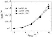
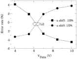
图3A示出数据写入期间的扫描信号的脉宽为第一持续期间时,数据信号的电压值与流经发光二极管的电流值之间的曲线图,图3B示出图3A中的扫描信号的脉宽漂移+10%与-10%与标准脉宽分别进行比较时,数据信号的电压值与误差率的曲线图。Fig. 3A shows the graph between the voltage value of the data signal and the current value flowing through the light-emitting diode when the pulse width of the scan signal during the data writing period is the first duration, and Fig. 3B shows the scan signal in Fig. 3A When the pulse width drift +10% and -10% are compared with the standard pulse width respectively, the curve graph of the voltage value and error rate of the data signal.
参照图3A和图3B,数据写入期间内的扫描信号GL脉宽w为0.4us。当该脉宽漂移+10%与-10%时,透过数据信号的电压值与流经发光二极管的电流值的曲线可知,在数据信号的电压值较低时,正漂移或负漂移10%与未出现漂移时的曲线拟合度较高。随着数据信号的电压值增加,正漂移或负漂移10%与未出现漂移时的曲线差距较大。此外,透过图3B也可知晓,椭圆框L1为正漂移10%与负漂移10%的交叉位置亦出现在数据信号的电压值较低的区间范围。较佳地,数据信号在该电压值范围时,针对迁移率漂移的补偿误差在3%以内。Referring to FIG. 3A and FIG. 3B , the pulse width w of the scan signal GL during the data writing period is 0.4 us. When the pulse width drifts +10% and -10%, through the curve of the voltage value of the data signal and the current value flowing through the LED, it can be seen that when the voltage value of the data signal is low, the positive drift or negative drift is 10%. The curve fitting degree is high when there is no drift. As the voltage value of the data signal increases, there is a large gap between the curves with positive or negative drift of 10% and no drift. In addition, it can also be known from FIG. 3B that the intersection position of the oval frame L1 with a positive drift of 10% and a negative drift of 10% also appears in the range of the lower voltage value of the data signal. Preferably, when the data signal is in the voltage value range, the compensation error for the mobility drift is within 3%.
图4A示出数据写入期间的扫描信号的脉宽为第二持续期间时,数据信号的电压值与流经发光二极管的电流值之间的曲线图,图4B示出图4A中的扫描信号的脉宽漂移+10%与-10%与标准脉宽分别进行比较时,数据信号的电压值与误差率的曲线图。Figure 4A shows the graph between the voltage value of the data signal and the current value flowing through the light-emitting diode when the pulse width of the scan signal during the data writing period is the second duration, and Figure 4B shows the scan signal in Figure 4A When the pulse width drift +10% and -10% are compared with the standard pulse width respectively, the curve graph of the voltage value and error rate of the data signal.
类似于图3A和图3B,在图4A和图4B中,数据写入期间内的扫描信号GL脉宽w为0.6us。透过图4B可知,椭圆框L2为正漂移10%与负漂移10%的交叉位置出现在数据信号的电压值较低的区间范围,但该电压区间范围大于图3B中的电压区间范围。也就是说,在该电压区间范围内,数据写入期间内的扫描信号GL脉宽w为0.6us较0.4us能够更好地补偿或消除薄膜晶体管的迁移率变异。同样,数据信号在该电压值范围时,针对迁移率漂移的补偿误差也在3%以内。Similar to FIG. 3A and FIG. 3B , in FIG. 4A and FIG. 4B , the pulse width w of the scanning signal GL during the data writing period is 0.6 us. It can be seen from FIG. 4B that the cross position of the elliptical frame L2 with a positive drift of 10% and a negative drift of 10% appears in the lower voltage range of the data signal, but the voltage range is larger than the voltage range in FIG. 3B . That is to say, within the range of the voltage range, the scan signal GL pulse width w of 0.6 us in the data writing period can better compensate or eliminate the mobility variation of the thin film transistor than 0.4 us. Similarly, when the data signal is in the voltage range, the compensation error for the mobility drift is also within 3%.
图5A示出数据写入期间的扫描信号的脉宽为第三持续期间时,数据信号的电压值与流经发光二极管的电流值之间的曲线图,图5B示出图5A中的扫描信号的脉宽漂移+10%与-10%与标准脉宽分别进行比较时,数据信号的电压值与误差率的曲线图。Figure 5A shows the graph between the voltage value of the data signal and the current value flowing through the light-emitting diode when the pulse width of the scan signal during the data writing period is the third duration, and Figure 5B shows the scan signal in Figure 5A When the pulse width drift +10% and -10% are compared with the standard pulse width respectively, the curve graph of the voltage value and error rate of the data signal.
类似于图3A和图3B,在图5A和图5B中,数据写入期间内的扫描信号GL脉宽w为0.8us。透过图5B可知,椭圆框L3为正漂移10%与负漂移10%的交叉位置出现在数据信号的电压值较高的区间范围,并且该电压区间范围大于图3B和图4B的电压区间范围。也就是说,在该电压区间范围内,数据写入期间内的扫描信号GL脉宽w为0.8us较0.6us及4us能够更好地补偿或消除薄膜晶体管的迁移率变异。此外,在图5B中,透过数据信号的电压值与流经发光二极管的电流值的曲线可知,在数据信号的电压值较低时,正漂移或负漂移10%与未出现漂移时的曲线相差甚大。Similar to FIG. 3A and FIG. 3B , in FIG. 5A and FIG. 5B , the pulse width w of the scanning signal GL during the data writing period is 0.8 us. It can be seen from Fig. 5B that the intersection position of the elliptical frame L3 with a positive drift of 10% and a negative drift of 10% appears in the range of the higher voltage value of the data signal, and the range of the voltage range is larger than the range of the voltage range in Fig. 3B and Fig. 4B . That is to say, within the range of the voltage range, the scanning signal GL pulse width w of 0.8 us in the data writing period can better compensate or eliminate the mobility variation of the thin film transistor than 0.6 us and 4 us. In addition, in FIG. 5B , through the curves of the voltage value of the data signal and the current value flowing through the light-emitting diode, it can be seen that when the voltage value of the data signal is low, the curves when there is a positive or negative drift of 10% and no drift Very different.
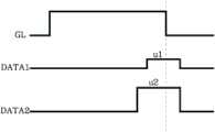
图6示出数据信号的不同电压值与流经发光二极管的电流值之间的非连续曲线的示意图。图7示出扫描信号相同条件下,薄膜晶体管的迁移率补偿时间与数据信号相关的示意图。FIG. 6 shows a schematic diagram of discontinuous curves between different voltage values of the data signal and current values flowing through the LED. FIG. 7 shows a schematic diagram of the correlation between the mobility compensation time of the thin film transistor and the data signal under the same condition of the scanning signal.
如图6所示,数据信号的电压值大小(VData)与流经发光二极管的电流值(IOLED)的关系曲线包括多条非连续的曲线段。与此同时,对于相邻两个曲线段的电流重叠部分,以查找表(Look-up Table)方式,灰阶电压写至a值后直接跳转至b值,在a值与b值之间的范围并不执行任何操作。此外,在图7中,根据扫描信号GL的下降沿,不同数据信号DATA1和DATA2所对应的迁移率消除时间u1和u2亦不相同。也就是说,在扫描信号GL的脉冲宽度一定的条件下,迁移率消除时间仅仅只与数据信号相关。As shown in FIG. 6 , the relationship curve between the voltage value (VData ) of the data signal and the current value (IOLED ) flowing through the light emitting diode includes a plurality of discontinuous curve segments. At the same time, for the current overlapping part of two adjacent curve segments, in the way of look-up table (Look-up Table), after the gray-scale voltage is written to the value a, it directly jumps to the value b, and between the value a and the value b The range does nothing. In addition, in FIG. 7 , according to the falling edge of the scanning signal GL, the mobility canceling times u1 and u2 corresponding to different data signals DATA1 and DATA2 are also different. That is to say, under the condition that the pulse width of the scanning signal GL is constant, the mobility cancellation time is only related to the data signal.
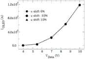
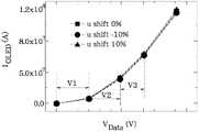
图8示出采用本发明的像素补偿电路在所有灰阶范围内对薄膜晶体管的迁移率进行补偿时,数据信号的电压值与流经发光二极管的电流值之间的曲线示意图。图9示出图8中的扫描信号的脉宽漂移+10%与-10%与标准脉宽分别进行比较时,数据信号的电压值与误差率的曲线图。FIG. 8 shows a schematic diagram of the curve between the voltage value of the data signal and the current value flowing through the light emitting diode when the pixel compensation circuit of the present invention is used to compensate the mobility of the thin film transistor in all gray scale ranges. FIG. 9 shows a graph of the voltage value and error rate of the data signal when the pulse width drift +10% and −10% of the scanning signal in FIG. 8 are compared with the standard pulse width respectively.
参照图8和图9,当数据信号的电压值介于4V~5.5V(电压区间V1)时,扫描信号的脉冲宽度为0.4us。数据信号的电压值介于5.55V~7V(电压区间V2)时,扫描信号的脉冲宽度为0.6us。数据信号的电压值介于7.4V~10V(电压区间V3)时,扫描信号的脉冲宽度为0.8us。从图9也可进一步看出,采用本发明的像素补偿电路,透过不同数据信号的电压值与扫描信号的不同脉冲宽度之间的匹配关系,可在所有灰阶范围内都改善薄膜晶体管的迁移率变异,消除面板不均匀现象。并且,数据信号在所有灰阶电压范围内,针对迁移率漂移的补偿误差均控制在3%以内。Referring to FIG. 8 and FIG. 9 , when the voltage value of the data signal is between 4V-5.5V (voltage range V1 ), the pulse width of the scan signal is 0.4us. When the voltage value of the data signal is between 5.55V-7V (voltage range V2), the pulse width of the scanning signal is 0.6us. When the voltage value of the data signal is between 7.4V-10V (voltage interval V3), the pulse width of the scan signal is 0.8us. It can be further seen from FIG. 9 that, by using the pixel compensation circuit of the present invention, through the matching relationship between the voltage values of different data signals and the different pulse widths of scanning signals, the performance of thin film transistors can be improved in all gray scale ranges. Mobility variation to eliminate panel inhomogeneity. Moreover, the compensation error for the mobility drift of the data signal is controlled within 3% in all gray scale voltage ranges.
采用本发明的像素补偿电路,第一晶体管的控制端用以接收一扫描信号且第一端用以接收一数据信号,第二晶体管的控制端电性耦接第一晶体管的第二端,第二晶体管的第二端用以接收一控制信号,发光二极管的阳极电性连接至第二晶体管的第一端且阴极电性连接至一接地电压。在数据写入期间,扫描信号的脉冲宽度根据数据信号的大小进行调节,从而补偿薄膜晶体管的迁移率。相比于现有技术,本发明像素补偿电路的扫描信号在数据写入期间可根据数据信号的大小进行调节,不同数据信号的电压值对应于不同的扫描信号的脉冲宽度,因此能够在所有灰阶范围内都改善薄膜晶体管的迁移率变异,消除面板不均匀现象,提升面板的图像显示品质。Using the pixel compensation circuit of the present invention, the control end of the first transistor is used to receive a scan signal and the first end is used to receive a data signal, the control end of the second transistor is electrically coupled to the second end of the first transistor, and the second transistor is electrically coupled to the second end of the first transistor. The second end of the two transistors is used to receive a control signal, the anode of the LED is electrically connected to the first end of the second transistor and the cathode is electrically connected to a ground voltage. During data writing, the pulse width of the scan signal is adjusted according to the magnitude of the data signal, thereby compensating the mobility of the thin film transistor. Compared with the prior art, the scanning signal of the pixel compensation circuit of the present invention can be adjusted according to the size of the data signal during data writing, and the voltage values of different data signals correspond to the pulse widths of different scanning signals, so it can be used in all gray The mobility variation of the thin film transistor is improved within the order range, the unevenness of the panel is eliminated, and the image display quality of the panel is improved.
上文中,参照附图描述了本发明的具体实施方式。但是,本领域中的普通技术人员能够理解,在不偏离本发明的精神和范围的情况下,还可以对本发明的具体实施方式作各种变更和替换。这些变更和替换都落在本发明权利要求书所限定的范围内。Hereinbefore, specific embodiments of the present invention have been described with reference to the accompanying drawings. However, those skilled in the art can understand that without departing from the spirit and scope of the present invention, various changes and substitutions can be made to the specific embodiments of the present invention. These changes and substitutions all fall within the scope defined by the claims of the present invention.
Claims (9)
Priority Applications (1)
| Application Number | Priority Date | Filing Date | Title |
|---|---|---|---|
| CN201410032056.5ACN103730091A (en) | 2014-01-23 | 2014-01-23 | Pixel compensation circuit |
Applications Claiming Priority (1)
| Application Number | Priority Date | Filing Date | Title |
|---|---|---|---|
| CN201410032056.5ACN103730091A (en) | 2014-01-23 | 2014-01-23 | Pixel compensation circuit |
Publications (1)
| Publication Number | Publication Date |
|---|---|
| CN103730091Atrue CN103730091A (en) | 2014-04-16 |
Family
ID=50454141
Family Applications (1)
| Application Number | Title | Priority Date | Filing Date |
|---|---|---|---|
| CN201410032056.5APendingCN103730091A (en) | 2014-01-23 | 2014-01-23 | Pixel compensation circuit |
Country Status (1)
| Country | Link |
|---|---|
| CN (1) | CN103730091A (en) |
Cited By (6)
| Publication number | Priority date | Publication date | Assignee | Title |
|---|---|---|---|---|
| CN104537985A (en)* | 2015-01-19 | 2015-04-22 | 深圳市华星光电技术有限公司 | Organic illuminating display panel and drop compensation method thereof |
| CN108615505A (en)* | 2018-05-14 | 2018-10-02 | 京东方科技集团股份有限公司 | The parameter method for detecting and device of driving transistor, compensation method |
| CN109935213A (en)* | 2017-12-15 | 2019-06-25 | 京东方科技集团股份有限公司 | Brightness adjustment method of display panel, display panel and driving method thereof |
| CN112289255A (en)* | 2019-12-24 | 2021-01-29 | 友达光电股份有限公司 | Display panel and pixel circuit thereof |
| CN114677981A (en)* | 2022-03-28 | 2022-06-28 | Tcl华星光电技术有限公司 | Charging compensation method and charging compensation device |
| CN115424574A (en)* | 2022-05-18 | 2022-12-02 | 友达光电股份有限公司 | Pixel circuit |
- 2014
- 2014-01-23CNCN201410032056.5Apatent/CN103730091A/enactivePending
Cited By (8)
| Publication number | Priority date | Publication date | Assignee | Title |
|---|---|---|---|---|
| CN104537985A (en)* | 2015-01-19 | 2015-04-22 | 深圳市华星光电技术有限公司 | Organic illuminating display panel and drop compensation method thereof |
| CN104537985B (en)* | 2015-01-19 | 2017-06-30 | 深圳市华星光电技术有限公司 | A kind of organic electroluminescence display panel and its voltage-drop compensation method |
| CN109935213A (en)* | 2017-12-15 | 2019-06-25 | 京东方科技集团股份有限公司 | Brightness adjustment method of display panel, display panel and driving method thereof |
| CN108615505A (en)* | 2018-05-14 | 2018-10-02 | 京东方科技集团股份有限公司 | The parameter method for detecting and device of driving transistor, compensation method |
| CN112289255A (en)* | 2019-12-24 | 2021-01-29 | 友达光电股份有限公司 | Display panel and pixel circuit thereof |
| CN112289255B (en)* | 2019-12-24 | 2022-11-22 | 友达光电股份有限公司 | Display panel and its pixel circuit |
| CN114677981A (en)* | 2022-03-28 | 2022-06-28 | Tcl华星光电技术有限公司 | Charging compensation method and charging compensation device |
| CN115424574A (en)* | 2022-05-18 | 2022-12-02 | 友达光电股份有限公司 | Pixel circuit |
Similar Documents
| Publication | Publication Date | Title |
|---|---|---|
| CN103165080B (en) | Pixel circuit and driving method and display device thereof | |
| CN104050923B (en) | Pixel circuit and display device using the same | |
| KR101411619B1 (en) | Pixel circuit and method for driving thereof, and organic light emitting display device using the same | |
| TWI533278B (en) | Pixel structure and driving method thereof | |
| US9634070B2 (en) | Organic light emitting display device | |
| CN204680360U (en) | A kind of image element circuit and display device | |
| KR101352119B1 (en) | Organic light emitting diode display | |
| US20160078816A1 (en) | Compensation of threshold voltage in driving transistor of organic light emitting diode display device | |
| US9842538B2 (en) | Organic light emitting display device and method for driving the same | |
| US9299756B2 (en) | Organic light emitting display device | |
| CN103730091A (en) | Pixel compensation circuit | |
| CN102982766A (en) | A pixel compensation circuit | |
| TWI594221B (en) | Pixel structure and driving method thereof | |
| CN103035202A (en) | Pixel compensation circuit | |
| CN104637446B (en) | Image element circuit and its driving method and a kind of display device | |
| CN104680977A (en) | A Pixel Compensation Circuit for High Resolution AMOLED | |
| CN103956142B (en) | Panel drive circuit and panel driving method | |
| CN103229227B (en) | Driving method of display device | |
| CN104318899B (en) | Pixel unit driving circuit and method, pixel unit and display device | |
| WO2016150079A1 (en) | Oled display device and method for correcting residual image of oled display device | |
| CN104021763A (en) | Pixel circuit, display device and drive method of pixel circuit | |
| CN104282268A (en) | Pixel Compensation Circuit for Active Matrix Organic Light Emitting Diode Display | |
| CN102867479B (en) | Compensation circuit for maintaining luminous brightness of diode | |
| KR20210086331A (en) | Electroluminescent display apparatus | |
| CN104464624A (en) | Pixel compensation circuit of active matrix organic light emitting diode display |
Legal Events
| Date | Code | Title | Description |
|---|---|---|---|
| C06 | Publication | ||
| PB01 | Publication | ||
| WD01 | Invention patent application deemed withdrawn after publication | ||
| WD01 | Invention patent application deemed withdrawn after publication | Application publication date:20140416 |