CN103715268A - Oxide thin-film transistor and display device - Google Patents
Oxide thin-film transistor and display deviceDownload PDFInfo
- Publication number
- CN103715268A CN103715268ACN201310750079.5ACN201310750079ACN103715268ACN 103715268 ACN103715268 ACN 103715268ACN 201310750079 ACN201310750079 ACN 201310750079ACN 103715268 ACN103715268 ACN 103715268A
- Authority
- CN
- China
- Prior art keywords
- oxide
- layer
- active layer
- film transistor
- etch stop
- Prior art date
- Legal status (The legal status is an assumption and is not a legal conclusion. Google has not performed a legal analysis and makes no representation as to the accuracy of the status listed.)
- Granted
Links
Images


Classifications
- H—ELECTRICITY
- H10—SEMICONDUCTOR DEVICES; ELECTRIC SOLID-STATE DEVICES NOT OTHERWISE PROVIDED FOR
- H10D—INORGANIC ELECTRIC SEMICONDUCTOR DEVICES
- H10D30/00—Field-effect transistors [FET]
- H10D30/60—Insulated-gate field-effect transistors [IGFET]
- H10D30/67—Thin-film transistors [TFT]
- H10D30/674—Thin-film transistors [TFT] characterised by the active materials
- H10D30/6755—Oxide semiconductors, e.g. zinc oxide, copper aluminium oxide or cadmium stannate
- H—ELECTRICITY
- H10—SEMICONDUCTOR DEVICES; ELECTRIC SOLID-STATE DEVICES NOT OTHERWISE PROVIDED FOR
- H10D—INORGANIC ELECTRIC SEMICONDUCTOR DEVICES
- H10D30/00—Field-effect transistors [FET]
- H10D30/60—Insulated-gate field-effect transistors [IGFET]
- H10D30/67—Thin-film transistors [TFT]
- H10D30/6704—Thin-film transistors [TFT] having supplementary regions or layers in the thin films or in the insulated bulk substrates for controlling properties of the device
- H10D30/6713—Thin-film transistors [TFT] having supplementary regions or layers in the thin films or in the insulated bulk substrates for controlling properties of the device characterised by the properties of the source or drain regions, e.g. compositions or sectional shapes
- H—ELECTRICITY
- H10—SEMICONDUCTOR DEVICES; ELECTRIC SOLID-STATE DEVICES NOT OTHERWISE PROVIDED FOR
- H10D—INORGANIC ELECTRIC SEMICONDUCTOR DEVICES
- H10D86/00—Integrated devices formed in or on insulating or conducting substrates, e.g. formed in silicon-on-insulator [SOI] substrates or on stainless steel or glass substrates
- H10D86/40—Integrated devices formed in or on insulating or conducting substrates, e.g. formed in silicon-on-insulator [SOI] substrates or on stainless steel or glass substrates characterised by multiple TFTs
- H10D86/60—Integrated devices formed in or on insulating or conducting substrates, e.g. formed in silicon-on-insulator [SOI] substrates or on stainless steel or glass substrates characterised by multiple TFTs wherein the TFTs are in active matrices
Landscapes
- Thin Film Transistor (AREA)
Abstract
Translated fromChinese
Description
Translated fromChinese技术领域technical field
本发明涉及半导体技术领域,具体涉及一种氧化物薄膜晶体管及显示装置。The invention relates to the technical field of semiconductors, in particular to an oxide thin film transistor and a display device.
背景技术Background technique
氧化物薄膜晶体管(Oxide TFT)由于其较高的迁移率,被广泛应用于大尺寸、高PPI(Pixels per inch,每英寸像素数)的LCD(液晶显示器)及OLED(Organic Light Emitting Diode,有机发光二极管)产品中。Oxide thin film transistor (Oxide TFT) is widely used in large-size, high PPI (Pixels per inch, pixels per inch) LCD (liquid crystal display) and OLED (Organic Light Emitting Diode, organic light-emitting diode) products.
目前的氧化物薄膜晶体管的结构如图1所示,在薄膜晶体管基板11上形成栅极12,在栅极12上形成栅极绝缘层13,在栅极绝缘层13上形成氧化物有源层14,在氧化物有源层14上形成蚀刻阻挡层15,蚀刻阻挡层15上形成有开口,源/漏电极16通过该开口直接与氧化物有源层14接触。其中,氧化物有源层14通常由IGZO(Indium Gallium Zinc oxide,铟镓锌氧化物)构成,栅极绝缘层13和蚀刻阻挡层15通常由氧化硅构成。The structure of the current oxide thin film transistor is shown in FIG. 1. A
由于源/漏电极直接与氧化物有源层接触,接触电阻较大,使得接触特性较差,导致薄膜晶体管的开态电流(Ion)较小;同时直接接触还使得氧化物有源层界面缺陷较高,导致薄膜晶体管的关态电流(Ioff)较大,从而使得薄膜晶体管的Ion/Ioff较小,严重影响了薄膜晶体管的性能,进而影响显示装置的性能。Since the source/drain electrodes are directly in contact with the oxide active layer, the contact resistance is large, which makes the contact characteristics poor, resulting in a small on-state current (Ion ) of the thin film transistor; at the same time, the direct contact also makes the oxide active layer interface Higher defects lead to a larger off-state current (Ioff ) of the thin film transistor, thereby making the Ion /Ioff of the thin film transistor smaller, seriously affecting the performance of the thin film transistor, and further affecting the performance of the display device.
发明内容Contents of the invention
本发明所要解决的技术问题是提高薄膜晶体管的开态电流与关态电流之比。The technical problem to be solved by the invention is to increase the ratio of the on-state current to the off-state current of the thin film transistor.
为此目的,根据本发明的第一方面,提出了一种氧化物薄膜晶体管,包括:基板;栅极,形成在所述基板上;栅极绝缘层,形成在所述栅极上;氧化物有源层,形成在所述栅极绝缘层上;蚀刻阻挡层,形成在所述氧化物有源层上,且所述蚀刻阻挡层上具有开口;源/漏电极,形成在所述蚀刻阻挡层上,所述源/漏电极通过接触层、并经由所述蚀刻阻挡层上的所述开口与所述氧化物有源层电连接;其中,所述接触层由与所述氧化物有源层相同成分的氧化物材料制成,所述接触层与所述氧化物有源层的氧化物材料的含氧量不同,所述接触层表现为导体特性,所述氧化物有源层表现为半导体特性。For this purpose, according to the first aspect of the present invention, an oxide thin film transistor is proposed, comprising: a substrate; a gate formed on the substrate; a gate insulating layer formed on the gate; an oxide an active layer formed on the gate insulating layer; an etch stop layer formed on the oxide active layer with openings; a source/drain electrode formed on the etch stop layer, the source/drain electrode is electrically connected to the oxide active layer through the contact layer and through the opening on the etch barrier layer; wherein, the contact layer is connected to the oxide active layer. The contact layer and the oxide material of the oxide active layer are made of oxide materials with the same composition, the oxygen content of the oxide material of the contact layer is different from that of the oxide active layer, the contact layer exhibits conductor characteristics, and the oxide active layer exhibits Semiconductor properties.
优选地,所述栅极绝缘层和/或所述蚀刻阻挡层由所述相同成分的氧化物材料制成,所述栅极绝缘层和/或所述蚀刻阻挡层的氧化物材料与所述氧化物有源层的氧化物材料的含氧量不同,所述栅极绝缘层和/或所述蚀刻阻挡层表现为绝缘介质特性。Preferably, the gate insulating layer and/or the etch stop layer are made of oxide materials of the same composition, and the oxide material of the gate insulating layer and/or the etch stop layer is the same as the oxide material of the etch stop layer. Oxygen content of the oxide material of the oxide active layer is different, and the gate insulating layer and/or the etching stopper layer exhibit insulating dielectric properties.
优选地,所述栅极绝缘层与所述氧化物有源层之间和/或所述蚀刻阻挡层与所述氧化物有源层之间还包括由所述相同成分的氧化物材料制成的过渡层,所述过渡层的氧化物材料与所述氧化物有源层的氧化物材料的含氧量不同,所述过渡层表现为绝缘介质特性。Preferably, between the gate insulating layer and the oxide active layer and/or between the etching stopper layer and the oxide active layer, there is an oxide material made of the same composition. The transition layer, the oxide material of the transition layer is different from the oxygen content of the oxide material of the oxide active layer, and the transition layer exhibits insulating dielectric properties.
优选地,所述相同成分的氧化物材料为IGZO。Preferably, the oxide material of the same composition is IGZO.
根据本发明的第二方面,提出了一种氧化物薄膜晶体管,包括:基板;栅极,形成在所述基板上;栅极绝缘层,形成在所述栅极上;氧化物有源层,形成在所述栅极绝缘层上;蚀刻阻挡层,形成在所述氧化物有源层上,且所述蚀刻阻挡层上具有开口;源/漏电极,形成在所述蚀刻阻挡层上,所述源/漏电极经由所述蚀刻阻挡层上的所述开口与所述氧化物有源层电连接;其中,所述栅极绝缘层和/或所述蚀刻阻挡层由与所述氧化物有源层相同成分的氧化物材料制成,所述栅极绝缘层和/或所述蚀刻阻挡层的氧化物材料的含氧量与所述氧化物有源层的氧化物材料的含氧量不同,所述氧化物有源层表现为半导体特性,所述栅极绝缘层和/或所述蚀刻阻挡层表现为绝缘介质特性。According to the second aspect of the present invention, an oxide thin film transistor is proposed, comprising: a substrate; a gate formed on the substrate; a gate insulating layer formed on the gate; an oxide active layer, formed on the gate insulating layer; an etching barrier layer formed on the oxide active layer, and has an opening on the etching barrier layer; a source/drain electrode is formed on the etching barrier layer, the The source/drain electrode is electrically connected to the oxide active layer via the opening on the etching barrier layer; wherein, the gate insulating layer and/or the etching barrier layer are The source layer is made of an oxide material with the same composition, and the oxygen content of the oxide material of the gate insulating layer and/or the etching stopper layer is different from the oxygen content of the oxide material of the oxide active layer. , the oxide active layer exhibits semiconductor properties, and the gate insulating layer and/or the etch stop layer exhibits insulating dielectric properties.
优选地,所述源/漏电极与所述氧化物有源层之间还包括接触层,所述源/漏电极通过所述接触层与所述氧化物有源层电连接,所述接触层由与所述氧化物有源层相同成分的氧化物材料制成,所述接触层与所述氧化物有源层、所述栅极绝缘层、所述蚀刻阻挡层的氧化物材料的含氧量不同,所述接触层表现为导体特性。Preferably, a contact layer is further included between the source/drain electrode and the oxide active layer, the source/drain electrode is electrically connected to the oxide active layer through the contact layer, and the contact layer Made of an oxide material with the same composition as the oxide active layer, the oxygen-containing oxide material of the contact layer and the oxide active layer, the gate insulating layer, and the etch stop layer With different quantities, the contact layer behaves as a conductor.
优选地,所述相同成分的氧化物材料为IGZO。Preferably, the oxide material of the same composition is IGZO.
根据本发明的第三方面,提出了一种氧化物薄膜晶体管,包括:基板;栅极,形成在所述基板上;栅极绝缘层,形成在所述栅极上;氧化物有源层,形成在所述栅极绝缘层上;蚀刻阻挡层,形成在所述氧化物有源层上,且所述蚀刻阻挡层上具有开口;源/漏电极,形成在所述蚀刻阻挡层上,所述源/漏电极经由所述蚀刻阻挡层上的所述开口与所述氧化物有源层电连接;其中,所述栅极绝缘层与所述氧化物有源层之间和/或所述蚀刻阻挡层与所述氧化物有源层之间还包括由与所述氧化物有源层相同成分的氧化物材料制成的过渡层,所述过渡层的氧化物材料与所述氧化物有源层的氧化物材料的含氧量不同,所述氧化物有源层表现为半导体特性,所述过渡层表现为绝缘介质特性。According to a third aspect of the present invention, an oxide thin film transistor is proposed, comprising: a substrate; a gate formed on the substrate; a gate insulating layer formed on the gate; an oxide active layer, formed on the gate insulating layer; an etching barrier layer formed on the oxide active layer, and has an opening on the etching barrier layer; a source/drain electrode is formed on the etching barrier layer, the The source/drain electrode is electrically connected to the oxide active layer through the opening on the etching barrier layer; wherein, between the gate insulating layer and the oxide active layer and/or the A transition layer made of an oxide material having the same composition as that of the oxide active layer is also included between the etch barrier layer and the oxide active layer, and the oxide material of the transition layer is related to the oxide Oxygen content of the oxide material of the source layer is different, the oxide active layer exhibits semiconductor properties, and the transition layer exhibits insulating dielectric properties.
优选地,所述源/漏电极与所述氧化物有源层之间还包括接触层,所述源/漏电极通过所述接触层与所述氧化物有源层电连接,所述接触层由与所述氧化物有源层相同成分的氧化物材料制成,所述接触层与所述氧化物有源层、所述过渡层的氧化物材料的含氧量不同,所述接触层表现为导体特性。Preferably, a contact layer is further included between the source/drain electrode and the oxide active layer, the source/drain electrode is electrically connected to the oxide active layer through the contact layer, and the contact layer Made of an oxide material with the same composition as the oxide active layer, the contact layer has a different oxygen content from the oxide material of the oxide active layer and the transition layer, and the contact layer exhibits is the conductor characteristic.
优选地,所述相同成分的氧化物材料为IGZO。Preferably, the oxide material of the same composition is IGZO.
根据本发明的第四方面,提出了一种显示装置,包括上述的氧化物薄膜晶体管。According to a fourth aspect of the present invention, a display device is provided, including the above-mentioned oxide thin film transistor.
通过采用本发明所公开的氧化物薄膜晶体管,改善了电极接触特性和有源层的界面的匹配性,提升了氧化物薄膜晶体管的开态电流与关态电流之比,因此显著提高了包括该氧化物薄膜晶体管的显示装置的显示效果。By adopting the oxide thin film transistor disclosed in the present invention, the matching of the electrode contact characteristics and the interface of the active layer is improved, and the ratio of the on-state current to the off-state current of the oxide thin film transistor is improved, thereby significantly improving the The display effect of the display device of the oxide thin film transistor.
附图说明Description of drawings
通过参考附图会更加清楚的理解本发明的特征和优点,附图是示意性的而不应理解为对本发明进行任何限制,在附图中:The features and advantages of the present invention will be more clearly understood by referring to the accompanying drawings, which are schematic and should not be construed as limiting the invention in any way. In the accompanying drawings:
图1示出了目前的氧化物薄膜晶体管的示意图;FIG. 1 shows a schematic diagram of a current oxide thin film transistor;
图2示出了根据本发明第一实施例的氧化物薄膜晶体管的示意图;FIG. 2 shows a schematic diagram of an oxide thin film transistor according to a first embodiment of the present invention;
图3示出了根据本发明第二实施例的氧化物薄膜晶体管的示意图;FIG. 3 shows a schematic diagram of an oxide thin film transistor according to a second embodiment of the present invention;
图4示出了根据本发明第三实施例的氧化物薄膜晶体管的示意图。FIG. 4 shows a schematic diagram of an oxide thin film transistor according to a third embodiment of the present invention.
具体实施方式Detailed ways
下面将结合附图对本发明的实施例进行详细描述。Embodiments of the present invention will be described in detail below with reference to the accompanying drawings.
图2示出了根据本发明第一实施例的氧化物薄膜晶体管的示意图,如图2所示,类似于现有的氧化物薄膜晶体管,栅极22形成在薄膜晶体管基板21上,栅极绝缘层23形成在栅极22上,氧化物有源层24形成在栅极绝缘层23上,蚀刻阻挡层25形成在氧化物有源层24上,通过光刻和刻蚀工艺,在蚀刻阻挡层25上形成开口。在这里,氧化物有源层24优选由IGZO构成。然后在蚀刻阻挡层25上形成IGZO接触层27和源/漏极金属层26,并通过光刻和刻蚀工艺形成薄膜晶体管的源极和漏极电极。FIG. 2 shows a schematic diagram of an oxide thin film transistor according to a first embodiment of the present invention. As shown in FIG. 2, similar to an existing oxide thin film transistor, a gate 22 is formed on a thin film transistor substrate 21, and the gate is insulated. The layer 23 is formed on the gate 22, the oxide active layer 24 is formed on the gate insulating layer 23, the etch barrier layer 25 is formed on the oxide active layer 24, and through the photolithography and etching process, the etch barrier layer Opening is formed on 25. Here, the oxide active layer 24 is preferably composed of IGZO. Then an IGZO contact layer 27 and a source/drain metal layer 26 are formed on the etch barrier layer 25, and source and drain electrodes of the thin film transistor are formed by photolithography and etching processes.
对于IGZO材料而言,可以通过调整IGZO成膜过程中氧气(O2)的流量来实现IGZO绝缘介质、半导体及导体特性的转变。具体而言,IGZO采用溅射方式进行成膜,在溅射过程中主要采用氧气和氩气,为了得到不同特性的IGZO膜,氧气在混合气体中的含量在0-60%之间进行调节。For IGZO materials, the transformation of IGZO insulating medium, semiconductor and conductor characteristics can be realized by adjusting the flow rate of oxygen (O2 ) during IGZO film formation. Specifically, IGZO is formed by sputtering. Oxygen and argon are mainly used in the sputtering process. In order to obtain IGZO films with different characteristics, the content of oxygen in the mixed gas is adjusted between 0-60%.
具体而言,在制备IGZO膜时,当混合气体中的含氧量小于10%时,制成的IGZO材料表现为绝缘介质特性;当混合气体中的含氧量在10-30%时,制成的IGZO材料表现为半导体特性;当混合气体中的含氧量在30%以上时,制成的IGZO材料表现为导体特性。Specifically, when preparing the IGZO film, when the oxygen content in the mixed gas is less than 10%, the IGZO material produced exhibits insulating dielectric properties; when the oxygen content in the mixed gas is 10-30%, the prepared IGZO material The formed IGZO material exhibits semiconducting properties; when the oxygen content in the mixed gas is above 30%, the prepared IGZO material exhibits conducting properties.
在本实施例中,IGZO有源层24表现为半导体特性,IGZO接触层27表现为导体特性。由于源/漏电极26通过IGZO接触层27与IGZO有源层24接触,这类似于a-Si型薄膜晶体管器件中源/漏电极通过n+硅作为接触层而与有源层接触,由于IGZO接触层27与IGZO有源层24是相同成分的材料,仅含氧量不同,因此IGZO接触层27与IGZO有源层24之间表现出良好的接触特性,由此改善了薄膜晶体管的有源层与源/漏电极之间的接触特性,从而提升了薄膜晶体管的开态电流Ion。此外,由于IGZO接触层与IGZO有源层之间良好的接触特性,因此扩大了源/漏极金属层可采用的金属的范围,从而可以降低形成源/漏电极的工艺难度。In this embodiment, the IGZO active layer 24 exhibits semiconductor characteristics, and the IGZO contact layer 27 exhibits conductor characteristics. Because the source/drain electrode 26 is in contact with the IGZO active layer 24 through the IGZO contact layer 27, which is similar to that in the a-Si type thin film transistor device, the source/drain electrode is in contact with the active layer through n+ silicon as the contact layer, because the IGZO The contact layer 27 and the IGZO active layer 24 are materials of the same composition, and only the oxygen content is different, so good contact characteristics are shown between the IGZO contact layer 27 and the IGZO active layer 24, thereby improving the active properties of the thin film transistor. The contact characteristics between the layer and the source/drain electrodes, thereby improving the on-state current Ion of the thin film transistor. In addition, due to the good contact characteristics between the IGZO contact layer and the IGZO active layer, the range of metals that can be used for the source/drain metal layer is expanded, thereby reducing the process difficulty of forming the source/drain electrodes.
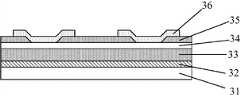
图3示出了根据本发明第二实施例的氧化物薄膜晶体管的示意图。如图3所示,在本实施例中,栅极绝缘层33和蚀刻阻挡层35由IGZO材料构成,通过控制形成栅极绝缘层33和蚀刻阻挡层35的IGZO材料中的含氧量使该IGZO材料表现出绝缘介质特性,由于IGZO栅极绝缘层33和IGZO蚀刻阻挡层35与IGZO有源层34是相同成分的材料,仅含氧量不同,因此提升了IGZO有源层34的界面的匹配性,从而减小了氧化物薄膜晶体管的关态电流Ioff。本领域技术人员应当理解,栅极绝缘层和蚀刻阻挡层之一采用绝缘的IGZO材料也是可行的,栅极绝缘层和蚀刻阻挡层的IGZO材料的含氧量可以相同也可以不同,只要表现为绝缘介质特性即可。FIG. 3 shows a schematic diagram of an oxide thin film transistor according to a second embodiment of the present invention. As shown in Figure 3, in this embodiment, the
图4示出了根据本发明第三实施例的氧化物薄膜晶体管的示意图。如图4所示,在栅极绝缘层43与IGZO有源层44之间以及IGZO有源层44与蚀刻阻挡层45之间还分别形成有IGZO绝缘层48和IGZO绝缘层49。基于相同的原理,提升了IGZO有源层44的界面的匹配性,从而减小了氧化物薄膜晶体管的关态电流Ioff。本领域技术人员应当理解,仅在栅极绝缘层43与氧化物有源层44之间或者仅在氧化物有源层44与蚀刻阻挡层45之间形成IGZO绝缘层也是可行的,IGZO绝缘层48和IGZO绝缘层49的含氧量可以相同也可以不同,只要表现为绝缘介质特性即可。FIG. 4 shows a schematic diagram of an oxide thin film transistor according to a third embodiment of the present invention. As shown in FIG. 4 , an
本领域技术人员还应当理解,上述实施例只是作为示例来说明本发明,并非对本发明进行任何限制。本领域技术人员可以对上述实施例的技术方案进行任意组合,从而提升薄膜晶体管的性能。Those skilled in the art should also understand that the above-mentioned embodiments are only used as examples to illustrate the present invention, and do not limit the present invention in any way. Those skilled in the art can make any combination of the technical solutions of the above embodiments, so as to improve the performance of the thin film transistor.
根据本发明实施例的氧化物薄膜晶体管可用于LCD或OLED显示装置中。由于根据本发明实施例的氧化物薄膜晶体管改善了电极接触特性和有源层的界面的匹配性,提升了氧化物薄膜晶体管的开态电流与关态电流之比,因此显著提高了显示装置的显示效果。The oxide thin film transistor according to the embodiments of the present invention can be used in LCD or OLED display devices. Since the oxide thin film transistor according to the embodiment of the present invention improves the matching of the electrode contact characteristics and the interface of the active layer, the ratio of the on-state current to the off-state current of the oxide thin film transistor is improved, thereby significantly improving the performance of the display device. display effect.
虽然结合附图描述了本发明的实施方式,但是本领域技术人员可以在不脱离本发明的精神和范围的情况下作出各种修改和变型,这样的修改和变型均落入由所附权利要求所限定的范围之内。Although the embodiments of the present invention have been described in conjunction with the accompanying drawings, those skilled in the art can make various modifications and variations without departing from the spirit and scope of the present invention. Such modifications and variations all fall into the scope of the appended claims. within the limited range.
Claims (11)
Priority Applications (1)
| Application Number | Priority Date | Filing Date | Title |
|---|---|---|---|
| CN201310750079.5ACN103715268B (en) | 2013-12-27 | 2013-12-27 | Oxide thin film transistor and display unit |
Applications Claiming Priority (1)
| Application Number | Priority Date | Filing Date | Title |
|---|---|---|---|
| CN201310750079.5ACN103715268B (en) | 2013-12-27 | 2013-12-27 | Oxide thin film transistor and display unit |
Publications (2)
| Publication Number | Publication Date |
|---|---|
| CN103715268Atrue CN103715268A (en) | 2014-04-09 |
| CN103715268B CN103715268B (en) | 2016-04-06 |
Family
ID=50408077
Family Applications (1)
| Application Number | Title | Priority Date | Filing Date |
|---|---|---|---|
| CN201310750079.5AActiveCN103715268B (en) | 2013-12-27 | 2013-12-27 | Oxide thin film transistor and display unit |
Country Status (1)
| Country | Link |
|---|---|
| CN (1) | CN103715268B (en) |
Cited By (4)
| Publication number | Priority date | Publication date | Assignee | Title |
|---|---|---|---|---|
| CN103985639A (en)* | 2014-04-28 | 2014-08-13 | 京东方科技集团股份有限公司 | Thin film transistor, manufacturing method thereof, display substrate and display device |
| CN104183605A (en)* | 2014-08-06 | 2014-12-03 | 京东方科技集团股份有限公司 | Display apparatus, and array substrate and manufacture method thereof |
| WO2020224011A1 (en)* | 2019-05-08 | 2020-11-12 | 深圳市华星光电半导体显示技术有限公司 | Oxide thin-film transistor device and manufacturing method therefor |
| CN115425070A (en)* | 2022-09-20 | 2022-12-02 | 昆山国显光电有限公司 | A kind of oxide thin film transistor, array substrate, display panel and electronic equipment |
Citations (6)
| Publication number | Priority date | Publication date | Assignee | Title |
|---|---|---|---|---|
| JP2010056540A (en)* | 2008-07-31 | 2010-03-11 | Semiconductor Energy Lab Co Ltd | Semiconductor device and manufacturing method thereof |
| US20100117073A1 (en)* | 2008-11-07 | 2010-05-13 | Shunpei Yamazaki | Semiconductor device and method for manufacturing the same |
| CN101872787A (en)* | 2010-05-19 | 2010-10-27 | 华南理工大学 | Metal oxide thin film transistor and preparation method thereof |
| CN102655165A (en)* | 2011-03-28 | 2012-09-05 | 京东方科技集团股份有限公司 | Amorphous-oxide thin-film transistor, manufacturing method thereof, and display panel |
| CN202443973U (en)* | 2012-02-28 | 2012-09-19 | 北京京东方光电科技有限公司 | Oxide semiconductor thin film transistor and display device |
| CN203631564U (en)* | 2013-12-27 | 2014-06-04 | 合肥京东方光电科技有限公司 | Oxide thin-film transistor and display device |
- 2013
- 2013-12-27CNCN201310750079.5Apatent/CN103715268B/enactiveActive
Patent Citations (6)
| Publication number | Priority date | Publication date | Assignee | Title |
|---|---|---|---|---|
| JP2010056540A (en)* | 2008-07-31 | 2010-03-11 | Semiconductor Energy Lab Co Ltd | Semiconductor device and manufacturing method thereof |
| US20100117073A1 (en)* | 2008-11-07 | 2010-05-13 | Shunpei Yamazaki | Semiconductor device and method for manufacturing the same |
| CN101872787A (en)* | 2010-05-19 | 2010-10-27 | 华南理工大学 | Metal oxide thin film transistor and preparation method thereof |
| CN102655165A (en)* | 2011-03-28 | 2012-09-05 | 京东方科技集团股份有限公司 | Amorphous-oxide thin-film transistor, manufacturing method thereof, and display panel |
| CN202443973U (en)* | 2012-02-28 | 2012-09-19 | 北京京东方光电科技有限公司 | Oxide semiconductor thin film transistor and display device |
| CN203631564U (en)* | 2013-12-27 | 2014-06-04 | 合肥京东方光电科技有限公司 | Oxide thin-film transistor and display device |
Cited By (5)
| Publication number | Priority date | Publication date | Assignee | Title |
|---|---|---|---|---|
| CN103985639A (en)* | 2014-04-28 | 2014-08-13 | 京东方科技集团股份有限公司 | Thin film transistor, manufacturing method thereof, display substrate and display device |
| CN103985639B (en)* | 2014-04-28 | 2015-06-03 | 京东方科技集团股份有限公司 | Thin film transistor, manufacturing method thereof, display substrate and display device |
| CN104183605A (en)* | 2014-08-06 | 2014-12-03 | 京东方科技集团股份有限公司 | Display apparatus, and array substrate and manufacture method thereof |
| WO2020224011A1 (en)* | 2019-05-08 | 2020-11-12 | 深圳市华星光电半导体显示技术有限公司 | Oxide thin-film transistor device and manufacturing method therefor |
| CN115425070A (en)* | 2022-09-20 | 2022-12-02 | 昆山国显光电有限公司 | A kind of oxide thin film transistor, array substrate, display panel and electronic equipment |
Also Published As
| Publication number | Publication date |
|---|---|
| CN103715268B (en) | 2016-04-06 |
Similar Documents
| Publication | Publication Date | Title |
|---|---|---|
| US10403757B2 (en) | Top-gate self-aligned metal oxide semiconductor TFT and method of making the same | |
| JP6134230B2 (en) | Thin film transistor and display device | |
| CN104620365B (en) | Thin film transistor and display device | |
| CN104022044B (en) | Oxide thin-film transistor and preparation method thereof, array substrate and display device | |
| CN104124277B (en) | A kind of thin film transistor (TFT) and preparation method thereof and array base palte | |
| CN106158978A (en) | Thin film transistor (TFT), array base palte and preparation method thereof | |
| CN106098560A (en) | The manufacture method of top gate type thin film transistor | |
| CN107516661B (en) | Display substrate, display device and manufacturing method of display substrate | |
| CN106971944A (en) | The preparation method and its structure of metal oxide thin-film transistor | |
| TWI640098B (en) | Semiconductor device and manufacturing method of semiconductor device | |
| CN103715268B (en) | Oxide thin film transistor and display unit | |
| CN104167447B (en) | A kind of thin film transistor (TFT) and preparation method thereof, display base plate and display device | |
| CN104167446B (en) | A kind of thin film transistor (TFT), array base palte and display device | |
| CN104143574A (en) | Active component | |
| CN104752517A (en) | Thin film transistor as well as preparation method and application of thin film transistor | |
| CN203631564U (en) | Oxide thin-film transistor and display device | |
| CN104157611B (en) | The manufacture method and its structure of oxide semiconductor TFT substrate | |
| WO2023123125A1 (en) | Array substrate, manufacturing method therefor, display panel and display apparatus | |
| CN104112671A (en) | Preparation method for zinc oxide thin-film transistor | |
| TW201340328A (en) | Thin film transistor | |
| CN104752515A (en) | Thin film transistor and manufacture method thereof |
Legal Events
| Date | Code | Title | Description |
|---|---|---|---|
| C06 | Publication | ||
| PB01 | Publication | ||
| C10 | Entry into substantive examination | ||
| SE01 | Entry into force of request for substantive examination | ||
| C14 | Grant of patent or utility model | ||
| GR01 | Patent grant |