CN103714856A - Memory system and read reclaim method thereof - Google Patents
Memory system and read reclaim method thereofDownload PDFInfo
- Publication number
- CN103714856A CN103714856ACN201310464864.4ACN201310464864ACN103714856ACN 103714856 ACN103714856 ACN 103714856ACN 201310464864 ACN201310464864 ACN 201310464864ACN 103714856 ACN103714856 ACN 103714856A
- Authority
- CN
- China
- Prior art keywords
- storage block
- storage
- data
- read
- block
- Prior art date
- Legal status (The legal status is an assumption and is not a legal conclusion. Google has not performed a legal analysis and makes no representation as to the accuracy of the status listed.)
- Granted
Links
Images


Classifications
- G—PHYSICS
- G11—INFORMATION STORAGE
- G11C—STATIC STORES
- G11C16/00—Erasable programmable read-only memories
- G11C16/02—Erasable programmable read-only memories electrically programmable
- G11C16/06—Auxiliary circuits, e.g. for writing into memory
- G—PHYSICS
- G06—COMPUTING OR CALCULATING; COUNTING
- G06F—ELECTRIC DIGITAL DATA PROCESSING
- G06F11/00—Error detection; Error correction; Monitoring
- G06F11/07—Responding to the occurrence of a fault, e.g. fault tolerance
- G06F11/08—Error detection or correction by redundancy in data representation, e.g. by using checking codes
- G06F11/10—Adding special bits or symbols to the coded information, e.g. parity check, casting out 9's or 11's
- G06F11/1008—Adding special bits or symbols to the coded information, e.g. parity check, casting out 9's or 11's in individual solid state devices
- G06F11/1068—Adding special bits or symbols to the coded information, e.g. parity check, casting out 9's or 11's in individual solid state devices in sector programmable memories, e.g. flash disk
- G—PHYSICS
- G06—COMPUTING OR CALCULATING; COUNTING
- G06F—ELECTRIC DIGITAL DATA PROCESSING
- G06F11/00—Error detection; Error correction; Monitoring
- G06F11/07—Responding to the occurrence of a fault, e.g. fault tolerance
- G06F11/08—Error detection or correction by redundancy in data representation, e.g. by using checking codes
- G06F11/10—Adding special bits or symbols to the coded information, e.g. parity check, casting out 9's or 11's
- G06F11/1008—Adding special bits or symbols to the coded information, e.g. parity check, casting out 9's or 11's in individual solid state devices
- G06F11/1072—Adding special bits or symbols to the coded information, e.g. parity check, casting out 9's or 11's in individual solid state devices in multilevel memories
- G—PHYSICS
- G06—COMPUTING OR CALCULATING; COUNTING
- G06F—ELECTRIC DIGITAL DATA PROCESSING
- G06F12/00—Accessing, addressing or allocating within memory systems or architectures
- G06F12/02—Addressing or allocation; Relocation
- G06F12/0223—User address space allocation, e.g. contiguous or non contiguous base addressing
- G06F12/023—Free address space management
- G06F12/0238—Memory management in non-volatile memory, e.g. resistive RAM or ferroelectric memory
- G06F12/0246—Memory management in non-volatile memory, e.g. resistive RAM or ferroelectric memory in block erasable memory, e.g. flash memory
- G—PHYSICS
- G06—COMPUTING OR CALCULATING; COUNTING
- G06F—ELECTRIC DIGITAL DATA PROCESSING
- G06F12/00—Accessing, addressing or allocating within memory systems or architectures
- G06F12/02—Addressing or allocation; Relocation
- G06F12/0223—User address space allocation, e.g. contiguous or non contiguous base addressing
- G06F12/023—Free address space management
- G06F12/0253—Garbage collection, i.e. reclamation of unreferenced memory
- G—PHYSICS
- G11—INFORMATION STORAGE
- G11C—STATIC STORES
- G11C11/00—Digital stores characterised by the use of particular electric or magnetic storage elements; Storage elements therefor
- G11C11/56—Digital stores characterised by the use of particular electric or magnetic storage elements; Storage elements therefor using storage elements with more than two stable states represented by steps, e.g. of voltage, current, phase, frequency
- G11C11/5621—Digital stores characterised by the use of particular electric or magnetic storage elements; Storage elements therefor using storage elements with more than two stable states represented by steps, e.g. of voltage, current, phase, frequency using charge storage in a floating gate
- G11C11/5628—Programming or writing circuits; Data input circuits
- G—PHYSICS
- G11—INFORMATION STORAGE
- G11C—STATIC STORES
- G11C11/00—Digital stores characterised by the use of particular electric or magnetic storage elements; Storage elements therefor
- G11C11/56—Digital stores characterised by the use of particular electric or magnetic storage elements; Storage elements therefor using storage elements with more than two stable states represented by steps, e.g. of voltage, current, phase, frequency
- G11C11/5621—Digital stores characterised by the use of particular electric or magnetic storage elements; Storage elements therefor using storage elements with more than two stable states represented by steps, e.g. of voltage, current, phase, frequency using charge storage in a floating gate
- G11C11/5642—Sensing or reading circuits; Data output circuits
- G—PHYSICS
- G11—INFORMATION STORAGE
- G11C—STATIC STORES
- G11C11/00—Digital stores characterised by the use of particular electric or magnetic storage elements; Storage elements therefor
- G11C11/56—Digital stores characterised by the use of particular electric or magnetic storage elements; Storage elements therefor using storage elements with more than two stable states represented by steps, e.g. of voltage, current, phase, frequency
- G11C11/5671—Digital stores characterised by the use of particular electric or magnetic storage elements; Storage elements therefor using storage elements with more than two stable states represented by steps, e.g. of voltage, current, phase, frequency using charge trapping in an insulator
- G—PHYSICS
- G11—INFORMATION STORAGE
- G11C—STATIC STORES
- G11C16/00—Erasable programmable read-only memories
- G11C16/02—Erasable programmable read-only memories electrically programmable
- G11C16/06—Auxiliary circuits, e.g. for writing into memory
- G11C16/10—Programming or data input circuits
- G—PHYSICS
- G11—INFORMATION STORAGE
- G11C—STATIC STORES
- G11C16/00—Erasable programmable read-only memories
- G11C16/02—Erasable programmable read-only memories electrically programmable
- G11C16/06—Auxiliary circuits, e.g. for writing into memory
- G11C16/26—Sensing or reading circuits; Data output circuits
- G—PHYSICS
- G11—INFORMATION STORAGE
- G11C—STATIC STORES
- G11C16/00—Erasable programmable read-only memories
- G11C16/02—Erasable programmable read-only memories electrically programmable
- G11C16/06—Auxiliary circuits, e.g. for writing into memory
- G11C16/34—Determination of programming status, e.g. threshold voltage, overprogramming or underprogramming, retention
- G—PHYSICS
- G11—INFORMATION STORAGE
- G11C—STATIC STORES
- G11C29/00—Checking stores for correct operation ; Subsequent repair; Testing stores during standby or offline operation
- G11C29/52—Protection of memory contents; Detection of errors in memory contents
Landscapes
- Engineering & Computer Science (AREA)
- Theoretical Computer Science (AREA)
- Physics & Mathematics (AREA)
- General Engineering & Computer Science (AREA)
- General Physics & Mathematics (AREA)
- Computer Hardware Design (AREA)
- Quality & Reliability (AREA)
- Read Only Memory (AREA)
- Memory System (AREA)
- Techniques For Improving Reliability Of Storages (AREA)
Abstract
Description
Translated fromChinese对相关申请的交叉引用Cross References to Related Applications
本申请要求于2012年10月5日在韩国知识产权局提交的韩国专利申请第10-2012-0110859号的优先权,其全部内容通过引用合并于此。This application claims priority from Korean Patent Application No. 10-2012-0110859 filed on Oct. 5, 2012 at the Korean Intellectual Property Office, the entire contents of which are hereby incorporated by reference.
技术领域technical field
这里描述的发明构思涉及半导体存储器件,更具体地,该发明构思涉及包括非易失性存储器的存储器系统和由该包括非易失性存储器的存储器系统执行的读取回收(read reclaim)方法。The inventive concepts described herein relate to semiconductor memory devices, and more particularly, to a memory system including a nonvolatile memory and a read reclaim method performed by the memory system including the nonvolatile memory.
背景技术Background technique
半导体存储器构成诸如范围从卫星到消费类电子产品的基于计算机和微处理器的应用的数字逻辑系统设计的重要微电子组件。半导体存储器的制造的进展有助于建立用于其他数字逻辑家族的性能标准,所述半导体存储器的制造的进展包括通过缩放(scaling)以实现更高密度和更快操作速度的工艺提高和技术发展。Semiconductor memory constitutes an important microelectronic component in the design of digital logic systems such as computer and microprocessor-based applications ranging from satellites to consumer electronics. Advances in the fabrication of semiconductor memories, including process improvements and technology developments through scaling to achieve higher densities and faster operating speeds, help establish performance standards for other digital logic families .
一类半导体存储器是易失性随机存取存储器(RAM)。在易失性RAM器件中,通常通过诸如在静态随机存取存储器(SRAM)中建立双稳态触发器的逻辑状态或者通过诸如在动态随机存取存储器(DRAM)中充电电容器来存储逻辑信息。在任一情况中,器件被认为是易失性的,因为如果施加到所述器件的电力供应中断,存储的数据就丢失。One type of semiconductor memory is volatile random access memory (RAM). In volatile RAM devices, logic information is typically stored by establishing logic states such as flip-flops in static random access memory (SRAM) or by charging capacitors such as in dynamic random access memory (DRAM). In either case, the device is considered volatile because the stored data is lost if the power supply to the device is interrupted.
另一类半导体存储器是非易失性存储器,即使电力供应中断,其也保持存储的数据。例子包括掩模只读存储器(MROM)、可编程只读存储器(PROM)、可擦除可编程只读存储器(EPROM)以及电可擦除可编程只读存储器(EEPROM)。取决于使用的制造技术,在非易失性存储器中存储的数据可以是永久的或可重编程的。另外,非易失性存储器可以用于计算机、航空电子设备、电信和消费类电子产业中的各种各样的应用中的程序和微代码存储。在诸如非易失性SRAM(nvRAM)的器件中还会用到单片易失性和非易失性存储器存储模式的组合,以在需要快速、可编程的非易失性存储器的系统中使用。另外,已发展了许多专用存储器架构,其包含额外的逻辑电路以对于专用任务最优化它们的性能。Another type of semiconductor memory is non-volatile memory, which retains stored data even if the power supply is interrupted. Examples include mask read only memory (MROM), programmable read only memory (PROM), erasable programmable read only memory (EPROM), and electrically erasable programmable read only memory (EEPROM). Data stored in non-volatile memory can be permanent or reprogrammable, depending on the fabrication technology used. Additionally, non-volatile memory can be used for program and microcode storage in a wide variety of applications in the computer, avionics, telecommunications, and consumer electronics industries. A combination of on-chip volatile and nonvolatile memory storage modes is also used in devices such as nonvolatile SRAM (nvRAM) for use in systems requiring fast, programmable nonvolatile memory . In addition, many special-purpose memory architectures have been developed that include additional logic circuits to optimize their performance for special-purpose tasks.
前面给出的非易失性存储器的例子中,MROM、PROM和EPROM不能由对应的系统自身擦除然后写入,因此普通用户难以或不能更新存储的内容。另一方面,EEPROM能够在系统级被电擦除然后写入。因此,EEPROM的应用已经扩展到需要连续更新的辅助存储器和系统编程。其例子是广泛采用的闪存。Of the non-volatile memory examples given earlier, MROM, PROM, and EPROM cannot be erased and then written by the corresponding system itself, so it is difficult or impossible for ordinary users to update the stored content. EEPROM, on the other hand, can be electrically erased and then written to at the system level. Therefore, the application of EEPROM has been extended to secondary memory and system programming that require continuous updating. An example of this is the widely adopted flash memory.
发明内容Contents of the invention
本发明构思的实施例的一个方面关注于提供一种存储器系统,其包括:非易失性存储器件,包括由每单元存储n位数据的存储块形成的第一存储区域和由每单元存储m位数据的存储块形成的第二存储区域,其中n和m是等于或大于1的不同的整数;和存储器控制器,配置为控制所述非易失性存储器件。所述存储器控制器被配置为执行读取操作,以及执行读取回收操作,在所述读取回收操作中,第二存储区域的目标存储块的有效数据被传送到第一存储区域的一个或多个存储块,目标存储块在读取操作期间被选择。当目标存储块的所有有效数据都被传送到第一存储区域的一个或多个存储块时,所述读取回收操作处理完成。An aspect of embodiments of the inventive concept is directed to providing a memory system including: a nonvolatile memory device including a first storage area formed of memory blocks storing n-bit data per unit and storing m bits per unit a second storage area formed of storage blocks of bit data, where n and m are different integers equal to or greater than 1; and a memory controller configured to control the nonvolatile storage device. The memory controller is configured to perform a read operation, and to perform a read reclamation operation in which valid data of a target memory block of the second storage area is transferred to one or A plurality of memory blocks, the target memory block is selected during a read operation. When all valid data in the target storage block is transferred to one or more storage blocks in the first storage area, the read reclaim operation processing is completed.
本发明构思的实施例的另一方面关注于提供一种存储器控制器的读取回收方法,所述存储器控制器控制包括每单元存储n位数据的第一存储块和每单元存储m位数据的第二存储块的非易失性存储器件,其中n和m是等于或大于1的不同的整数。所述方法包括:识别第二存储块中的存储块作为读取回收操作的目标;和通过将识别为读取回收操作的目标的存储块的有效数据传送到第一存储块中的一个或多个存储块来执行所述读取回收操作。其中当所有有效数据被传送到第一存储块中的一个或多个存储块时,所述读取回收操作处理完成。Another aspect of the embodiments of the inventive concept is directed to providing a read reclamation method of a memory controller that controls a memory block including a first memory block that stores n-bit data per cell and a memory block that stores m-bit data per cell. The non-volatile memory device of the second memory block, wherein n and m are different integers equal to or greater than 1. The method includes: identifying a storage block in the second storage block as a target of a read reclamation operation; storage blocks to perform the read reclamation operation. Wherein when all valid data is transferred to one or more storage blocks in the first storage block, the read recovery operation process is completed.
本发明构思的实施例的又一方面关注于提供一种存储器控制器的操作方法,所述存储器控制器控制包括每单元存储n位数据的第一存储块和每单元存储m位数据的第二存储块的非易失性存储器件,其中n和m是等于或大于1的不同的整数。所述方法包括:当从第二存储块读取的数据的错误超过基准时,存储指示第二存储块是读取回收操作的目标存储块的队列信息;根据主机的请求,基于队列信息确定是否存在目标存储块。该方法还包括当确定存在目标存储块时,在第一存储块当中的一个或多个存储块中编程目标存储块的有效数据;以及在垃圾收集操作,在第二存储块当中的存储块中编程在所述第一存储块当中的一个或多个存储块中存储的数据。当目标存储块的所有有效数据在第一存储块中的一个或多个存储块中被编程时,所述读取回收操作处理完成。Yet another aspect of the embodiments of the inventive concept focuses on providing an operation method of a memory controller that controls a memory block including a first memory block that stores n-bit data per cell and a second memory block that stores m-bit data per cell. A non-volatile memory device that stores blocks, where n and m are different integers equal to or greater than one. The method includes: when an error of data read from the second storage block exceeds a reference, storing queue information indicating that the second storage block is a target storage block for a read reclamation operation; and determining whether to Target storage block exists. The method also includes, when it is determined that the target memory block exists, programming valid data of the target memory block in one or more memory blocks among the first memory blocks; Data stored in one or more memory blocks among the first memory blocks is programmed. The read reclaim operation process is complete when all valid data of the target memory block is programmed in one or more memory blocks of the first memory block.
附图说明Description of drawings
参考附图,以上和其他目的和特征将从随后的详细描述而变得显而易见,其中,除非另外指明,相同的参考数字贯穿各个附图指示相同的部件。The above and other objects and features will become apparent from the ensuing detailed description with reference to the accompanying drawings, wherein the same reference numerals designate the same components throughout the various drawings unless otherwise specified.
图1是示意性地图示根据本发明构思的实施例的以重编程技术执行的编程操作的图。FIG. 1 is a diagram schematically illustrating a program operation performed in a reprogramming technique according to an embodiment of the inventive concept.
图2是示意性地图示根据本发明构思的实施例的存储器系统的框图。FIG. 2 is a block diagram schematically illustrating a memory system according to an embodiment of the inventive concept.
图3是示意性地图示图2中示出的存储器控制器的示例的框图。FIG. 3 is a block diagram schematically illustrating an example of the memory controller shown in FIG. 2 .
图4是示意性地图示图2中示出的非易失性存储器件的示例的框图。FIG. 4 is a block diagram schematically illustrating an example of the nonvolatile memory device shown in FIG. 2 .
图5是示意性地图示图4中示出的存储单元阵列的示例的框图。FIG. 5 is a block diagram schematically illustrating an example of the memory cell array shown in FIG. 4 .
图6A到6D是用于描述根据本发明构思的实施例的多位存储器件的第一存储区域和第二存储区域的各种实现的图。6A to 6D are diagrams for describing various implementations of a first storage area and a second storage area of a multi-bit memory device according to an embodiment of the inventive concept.
图7是图示根据本发明构思的实施例的存储器系统的读取方法的流程图。FIG. 7 is a flowchart illustrating a reading method of a memory system according to an embodiment of the inventive concept.
图8A和8B是根据本发明构思的实施例的读取回收操作的框图。8A and 8B are block diagrams of a read reclamation operation according to an embodiment of the inventive concept.
图9是图示其中经由读取回收操作产生的SLC块的数据存储在TLC块中的示例的图。FIG. 9 is a diagram illustrating an example in which data of an SLC block generated via a read reclaim operation is stored in a TLC block.
图10是图示根据本发明构思的另一实施例的存储器系统的读取方法的流程图。FIG. 10 is a flowchart illustrating a read method of a memory system according to another embodiment of the inventive concept.
图11是图示根据本发明构思的又一实施例的存储器系统的读取方法的流程图。FIG. 11 is a flowchart illustrating a reading method of a memory system according to still another embodiment of the inventive concept.
图12是示意性地图示根据本发明构思的实施例的存储器系统的读取回收技术的框图。FIG. 12 is a block diagram schematically illustrating a read reclamation technique of a memory system according to an embodiment of the inventive concept.
图13是示意性地图示根据本发明构思的实施例的计算系统的框图。FIG. 13 is a block diagram schematically illustrating a computing system according to an embodiment of the inventive concept.
图14是示意性地图示根据本发明构思的实施例的固态驱动器的框图。FIG. 14 is a block diagram schematically illustrating a solid state drive according to an embodiment of the inventive concept.
图15是示意性地图示包括多个图14中示出的固态驱动器的存储系统的框图。FIG. 15 is a block diagram schematically illustrating a storage system including a plurality of solid state drives shown in FIG. 14 .
图16是示意性地图示包括图14中示出的多个固态驱动器的存储服务器的框图。FIG. 16 is a block diagram schematically illustrating a storage server including a plurality of solid state drives shown in FIG. 14 .
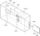
图17是示意性地图示根据本发明构思的实施例的
图18是示意性地图示根据本发明构思的实施例的通信设备的框图。FIG. 18 is a block diagram schematically illustrating a communication device according to an embodiment of the inventive concept.
图19是示意性地图示应用根据本发明构思的实施例的数据存储设备的系统的图。FIG. 19 is a diagram schematically illustrating a system applying a data storage device according to an embodiment of the inventive concept.
图20是示意性地图示根据本发明构思的实施例的存储卡的框图。FIG. 20 is a block diagram schematically illustrating a memory card according to an embodiment of the inventive concept.
图21是示意性地图示根据本发明构思的实施例的数字照相机的框图。FIG. 21 is a block diagram schematically illustrating a digital camera according to an embodiment of the inventive concept.
图22是示意性地图示应用图21中的存储卡的各种系统的图。FIG. 22 is a diagram schematically illustrating various systems to which the memory card in FIG. 21 is applied.
具体实施方式Detailed ways
将参考附图详细描述实施例。然而,本发明构思可以按各种不同的形式来实施,而不应被解释为仅限于例示的实施例。相反,提供这些实施例作为示例以使得本公开将是全面的和完整的,并将向本领域技术人员充分地传达本发明构思的构思。因此,关于本发明构思的某些实施例,不描述已知的处理、元件和技术。除非另外指出,否则相同的参考数字贯穿附图和文字描述指示相同的元件,并且因此将不重复描述。在附图中,为了清楚起见,层与区域的尺寸和相对尺寸可能被放大。Embodiments will be described in detail with reference to the accompanying drawings. However, the inventive concept can be implemented in various forms and should not be construed as limited to the illustrated embodiments. Rather, these embodiments are provided as examples so that this disclosure will be thorough and complete, and will fully convey the concept of the inventive concept to those skilled in the art. Accordingly, known processes, elements and techniques are not described with respect to certain embodiments of the inventive concepts. Unless otherwise indicated, the same reference numerals designate the same elements throughout the drawings and written description, and thus description will not be repeated. In the drawings, the size and relative sizes of layers and regions may be exaggerated for clarity.
将会理解,尽管术语“第一”、“第二”、“第三”等可以在此处用来描述各个元件、组件、区域、层和/或部分,但是这些元件、组件、区域、层和/或部分不应当被这些术语限制。这些术语仅用来将一个元件、组件、区域、层或部分与另一个区域、层或部分相区分。因此,下面讨论的第一元件、组件、区域、层或部分可以被称作第二元件、组件、区域、层或部分,而不会背离本发明构思的教导。It will be understood that although the terms "first", "second", "third" etc. may be used herein to describe various elements, components, regions, layers and/or sections, these elements, components, regions, layers and/or parts should not be limited by these terms. These terms are only used to distinguish one element, component, region, layer or section from another region, layer or section. Thus, a first element, component, region, layer or section discussed below could be termed a second element, component, region, layer or section without departing from the teachings of the present inventive concept.
为了易于描述,这里可以使用空间相对术语,诸如“在...之下”、“下面”、“下”、“之下”、“上面”、“上”等等,以描述如附图中图示的一个元件或特征与另一个或多个元件或特征的关系。将会理解,空间相对术语意图涵盖除了附图中描述的方向之外的使用中或操作中的设备的不同的方向。例如,如果附图中的设备被翻转,则被描述为在其他元件或特征“下面”或“下方”或“之下”的元件将在该其他元件或特征“上面”。因此,示例性术语“下面”和“之下”可以涵盖上面和下面两个方向。设备可以另外地定向(旋转90度或在其他方向),并相应地解释这里使用的空间相对描述词。此外,还将理解,当层被称为在两层“之间”时,其可以是两层之间仅有的层,或也可以存在一个或多个居间层。For ease of description, spatially relative terms may be used herein, such as "below", "under", "below", "below", "above", "on" and so on, to describe The relationship of one element or feature to another element or features is illustrated. It will be understood that the spatially relative terms are intended to encompass different orientations of the device in use or operation in addition to the orientation depicted in the figures. For example, if the device in the figures is turned over, elements described as "below" or "beneath" or "beneath" other elements or features would then be oriented "above" the other elements or features. Thus, the exemplary terms "below" and "under" can encompass both an orientation of above and below. The device may be otherwise oriented (rotated 90 degrees or at other orientations) and the spatially relative descriptors used herein interpreted accordingly. In addition, it will also be understood that when a layer is referred to as being "between" two layers, it can be the only layer between the two layers, or one or more intervening layers may also be present.
这里使用的术语仅仅用于描述特定实施例的目的,而不意欲限制本发明构思。如这里使用的,单数形式“一”意欲也包括复数形式,除非上下文另外地明确指示出。还将理解,当在该说明书中使用时,术语“包括”指明所声明的特征、整体、步骤、操作、元件和/或组件的存在,但是不排除存在或添加一个或多个其他特征、整体、步骤、操作、元件、组件和/或它们的组。如这里使用的,术语“和/或”包括相关联的列出项中的任意一个以及一个或多个的所有组合。同样,术语“示例性”意欲指示示例或例示。The terminology used herein is for the purpose of describing particular embodiments only and is not intended to limit the inventive concept. As used herein, the singular form "a" and "an" is intended to include the plural forms as well, unless the context clearly dictates otherwise. It will also be understood that when used in this specification, the term "comprising" indicates the presence of stated features, integers, steps, operations, elements and/or components, but does not exclude the presence or addition of one or more other features, integers , steps, operations, elements, components and/or groups thereof. As used herein, the term "and/or" includes any one and all combinations of one or more of the associated listed items. Likewise, the term "exemplary" is intended to mean an example or illustration.
将理解,当元件或层被称为“在…上”、“连接到”、“耦接到”或“相邻于”另一个元件或层时,它可以直接在该另一个元件或层上、直接连接到、直接耦接到或紧邻于其他元件或层,或可以存在居间的元件或层。相反,当元件被称为直接在另一个元件或层上或“直接连接到”、“直接耦接到”或“紧邻于”另一个元件或层时,不存在居间的元件或层。It will be understood that when an element or layer is referred to as being "on," "connected to," "coupled to," or "adjacent to" another element or layer, it can be directly on the other element or layer , directly connected to, directly coupled to, or immediately adjacent to other elements or layers, or intervening elements or layers may be present. In contrast, when an element is referred to as being directly on, "directly connected to," "directly coupled to" or "directly adjacent to" another element or layer, there are no intervening elements or layers present.
除非另外限定,否则在此使用的所有术语(包括科学数据和技术术语)具有与本发明构思所属领域的普通技术人员通常理解的相同含义。还将理解,诸如在通常使用的词典中所限定的那些术语应当被解释为具有与它们在相关领域和/或本说明书的上下文中的含义一致的含义,并且将不以理想化的或过度形式化的意义来解释,除非在此明确地如此定义。Unless otherwise defined, all terms (including scientific data and technical terms) used herein have the same meaning as commonly understood by one of ordinary skill in the art to which this inventive concept belongs. It will also be understood that terms such as those defined in commonly used dictionaries should be interpreted to have a meaning consistent with their meaning in the relevant field and/or in the context of this specification, and will not be in an idealized or excessive form. shall be construed in a defined sense unless expressly so defined herein.
随着在每个存储单元中存储的数据位的数量增加(或对应于每条字线的页(或页数据)的数量增加),已经提出了各种编程技术。例如,片上缓冲编程方法可以应用于包括多位存储器件的存储器系统。通过使用片上缓冲编程方法可以减小在存储器系统的存储器控制器中包括的缓冲存储器的尺寸。片上缓冲编程方法可以包括在多位存储器件的第一存储区域编程在存储器控制器的缓冲存储器临时存储的数据,以及在多位存储器件的第二存储区域编程在多位存储器件的第一存储区域存储的数据。在多位存储器件的第一存储区域编程在缓冲存储器临时存储的数据可以称为缓冲编程操作,在多位存储器件的第二存储区域编程在多位存储器件的第一存储区域存储的数据可以称为主编程操作。也就是说,片上缓冲编程方法可以包括缓冲编程操作和主编程操作。多位存储器件还可以包括除了第一存储区域和第二存储区域以外的其他存储区域。As the number of data bits stored in each memory cell increases (or the number of pages (or page data) corresponding to each word line increases), various programming techniques have been proposed. For example, the on-chip buffer programming method can be applied to a memory system including multi-bit memory devices. The size of a buffer memory included in a memory controller of a memory system can be reduced by using an on-chip buffer programming method. The on-chip buffer programming method may include programming data temporarily stored in a buffer memory of a memory controller in a first storage area of the multi-bit storage device, and programming the first storage area of the multi-bit storage device in a second storage area of the multi-bit storage device. The data stored by the region. Programming the data temporarily stored in the buffer memory in the first storage area of the multi-bit storage device may be referred to as a buffer programming operation, and programming the data stored in the first storage area of the multi-bit storage device in the second storage area of the multi-bit storage device may be Called the main programming operation. That is, the on-chip buffer program method may include a buffer program operation and a main program operation. The multi-bit memory device may also include other memory areas than the first memory area and the second memory area.
在示例实施例中,当与第一存储区域的最小编程单位对应的数据聚集在存储器控制器的缓冲存储器处时,可以执行缓冲编程操作。当对应于第二存储区域的最小编程单位的数据聚集在多位存储器件的第一存储区域时,或者当第一存储区域的可用存储空间不足时,可以执行主编程操作。此处,对应于第一存储区域的最小编程单位的数据可以是一页数据,对应于第二存储区域的最小编程单位的数据可以是多页数据。构成多页的页的数量可以根据每单元位数来决定。例如,在每单元位数为3(即,在每个单元中存储3位数据)的情况中,对应于第二存储区域的最小编程单位的数据可以是3页数据。可以理解,第一存储区域和第二存储区域的最小编程单位不限于该公开。关于上面的描述,每当对应于第一存储区域的最小编程单位的数据聚集在缓冲存储器处时,可以在多位存储器件的第一存储区域编程缓冲存储器的数据。因此,可以减小缓冲存储器的尺寸。In example embodiments, the buffer program operation may be performed when data corresponding to the minimum program unit of the first storage area is accumulated at the buffer memory of the memory controller. The main program operation may be performed when data corresponding to a minimum program unit of the second storage area is gathered in the first storage area of the multi-bit memory device, or when an available storage space of the first storage area is insufficient. Here, the data corresponding to the minimum programming unit of the first storage area may be one page of data, and the data corresponding to the minimum programming unit of the second storage area may be multiple pages of data. The number of pages constituting a plurality of pages can be determined in terms of bits per unit. For example, in case the number of bits per cell is 3 (ie, 3 bits of data are stored in each cell), the data corresponding to the minimum programming unit of the second storage area may be 3 pages of data. It can be understood that the minimum programming unit of the first storage area and the second storage area is not limited to this disclosure. Regarding the above description, whenever data corresponding to the minimum program unit of the first storage area is gathered at the buffer memory, data of the buffer memory may be programmed at the first storage area of the multi-bit memory device. Therefore, the size of the buffer memory can be reduced.
在采用片上缓冲编程方法的存储器系统中,主编程操作可以使用各种编程技术来进行。例如,主编程操作可以根据重编程技术来执行。下面,将参考图1更充分地描述使用重编程技术的主编程操作。In a memory system employing an on-chip buffer programming method, a main programming operation can be performed using various programming techniques. For example, a main program operation may be performed according to a reprogramming technique. Hereinafter, a main program operation using a reprogramming technique will be more fully described with reference to FIG. 1 .
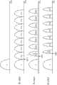
图1是示意性地图示根据本发明构思的实施例的根据重编程技术执行的编程操作的图。参见图1,图示了其中根据重编程技术编程3位数据(或由最低有效位(LSB)页数据、中央有效位(CSB)页数据和最高有效位(MSB)页数据形成的3页数据)的示例。然而,3位数据仅作为示例而给出,并且重编程技术不限于3位数据。FIG. 1 is a diagram schematically illustrating a program operation performed according to a reprogramming technique, according to an embodiment of the inventive concept. See Figure 1, which illustrates where 3-bit data (or 3-page data formed by Least Significant Bit (LSB) page data, Center Significant Bit (CSB) page data, and Most Significant Bit (MSB) page data) is programmed according to the reprogramming technique ) example. However, 3-bit data is given only as an example, and the reprogramming technique is not limited to 3-bit data.
在图1的示例中,重编程技术可以包括将充分描述的第一编程、第二编程和第三编程。In the example of FIG. 1, the reprogramming technique may include first programming, second programming, and third programming as will be fully described.
在第一编程,各个存储单元可以保持在擦除状态E或者被从擦除状态E编程到编程状态E和P11到P17中的一种。这里,如图1所图示的,8种状态E和P11到P17可以彼此相邻并且在其间没有读取余量(read margin)。也就是说,可以认为3位数据在第一编程被粗略的编程。所述3位数据可以经由缓冲编程操作在第一存储区域编程,并可以在第一编程从第一存储区域读取。In the first programming, each memory cell may remain in the erased state E or be programmed from the erased state E to one of the programmed state E and P11 to P17. Here, as illustrated in FIG. 1 , the 8 states E and P11 to P17 may be adjacent to each other without a read margin therebetween. That is, it can be considered that 3-bit data is roughly programmed in the first programming. The 3-bit data may be programmed in the first memory area via a buffer program operation, and may be read from the first memory area in the first program.
在示例实施例中,可以按照增量步进脉冲编程(ISPP)技术来执行第一编程,在所述ISPP技术中编程电压在编程循环的每个迭代递增。In example embodiments, the first programming may be performed according to an incremental step pulse programming (ISPP) technique in which the programming voltage is incremented at each iteration of the programming loop.
在示例实施例中,第一编程可以包括验证操作。在第一编程的验证操作中,可以验证至少一个编程状态。例如,在第一编程中,可以验证偶数编程状态P12、P14和P16,并且可以不验证奇数编程状态P11、P13、P15和P17。换句话说,在该示例中,在编程状态P12、P14和P16通过验证时,第一编程可以完成。In example embodiments, the first programming may include a verify operation. In the verify operation of the first program, at least one program state may be verified. For example, in the first programming, even program states P12, P14, and P16 may be verified, and odd program states P11, P13, P15, and P17 may not be verified. In other words, in this example, when program states P12, P14, and P16 pass verify, the first program can be completed.
可以执行第二编程以重编程在第一编程中编程的3位数据,即,将第一编程的状态P11到P17重编程到具有更高密度的阈值电压分布的状态P21到P27。这里,如图1所示,状态P21到P27可以彼此相邻并且在其间插入预定的读取余量。如上所述,在第二编程中使用的3位数据可以与在第一编程中使用的相同,并且可以从第一存储区域读取。如图1所示,第一编程的状态P11可以被重编程到第二编程的状态P21。结果,与状态P21对应的阈值电压分布可以在宽度上变得比与状态P11对应的阈值电压分布更窄。换句话说,用于验证第二编程的状态P21的验证电压VR21可以高于用于验证第一编程的状态P11的验证电压VR11。The second programming may be performed to reprogram the 3-bit data programmed in the first programming, that is, reprogram the states P11 to P17 of the first programming to the states P21 to P27 having a higher density threshold voltage distribution. Here, as shown in FIG. 1 , the states P21 to P27 may be adjacent to each other with a predetermined read margin interposed therebetween. As described above, the 3-bit data used in the second programming may be the same as that used in the first programming, and may be read from the first storage area. As shown in FIG. 1, the first programmed state P11 may be reprogrammed to the second programmed state P21. As a result, the threshold voltage distribution corresponding to the state P21 can become narrower in width than the threshold voltage distribution corresponding to the state P11. In other words, the verification voltage VR21 for verifying the second programmed state P21 may be higher than the verification voltage VR11 for verifying the first programmed state P11.
在示例实施例中,第二编程可以根据ISPP技术来执行。In example embodiments, the second programming may be performed according to ISPP technology.
在示例实施例中,第二编程可以包括验证操作。在第二编程的验证操作可以验证所有的编程状态。也就是说,在所有的编程状态P21到P27通过验证时,第二编程可以完成。In example embodiments, the second programming may include a verify operation. The verify operation in the second program can verify all the programmed states. That is, when all the program states P21 to P27 pass verification, the second program may be completed.
可以执行第三编程以重编程在第二编程编程的3位数据,即,将第二编程的状态P21到P27重编程为更密集的状态P31到P37。这里,如图1所示,状态P31到P37可以彼此相邻并且具有在其间插入的比第二编程的预定读取余量更大的预定读取余量。如上所述,在第三编程使用的3位数据可以等于在第一/第二编程使用的3位数据,并且可以从第一存储区域读取。在执行第三编程时,第二编程的状态P21可以被重编程到第三编程的状态P31。结果,与第三编程的状态P31对应的阈值电压分布可以在宽度上比与第二编程的状态P21对应的阈值电压分布更窄。换句话说,用于验证第三编程的状态P31的验证电压VR31可以高于用于验证第二编程的状态P21的验证电压VR21。The third programming may be performed to reprogram the 3-bit data programmed in the second programming, ie, reprogram the states P21 to P27 of the second programming into denser states P31 to P37. Here, as shown in FIG. 1 , the states P31 to P37 may be adjacent to each other with a predetermined read margin greater than that of the second program interposed therebetween. As described above, 3-bit data used in the third program may be equal to 3-bit data used in the first/second program, and may be read from the first storage area. When the third programming is performed, the second programmed state P21 may be reprogrammed to the third programmed state P31. As a result, the threshold voltage distribution corresponding to the third programmed state P31 may be narrower in width than the threshold voltage distribution corresponding to the second programmed state P21. In other words, the verification voltage VR31 for verifying the third programmed state P31 may be higher than the verification voltage VR21 for verifying the second programmed state P21.
在示例实施例中,第三编程可以根据ISPP技术来执行。In example embodiments, the third programming may be performed according to ISPP technology.
在示例实施例中,在第三编程的验证操作可以验证所有的编程状态。也就是说,在所有的编程状态P31到P37通过验证时,第三编程可以完成。In example embodiments, the verify operation at the third program may verify all program states. That is, when all the program states P31 to P37 pass verification, the third program can be completed.
如前所述,本发明构思不限于在第一编程编程3位数据的示例。本发明构思可以应用于其中在第一编程编程2位数据的示例。在对2位数据第一编程之后,可以执行第二编程以编程1位数据。然后,可以执行第三编程以获得目标阈值电压分布。相关的编程技术在美国专利公开文件第2011-0222342号中公开,其整体内容通过引用合并于此。As mentioned earlier, the inventive concept is not limited to the example of programming 3-bit data in the first program. The inventive concept may be applied to an example in which 2-bit data is programmed in the first program. After first programming 2-bit data, second programming may be performed to program 1-bit data. Then, a third programming may be performed to obtain the target threshold voltage distribution. Related programming techniques are disclosed in US Patent Publication No. 2011-0222342, the entire contents of which are hereby incorporated by reference.
图1所示的3位编程操作可以以3步编程技术来进行。然而,本发明构思不限于此。在本发明构思中,在重编程技术中执行的编程操作可以包括3个编程操作,该3个编程操作被执行以使得与要存储的数据值对应的阈值电压分布变窄(换句话说,精细地形成阈值电压分布)。The 3-bit programming operation shown in FIG. 1 can be performed in a 3-step programming technique. However, the inventive concept is not limited thereto. In the present inventive concept, the program operation performed in the reprogramming technique may include 3 program operations performed such that the threshold voltage distribution corresponding to the data value to be stored is narrowed (in other words, finely tuned). ground to form a threshold voltage distribution).
图2是示意性地图示根据本发明构思的实施例的存储器系统的框图。FIG. 2 is a block diagram schematically illustrating a memory system according to an embodiment of the inventive concept.
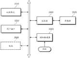
参见图2,根据本发明构思的实施例的存储器系统1000可以包括存储器控制器1200和作为多位存储器件的非易失性存储器件1400。存储器控制器1200可以配置为根据外部请求(例如写入请求、读取请求等等)来控制非易失性存储器件1400。存储器控制器1200可以配置为无需外部请求、根据内部请求(例如与突然断电、损耗均衡操作、读取回收操作等相关联的操作)来控制非易失性存储器件1400。与存储器控制器1200的内部请求对应的操作可以在处理了主机请求之后、在主机的超时(timeout)时段内执行。可替换的,与存储器控制器1200的内部请求对应的操作可以在存储器控制器1200的空闲时间内执行。非易失性存储器件1400可以响应于存储器控制器1200的控制而操作,并且可以用作存储数据信息的一种存储介质。存储介质可以由一个或多个存储芯片形成。非易失性存储器件1400可以经由一个或多个通道与存储器控制器1200通信。非易失性存储器件1400可以包括例如NAND闪存设备。Referring to FIG. 2 , a
存储器系统1000可以使用上述片上缓冲编程技术。如下面将要描述的,非易失性存储器件1400可以包括具有第一存储区域和第二存储区域的存储单元阵列。在示例实施例中,第一存储区域的每单元位数可以少于第二存储区域的每单元位数。例如,第一存储区域可以由每单元存储1位数据的存储块形成,第二存储区域可以由每单元存储3位数据的存储块形成。然而,第一存储区域和第二存储区域中的每个的每单元位数不限于该示例。存储器控制器1200可以根据从第二存储区域中的存储块之一读取的数据的错误位数是否超过基准来执行读取回收操作。利用本发明构思的读取回收操作,存储在第二存储区域中的存储块处的数据可以被移动到第一存储区域中的存储块,但不能被移动到第二存储区域中的存储块。在本发明构思的情况中,当存储在第二存储区域中的存储块处的数据被移动到第一存储区域中的存储块时,与第二存储区域中的存储块相关联的读取回收操作可以结束。这将在下面更充分地描述。
图3是示意性地图示图2中示出的存储器控制器的示例的框图。参见图3,存储器控制器1200可以包括作为第一接口的主机接口1210、作为第二接口的存储器接口1220、CPU1230、缓冲存储器1240、以及错误检测和校正电路(ECC)1250。FIG. 3 is a block diagram schematically illustrating an example of the memory controller shown in FIG. 2 . Referring to FIG. 3 , the
主机接口1210可以配置为与外部设备(例如主机)接口连接,并且存储器接口1220可以配置为与图2图示的非易失性存储器件1400接口连接。CPU1230可以配置为控制控制器1200的整体操作。例如,CPU1230可以配置为操作诸如快闪转换层(FTL)的固件。FTL可以执行各种功能。例如,FTL可以包括进行地址映射操作、读取回收操作、错误校正操作等的各种层。缓冲存储器1240可以用于临时存储将经由主机接口1210从外部设备传送的数据或将经由存储器接口1220从非易失性存储器件1400传送的数据。缓冲存储器1240可以用于存储控制非易失性存储器件1400所需的信息(例如,指示读取回收操作需要的源存储块的信息、地址映射信息等)。The
缓冲存储器1240可以由DRAM、SRAM或DRAM和SRAM的组合形成。然而,本发明构思不限于此。ECC1250可以配置为编码将要存储在非易失性存储器件1400中的数据以及解码从非易失性存储器件1400读出的数据。The
尽管未在图中示出,存储器控制器1200还可以包括随机发生器/解随机发生器,该随机发生器/解随机发生器配置用来随机化将要存储在非易失性存储器件1400中的数据和解随机化从非易失性存储器件1400读出的数据。随机发生器/解随机发生器的示例在美国专利公开文件第2010/0088574号中公开,其全部内容通过引用合并于此。Although not shown in the figure, the
在示例实施例中,主机接口1210可以由计算机总线标准、存储总线标准和iFCPPeripheral总线标准中的一个形成,或者由两个或更多个标准的组合形成。计算机总线标准可以包括S-100总线、Mbus、Smbus、Q-Bus、ISA、ZorroII、Zorro III、CAMAC、FASTBUS、LPC、EISA、VME、VXI、NuBus、TURBOchannel、MCA、Sbus、VLB、PCI、PXI、HP GSC总线、CoreConnect、InfiniBand、UPA、PCI-X、AGP、PCIe、因特尔快速路径互连(Intel QuickPathInterconnect)、超传送(Hyper Transport),等等。存储总线标准可以包括ST-506、ESDI、SMD、并行ATA、DMA、SSA、HIPPI、USB MSC、火线(1394)、串行ATA、eSATA、SCSI、并行SCSI、串行附接SCSI(Serial Attached SCSI)、光纤通道、iSCSI、SAS、RapidIO、FCIP,等等。iFCPPeripheral总线标准可以包括苹果桌面总线、HIL、MIDI、多总线(Multibus)、RS-232、DMX512-A、EIA/RS-422、IEEE-1284、UNI/O、1-Wire、I2C、SPI、EIA/RS-485、USB、照相机链接(Camera Link)、外部PCIe、光峰(Light Peak)、多点总线(MultidropBus),等等。In example embodiments, the
图4是示意性地图示图2中示出的非易失性存储器件的示例的框图。FIG. 4 is a block diagram schematically illustrating an example of the nonvolatile memory device shown in FIG. 2 .
非易失性存储器件1400可以是例如NAND闪存器件。但是,能够理解,非易失性存储器件1400不限于NAND闪存器件。例如,本发明构思可以应用于NOR闪存器件、阻变随机存取存储器(RRAM)器件、相变存储器(PRAM)器件、磁阻随机存取存储器(MRAM)器件、铁电随机存取存储器(FRAM)器件、自旋转移力矩随机存取存储器(STT-RAM)等。此外,非易失性存储器件1400可以被实现为具有三维阵列结构。具有三维阵列结构的非易失性存储器件的示例可以称为垂直NAND闪存器件。本发明构思可以应用于包括由绝缘膜形成的电荷存储层的电荷捕获闪存(CTF)器件以及包括由导电浮置栅极形成的电荷存储层的闪存器件。The
参见图4,非易失性存储器件1400可以包括存储单元阵列1400、地址解码器1420、电压产生器1430、控制逻辑1440、页缓冲器电路1450和输入/输出接口1460。Referring to FIG. 4 , a
存储单元阵列1410可以包括布置在行(例如字线)和列(例如位线)的交叉处的存储单元。作为示例,每个存储单元可以存储1位数据或作为多位数据的m位数据(m是2或更大的整数)。地址解码器1420可以通过控制逻辑1440来控制,并且可以对存储单元阵列1410的行(例如字线、(一条或多条)串选择线、(一条或多条)地选择线、公共源极线等)进行选择和驱动操作。电压产生器1430可以由控制逻辑1440控制,并且可以产生每个操作需要的电压,诸如高电压、编程电压、读取电压、验证电压、擦除电压、通过电压、体(bulk)电压等。由电压产生器1430产生的电压可以经由地址解码器1420提供到存储单元阵列1410。控制逻辑1440可以配置为控制非易失性存储器件1400的整体操作。The
页缓冲器电路1450可以由控制逻辑1440控制,并且可以配置为从存储单元阵列1410读取数据并根据编程数据驱动存储单元阵列1410的列(例如位线)。页缓冲器电路1450可以包括分别对应于位线或位线对的页缓冲器。每个页缓冲器可以包括多个锁存器。输入/输出接口1460可以由控制逻辑1440控制,并且可以与外部设备(例如图2中的存储器控制器)接口连接。尽管图4中未示出,但是输入/输出接口1460可以包括列解码器,该列解码器配置用于选择预定单位的页缓冲器电路1450的页缓冲器、接收数据的输入缓冲器、输出数据的输出缓冲器等The
图5是示意性地图示图4中示出的存储单元阵列的示例的框图。FIG. 5 is a block diagram schematically illustrating an example of the memory cell array shown in FIG. 4 .
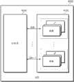
参见图5,存储单元阵列1410可以包括被划分到第一存储区域1411和第二存储区域1412中的多个存储块。这里,第一存储区域1411和第二存储区域1412的划分可以是逻辑地进行的,而不是物理地进行的。另外,第一存储区域1411和第二存储区域1412的划分可以逻辑地改变。换句话说,第一存储区域1411和第二存储区域1412的物理尺寸可以在存储器控制器1200的控制下逻辑地改变。第一存储区域1411由每单元存储n位数据的存储块形成,第二存储区域1412由每单元存储m位数据的存储块形成,其中n和m是整数。另外,第一存储区域1411中的存储块可以以与第二存储区域1412中的存储块不同的方式被编程,例如,n可以小于m。例如,第一存储区域1411中的存储块可以根据单个位编程技术(以下称为SLC编程技术)来编程,而第二存储区域1412中的存储块可以根据多位编程技术(以下称为MLC/TLC编程技术)(例如,上述的3步重编程技术)来编程。换句话说,第一存储区域1411中的每个存储单元可以存储1位数据(n=1),而第二存储区域1412中的每个存储单元可以存储m位数据(m是2或更大的整数)。在第一存储区域1411中的每个存储单元存储的数据位数可以比在第二存储区域1412中的每个存储单元存储的数据位数要少。此处,能够理解在第一存储区域1411中的每个存储单元不限于存储1位数据。Referring to FIG. 5 , a
如上所述,从存储器控制器1200提供的数据可以经由缓冲编程操作在第一存储区域1411被编程。用于主编程操作的数据可以从第一存储区域1411读出,并且所读取的数据可以经由主编程操作在第二存储区域1412被编程。As described above, data provided from the
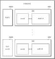
图6A到6D是用于描述根据本发明构思的实施例的多位存储器件的第一存储区域和第二存储区域的各种结合的图。在图中,“BP”指示第一存储区域1411上的缓冲编程,“MP”指示第二存储区域1412上的主编程。6A to 6D are diagrams for describing various combinations of first and second storage regions of a multi-bit memory device according to an embodiment of the inventive concept. In the drawing, 'BP' indicates buffer programming on the
如上所述,多位存储器件1400包括第一存储区域1411和第二存储区域1412。这里,第一存储区域1411和第二存储区域1412可以组成多位存储器件1400的存储单元阵列。尽管在图中未示出,存储单元阵列还可以包括诸如元区域、保留区域等的区域。能够理解,存储单元阵列的区域可以逻辑地划分,而不是物理地划分。这意味着存储单元阵列的所述区域可以根据存储器控制器1200的地址映射来定义。As described above, the
参见图6A,在每单元存储3位数据的多位存储器件的情况中,第一存储区域1411可以由每个存储1位数据的存储单元形成,第二存储区域1412可以由每个存储3位数据的存储单元形成。在该情况中,缓冲编程可以根据SLC编程技术来执行,主编程可以根据上述MLC编程技术来进行。Referring to FIG. 6A, in the case of a multi-bit memory device that stores 3-bit data per cell, the
参见图6B,在每单元存储4位数据的多位存储器件的情况中,第一存储区域1411可以由每个存储1位数据的存储单元形成,第二存储区域1412可以由每个存储4位数据的存储单元形成。在该情况中,缓冲编程可以根据SLC编程技术来执行,主编程可以根据上述MLC/TLC编程技术来进行。Referring to FIG. 6B , in the case of a multi-bit memory device storing 4-bit data per cell, the
参见图6C,在每单元存储3位数据的多位存储器件的情况中,第一存储区域1411可以由每个存储2位数据的存储单元形成,第二存储区域1412可以由每个存储3位数据的存储单元形成。在该情况中,缓冲编程可以根据上述或传统的MLC编程技术来执行,主编程可以根据上述MLC/TLC编程技术(例如,重编程技术)来进行。Referring to FIG. 6C, in the case of a multi-bit memory device storing 3-bit data per cell, the
参见图6D,在每单元存储4位数据的多位存储器件的情况中,第一存储区域1411可以由每个存储2位数据的存储单元形成,第二存储区域1412可以由每个存储4位数据的存储单元形成。在该情况中,缓冲编程可以根据上述或传统的MLC编程技术来执行,主编程可以根据上述MLC/TLC编程技术(例如,重编程技术)来进行。Referring to FIG. 6D , in the case of a multi-bit memory device storing 4-bit data per cell, the
在示例性实施例中,能够理解,图6A到6D中图示的第一存储区域1411和第二存储区域1412的定义不限于那些示例。例如,如果在存储器系统中包括的存储介质由多个多位存储器件形成,则可以关于各个多位存储器件来定义第一存储区域1411和第二存储区域1412。可替换的,一个或多个多位存储器的每个存储单元阵列可以定义为第一存储区域1411。剩余的多位存储器件的每个存储单元阵列可以定义为第二存储区域1412。In an exemplary embodiment, it can be understood that the definitions of the
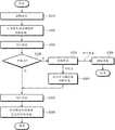
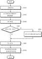
图7是图示根据本发明构思的实施例的存储器系统的读取方法的流程图。在下面的描述中,给出如下示例,其中第一存储区域1411由每单元存储1位数据的存储块(以下称为SLC块)形成,第二存储区域1412由每单元存储3位数据的存储块(以下称为TLC块)形成。FIG. 7 is a flowchart illustrating a reading method of a memory system according to an embodiment of the inventive concept. In the following description, an example is given in which the
参见图3、6A和7,在操作S110,存储器控制器1200可以从外部设备(例如主机)接收读取请求。在操作S120,存储器控制器1200可以控制非易失性存储器件1400,使得输出读取请求的数据。读取请求的数据可以是例如存储在第二存储区域1412的TLC块的数据。可替换的,读取请求的数据可以是存储在第一存储区域1411的SLC块的数据。在该实施例的示例中,读取请求的数据是存储在第二存储区域1412的TLC块的数据。Referring to FIGS. 3 , 6A and 7 , at operation S110 , the
在操作S130,当从非易失性存储器件1400输出的数据被传送到存储器控制器1200的缓冲存储器1240时,存储器控制器1200的ECC电路1250可以对从非易失性存储器件1400输出的数据进行错误检测操作。此时,从非易失性存储器件1400输出的数据可以临时存储在存储器控制器1200的缓冲存储器1240中。In operation S130, when the data output from the
在操作S140,可以确定在从非易失性存储器件1400输出的数据中包含的错误是否可以由ECC电路1250校正。如果该错误可以由ECC电路1250校正,则方法进行到操作S150。在操作S150,在从非易失性存储器件1400输出的数据中包含的错误可以由ECC电路1250校正,以获得校正的数据。在操作S160,校正的数据可以存储在缓冲存储器1240中并发送到外部设备作为读取请求的数据。此时,读取操作可以终止。In operation S140 , it may be determined whether an error contained in data output from the
返回到操作S140,例如,在从非易失性存储器件1400输出的数据的错误位数超过阈值(例如ECC电路1250的可允许错误位数)的情况中,可以认为从非易失性存储器件1400输出的数据中包含的错误不能被校正。在操作S140的不能校正的错误的情况下,方法进行到操作S170。在操作S170,存储器控制器1200可以使用软件对从非易失性存储器件1400输出的数据进行错误检测和校正操作。即,即使在从非易失性存储器件1400输出的数据中包括的错误位数超过ECC电路1250的可允许错误位数的情况中,也可以使用存储器控制器1200的错误检测和校正软件来校正从非易失性存储器件1400输出的数据中包含的错误。例如,错误检测和校正操作可以由快闪转换层(FTL)进行。在操作S180,可以确定从非易失性存储器件1400输出的数据是否已经在操作S170由软件校正。Returning to operation S140, for example, in the case where the number of error bits of the data output from the
如果确定从非易失性存储器件1400输出的数据不能由软件校正,则方法进行到操作S190。在操作S190,存储器控制器1200可以将由外部设备请求的读取操作处理为读取失败。例如,可以根据各种不同过程中的任何一种产生读取失败标记。此时,读取方法可以终止。If it is determined that the data output from the
另一方面,如果确定从非易失性存储器件1400输出的数据已经在操作S170由软件校正,则方法进行到操作S200。在操作S200,存储器控制器1200可以将在缓冲存储器1240存储的校正的数据发送到外部设备,作为读取请求的数据。此时,在CPU1230的控制下,可以在队列中存储指示存储读取请求的数据的TLC块是需要读取回收操作的存储块的信息。这里,这将在后面更充分地描述。On the other hand, if it is determined that the data output from the
在示例实施例中,所述队列可以由缓冲存储器1240的一部分形成,并且存储在队列中的信息可以被CPU1230引用。对于由于突然断电情况导致的队列信息的丢失,存储在队列中的信息还可以周期性地存储在非易失性存储器件1400中。对TLC块的读取回收操作可以基于存储在队列中的信息来执行。这里,这将在后面更充分地描述。In example embodiments, the queue may be formed by a part of the
图8A和8B是描述根据本发明构思的实施例的读取回收操作所参考的图。8A and 8B are diagrams referred to for describing a read reclaim operation according to an embodiment of the inventive concept.
由于各种原因,存储单元的阈值电压分布可能从理想的编程分布偏移。例如,温度的变化、多次读取操作迭代等可以使得阈值电压分布随时间而偏移。这一阈值电压分布的偏移可能导致读取数据中包含的错误位数据增加。在诸如每单元存储3位数据的TLC块的情况那样的读取余量较低的情况中尤其如此。即,在多位存储单元中由于阈值电压分布导致的错误位数可能进一步增加。由此,可以执行读取回收操作,以确保读取数据的完整性。读取回收操作是指将包括页数据的TLC块的有效数据移动到新块的操作。页数据可能被确定为是不可校正的,并且因此被移动到新块,或者页数据可能被确定为具有错误位数随后增加的高可能性,并且因此被移动到新块。可以由于存储页数据的存储单元的阈值电压分布的偏移影响相邻存储单元而执行读取回收操作。The threshold voltage distribution of memory cells may deviate from the ideal programming distribution for various reasons. For example, changes in temperature, multiple read operation iterations, etc. may cause the threshold voltage distribution to shift over time. This shift in threshold voltage distribution may lead to an increase in erroneous bit data contained in read data. This is especially true in cases where the read margin is low, such as the case of a TLC block storing 3 bits of data per cell. That is, the number of error bits due to threshold voltage distribution may further increase in a multi-bit memory cell. Thus, a read reclamation operation can be performed to ensure the integrity of the read data. A read reclamation operation refers to an operation of moving valid data of a TLC block including page data to a new block. The page data may be determined to be uncorrectable and thus moved to a new block, or the page data may be determined to have a high probability of a subsequent increase in the number of error bits and therefore be moved to a new block. The read reclamation operation may be performed due to a shift in threshold voltage distribution of memory cells storing page data affecting adjacent memory cells.
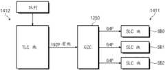
参见图8A,CPU1230可以基于存储在队列中的信息,选择作为快闪转换层FTL的读取回收操作的目标块的TLC块。例如,假设所选择的TLC块包括64条字线。因此,在每单元3位的存储器的情况下,192页数据可以存储在一个TLC块中。在存储在所选择的TLC块中的192页数据全部有效的情况下,可以需要三个SLC块来移动存储在所选择的TLC块的192页数据。可以从所选择的TLC块读取64页数据以执行读取回收操作,并且该64页读取的数据可以经由存储器控制器1200的ECC电路1250被存储在第一存储区域1411的一个SLC块SB0中。然后,可以从所选择的TLC块读取64页数据以用于读取回收操作,并且该64页读取数据可以经由存储器控制器1200的ECC电路1250而被存储在第一存储区域1411的一个SLC块SB1中。最后,可以从所选择的TLC块读取64页数据以用于读取回收操作,并且该64页读取的数据可以经由存储器控制器1200的ECC电路1250被存储在第一存储区域1411的一个SLC块SB2中。Referring to FIG. 8A , the
参见图8B,在存储在所选择的TLC块的192页数据的150页数据有效的情况下,可以需要3个SLC块来移动在所选择的TLC块存储的150页数据。可以从所选择的TLC块读取64页数据以执行读取回收操作,并且该64页读取的数据可以经由存储器控制器1200的ECC电路1250存储在第一存储区域1411的一个SLC块SB0中。然后,可以从所选择的TLC块读取64页数据以用于读取回收操作,并且该64页读取的数据可以经由存储器控制器1200的ECC电路1250存储在第一存储区域1411的一个SLC块SB1中。最后,可以从所选择的TLC块读取22页数据以用于读取回收操作,并且该22页读取的数据可以经由存储器控制器1200的ECC电路1250存储在第一存储区域1411的一个SLC块SB2中。Referring to FIG. 8B , in case 150 pages of data stored in the selected TLC block of 192 pages of data are valid, 3 SLC blocks may be required to move the 150 pages of data stored in the selected TLC block. 64 pages of data may be read from the selected TLC block to perform a read reclamation operation, and the 64 pages of read data may be stored in one SLC block SB0 of the
当存储在TLC块的所有有效页数据都被移动到第一存储区域1411时,CPU1230可以将对于TLC块的FTL的读取回收操作处理为完成。例如,可以改变存储在队列中的(指示读取回收操作的目标块的)信息。When all valid page data stored in the TLC block is moved to the
如上所述,利用本发明构思的读取回收操作,作为读取回收操作的目标块的TLC块的有效页数据可以被移动到第一存储区域1411的SLC块,而不是被移动到第二存储区域1412的TLC块。如果数据到第一存储区域1411的SLC块的传送完成,则对TLC块的读取回收操作可以被处理为完成。换句话说,在本发明构思的读取回收操作中,作为读取回收操作的目标块的TLC块的有效页数据不能被移动到第二存储区域1412的TLC块。As described above, with the read reclamation operation of the inventive concept, the valid page data of the TLC block which is the target block of the read reclamation operation can be moved to the SLC block of the
在示例实施例中,作为读取回收操作的目标块的TLC块的有效页数据可以以时分方式移动到第一存储区域1411的SLC块。例如,作为读取回收操作的目标块的TLC块的部分有效页数据(例如,对应于SLC块大小的有效页数据)可以被移动到一个SLC块。这可以在每次主机请求读取或写入操作时在读取或写入操作完成后的主机超时时段内执行。当TLC块的所有有效页数据都被移动到SLC块时,对TLC块的读取回收操作可以完成。In example embodiments, valid page data of a TLC block that is a target block of a read reclamation operation may be moved to an SLC block of the
在示例实施例中,作为读取回收操作的目标块的TLC块的有效页数据将要移动到的第一存储区域1411的SLC块的数量可以考虑主机超时时段来决定。例如,第一存储区域1411的SLC块的数量可以考虑在处理了主机的写入请求之后超时时段的剩余时间来决定。作为读取回收操作的目标块的TLC块的数据可以移动到在主机的写入请求决定的SLC块。In example embodiments, the number of SLC blocks of the
从TLC块移动到SLC块的数据可以经由主编程操作存储在第二存储区域1412中。这一操作可以在垃圾收集操作进行。这将参考图9更充分地描述。Data moved from the TLC block to the SLC block may be stored in the
如上所述,当TLC块的有效页数据被移动到第一存储区域1411的SLC块时,本发明构思的读取回收操作可以完成。根据TLC块的有效页的数量,SLC块之一可以包括空的存储空间。例如,参考图8B和9,在存储在所选择的TLC块的192页数据中的150页数据有效时,需要三个SLC块来移动存储在所选择的TLC块中的150页数据,并且一个SLC块(例如SB2)可以包括空的存储空间。在垃圾收集操作中,除了包括空的存储空间的SLC块SB2之外的其余SLC块SB0和SB1的数据可以和填满了数据的其他SLC块(例如SB3)的数据一起存储在特定的TLC块中。如果SLC块的数据以上述方式存储在TLC块中,则该TLC块可以被填满数据。换句话说,TLC块的所有字线可以关闭(close)。这可以意味着TLC块不包括打开(open)的字线。另一方面,如果存储所选择的TLC块所存储的150页数据的SLC块SB0、SB1和SB2的数据被存储在特定的TLC块中,则在该特定的TLC块中可以存在空的存储空间。这可以意味着该特定TLC块包括打开的字线。As described above, when the valid page data of the TLC block is moved to the SLC block of the
这里,在对与第n条字线WLn连接的存储单元的3步重编程完成、并且未执行对与相邻字线(例如WLn+1)连接的存储单元的3步重编程的第三编程的情况下,第n条字线WLn可以被称为打开的字线。当对与相邻的上部字线连接的存储单元的3步重编程完成时,可以形成与打开的字线连接的存储单元的目标阈值电压分布。如果对与相邻的上部字线连接的存储单元的3步重编程未完成,则与打开的字线连接的存储单元的目标阈值电压分布不能正常形成。例如,与打开的字线连接的存储单元可能不充分地经历由与相邻的上部字线连接的存储单元造成的耦合,从而与打开的字线连接的存储单元的目标阈值电压分布不正常形成。在该情况下,从与打开的字线连接的存储单元读取的数据不能校正的可能性会增大。Here, after the 3-step reprogramming of the memory cells connected to the n-th word line WLn is completed, and the third programming of the 3-step reprogramming of the memory cells connected to the adjacent word line (eg WLn+1) is not performed In the case of , the n-th word line WLn may be referred to as an turned-on word line. When the 3-step reprogramming of the memory cells connected to the adjacent upper word line is completed, the target threshold voltage distribution of the memory cells connected to the opened word line may be formed. If the 3-step reprogramming of the memory cells connected to the adjacent upper word line is not completed, the target threshold voltage distribution of the memory cells connected to the opened word line cannot be normally formed. For example, a memory cell connected to an open word line may not experience sufficient coupling caused by a memory cell connected to an adjacent upper word line such that the target threshold voltage distribution of the memory cell connected to the open word line does not form normally. . In this case, there is an increased possibility that data read from memory cells connected to the opened word line cannot be corrected.
因此,可以通过以下方式防止在特定的TLC块中存在打开的字线:在垃圾收集操作中,将除了包括空的存储空间的SLC块SB2之外的其余SLC块SB0和SB1的数据和填满了数据的另一个SLC块(例如SB3)的数据一起存储在该特定的TLC块中。Therefore, the presence of open word lines in a specific TLC block can be prevented by filling up the data sum of the remaining SLC blocks SB0 and SB1 in garbage collection operations except for the SLC block SB2 which includes empty memory space. Data from another SLC block (such as SB3) that has received data is stored in that particular TLC block.
在示例实施例中,可以将具有空的存储空间的SLC块(例如SB2)的数据移动到另一个SLC块中,或者可以将其和另一个具有空的存储空间的SLC块的数据一起移动到TLC块中。In an example embodiment, the data of an SLC block with empty storage space (such as SB2) can be moved to another SLC block, or it can be moved together with the data of another SLC block with empty storage space to TLC block.
图10是图示根据本发明构思的另一实施例的存储器系统的读取方法的流程图。下面,将参考附图更充分地描述根据本发明构思的实施例的存储器系统的读取方法。例如,假设第一存储区域1411由每单元存储1位数据的存储块(在下文中称为SLC块)形成,第二存储区域1412由每单元存储3位数据的存储块(在下文中称为TLC块)形成。FIG. 10 is a flowchart illustrating a read method of a memory system according to another embodiment of the inventive concept. Hereinafter, a reading method of a memory system according to an embodiment of the inventive concept will be more fully described with reference to the accompanying drawings. For example, assume that the
在操作S310,存储器控制器1200可以从外部设备(例如,主机)接收读取请求。在操作S320,存储器控制器1200可以控制非易失性存储器件1400,使得输出读取请求的数据。读取请求的数据可以是例如存储在第二存储区域1412的TLC块的数据。可替换地,读取请求的数据可以是存储在第一存储区域1411的SLC块的数据。在示例实施例中,读取请求的数据可以是存储在第二存储区域1412的TLC块的数据。In operation S310, the
在操作S330,当从非易失性存储器件1400输出的数据被传送到存储器控制器1200的缓冲存储器1240时,存储器控制器1200的ECC电路1250可以对从非易失性存储器件1400输出的数据进行错误检测操作。此时,从非易失性存储器件1400输出的数据可以临时存储在存储器控制器1200的缓冲存储器1240中。In operation S330, when the data output from the
在操作S340,可以确定从非易失性存储器件1400输出的数据的错误是否可校正。如果可校正,则方法进行到操作S350。在操作S350,从非易失性存储器件1400输出的数据的错误可以被校正。在操作S360,存储在缓冲存储器1240中的经校正的数据可以被发送到外部设备,以作为读取请求的数据。然后,读取操作可以终止。In operation S340, it may be determined whether an error of data output from the
返回到S340,如果从非易失性存储器件1400输出的数据不可校正或者在从非易失性存储器件1400输出的数据的错误位数超过基准(例如ECC电路1250的可允许错误位数)的情况下,方法进行到操作S370。在操作S370,可以进行读取重试操作。在读取重试操作,可以在预定数量内在读取电压变化的条件下重试读取操作。示例性读取重试操作在美国专利公开文件第2010/0322007号中公开,其整体内容通过引用合并于此。可以确定每当读取电压变化时读取的数据是否可校正。在经由读取重试操作读取的数据不可校正的情况下,方法继续到操作S380。在操作S380,可以产生读取失败标记。根据读取失败标记的产生的过程可以不同地确定。此后,方法可以结束。Returning to S340, if the data output from the
在经由读取重试操作读取的数据可校正的情况下,方法继续到操作390。在操作S390,可以在队列中存储指示存储从非易失性存储器件1400输出的数据的第二存储区域1412的TLC块是读取回收操作的目标块的信息。如上所述,所述队列可以由缓冲存储器1240的一部分形成,并且存储在队列中的信息可以被CPU1230引用。存储在队列中的信息可以周期性地或在预定的时间被存储到非易失性存储器件1400中。可以这样执行以防止存储在队列中的信息由于突然断电而丢失。对TLC块的读取回收操作可以基于存储在队列中的信息来进行,这里,其将在后面更充分地描述。In case the data read via the read retry operation is correctable, the method continues to operation 390 . In operation S390, information indicating that a TLC block of the
在指示存储从非易失性存储器件1400输出的数据的第二存储区域1412的TLC块是读取回收操作的目标块的信息被存储在队列中后,方法进行到操作S350。在操作S350,从非易失性存储器件1400输出的数据的错误可以被校正。在操作S360,存储在缓冲存储器1240中的经校正的数据可以作为读取请求的数据被发送到外部设备。此后,读取操作可以终止。After information indicating that a TLC block of the
存储器控制器1200可以基于存储在队列中的信息执行读取回收操作,其与参考图8A,8B和9所描述的相同地进行。The
图11是图示根据本发明构思的又一实施例的存储器系统的读取方法的流程图。下面,将参考附图更充分地描述根据本发明构思的实施例的存储器系统的读取方法。例如,假设第一存储区域1411由每单元存储1位数据的存储块(在下文中称为SLC块)形成,第二存储区域1412由每单元存储3位数据的存储块(在下文中称为TLC块)形成。FIG. 11 is a flowchart illustrating a reading method of a memory system according to still another embodiment of the inventive concept. Hereinafter, a reading method of a memory system according to an embodiment of the inventive concept will be more fully described with reference to the accompanying drawings. For example, assume that the
在操作S410,存储器控制器1200可以从外部设备(例如,主机)接收读取请求。在操作S420,存储器控制器1200可以控制非易失性存储器件1400,使得输出读取请求的数据。读取请求的数据可以是例如存储在第二存储区域1412的TLC块的数据。可替换地,读取请求的数据可以是存储在第一存储区域1411的SLC块的数据。在示例实施例中,读取请求的数据可以是存储在第二存储区域1412的TLC块的数据。In operation S410, the
在操作S430,当从非易失性存储器件1400输出的数据被传送到存储器控制器1200的缓冲存储器1240时,存储器控制器1200的ECC电路1250可以对从非易失性存储器件1400输出的数据进行错误检测操作。此时,从非易失性存储器件1400输出的数据可以临时存储在存储器控制器1200的缓冲存储器1240中。In operation S430, when the data output from the
在操作S440,可以确定从非易失性存储器件1400输出的数据中包括的错误位数是否低于基准。这里,所述基准可以是ECC电路1250的可允许错误位数、少于可允许错误位数的错误位数,等等。如果从非易失性存储器件1400输出的数据中包括的错误位数超过基准,则方法进行到操作S450。在操作S450,可以在队列中存储指示存储从非易失性存储器件1400输出的数据的第二存储区域1412的TLC块是读取回收操作的目标块的信息。如上所述,所述队列可以由缓冲存储器1240的一部分形成,并且存储在队列中的信息可以被CPU1230引用。存储在队列中的信息可以周期性地或在预定的时间被存储到非易失性存储器件1400中。可以这样执行以防止存储在队列中的信息由于突然断电而丢失。对TLC块的读取回收操作可以基于存储在队列中的信息来进行,其将在后面更充分地描述。In operation S440, it may be determined whether the number of error bits included in the data output from the
在指示存储从非易失性存储器件1400输出的数据的第二存储区域1412的TLC块是读取回收操作的目标块的信息被存储在队列中后,方法进行到操作S460。在操作S460,从非易失性存储器件1400输出的数据的错误可以被校正。在操作S470,存储在缓冲存储器1240中的经校正的数据可以被发送到外部设备以作为读取请求的数据。此后,读取操作可以终止。After information indicating that a TLC block of the
存储器控制器1200可以基于存储在队列中的信息执行读取回收操作,其与参考图8A,8B和9所描述的相同地进行。The
图12是示意性地图示根据本发明构思的实施例的存储器系统的读取回收技术的框图。FIG. 12 is a block diagram schematically illustrating a read reclamation technique of a memory system according to an embodiment of the inventive concept.
参见图12,读取回收操作可以是将包括具有高读取失败可能性的页数据的TLC块的有效数据移动到新快的操作,并且可以执行该读取回收操作以确保数据的完整性。在本发明构思的情况下,指示被确定为读取回收操作的目标块的TLC块的信息可以存储在队列中。根据主机的请求(例如写入请求),请求的操作可以完成,并且TLC块的有效页数据的部分(或全部)可以根据存储在队列中的信息被移动到SLC块。数据向SLC块的传送可以经过ECC电路1250的编码和缓冲编程来进行。Referring to FIG. 12 , the read reclamation operation may be an operation of moving valid data of a TLC block including page data having a high possibility of read failure to a new block, and may be performed to ensure data integrity. In the case of the inventive concept, information indicating a TLC block determined to be a target block of a read reclamation operation may be stored in a queue. According to the host's request (such as a write request), the requested operation can be completed, and part (or all) of the valid page data of the TLC block can be moved to the SLC block according to the information stored in the queue. The transfer of data to the SLC blocks can be performed through encoding and buffer programming of the
在示例实施例中,在主机请求时将要传送到SLC块的数据量可以考虑主机超时时段来决定。例如,将要传送到SLC块的数据量可以对应于一个SLC块的存储容量。可替换地,将要传送到SLC块的数据量可以对应于两个SLC块的存储容量的和。但是,本发明构思不限于此。因此,请求的操作和数据向SLC块的传送可以在主机超时时段内进行。In an example embodiment, the amount of data to be transferred to an SLC block upon host request may be determined taking into account a host timeout period. For example, the amount of data to be transferred to an SLC block may correspond to the storage capacity of one SLC block. Alternatively, the amount of data to be transferred to an SLC block may correspond to the sum of the storage capacities of two SLC blocks. However, the inventive concept is not limited thereto. Therefore, the requested operation and transfer of data to the SLC block can occur within the host timeout period.
如果决定为读取回收操作的目标块的TLC块的有效页数据都被移动到SLC块,则如从图12所理解的,与TLC块相关联的读取回收操作可以被处理为完成。此后,存储在SLC块中的数据可以经由垃圾收集操作或者另一个操作的主编程(MP)操作(而不是经由读取回收操作)而被存储在TLC块中。如参考图9所描述的,在经由读取回收操作编程的SLC块之一包括空的存储空间的情况下,除了包括空的存储空间的SLC块以外的其余SLC块的数据可以经由主编程操作与另一SLC块的数据一起存储在TLC块中。If the valid page data of the TLC block decided to be the target block of the read reclamation operation is all moved to the SLC block, as understood from FIG. 12 , the read reclamation operation associated with the TLC block may be processed as completed. Thereafter, data stored in the SLC block may be stored in the TLC block via a garbage collection operation or a main program (MP) operation of another operation (rather than via a read reclamation operation). As described with reference to FIG. 9 , in the case that one of the SLC blocks programmed via the read reclaim operation includes an empty storage space, the data of the remaining SLC blocks other than the SLC block including the empty storage space can be transferred via the main program operation. Stored in a TLC block together with data from another SLC block.
因此,本发明构思的读取回收操作可以满足主机超时条件而进行。而且,本发明构思的存储器系统可以防止在TLC块产生打开的字线。Therefore, the read reclamation operation contemplated by the present invention can be performed upon satisfying the timeout condition of the host. Also, the memory system of the inventive concept can prevent an open word line from being generated at the TLC block.
图13是示意性地图示根据本发明构思的实施例的计算系统的框图。计算系统可以包括处理单元2101、用户接口2202、诸如基带芯片组的调制解调器2303、存储器控制器2404和存储介质2505。FIG. 13 is a block diagram schematically illustrating a computing system according to an embodiment of the inventive concept. The computing system may include a
存储器控制器2404可以与图2和3中所图示的基本相同地配置,存储介质2505可以由图4中图示的非易失性存储器件形成。例如,存储器控制器2404可以管理作为读取回收操作的目标块的TLC块,在特定时间(例如,在主机的写入请求时)根据存储在队列中的信息选择TLC块,并控制存储介质2505使得所选择的TLC块的有效页数据被移动到包括在非易失性存储器件中的SLC块中。当所选择的TLC块的有效页数据被移动到包括在非易失性存储器件中的SLC块时,存储器控制器2404可以将对所选择的TLC块的读取回收操作处理为完成。The
处理单元2101处理的/将要处理的N位数据(N是大于等于1的整数)可以通过存储器控制器2404而被存储在存储介质2505中。在计算系统是移动设备的情况中,电池2606可以进一步被包括在计算系统中以向其供应操作电压。尽管图13中未图示,但是计算系统可以进一步包括应用芯片组、照相机图像处理器(CIS)、移动DRAM等。The N-bit data (N is an integer greater than or equal to 1) processed/to be processed by the
图14是示意性地图示根据本发明构思的实施例的固态驱动器的框图。FIG. 14 is a block diagram schematically illustrating a solid state drive according to an embodiment of the inventive concept.
参见图14,固态驱动器(SSD)4000可以包括存储介质4100和控制器4200。存储介质4100可以经由多个通道与控制器4200连接,每个通道公共地与多个非易失性存储器连接。控制器4200可以与图2和3中所图示的基本相同地配置,存储介质4100中的每个非易失性存储器件可以由图4中图示的非易失性存储器件形成。例如,控制器4200可以管理作为读取回收操作的目标块的TLC块,在特定时间(例如,在主机的写入请求时)根据存储在队列中的信息选择TLC块,并控制存储介质4100使得所选择的TLC块的有效页数据被移动到包括在非易失性存储器件中的SLC块。当所选择的TLC块的有效页数据被移动到包括在非易失性存储器件中的SLC块时,控制器4200可以将对所选择的TLC块的读取回收操作处理为完成。Referring to FIG. 14 , a solid state drive (SSD) 4000 may include a
图15是示意性地图示使用图14中示出的固态驱动器的存储部件(storage)的框图,图16是示意性地图示使用图14中示出的固态驱动器的存储服务器的框图。FIG. 15 is a block diagram schematically illustrating a storage using the solid state drive shown in FIG. 14 , and FIG. 16 is a block diagram schematically illustrating a storage server using the solid state drive shown in FIG. 14 .
根据本发明构思的实施例的SSD4000可以用于形成存储部件。如图15中图示的,存储部件可以包括与图14中所描述的相同地配置的多个固态驱动器4000。根据本发明构思的实施例的SSD4000可以用于配置存储服务器。如图16中图示的,存储服务器包括与关于图14所描述的相同地配置的多个固态驱动器4000、以及服务器4000A。此外,可以理解,在存储服务器中可以提供公知的RAID控制器4000B。The SSD4000 according to an embodiment of the inventive concept may be used to form a storage part. As illustrated in FIG. 15 , the storage unit may include a plurality of solid state drives 4000 configured the same as described in FIG. 14 . The SSD4000 according to an embodiment of the inventive concept may be used to configure a storage server. As illustrated in FIG. 16 , the storage server includes a plurality of solid-
图17是示意性地图示根据本发明构思的实施例的


NAND快闪存储器件5100可以是单倍数据速率(SDR)NAND快闪存储器件或双倍数据速率(DDR)NAND快闪存储器件。在示例实施例中,NAND快闪存储器件5100可以包括NAND快闪存储器芯片。这里,可以通过在一个封装(例如,细间距球栅阵列(Fine-pitch Ball Grid Array,FBGA)等)中堆叠NAND快闪存储器芯片来实现NAND快闪存储器件5100。The NAND
控制器5200可以与图2和3中所图示的基本相同地配置,每个NAND快闪存储器芯片可以由图4中图示的非易失性存储器件形成。例如,控制器5200可以管理作为读取回收操作的目标块的TLC块,在特定时间(例如,在主机的写入请求时)根据存储在队列中的信息选择TLC块,并控制NAND快闪存储器件5100使得所选择的TLC块的有效页数据被移动到包括在非易失性存储器件中的SLC块中。当所选择的TLC块的有效页数据被移动到包括在非易失性存储器件中的SLC块时,控制器5200可以将对所选择的TLC块的读取回收操作处理为完成。The
控制器5200可以经由多条通道与NAND快闪存储器件5100连接。控制器5200可以包括至少一个控制器核5210、主机接口5220、以及NAND接口5230。控制器核5210可以控制moviNAND设备5000的整体操作。主机接口5220可以被配置为执行控制器5200和主机之间的MMC接口连接。NAND接口5230可以被配置为NAND快闪存储器件5100和控制器5200之间的接口。在示例实施例中,主机接口5220可以是并行接口(例如,MMC接口)。在其他示例实施例中,moviNAND设备5000的主机接口5220可以是串行接口(例如,UHS-II,UFS接口等)。The


根据本发明构思实施例的

图18是示意性地图示根据本发明构思的实施例的通信设备的框图。参见图18,通信设备6000可以包括通信单元6100、控制器6200、存储器单元6300、显示单元6400、触摸屏单元6500和音频单元6600。存储器单元6300可以包括至少一个DRAM6310、至少一个

美国专利公开文件第2010/0010040号,第2010/0062715号,第2010/00199081号,第2010/0309237号和第2010/0315325号中公开了对移动设备的更详细描述,所述美国专利公开文件的整体内容通过引用并入于此。More detailed descriptions of mobile devices are disclosed in US Patent Publication Nos. 2010/0010040, 2010/0062715, 2010/00199081, 2010/0309237 and 2010/0315325, which The entire content of is incorporated herein by reference.
图19是示意性地图示应用根据本发明构思的实施例的数据存储设备的系统的图。FIG. 19 is a diagram schematically illustrating a system applying a data storage device according to an embodiment of the inventive concept.
如图19中图示的,包括根据本发明构思的实施例的数据存储设备的固态驱动器可以应用于邮件服务器8100。As illustrated in FIG. 19 , a solid state drive including a data storage device according to an embodiment of the inventive concept may be applied to a
图20是示意性地图示根据本发明构思的实施例的存储卡的框图。FIG. 20 is a block diagram schematically illustrating a memory card according to an embodiment of the inventive concept.
存储卡可以是例如MMC卡、SD卡、多用途卡、微SD卡、记忆棒、紧密SD卡、ID卡、PCMCIA卡、SSD卡、芯片卡、智能卡、USB卡等。The memory card can be eg MMC card, SD card, multipurpose card, micro SD card, memory stick, compact SD card, ID card, PCMCIA card, SSD card, chip card, smart card, USB card, etc.
参见图20,存储卡可以包括:接口电路9221,用于与外部设备接口连接;控制器9222,包括缓冲存储器并控制存储卡的操作;和至少一个非易失性存储器件9207。控制器9222可以是处理器,其被配置为控制非易失性存储器件9207的写入和读取操作。控制器9222可以经由数据总线和地址总线与非易失性存储器件9207和接口电路9221耦接。接口电路9221可以通过用于主机和存储卡之间的数据交换的卡协议(例如SD/MMC)与主机接口连接。Referring to FIG. 20 , the memory card may include: an
控制器9222可以与图2和3中所图示的基本相同地配置,非易失性存储器件9207可以由图4中图示的非易失性存储器件形成。例如,控制器9222可以管理作为读取回收操作的目标块的TLC块,在特定时间(例如,在主机的写入请求时)根据存储在队列中的信息选择TLC块,并控制非易失性存储器件9207使得所选择的TLC块的有效页数据被移动到包括在非易失性存储器件9207中的SLC块中。当所选择的TLC块的有效页数据被移动到包括在非易失性存储器件9207中的SLC块中时,控制器9222可以将对所选择的TLC块的读取回收操作处理为完成。The
图21是示意性地图示根据本发明构思的实施例的数字照相机的框图。FIG. 21 is a block diagram schematically illustrating a digital camera according to an embodiment of the inventive concept.
参见图21,数字照相机可以包括主体9301、槽9302、镜头9303、显示电路9308、快门按钮9312、闪光灯9318等。存储卡9331可以包括关于图2描述的存储器控制器和非易失性存储器件。例如,控制器可以管理作为读取回收操作的目标块的TLC块,在特定时间(例如,在主机的写入请求时)根据存储在队列中的信息选择TLC块,并控制非易失性存储器件使得所选择的TLC块的有效页数据被移动到包括在非易失性存储器件中的SLC块中。当所选择的TLC块的有效页数据被移动到包括在非易失性存储器件中的SLC块中时,控制器可以将对所选择的TLC块的读取回收操作处理为完成。Referring to FIG. 21, a digital camera may include a
如果存储卡9331是接触型存储卡,则当其被插入槽9302时,电路板上的电子电路可以与存储卡9331电接触。在存储卡9331是非接触型存储卡的情况中,电路板上的电子电路可以通过无线射频通信与存储卡9331通信。If the
图22是示意性地图示应用图21中的存储卡的各种系统的图。FIG. 22 is a diagram schematically illustrating various systems to which the memory card in FIG. 21 is applied.
参见图22,存储卡9331可以应用于摄像机VC、电视机TV、音频设备AD、游戏机GM、电子音乐设备EMD、蜂窝电话机HP、计算机CP、个人数字助理(PDA)、录音器VR、PC卡PCC等。Referring to Fig. 22, the
在示例实施例中,存储单元可以由可变电阻存储单元形成。示例性可变电阻存储单元和包括可变电阻存储单元的存储器件在美国专利第7529124号中公开,其整体通过引用合并于此。In example embodiments, the memory cells may be formed of variable resistance memory cells. Exemplary variable resistance memory cells and memory devices including variable resistance memory cells are disclosed in US Patent No. 7,529,124, which is hereby incorporated by reference in its entirety.
在其它示例实施例中,存储单元可以由具有电荷存储层的各种单元结构之一形成。具有电荷存储层的单元结构包括使用电荷俘获层的电荷俘获快闪结构、其中在多个层堆叠阵列的堆叠快闪结构、源极-漏极自由快闪结构、插脚(pin)型快闪结构等。In other example embodiments, memory cells may be formed of one of various cell structures having a charge storage layer. A cell structure having a charge storage layer includes a charge trapping flash structure using a charge trapping layer, a stacked flash structure in which an array is stacked in multiple layers, a source-drain free flash structure, a pin type flash structure wait.
具有作为电荷存储层的电荷俘获快闪结构的存储器件在美国专利第6858906号以及美国专利公开文件第2004/0169238号和第2006/0180851号中公开,其整体通过引用合并于此。源极-漏极自由快闪结构在韩国专利第673020号中公开,其整体通过引用合并于此。Memory devices having a charge-trapping flash structure as a charge storage layer are disclosed in US Patent No. 6,858,906 and US Patent Publication Nos. 2004/0169238 and 2006/0180851, the entireties of which are hereby incorporated by reference. The source-drain free flash structure is disclosed in Korean Patent No. 673020, the entirety of which is hereby incorporated by reference.
根据本发明构思的非易失性存储器件和/或存储器控制器可以使用各种类型的封装技术来封装。这样的封装技术的示例包括PoP(层叠封装)、球栅阵列(BGA)、芯片尺寸封装(CSP)、塑料带引线芯片载体(PLCC)、塑料双列直插封装(PDIP)、叠片内裸片封装(Die in Waffle Pack)、晶片内裸片形式(Die in Wafer Form)、板上芯片(COB)、陶瓷双列直插封装(CERDIP)、塑料公制方形扁平封装(MQFP)、小外型(SOIC)、缩小外型封装(SSOP)、薄型小外型(TSOP)、薄型方形扁平封装(TQFP)、系统级封装(SIP)、多芯片封装(MCP)、晶片级结构封装(WFP)、晶片级处理堆叠封装(WSP)等等。A nonvolatile memory device and/or a memory controller according to the inventive concept may be packaged using various types of packaging techniques. Examples of such packaging technologies include PoP (Package on Package), Ball Grid Array (BGA), Chip Scale Package (CSP), Plastic Leaded Chip Carrier (PLCC), Plastic Dual Die in Waffle Pack, Die in Wafer Form, Chip on Board (COB), Ceramic Dual In-line Package (CERDIP), Plastic Metric Quad Flat Package (MQFP), Small Outline (SOIC), Shrink Outline Package (SSOP), Thin Small Outline Package (TSOP), Thin Quad Flat Package (TQFP), System-in-Package (SIP), Multi-Chip Package (MCP), Wafer-level Structure Package (WFP), Wafer level processing stacked package (WSP) and more.
尽管已经参考示例性实施例描述了本发明构思,本领域技术人员将明白,可以做出各种改变和修改而不背离本发明的精神和范围。因此,应该理解,上面的实施例并不是限定性的,而是示例性的。Although the inventive concept has been described with reference to exemplary embodiments, it will be apparent to those skilled in the art that various changes and modifications can be made without departing from the spirit and scope of the invention. Therefore, it should be understood that the above embodiments are not limiting, but illustrative.
Claims (30)
Applications Claiming Priority (2)
| Application Number | Priority Date | Filing Date | Title |
|---|---|---|---|
| KR1020120110859AKR102025263B1 (en) | 2012-10-05 | 2012-10-05 | Memory system and read reclaim method thereof |
| KR10-2012-0110859 | 2012-10-05 |
Publications (2)
| Publication Number | Publication Date |
|---|---|
| CN103714856Atrue CN103714856A (en) | 2014-04-09 |
| CN103714856B CN103714856B (en) | 2019-02-05 |
Family
ID=50407749
Family Applications (1)
| Application Number | Title | Priority Date | Filing Date |
|---|---|---|---|
| CN201310464864.4AActiveCN103714856B (en) | 2012-10-05 | 2013-10-08 | Memory system and read recovery method thereof |
Country Status (4)
| Country | Link |
|---|---|
| US (3) | US9431117B2 (en) |
| JP (1) | JP6202972B2 (en) |
| KR (1) | KR102025263B1 (en) |
| CN (1) | CN103714856B (en) |
Cited By (36)
| Publication number | Priority date | Publication date | Assignee | Title |
|---|---|---|---|---|
| CN105224241A (en)* | 2014-06-23 | 2016-01-06 | 联想(北京)有限公司 | Mram memory, data-storage system and method for reading data |
| WO2016048562A1 (en)* | 2014-09-26 | 2016-03-31 | Intel Corporation | Method and system for using nand page buffers to improve the transfer buffer utilization of a solid state drive |
| CN105677244A (en)* | 2015-12-31 | 2016-06-15 | 记忆科技(深圳)有限公司 | Solid state disk write amplification method capable of reducing TLC flash memory |
| CN106469022A (en)* | 2015-08-20 | 2017-03-01 | 维布络有限公司 | The memory management method of memory driver and system |
| CN106484320A (en)* | 2015-09-02 | 2017-03-08 | 三星电子株式会社 | The method depending on the storage device reusing period operation management consume level |
| CN106547488A (en)* | 2016-10-21 | 2017-03-29 | 国家计算机网络与信息安全管理中心 | A kind of hybrid cache management method |
| CN106873443A (en)* | 2015-11-24 | 2017-06-20 | 皮尔茨公司 | Method for being programmed to safety governor |
| CN106920570A (en)* | 2015-12-24 | 2017-07-04 | 爱思开海力士有限公司 | Accumulator system and its operating method |
| CN107015917A (en)* | 2015-12-18 | 2017-08-04 | 三星电子株式会社 | Storage device and its reading recovery method |
| CN107450845A (en)* | 2016-05-20 | 2017-12-08 | 爱思开海力士有限公司 | Accumulator system and its operating method |
| CN107491396A (en)* | 2016-06-10 | 2017-12-19 | 爱思开海力士有限公司 | Accumulator system and its operating method |
| CN107943712A (en)* | 2016-10-12 | 2018-04-20 | 三星电子株式会社 | Method, storage device and its operating method of the recycling of control memory equipment |
| CN108257637A (en)* | 2016-12-28 | 2018-07-06 | 爱思开海力士有限公司 | Storage system and its operating method |
| CN108345550A (en)* | 2017-01-23 | 2018-07-31 | 爱思开海力士有限公司 | Storage system |
| CN108694096A (en)* | 2017-03-29 | 2018-10-23 | 爱思开海力士有限公司 | Controller, storage system and its operating method |
| CN108932203A (en)* | 2017-05-29 | 2018-12-04 | 爱思开海力士有限公司 | Data processing system and data processing method |
| CN109062503A (en)* | 2018-07-10 | 2018-12-21 | 深圳忆联信息系统有限公司 | It reads to retry the method, apparatus and computer equipment of efficiency after promoting SSD power-off |
| CN109144407A (en)* | 2017-06-16 | 2019-01-04 | 希捷科技有限公司 | For monitoring memory so as to the system and method for resignation |
| CN109545261A (en)* | 2017-09-22 | 2019-03-29 | 爱思开海力士有限公司 | Method of the selection for the flash memory block of refreshing after read operation |
| CN109753463A (en)* | 2017-11-08 | 2019-05-14 | 爱思开海力士有限公司 | Controller and method of operation thereof, and storage system and method of operation thereof |
| CN109783011A (en)* | 2017-11-13 | 2019-05-21 | 三星电子株式会社 | It stores equipment and stores the recovery method of equipment |
| CN109901792A (en)* | 2017-12-08 | 2019-06-18 | 爱思开海力士有限公司 | Memory system and method of operation |
| CN109933468A (en)* | 2017-12-19 | 2019-06-25 | 爱思开海力士有限公司 | Memory system and method of operation |
| CN110047553A (en)* | 2018-01-11 | 2019-07-23 | 爱思开海力士有限公司 | Data processing system and its operating method |
| CN110058797A (en)* | 2018-01-18 | 2019-07-26 | 爱思开海力士有限公司 | Storage system and its operating method |
| CN110119360A (en)* | 2018-02-06 | 2019-08-13 | 爱思开海力士有限公司 | Storage device and its operating method |
| CN110347332A (en)* | 2018-04-04 | 2019-10-18 | 爱思开海力士有限公司 | Garbage collection strategy for storage system and the method that executes the garbage collection |
| CN110531922A (en)* | 2018-05-23 | 2019-12-03 | 爱思开海力士有限公司 | Storage system, controller and its operating method |
| CN110568918A (en)* | 2018-05-18 | 2019-12-13 | 香港商艾思科有限公司 | Data storage method and data storage device for reducing power consumption during power failure |
| CN110910938A (en)* | 2018-09-17 | 2020-03-24 | 北京兆易创新科技股份有限公司 | Data correction method and device, storage equipment and storage medium |
| CN111176552A (en)* | 2018-11-12 | 2020-05-19 | 三星电子株式会社 | Method for operating storage device, storage device and storage system comprising storage device |
| CN111324551A (en)* | 2018-12-13 | 2020-06-23 | 爱思开海力士有限公司 | Data storage device and method of operation thereof |
| CN112051966A (en)* | 2019-06-05 | 2020-12-08 | 西部数据技术公司 | System handling of read disturb to first read |
| CN112083874A (en)* | 2019-06-13 | 2020-12-15 | 爱思开海力士有限公司 | Memory system, memory controller, and method of operating a memory controller |
| CN112306393A (en)* | 2019-08-02 | 2021-02-02 | 三星电子株式会社 | Storage device |
| CN113608704A (en)* | 2021-08-26 | 2021-11-05 | 上海芯圣电子股份有限公司 | Method for accelerating reading of memory |
Families Citing this family (55)
| Publication number | Priority date | Publication date | Assignee | Title |
|---|---|---|---|---|
| KR102025263B1 (en)* | 2012-10-05 | 2019-09-25 | 삼성전자주식회사 | Memory system and read reclaim method thereof |
| TWI533305B (en)* | 2014-02-10 | 2016-05-11 | 慧榮科技股份有限公司 | Method for writing data into flash memory and associated memory device and flash memory |
| US8886877B1 (en)* | 2014-05-15 | 2014-11-11 | Sandisk Technologies Inc. | In-situ block folding for nonvolatile memory |
| KR20160016421A (en)* | 2014-08-05 | 2016-02-15 | 삼성전자주식회사 | Method of optimizing non-volatile memory based storage device |
| KR102238652B1 (en) | 2014-11-12 | 2021-04-09 | 삼성전자주식회사 | Data storage devce, method thereof, and method for operating data processing system having the same |
| TWI559314B (en)* | 2014-12-27 | 2016-11-21 | 群聯電子股份有限公司 | Memory management method, memory storage device and memory controlling circuit unit |
| KR102277521B1 (en) | 2015-01-23 | 2021-07-16 | 삼성전자주식회사 | Storage device and read reclaim and reading method thereof |
| KR102403253B1 (en) | 2015-07-06 | 2022-05-30 | 삼성전자주식회사 | Storage device including nonvolatile memory device |
| KR20170006976A (en)* | 2015-07-10 | 2017-01-18 | 에스케이하이닉스 주식회사 | Data storage device and operating method thereof |
| US10181352B2 (en)* | 2015-09-09 | 2019-01-15 | Toshiba Memory Corporation | Memory system and method of controlling nonvolatile memory |
| KR102387956B1 (en) | 2015-09-09 | 2022-04-19 | 삼성전자주식회사 | Memory system including nonvolatile memory device |
| KR102501751B1 (en)* | 2015-09-22 | 2023-02-20 | 삼성전자주식회사 | Memory Controller, Non-volatile Memory System and Operating Method thereof |
| KR102437591B1 (en) | 2015-12-03 | 2022-08-30 | 삼성전자주식회사 | Operation method of nonvolatile memory system and method operation of memory controller |
| KR102449337B1 (en) | 2015-12-14 | 2022-10-04 | 삼성전자주식회사 | Operation method of nonvolatile memory system |
| US10417125B2 (en) | 2016-02-11 | 2019-09-17 | Oracle International Corporation | Feedback-based selection of regions for abortable garbage collection |
| JP2017157257A (en)* | 2016-03-01 | 2017-09-07 | 東芝メモリ株式会社 | Semiconductor memory device and memory system |
| DE102017106713B4 (en) | 2016-04-20 | 2025-10-02 | Samsung Electronics Co., Ltd. | Computing system, non-volatile memory module and method for operating a memory device |
| TWI614759B (en)* | 2016-04-27 | 2018-02-11 | 慧榮科技股份有限公司 | Method, flash memory controller, memory device for accessing flash memory |
| CN107391296B (en) | 2016-04-27 | 2020-11-06 | 慧荣科技股份有限公司 | Method for accessing flash memory module and related flash memory controller and memory device |
| CN107391026B (en) | 2016-04-27 | 2020-06-02 | 慧荣科技股份有限公司 | Flash memory device and flash memory storage management method |
| CN111679787B (en) | 2016-04-27 | 2023-07-18 | 慧荣科技股份有限公司 | Flash memory device, flash memory controller, and flash memory storage management method |
| US10110255B2 (en) | 2016-04-27 | 2018-10-23 | Silicon Motion Inc. | Method for accessing flash memory module and associated flash memory controller and memory device |
| US10025662B2 (en) | 2016-04-27 | 2018-07-17 | Silicon Motion Inc. | Flash memory apparatus and storage management method for flash memory |
| US9910772B2 (en) | 2016-04-27 | 2018-03-06 | Silicon Motion Inc. | Flash memory apparatus and storage management method for flash memory |
| US10289487B2 (en) | 2016-04-27 | 2019-05-14 | Silicon Motion Inc. | Method for accessing flash memory module and associated flash memory controller and memory device |
| US10019314B2 (en) | 2016-04-27 | 2018-07-10 | Silicon Motion Inc. | Flash memory apparatus and storage management method for flash memory |
| US10049757B2 (en)* | 2016-08-11 | 2018-08-14 | SK Hynix Inc. | Techniques for dynamically determining performance of read reclaim operations |
| KR102696971B1 (en)* | 2016-09-06 | 2024-08-21 | 삼성전자주식회사 | Storage device including nonvolatile memory device and access method for nonvolatile memory device |
| TWI602116B (en)* | 2017-03-07 | 2017-10-11 | Silicon Motion Inc | Data storage device and data maintenance method thereof |
| US10572344B2 (en)* | 2017-04-27 | 2020-02-25 | Texas Instruments Incorporated | Accessing error statistics from DRAM memories having integrated error correction |
| US11086790B2 (en) | 2017-08-25 | 2021-08-10 | Micron Technology, Inc. | Methods of memory address verification and memory devices employing the same |
| US10261914B2 (en)* | 2017-08-25 | 2019-04-16 | Micron Technology, Inc. | Methods of memory address verification and memory devices employing the same |
| US10521146B1 (en) | 2017-11-09 | 2019-12-31 | Micron Technology, Inc. | UFS based idle time garbage collection management |
| KR102516246B1 (en) | 2018-10-29 | 2023-03-30 | 마이크론 테크놀로지, 인크. | SLC cache allocation |
| US10990520B2 (en)* | 2018-12-10 | 2021-04-27 | Storart Technology Co., Ltd. | Method for gabage collecting for non-volatile memory |
| KR20200113990A (en)* | 2019-03-27 | 2020-10-07 | 에스케이하이닉스 주식회사 | Apparatus and method for checking operation status of memory device in memory system |
| KR102815735B1 (en)* | 2019-04-01 | 2025-06-04 | 에스케이하이닉스 주식회사 | Controller and operating method thereof |
| CN111951857B (en)* | 2019-05-15 | 2023-06-09 | 兆易创新科技集团股份有限公司 | A programming method and control device for a non-volatile memory |
| US11119659B2 (en)* | 2019-08-12 | 2021-09-14 | Micron Technology, Inc. | Write buffer implementation for multiple memory array memory spaces |
| US11726869B2 (en)* | 2019-08-20 | 2023-08-15 | Micron Technology, Inc. | Performing error control operation on memory component for garbage collection |
| US11282567B2 (en) | 2019-08-20 | 2022-03-22 | Micron Technology, Inc. | Sequential SLC read optimization |
| US11281578B2 (en) | 2019-08-20 | 2022-03-22 | Micron Technology, Inc. | Garbage collection in a memory sub-system during a low battery state |
| KR20210046348A (en)* | 2019-10-18 | 2021-04-28 | 삼성전자주식회사 | Memory system for flexibly allocating memory for multiple processors and operating method thereof |
| KR20210108208A (en)* | 2020-02-25 | 2021-09-02 | 에스케이하이닉스 주식회사 | Storage device and operating method thereof |
| US12062406B2 (en) | 2020-02-25 | 2024-08-13 | SK Hynix Inc. | Storage device and operating method thereof |
| US11288160B2 (en)* | 2020-08-17 | 2022-03-29 | Micron Technology, Inc. | Threshold voltage distribution adjustment for buffer |
| KR102797518B1 (en) | 2020-08-18 | 2025-04-18 | 삼성전자주식회사 | Operating method of nonvolatile memory device for programming multi-page data |
| US11580018B2 (en)* | 2021-04-25 | 2023-02-14 | Silicon Motion, Inc. | Method and apparatus for page validity management and related storage system |
| KR20230050695A (en)* | 2021-10-08 | 2023-04-17 | 삼성전자주식회사 | Storage device |
| US12190112B2 (en) | 2022-01-24 | 2025-01-07 | Oracle International Corporation | Cooperative garbage collection barrier elision |
| US12353761B2 (en) | 2022-08-12 | 2025-07-08 | Micron Technology, Inc. | Memory sub-system transfer queue retention |
| US12197324B1 (en) | 2023-08-01 | 2025-01-14 | Oracle International Corporation | Thread-local garbage collection |
| KR20250095208A (en)* | 2023-12-19 | 2025-06-26 | 에스케이하이닉스 주식회사 | Storage device for storing data and operating method thereof |
| US12399820B1 (en) | 2024-02-22 | 2025-08-26 | Oracle International Corporation | Selecting garbage collection processes |
| US12306750B1 (en) | 2024-02-22 | 2025-05-20 | Oracle International Corporation | Selecting garbage collection processes |
Citations (4)
| Publication number | Priority date | Publication date | Assignee | Title |
|---|---|---|---|---|
| US20090034328A1 (en)* | 2007-08-03 | 2009-02-05 | Bong-Gwan Seol | Memory system protected from errors due to read disturbance and reading method thereof |
| CN101937724A (en)* | 2009-06-30 | 2011-01-05 | 联发科技股份有限公司 | Method and flash memory storage device for performing copy-back operations |
| CN102667943A (en)* | 2009-10-28 | 2012-09-12 | 桑迪士克科技股份有限公司 | Non-volatile memory and method with accelerated post-write read to manage errors |
| US20120246391A1 (en)* | 2011-01-27 | 2012-09-27 | Anobit Technologies | Block management schemes in hybrid slc/mlc memory |
Family Cites Families (39)
| Publication number | Priority date | Publication date | Assignee | Title |
|---|---|---|---|---|
| KR100473308B1 (en) | 1995-01-31 | 2005-03-14 | 가부시끼가이샤 히다치 세이사꾸쇼 | Nonvolatile memory device |
| US5671388A (en) | 1995-05-03 | 1997-09-23 | Intel Corporation | Method and apparatus for performing write operations in multi-level cell storage device |
| US5930167A (en) | 1997-07-30 | 1999-07-27 | Sandisk Corporation | Multi-state non-volatile flash memory capable of being its own two state write cache |
| JP2001006374A (en) | 1999-06-17 | 2001-01-12 | Hitachi Ltd | Semiconductor storage device and system |
| US6675262B1 (en) | 2001-06-08 | 2004-01-06 | Hewlett-Packard Company, L.P. | Multi-processor computer system with cache-flushing system using memory recall |
| US7253467B2 (en) | 2001-06-28 | 2007-08-07 | Samsung Electronics Co., Ltd. | Non-volatile semiconductor memory devices |
| US20060180851A1 (en) | 2001-06-28 | 2006-08-17 | Samsung Electronics Co., Ltd. | Non-volatile memory devices and methods of operating the same |
| JP2003015954A (en)* | 2001-06-28 | 2003-01-17 | Sharp Corp | Semiconductor storage device, information device, and access period setting method for semiconductor storage device |
| DE10228768A1 (en) | 2001-06-28 | 2003-01-16 | Samsung Electronics Co Ltd | Non-volatile floating trap storage device comprises a semiconductor substrate, a tunnel insulation layer on the substrate, a charge storage layer, a barrier insulation layer, and a gate electrode |
| US7012835B2 (en) | 2003-10-03 | 2006-03-14 | Sandisk Corporation | Flash memory data correction and scrub techniques |
| KR100568115B1 (en) | 2004-06-30 | 2006-04-05 | 삼성전자주식회사 | Progressive merge method and memory system using it |
| KR100673020B1 (en) | 2005-12-20 | 2007-01-24 | 삼성전자주식회사 | Semiconductor device having field effect source / drain regions |
| KR100764738B1 (en) | 2006-04-06 | 2007-10-09 | 삼성전자주식회사 | Phase change memory device with improved reliability, its writing method, and system including it |
| JP2007305210A (en)* | 2006-05-10 | 2007-11-22 | Toshiba Corp | Semiconductor memory device |
| US7444461B2 (en) | 2006-08-04 | 2008-10-28 | Sandisk Corporation | Methods for phased garbage collection |
| US7450425B2 (en)* | 2006-08-30 | 2008-11-11 | Micron Technology, Inc. | Non-volatile memory cell read failure reduction |
| US8074011B2 (en)* | 2006-12-06 | 2011-12-06 | Fusion-Io, Inc. | Apparatus, system, and method for storage space recovery after reaching a read count limit |
| US8006166B2 (en) | 2007-06-12 | 2011-08-23 | Micron Technology, Inc. | Programming error correction code into a solid state memory device with varying bits per cell |
| JP5096847B2 (en) | 2007-09-10 | 2012-12-12 | 株式会社リコー | ACCESS CONTROL DEVICE, ACCESS CONTROL METHOD, ACCESS CONTROL PROGRAM, RECORDING MEDIUM, STORAGE DEVICE, AND IMAGE PROCESSING DEVICE |
| KR100965768B1 (en)* | 2007-12-26 | 2010-06-24 | 주식회사 하이닉스반도체 | Semiconductor memory device |
| US8281061B2 (en)* | 2008-03-31 | 2012-10-02 | Micron Technology, Inc. | Data conditioning to improve flash memory reliability |
| US8843691B2 (en) | 2008-06-25 | 2014-09-23 | Stec, Inc. | Prioritized erasure of data blocks in a flash storage device |
| US8263623B2 (en) | 2008-07-11 | 2012-09-11 | Pfizer Inc. | Triazol derivatives useful for the treatment of diseases |
| KR101538803B1 (en) | 2008-09-09 | 2015-07-22 | 삼성전자주식회사 | A portable electronic device capable of functioning as a pen table and a computer system using the pen table |
| US8040744B2 (en) | 2009-01-05 | 2011-10-18 | Sandisk Technologies Inc. | Spare block management of non-volatile memories |
| KR20100102925A (en) | 2009-03-12 | 2010-09-27 | 삼성전자주식회사 | Non-volatile memory device and memory system generating read reclaim signal |
| US8433845B2 (en) | 2009-04-08 | 2013-04-30 | Google Inc. | Data storage device which serializes memory device ready/busy signals |
| KR101573850B1 (en) | 2009-06-09 | 2015-12-02 | 삼성전자주식회사 | Data processing system having a masking circuitry and method thereof |
| US8307241B2 (en) | 2009-06-16 | 2012-11-06 | Sandisk Technologies Inc. | Data recovery in multi-level cell nonvolatile memory |
| US20100315325A1 (en) | 2009-06-16 | 2010-12-16 | Samsung Electronics Co., Ltd. | Light source unit and display apparatus including the same |
| EP2267724A1 (en) | 2009-06-26 | 2010-12-29 | STMicroelectronics Rousset SAS | EEPROM memory architecture optimised for embedded memories |
| US8423866B2 (en) | 2009-10-28 | 2013-04-16 | SanDisk Technologies, Inc. | Non-volatile memory and method with post-write read and adaptive re-write to manage errors |
| US8214700B2 (en)* | 2009-10-28 | 2012-07-03 | Sandisk Technologies Inc. | Non-volatile memory and method with post-write read and adaptive re-write to manage errors |
| JP2011128984A (en)* | 2009-12-18 | 2011-06-30 | Toshiba Corp | Memory system |
| KR101727704B1 (en)* | 2010-10-04 | 2017-04-18 | 삼성전자주식회사 | Method for changing read parameter for improving read performance and apparatuses using the same |
| JP2012089085A (en) | 2010-10-22 | 2012-05-10 | Toshiba Corp | Semiconductor memory device and semiconductor memory system |
| JP2013122793A (en)* | 2011-12-09 | 2013-06-20 | Toshiba Corp | Nonvolatile semiconductor storage device |
| US8566671B1 (en)* | 2012-06-29 | 2013-10-22 | Sandisk Technologies Inc. | Configurable accelerated post-write read to manage errors |
| KR102025263B1 (en)* | 2012-10-05 | 2019-09-25 | 삼성전자주식회사 | Memory system and read reclaim method thereof |
- 2012
- 2012-10-05KRKR1020120110859Apatent/KR102025263B1/enactiveActive
- 2013
- 2013-09-26USUS14/037,658patent/US9431117B2/enactiveActive
- 2013-10-07JPJP2013210121Apatent/JP6202972B2/enactiveActive
- 2013-10-08CNCN201310464864.4Apatent/CN103714856B/enactiveActive
- 2015
- 2015-06-30USUS14/754,884patent/US9368223B2/enactiveActive
- 2016
- 2016-05-17USUS15/156,912patent/US9672104B2/enactiveActive
Patent Citations (4)
| Publication number | Priority date | Publication date | Assignee | Title |
|---|---|---|---|---|
| US20090034328A1 (en)* | 2007-08-03 | 2009-02-05 | Bong-Gwan Seol | Memory system protected from errors due to read disturbance and reading method thereof |
| CN101937724A (en)* | 2009-06-30 | 2011-01-05 | 联发科技股份有限公司 | Method and flash memory storage device for performing copy-back operations |
| CN102667943A (en)* | 2009-10-28 | 2012-09-12 | 桑迪士克科技股份有限公司 | Non-volatile memory and method with accelerated post-write read to manage errors |
| US20120246391A1 (en)* | 2011-01-27 | 2012-09-27 | Anobit Technologies | Block management schemes in hybrid slc/mlc memory |
Cited By (61)
| Publication number | Priority date | Publication date | Assignee | Title |
|---|---|---|---|---|
| CN105224241A (en)* | 2014-06-23 | 2016-01-06 | 联想(北京)有限公司 | Mram memory, data-storage system and method for reading data |
| WO2016048562A1 (en)* | 2014-09-26 | 2016-03-31 | Intel Corporation | Method and system for using nand page buffers to improve the transfer buffer utilization of a solid state drive |
| US9529668B2 (en) | 2014-09-26 | 2016-12-27 | Intel Corporation | Method and system for using NAND page buffers to improve the transfer buffer utilization of a solid state drive |
| CN106469022A (en)* | 2015-08-20 | 2017-03-01 | 维布络有限公司 | The memory management method of memory driver and system |
| CN106469022B (en)* | 2015-08-20 | 2019-05-31 | 维布络有限公司 | The memory management method and system of memory driver |
| CN106484320B (en)* | 2015-09-02 | 2021-04-20 | 三星电子株式会社 | Method of operating a storage device that relies on reuse periods to manage wear levels |
| CN106484320A (en)* | 2015-09-02 | 2017-03-08 | 三星电子株式会社 | The method depending on the storage device reusing period operation management consume level |
| CN106873443B (en)* | 2015-11-24 | 2021-01-08 | 皮尔茨公司 | Method for programming a safety controller |
| CN106873443A (en)* | 2015-11-24 | 2017-06-20 | 皮尔茨公司 | Method for being programmed to safety governor |
| CN107015917A (en)* | 2015-12-18 | 2017-08-04 | 三星电子株式会社 | Storage device and its reading recovery method |
| CN106920570A (en)* | 2015-12-24 | 2017-07-04 | 爱思开海力士有限公司 | Accumulator system and its operating method |
| CN106920570B (en)* | 2015-12-24 | 2020-10-16 | 爱思开海力士有限公司 | Memory system and operating method thereof |
| CN105677244B (en)* | 2015-12-31 | 2019-04-09 | 记忆科技(深圳)有限公司 | A method of reducing the solid state disk write amplification of TLC flash memory |
| CN105677244A (en)* | 2015-12-31 | 2016-06-15 | 记忆科技(深圳)有限公司 | Solid state disk write amplification method capable of reducing TLC flash memory |
| CN107450845B (en)* | 2016-05-20 | 2020-10-02 | 爱思开海力士有限公司 | Memory system and method of operation |
| CN107450845A (en)* | 2016-05-20 | 2017-12-08 | 爱思开海力士有限公司 | Accumulator system and its operating method |
| CN107491396B (en)* | 2016-06-10 | 2020-10-16 | 爱思开海力士有限公司 | Memory system and method of operation |
| CN107491396A (en)* | 2016-06-10 | 2017-12-19 | 爱思开海力士有限公司 | Accumulator system and its operating method |
| CN107943712A (en)* | 2016-10-12 | 2018-04-20 | 三星电子株式会社 | Method, storage device and its operating method of the recycling of control memory equipment |
| CN107943712B (en)* | 2016-10-12 | 2023-03-07 | 三星电子株式会社 | Method of controlling reclamation of memory device, memory device and operating method thereof |
| CN106547488B (en)* | 2016-10-21 | 2019-04-19 | 国家计算机网络与信息安全管理中心 | A kind of hybrid cache management method |
| CN106547488A (en)* | 2016-10-21 | 2017-03-29 | 国家计算机网络与信息安全管理中心 | A kind of hybrid cache management method |
| CN108257637A (en)* | 2016-12-28 | 2018-07-06 | 爱思开海力士有限公司 | Storage system and its operating method |
| CN108257637B (en)* | 2016-12-28 | 2023-06-23 | 爱思开海力士有限公司 | Memory system and method of operating the same |
| CN108345550A (en)* | 2017-01-23 | 2018-07-31 | 爱思开海力士有限公司 | Storage system |
| CN108345550B (en)* | 2017-01-23 | 2023-06-20 | 爱思开海力士有限公司 | Memory system |
| CN108694096B (en)* | 2017-03-29 | 2021-09-17 | 爱思开海力士有限公司 | Controller, memory system and operation method thereof |
| CN108694096A (en)* | 2017-03-29 | 2018-10-23 | 爱思开海力士有限公司 | Controller, storage system and its operating method |
| CN108932203A (en)* | 2017-05-29 | 2018-12-04 | 爱思开海力士有限公司 | Data processing system and data processing method |
| CN109144407A (en)* | 2017-06-16 | 2019-01-04 | 希捷科技有限公司 | For monitoring memory so as to the system and method for resignation |
| CN109144407B (en)* | 2017-06-16 | 2021-12-21 | 希捷科技有限公司 | System and method for monitoring memory for retirement |
| CN109545261A (en)* | 2017-09-22 | 2019-03-29 | 爱思开海力士有限公司 | Method of the selection for the flash memory block of refreshing after read operation |
| CN109545261B (en)* | 2017-09-22 | 2023-03-14 | 爱思开海力士有限公司 | Method of selecting flash memory blocks for refresh after read operation |
| CN109753463A (en)* | 2017-11-08 | 2019-05-14 | 爱思开海力士有限公司 | Controller and method of operation thereof, and storage system and method of operation thereof |
| CN109753463B (en)* | 2017-11-08 | 2022-06-17 | 爱思开海力士有限公司 | Controller and method of operation thereof, and storage system and method of operation thereof |
| CN109783011A (en)* | 2017-11-13 | 2019-05-21 | 三星电子株式会社 | It stores equipment and stores the recovery method of equipment |
| CN109783011B (en)* | 2017-11-13 | 2024-05-28 | 三星电子株式会社 | Storage device and storage device recycling method |
| CN109901792A (en)* | 2017-12-08 | 2019-06-18 | 爱思开海力士有限公司 | Memory system and method of operation |
| CN109933468A (en)* | 2017-12-19 | 2019-06-25 | 爱思开海力士有限公司 | Memory system and method of operation |
| CN109933468B (en)* | 2017-12-19 | 2023-01-03 | 爱思开海力士有限公司 | Memory system and operating method thereof |
| CN110047553B (en)* | 2018-01-11 | 2023-03-21 | 爱思开海力士有限公司 | Data processing system and method of operation thereof |
| CN110047553A (en)* | 2018-01-11 | 2019-07-23 | 爱思开海力士有限公司 | Data processing system and its operating method |
| CN110058797A (en)* | 2018-01-18 | 2019-07-26 | 爱思开海力士有限公司 | Storage system and its operating method |
| CN110058797B (en)* | 2018-01-18 | 2022-03-15 | 爱思开海力士有限公司 | Memory system and operating method thereof |
| CN110119360A (en)* | 2018-02-06 | 2019-08-13 | 爱思开海力士有限公司 | Storage device and its operating method |
| CN110347332A (en)* | 2018-04-04 | 2019-10-18 | 爱思开海力士有限公司 | Garbage collection strategy for storage system and the method that executes the garbage collection |
| CN110347332B (en)* | 2018-04-04 | 2023-06-27 | 爱思开海力士有限公司 | Garbage collection policy for memory system and method for performing the garbage collection |
| CN110568918A (en)* | 2018-05-18 | 2019-12-13 | 香港商艾思科有限公司 | Data storage method and data storage device for reducing power consumption during power failure |
| CN110531922A (en)* | 2018-05-23 | 2019-12-03 | 爱思开海力士有限公司 | Storage system, controller and its operating method |
| CN109062503B (en)* | 2018-07-10 | 2021-08-17 | 深圳忆联信息系统有限公司 | Method and device for improving read retry efficiency after SSD is powered off and computer equipment |
| CN109062503A (en)* | 2018-07-10 | 2018-12-21 | 深圳忆联信息系统有限公司 | It reads to retry the method, apparatus and computer equipment of efficiency after promoting SSD power-off |
| CN110910938A (en)* | 2018-09-17 | 2020-03-24 | 北京兆易创新科技股份有限公司 | Data correction method and device, storage equipment and storage medium |
| CN111176552A (en)* | 2018-11-12 | 2020-05-19 | 三星电子株式会社 | Method for operating storage device, storage device and storage system comprising storage device |
| CN111176552B (en)* | 2018-11-12 | 2024-06-04 | 三星电子株式会社 | Method for operating storage device, storage device and storage system including the same |
| CN111324551B (en)* | 2018-12-13 | 2023-04-07 | 爱思开海力士有限公司 | Data storage device and operation method thereof |
| CN111324551A (en)* | 2018-12-13 | 2020-06-23 | 爱思开海力士有限公司 | Data storage device and method of operation thereof |
| CN112051966A (en)* | 2019-06-05 | 2020-12-08 | 西部数据技术公司 | System handling of read disturb to first read |
| CN112083874A (en)* | 2019-06-13 | 2020-12-15 | 爱思开海力士有限公司 | Memory system, memory controller, and method of operating a memory controller |
| CN112083874B (en)* | 2019-06-13 | 2023-07-28 | 爱思开海力士有限公司 | Memory system, memory controller, and method of operating memory controller |
| CN112306393A (en)* | 2019-08-02 | 2021-02-02 | 三星电子株式会社 | Storage device |
| CN113608704A (en)* | 2021-08-26 | 2021-11-05 | 上海芯圣电子股份有限公司 | Method for accelerating reading of memory |
Also Published As
| Publication number | Publication date |
|---|---|
| CN103714856B (en) | 2019-02-05 |
| JP6202972B2 (en) | 2017-09-27 |
| US9368223B2 (en) | 2016-06-14 |
| US20160259685A1 (en) | 2016-09-08 |
| US9672104B2 (en) | 2017-06-06 |
| KR20140044640A (en) | 2014-04-15 |
| KR102025263B1 (en) | 2019-09-25 |
| US9431117B2 (en) | 2016-08-30 |
| JP2014078229A (en) | 2014-05-01 |
| US20140101372A1 (en) | 2014-04-10 |
| US20150302928A1 (en) | 2015-10-22 |
Similar Documents
| Publication | Publication Date | Title |
|---|---|---|
| US9672104B2 (en) | Memory system and read reclaim method thereof | |
| US10169227B2 (en) | Memory controller and memory system including the same | |
| US9183938B2 (en) | Nonvolatile memory device and method of programming nonvolatile memory device | |
| CN103093818B (en) | Storage system and method of operation thereof | |
| CN103151069B (en) | Accumulator system and its block clone method | |
| JP5660615B2 (en) | Data storage system including multi-bit memory device and method of operating the same | |
| US8934301B2 (en) | Memory controller for multi-level memory device and error correcting method | |
| US8812807B2 (en) | Nonvolatile memory device and operating method thereof | |
| US9361985B2 (en) | Nonvolatile memory devices including simultaneous impedance calibration and input command | |
| US9164889B2 (en) | Memory system to select program operation method and method thereof | |
| US20140223084A1 (en) | Memory system and related method of operation | |
| US9176861B2 (en) | System including data storage device, and data storage device including first and second memory regions |
Legal Events
| Date | Code | Title | Description |
|---|---|---|---|
| C06 | Publication | ||
| PB01 | Publication | ||
| C10 | Entry into substantive examination | ||
| SE01 | Entry into force of request for substantive examination | ||
| GR01 | Patent grant | ||
| GR01 | Patent grant |