CN103681694A - Flexible display substrate and flexible display device - Google Patents
Flexible display substrate and flexible display deviceDownload PDFInfo
- Publication number
- CN103681694A CN103681694ACN201310658988.6ACN201310658988ACN103681694ACN 103681694 ACN103681694 ACN 103681694ACN 201310658988 ACN201310658988 ACN 201310658988ACN 103681694 ACN103681694 ACN 103681694A
- Authority
- CN
- China
- Prior art keywords
- substrate
- flexible
- display
- flexible display
- thin film
- Prior art date
- Legal status (The legal status is an assumption and is not a legal conclusion. Google has not performed a legal analysis and makes no representation as to the accuracy of the status listed.)
- Pending
Links
Images


Classifications
- H—ELECTRICITY
- H10—SEMICONDUCTOR DEVICES; ELECTRIC SOLID-STATE DEVICES NOT OTHERWISE PROVIDED FOR
- H10D—INORGANIC ELECTRIC SEMICONDUCTOR DEVICES
- H10D86/00—Integrated devices formed in or on insulating or conducting substrates, e.g. formed in silicon-on-insulator [SOI] substrates or on stainless steel or glass substrates
- H10D86/40—Integrated devices formed in or on insulating or conducting substrates, e.g. formed in silicon-on-insulator [SOI] substrates or on stainless steel or glass substrates characterised by multiple TFTs
- H10D86/411—Integrated devices formed in or on insulating or conducting substrates, e.g. formed in silicon-on-insulator [SOI] substrates or on stainless steel or glass substrates characterised by multiple TFTs characterised by materials, geometry or structure of the substrates
- H—ELECTRICITY
- H10—SEMICONDUCTOR DEVICES; ELECTRIC SOLID-STATE DEVICES NOT OTHERWISE PROVIDED FOR
- H10D—INORGANIC ELECTRIC SEMICONDUCTOR DEVICES
- H10D86/00—Integrated devices formed in or on insulating or conducting substrates, e.g. formed in silicon-on-insulator [SOI] substrates or on stainless steel or glass substrates
- H10D86/40—Integrated devices formed in or on insulating or conducting substrates, e.g. formed in silicon-on-insulator [SOI] substrates or on stainless steel or glass substrates characterised by multiple TFTs
- H10D86/441—Interconnections, e.g. scanning lines
- H—ELECTRICITY
- H10—SEMICONDUCTOR DEVICES; ELECTRIC SOLID-STATE DEVICES NOT OTHERWISE PROVIDED FOR
- H10D—INORGANIC ELECTRIC SEMICONDUCTOR DEVICES
- H10D86/00—Integrated devices formed in or on insulating or conducting substrates, e.g. formed in silicon-on-insulator [SOI] substrates or on stainless steel or glass substrates
- H10D86/40—Integrated devices formed in or on insulating or conducting substrates, e.g. formed in silicon-on-insulator [SOI] substrates or on stainless steel or glass substrates characterised by multiple TFTs
- H10D86/60—Integrated devices formed in or on insulating or conducting substrates, e.g. formed in silicon-on-insulator [SOI] substrates or on stainless steel or glass substrates characterised by multiple TFTs wherein the TFTs are in active matrices
Landscapes
- Electroluminescent Light Sources (AREA)
- Devices For Indicating Variable Information By Combining Individual Elements (AREA)
Abstract
Translated fromChinese
Description
Translated fromChinese技术领域technical field
本发明涉及显示技术领域,尤其涉及一种柔性显示基板及柔性显示器。The invention relates to the field of display technology, in particular to a flexible display substrate and a flexible display.
背景技术Background technique
柔性显示技术在近几年有了飞速的发展,由此带动柔性显示器从屏幕的尺寸到显示的质量都取得了很大进步。无论是濒临消失的阴极射线管(Cathode Ray Tube,简称CRT),还是现今主流的液晶显示器(Liquid Crystal Display,简称LCD),本质上都属于传统的刚性显示器。与传统的刚性显示器相比,柔性显示器具有诸多优点,例如耐冲击,抗震能力强,重量轻,体积小,携带更加方便等。Flexible display technology has developed rapidly in recent years, which has led to great progress in flexible displays from screen size to display quality. Whether it is the cathode ray tube (Cathode Ray Tube, referred to as CRT) that is on the verge of disappearing, or the current mainstream liquid crystal display (Liquid Crystal Display, referred to as LCD), they are essentially traditional rigid displays. Compared with traditional rigid displays, flexible displays have many advantages, such as impact resistance, strong shock resistance, light weight, small size, and more convenient to carry.
目前,柔性显示器主要可分为三种:电子纸(柔性电泳显示)、柔性有机电致发光二级管(Organic Light-Emitting Diode,简称OLED)、以及柔性LCD。其中,构成柔性显示器的阵列基板通常要用到由SiNx(氮化硅)或SiOx(氧化硅)层构成的例如栅绝缘层、层间绝缘层、钝化层等,然而由于SiNx或SiOx层其韧性较差,在柔性显示器扭曲时,很容易造成SiNx或SiOx层的断裂,从而破坏阵列基板上薄膜晶体管,进而对显示质量造成影响。At present, flexible displays can be mainly divided into three types: electronic paper (flexible electrophoretic display), flexible organic light-emitting diode (Organic Light-Emitting Diode, OLED for short), and flexible LCD. Among them, the array substrate constituting a flexible display usually uses SiNx (silicon nitride) or SiOx (silicon oxide) layers such as gate insulating layer, interlayer insulating layer, passivation layer, etc. The toughness is poor, and when the flexible display is twisted, it is easy to cause the fracture of the SiNx or SiOx layer, thereby destroying the thin film transistor on the array substrate, thereby affecting the display quality.
发明内容Contents of the invention
本发明的实施例提供一种柔性显示基板及柔性显示器,可避免弯曲时,对薄膜晶体管造成破坏。Embodiments of the present invention provide a flexible display substrate and a flexible display, which can avoid damage to thin film transistors during bending.
为达到上述目的,本发明的实施例采用如下技术方案:In order to achieve the above object, embodiments of the present invention adopt the following technical solutions:
一方面,提供一种柔性显示基板,包括第一柔性衬底基板、以及设置在所述第一柔性衬底基板上的多个显示元件,所述显示元件包括薄膜晶体管;进一步所述柔性显示基板还包括设置在所述第一柔性衬底基板远离所述薄膜晶体管一侧的第二柔性衬底基板,以及设置在所述第一柔性衬底基板和所述第二柔性衬底基板之间的多个突起结构;In one aspect, a flexible display substrate is provided, including a first flexible substrate and a plurality of display elements arranged on the first flexible substrate, the display elements including thin film transistors; further the flexible display substrate It also includes a second flexible substrate arranged on the side of the first flexible substrate away from the thin film transistor, and a flexible substrate arranged between the first flexible substrate and the second flexible substrate. Multiple protruding structures;
其中,任一个突起结构在所述第二柔性衬底基板上的投影与一个显示元件中的所述薄膜晶体管在所述第二柔性衬底基板上的投影重叠。Wherein, the projection of any protrusion structure on the second flexible substrate overlaps with the projection of the thin film transistor in one display element on the second flexible substrate.
可选的,相对所述多个显示元件,任意相邻两个所述突起结构间隔设置。Optionally, relative to the plurality of display elements, any two adjacent protrusion structures are arranged at intervals.
进一步优选的,所述突起结构与所述显示元件一一对应。Further preferably, the protrusion structures are in one-to-one correspondence with the display elements.
可选的,所述突起结构在所述第二柔性衬底基板上的投影面积大于所述薄膜晶体管在所述第二柔性衬底基板上的投影面积。Optionally, the projected area of the protrusion structure on the second flexible substrate is larger than the projected area of the thin film transistor on the second flexible substrate.
可选的,所述突起结构为长方体、或正方体、或圆柱体、或多边体。Optionally, the protrusion structure is a cuboid, or a cube, or a cylinder, or a polygon.
可选的,所述突起结构的厚度为0.2-2μm。Optionally, the thickness of the protrusion structure is 0.2-2 μm.
优选的,所述突起结构设置在所述第二柔性衬底基板上,所述第一柔性衬底基板和设置有所述突起结构的所述第二柔性衬底基板通过OCA光学胶相粘结。Preferably, the protruding structure is disposed on the second flexible substrate, and the first flexible substrate and the second flexible substrate provided with the protruding structure are bonded by OCA optical glue .
可选的,所述显示元件还包括与所述薄膜晶体管的漏极电连接的像素电极。Optionally, the display element further includes a pixel electrode electrically connected to the drain of the thin film transistor.
可选的,所述显示元件还包括与所述薄膜晶体管的漏极电连接的阳极、以及阴极和位于所述阳极和所述阴极之间的有机材料功能层。Optionally, the display element further includes an anode electrically connected to the drain of the thin film transistor, a cathode, and an organic material functional layer between the anode and the cathode.
另一方面,提供一种柔性显示器,包括上述的柔性显示基板。In another aspect, a flexible display is provided, including the above-mentioned flexible display substrate.
可选的,在所述柔性显示基板包括与所述薄膜晶体管的漏极电连接的像素电极的情况下,所述柔性显示器还包括彩膜基板。Optionally, when the flexible display substrate includes a pixel electrode electrically connected to the drain of the thin film transistor, the flexible display further includes a color filter substrate.
可选的,在所述柔性显示基板包括与所述薄膜晶体管的漏极电连接的阳极、以及阴极和有机材料功能层的情况下,所述柔性显示器还包括柔性封装基板;其中,所述柔性封装基板与所述柔性显示基板通过粘结胶粘结。Optionally, in the case where the flexible display substrate includes an anode electrically connected to the drain of the thin film transistor, a cathode, and an organic material functional layer, the flexible display further includes a flexible packaging substrate; wherein the flexible The packaging substrate is bonded to the flexible display substrate by adhesive.
本发明实施例提供了一种柔性显示基板及柔性显示器,所述柔性显示基板包括第一柔性衬底基板、以及设置在所述第一柔性衬底基板上的多个显示元件,所述显示元件包括薄膜晶体管;进一步所述柔性显示基板还包括设置在所述第一柔性衬底基板远离所述薄膜晶体管一侧的第二柔性衬底基板,以及设置在所述第一柔性衬底基板和所述第二柔性衬底基板之间的多个突起结构;其中,任一个突起结构在所述第二柔性衬底基板上的投影与一个显示元件中的所述薄膜晶体管在所述第二柔性衬底基板上的投影重叠。这样,当所述柔性显示基板发生弯曲时,所述突起结构便可以承载弯曲过程中产生的应力,从而防止所述柔性显示基板在弯曲过程中产生应力破坏所述薄膜晶体管。An embodiment of the present invention provides a flexible display substrate and a flexible display, the flexible display substrate includes a first flexible substrate substrate, and a plurality of display elements arranged on the first flexible substrate substrate, the display elements It includes a thin film transistor; further, the flexible display substrate also includes a second flexible substrate arranged on the side of the first flexible substrate away from the thin film transistor, and a second flexible substrate arranged on the first flexible substrate and the A plurality of protruding structures between the second flexible substrates; wherein, the projection of any one protruding structure on the second flexible substrate is the same as that of the thin film transistor in a display element on the second flexible substrate The projections on the base substrate overlap. In this way, when the flexible display substrate is bent, the protruding structure can bear the stress generated during the bending process, thereby preventing the flexible display substrate from damaging the thin film transistor due to the stress generated during the bending process.
附图说明Description of drawings
为了更清楚地说明本发明实施例或现有技术中的技术方案,下面将对实施例或现有技术描述中所需要使用的附图作简单地介绍,显而易见地,下面描述中的附图仅仅是本发明的一些实施例,对于本领域普通技术人员来讲,在不付出创造性劳动的前提下,还可以根据这些附图获得其他的附图。In order to more clearly illustrate the technical solutions in the embodiments of the present invention or the prior art, the following will briefly introduce the drawings that need to be used in the description of the embodiments or the prior art. Obviously, the accompanying drawings in the following description are only These are some embodiments of the present invention. Those skilled in the art can also obtain other drawings based on these drawings without creative work.
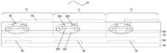
图1为本发明实施例提供的一种柔性显示基板的结构示意图一;FIG. 1 is a structural schematic diagram 1 of a flexible display substrate provided by an embodiment of the present invention;
图2为本发明实施例提供的一种柔性显示基板的结构示意图二;FIG. 2 is a schematic structural diagram II of a flexible display substrate provided by an embodiment of the present invention;
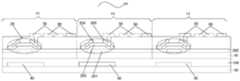
图3为本发明实施例提供的一种柔性显示基板的结构示意图三;FIG. 3 is a schematic structural diagram III of a flexible display substrate provided by an embodiment of the present invention;
图4为本发明实施例提供的一种柔性显示基板的结构示意图四;Fig. 4 is a structural schematic diagram 4 of a flexible display substrate provided by an embodiment of the present invention;
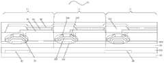
图5为本发明实施例提供的一种柔性显示基板的结构示意图五;Fig. 5 is a schematic structural diagram five of a flexible display substrate provided by an embodiment of the present invention;
图6为本发明实施例提供的一种柔性显示基板的结构示意图六;FIG. 6 is a schematic structural diagram VI of a flexible display substrate provided by an embodiment of the present invention;
图7为本发明实施例提供的一种柔性显示基板的结构示意图七;FIG. 7 is a schematic structural diagram VII of a flexible display substrate provided by an embodiment of the present invention;
图8为本发明实施例提供的一种柔性显示基板的结构示意图八;FIG. 8 is a schematic structural diagram eighth of a flexible display substrate provided by an embodiment of the present invention;
图9为本发明实施例提供的一种柔性显示器的结构示意图一;FIG. 9 is a first structural schematic diagram of a flexible display provided by an embodiment of the present invention;
图10为本发明实施例提供的一种柔性显示器的结构示意图二。FIG. 10 is a second structural schematic diagram of a flexible display provided by an embodiment of the present invention.
附图标记:Reference signs:
01-柔性显示基板;02-柔性封装基板;03-彩膜基板;04-液晶层;05-粘结胶;10-第一柔性衬底基板;11-显示元件;20-薄膜晶体管;30-第二柔性衬底基板;40-突起结构;50-像素电极;60-公共电极;70-阳极;80-阴极;90-有机材料功能层;100-OCA光学胶;110-像素隔离层;201-栅极;202-栅绝缘层;203-有源层;204-源极;205-漏极;300-第三柔性衬底基板;310-红色光阻;320-绿色光阻;330-蓝色光阻。01-flexible display substrate; 02-flexible packaging substrate; 03-color film substrate; 04-liquid crystal layer; 05-bonding glue; 10-first flexible substrate substrate; 11-display element; The second flexible substrate substrate; 40-protrusion structure; 50-pixel electrode; 60-common electrode; 70-anode; 80-cathode; 90-organic material functional layer; 100-OCA optical glue; -gate; 202-gate insulating layer; 203-active layer; 204-source; 205-drain; 300-third flexible substrate; 310-red photoresist; 320-green photoresist; 330-blue color photoresist.
具体实施方式Detailed ways
下面将结合本发明实施例中的附图,对本发明实施例中的技术方案进行清楚、完整地描述,显然,所描述的实施例仅仅是本发明一部分实施例,而不是全部的实施例。基于本发明中的实施例,本领域普通技术人员在没有做出创造性劳动前提下所获得的所有其他实施例,都属于本发明保护的范围。The following will clearly and completely describe the technical solutions in the embodiments of the present invention with reference to the accompanying drawings in the embodiments of the present invention. Obviously, the described embodiments are only some, not all, embodiments of the present invention. Based on the embodiments of the present invention, all other embodiments obtained by persons of ordinary skill in the art without making creative efforts belong to the protection scope of the present invention.
本发明实施例提供了一种柔性显示基板01,如图1-图8所示,所述柔性显示基板01包括第一柔性衬底基板10、以及设置在所述第一柔性衬底基板10上的多个显示元件11,所述显示元件11包括薄膜晶体管20;进一步所述柔性显示基板01还包括设置在所述第一柔性衬底基板10远离所述薄膜晶体管20一侧的第二柔性衬底基板30,以及设置在所述第一柔性衬底基板10和所述第二柔性衬底基板30之间的多个突起结构40。An embodiment of the present invention provides a
其中,任一个突起结构40在所述第二柔性衬底基板30上的投影与一个显示元件11中的所述薄膜晶体管20在所述第二柔性衬底基板30上的投影重叠。Wherein, the projection of any
所述薄膜晶体管20包括栅极201、栅绝缘层202、有源层203、源极204和漏极205等;在此情况下,所述柔性显示基板01还包括与所述栅极201电连接的栅线、栅线引线,与所述源极204电连接的数据线、数据线引线。The
此外,当所述柔性显示基板为液晶显示器(Liquid CrystalDisplay,简称LCD)的阵列基板时,如图1和图2所示,所述显示元件11还包括与所述漏极205相连接的像素电极50。当然所述显示元件11还可以包括公共电极60;在此情况下,对于共平面切换型(In-Plane Switch,简称IPS)阵列基板而言,如图3和图4所示,所述像素电极50和所述公共电极60同层间隔设置,且均为条状电极;对于高级超维场转换型(Advanced-super Dimensional Switching,简称ADS)阵列基板而言,如图5和图6所示,所述像素电极50和所述公共电极60不同层设置,其中在上的电极为条状电极,在下的电极为板状电极。In addition, when the flexible display substrate is an array substrate of a Liquid Crystal Display (LCD for short), as shown in FIG. 1 and FIG. 2 , the
当所述柔性显示基板为有机电致发光二极管(OrganicLight-Emitting Diode,简称OLED)的阵列基板时,如图7和图8所示,所述显示元件11还包括与所述漏极205相连接的阳极70、阴极80、以及位于所述阳极70和所述阴极80之间的有机材料功能层90。When the flexible display substrate is an array substrate of an organic light-emitting diode (OrganicLight-Emitting Diode, referred to as OLED), as shown in FIG. 7 and FIG. 8, the
在此情况下,根据所述阳极70和所述阴极80的材料的不同,可以分为单面发光型柔性显示基板和双面发光型柔性显示基板;即:当所述阳极70和所述阴极80中其中一个电极的材料为不透明材料时,所述柔性显示基板为单面发光型;当所述阳极70和所述阴极80的材料均为透明材料时,所述柔性显示基板为双面发光型。In this case, according to the different materials of the
对于单面发光型柔性显示基板,根据所述阳极70和所述阴极80的材料的不同,又可以分为上发光型和下发光型。具体的,当所述阳极70靠近所述第一柔性衬底基板10设置,所述阴极80远离所述第一柔性衬底基板10设置,且所述阳极70的材料为透明导电材料,所述阴极80的材料为不透明导电材料时,由于光从阳极70、再经第一柔性衬底基板10一侧出射,因此,可以称为下发光型;当所述阳极70的材料为不透明导电材料,所述阴极80的材料为透明导电材料时,由于光从阴极80、再经与第一柔性衬底基板10相对设置的封装层出射,因此,可以称为上发光型。当然,也可以将上述两种阳极70和阴极80的相对位置进行替换,在此再赘述。For the single-side emission type flexible display substrate, according to the different materials of the
这里,所述封装层可以是柔性封装基板,也可以是一层薄膜,在此不作限定。Here, the encapsulation layer may be a flexible encapsulation substrate, or a thin film, which is not limited here.
对于双面发光型柔性显示基板,当所述阳极70靠近所述第一柔性衬底基板10设置,所述阴极80远离所述第一柔性衬底基板10设置,或当所述阳极70远离所述第一柔性衬底基板10设置,所述阴极80靠近所述第一柔性衬底基板10设置,且所述阳极70和所述阴极80的材料均为透明导电材料例如ITO(Indium Tin Oxides,氧化铟锡)时,由于光一方面从阳极70、再经第一柔性衬底基板10一侧出射,另一方面从阴极80、再经与所述第一柔性衬底基板10相对设置的封装层出射,因此可以称为双面发光型。For a double-sided light-emitting flexible display substrate, when the
基于上述描述,所述显示元件11还可以包括一些必要的图案层例如保护层、钝化层、层间绝缘层、用于隔离像素单元的像素隔离层110等或为改善显示效果或某些缺陷增加的一些图案层。Based on the above description, the
需要说明的是,第一,在本发明实施例中,所述显示元件可以理解为,对应所述柔性显示基板01的一个最小的显示单元来说,设置在第一柔性衬底基板10上的必不可少的、且由各层图案组成的结构,且所述柔性显示基板01包括若干个所述显示元件。It should be noted that, first, in the embodiment of the present invention, the display element can be understood as, corresponding to a smallest display unit of the
第二,所述突起结构40可以通过构图工艺、喷墨打印工艺、丝网印刷等形成。Second, the
在此基础上,所述突起结构40可以设置在所述第一柔性衬底基板10远离所述薄膜晶体管20的一侧,也可以设置在所述第二柔性衬底基板30靠近所述第一柔性衬底基板10的一侧。On this basis, the protruding
第三,不对所述突起结构40的形状以及个数进行限定,以能在所述柔性显示基板01弯曲时,保护所述薄膜晶体管20不被破坏为准。这里,不管所述突起结构40的个数为多少个,对于任一个所述突起结构40来说,其必然与一个所述显示元件11中的薄膜晶体管20位置对应。Thirdly, the shape and number of the protruding
第四,上述的位置对应即为,任一个突起结构40在所述第二柔性衬底基板30上的投影与一个显示元件11中的所述薄膜晶体管20在所述第二柔性衬底基板30上的投影重叠;这里不对重叠多少进行限定,其可以是部分重叠,也可以是全部重叠,或者是面积相对较大的完全覆盖面积相对较小的,具体以能在所述柔性显示基板01弯曲时,保护所述薄膜晶体管20不被破坏,且所述突起结构40不会影响该柔性显示基板01的显示效果为准。Fourth, the above-mentioned position correspondence is that the projection of any
第五,所述薄膜晶体管20可以是顶栅型,也可以是底栅型,在此不作限定。其中,顶栅、底栅是相对所述栅极201和栅绝缘层202的位置而定的,即:相对所述第一柔性衬底基板10,当栅极201靠近所述第一柔性衬底基板10,栅绝缘层202远离所述第一柔性衬底基板10时,为底栅型薄膜晶体管;当栅极201远离所述第一柔性衬底基板10,栅绝缘层202靠近所述第一柔性衬底基板10时,为顶栅型薄膜晶体管。Fifth, the
本发明实施例提供了一种柔性显示基板01,包括第一柔性衬底基板10、以及设置在所述第一柔性衬底基板10上的多个显示元件11,所述显示元件11包括薄膜晶体管20;进一步所述柔性显示基板01还包括设置在所述第一柔性衬底基板10远离所述薄膜晶体管20一侧的第二柔性衬底基板30,以及设置在所述第一柔性衬底基板10和所述第二柔性衬底基板30之间的多个突起结构40;其中,任一个突起结构40在所述第二柔性衬底基板30上的投影与一个显示元件11中的所述薄膜晶体管20在所述第二柔性衬底基板30上的投影重叠。这样,当所述柔性显示基板01发生弯曲时,所述突起结构40便可以承载弯曲过程中产生的应力,从而防止所述柔性显示基板01在弯曲过程中产生应力破坏所述薄膜晶体管20。The embodiment of the present invention provides a
可选的,相对所述多个显示元件11,任意相邻两个所述突起结构40间隔设置。即:所述显示元件11的个数大于所述突起结构40的个数。Optionally, relative to the plurality of
这里,参考图1、3、5、7所示,相对所述多个显示元件11,所述突起结构40可以间隔设置,例如:沿栅线方向,所述突起结构40设置在第奇数个显示元件11的薄膜晶体管20的下方,或者所述突起结构40间隔至少2个显示元件11的所述薄膜晶体管20设置,具体根据实际情况进行设定,在此不做限定。Here, as shown in FIGS. 1, 3, 5, and 7, relative to the plurality of
进一步优选的,如图2、4、6、8所示,所述突起结构40与所述显示元件11一一对应,即:在任一个显示元件11的薄膜晶体管20的下方均设置有一个突起结构40。Further preferably, as shown in FIGS. 2 , 4 , 6 , and 8 , the
优选的,任一个所述突起结构40在所述第二柔性衬底基板30上的投影面积大于对应的所述显示元件11中的所述薄膜晶体管20在所述第二柔性衬底基板30上的投影面积。Preferably, the projected area of any one of the protruding
优选的,参考图1-8所示,所述突起结构40设置在所述第二柔性衬底基板30上,所述第一柔性衬底基板10和设置有所述突起结构40的所述第二柔性衬底基板30通过OCA光学胶100相粘结。即:将设置有所述突起结构40的第二柔性衬底基板30通过OCA光学胶100和设置有显示元件11的第一柔性衬底基板10相粘结。Preferably, as shown in FIGS. 1-8 , the protruding
基于上述的描述,可选的,所述突起结构40的形状可以为长方体、或正方体、或圆柱体、或多边体。Based on the above description, optionally, the shape of the protruding
可选的,所述突起结构40的材料可以是金属材料,例如为铝(Al)、钼(Mo)等,也可以是树脂材料,例如为聚酰亚胺,也可以是无机材料,例如为氮化硅(SiNx)、氧化硅(SiOx)等。例如可以通过构图工艺制备成型,即通过在所述第二柔性衬底基板30上沉积例如金属薄膜,并在金属薄膜上形成光刻胶,然后通过普通掩模板进行曝光、刻蚀、剥离等工艺形成所述突起结构40。Optionally, the material of the
这里考虑到构图工艺的限制,以及所述柔性显示基板01整体的厚度,所述突起结构40的厚度优选为0.2-2μm。Considering the limitations of the patterning process and the overall thickness of the
需要说明的是,形成所述突起结构40并不限于通过构图工艺形成,也可以通过其他方式实现,在此不再赘述。It should be noted that the formation of the protruding
本发明实施例还提供了一种柔性显示器,所述柔性显示器包括上述的所述柔性显示基板01。An embodiment of the present invention also provides a flexible display, which includes the above-mentioned
所述柔性显示器可以为:电子纸、液晶电视、液晶显示器、OLED电视、OLED显示器、数码相框、手机、平板电脑等具有任何显示功能的产品或部件。The flexible display can be: electronic paper, LCD TV, liquid crystal display, OLED TV, OLED display, digital photo frame, mobile phone, tablet computer and other products or components with any display function.
可选的,如图9所示,在所述柔性显示基板01为液晶显示器的阵列基板的情况下,即:在所述柔性显示基板01包括与所述薄膜晶体管20的漏极205电连接的像素电极50的情况下,所述柔性显示器还包括彩膜基板03,以及液晶层04。Optionally, as shown in FIG. 9, in the case where the
其中,所述彩膜基板03包括第三柔性衬底基板300,设置在所述第三柔性衬底基板300上的色层,所述色层包括红色光阻310、绿色光阻320和蓝色光阻330;当然也可以包括白色光阻,在此不做限定。Wherein, the color filter substrate 03 includes a third flexible substrate 300, and a colored layer disposed on the third flexible substrate 300, the colored layer includes a red photoresist 310, a green photoresist 320 and a blue photoresist. Resist 330; of course, it may also include white photoresist, which is not limited here.
在所述柔性显示基板01不包括公共电极60的情况下,所述彩膜基板02还包括所述公共电极60。In the case that the
可选的,如图10所示,在所述柔性显示基板01为OLED的阵列基板的情况下,即:在所述柔性显示基板01包括与所述薄膜晶体管20的漏极205电连接的阳极70、以及阴极80和有机材料功能层90的情况下,所述柔性显示器还包括柔性封装基板02;其中,所述柔性封装基板02与所述柔性显示基板01通过粘结胶05粘结。Optionally, as shown in FIG. 10 , in the case where the
其中,由于上述的所述有机材料功能层90的有机材料和作为电极的金属材料对氧气和水气相当敏感,渗透进入显示器内部的氧气和水气会影响显示面板的寿命,因此,所述OLED都会包括与所述第一柔性衬底基板10相对设置的柔性封装基板02来隔绝氧气和水气。当然也可以采用薄膜进行封装,在此不作限定。Wherein, since the above-mentioned organic material of the organic material
下面通过两个具体的实施例来详细描述上述的柔性显示器。The above flexible display will be described in detail below through two specific embodiments.
实施例一,参考图9所示,提供一种柔性液晶显示器,该柔性液晶显示器包括柔性显示基板01、彩膜基板03、以及设置在两基板之间的液晶层04。Embodiment 1, as shown in FIG. 9 , provides a flexible liquid crystal display, which includes a
所述柔性显示基板01包括由设置在第一柔性衬底基板10上的横纵交叉的栅线和数据线划分出的多个像素单元,每个像素单元包括一个显示元件11(图9中未标识),所述显示元件11包括薄膜晶体管20、像素电极50、以及公共电极60;其中,所述薄膜晶体管20包括栅极201、栅绝缘层202、有源层203、源极204和漏极205,所述像素电极50和所述漏极205电连接;所述像素电极50为板状电极,所述公共电极60位于所述像素电极50上方,且为条状电极。The
所述彩膜基板03包括第三柔性衬底基板300,设置在所述第三柔性衬底基板300上的色层,所述色层包括红色光阻310、绿色光阻320和蓝色光阻330。所述红色阻310、绿色光阻320和蓝色光阻330沿栅线方向循环排布,并与所述柔性显示基板01的像素单元一一对应。The color filter substrate 03 includes a third flexible substrate substrate 300, a colored layer disposed on the third flexible substrate substrate 300, and the colored layer includes a red photoresist 310, a green photoresist 320 and a blue photoresist 330 . The red photoresist 310 , the green photoresist 320 and the blue photoresist 330 are circularly arranged along the grid line direction and correspond to the pixel units of the
在此基础上,所述柔性显示基板01还包括第二柔性衬底基板30以及设置在所述第二柔性衬底基板30上的多个突起结构40;所述第一柔性衬底基板10远离薄膜晶体管20的一侧和设置有所述突起结构40的所述第二柔性衬底基板30的一侧通过OCA光学胶100相粘结;其中,在任一个显示元件11的薄膜晶体管20的下方均设置有一个突起结构40,且所述突起结构40在所述第二柔性衬底基板30上的投影面积大于所述薄膜晶体管20在所述第二柔性衬底基板30上的投影面积。On this basis, the
此外,所述突起结构40的材料为聚酰亚胺、形状为长方体,厚度为1μm。In addition, the material of the
本发明实施例提供的一种柔性液晶显示器,当所述柔性液晶显示器发生弯曲时,由于所述突起结构40的存在,其可以承载弯曲过程中产生的应力,从而防止所述柔性液晶显示器在弯曲过程中产生应力破坏所述薄膜晶体管20。In the flexible liquid crystal display provided by the embodiment of the present invention, when the flexible liquid crystal display is bent, due to the existence of the
实施例二,参考图10所示,提供一种柔性有机电致发光二极管显示器,该柔性有机电致发光二极管显示器包括柔性显示基板01和柔性封装基板02,所述柔性封装基板02与所述柔性显示基板01通过粘结胶05粘结。Embodiment 2, as shown in FIG. 10 , provides a flexible organic electroluminescent diode display, the flexible organic electroluminescent diode display includes a
所述柔性显示基板01包括多个像素单元,每个像素单元包括一个显示元件11(图9中未标识),所述显示元件11包括:薄膜晶体管20、阳极70、阴极80、以及位于所述阳极70和所述阴极80之间的有机材料功能层90。相邻的两个像素单元通过设置在所述薄膜晶体管20上方的像素隔离层110来隔离。The
其中,所述薄膜晶体管20包括栅极201、栅绝缘层202、有源层203、源极204和漏极205,所述阳极70和所述漏极205电连接;所述阴极80位于所述阳极70上方,且所述阳极70材料为透明材料,阴极80材料为不透明材料;所述有机材料功能层90至少包括电子传输层、发光层和空穴传输层;为了能够提高所述电子和所述空穴注入发光层的效率,所述有机材料功能层90还可以包括设置在所述阴极80与所述电子传输层之间的电子注入层,以及在所述阳极70与所述空穴传输层之间的空穴注入层。Wherein, the
在此基础上,所述柔性显示基板01还包括第二柔性衬底基板30以及设置在所述第二柔性衬底基板30上的多个突起结构40;所述第一柔性衬底基板10远离薄膜晶体管20的一侧和设置有所述突起结构40的所述第二柔性衬底基板30的一侧通过OCA光学胶100相粘结;其中,在任一个显示元件11的薄膜晶体管20的下方均设置有一个突起结构40,且所述突起结构40在所述第二柔性衬底基板30上的投影面积大于所述薄膜晶体管20在所述第二柔性衬底基板30上的投影面积。On this basis, the
此外,所述突起结构40的材料为聚酰亚胺、形状为长方体,厚度为1μm。In addition, the material of the
本发明实施例提供的一种柔性有机电致发光二极管显示器,当所述柔性有机电致发光二极管显示器发生弯曲时,由于所述突起结构40的存在,其可以承载弯曲过程中产生的应力,从而防止所述柔性有机电致发光二极管显示器在弯曲过程中产生应力破坏所述薄膜晶体管20。In the flexible organic electroluminescent diode display provided by the embodiment of the present invention, when the flexible organic electroluminescent diode display is bent, due to the existence of the
基于上述描述,本领域技术人员应该明白,本发明实施例中所有附图是所述柔性显示基板和柔性显示器的简略示意图,只为清楚描述本方案中与本发明点相关的结构,对于其他的与本发明点无关的结构是现有结构,在附图中并未体现或只体现部分。Based on the above description, those skilled in the art should understand that all the drawings in the embodiments of the present invention are simplified schematic diagrams of the flexible display substrate and the flexible display, and are only for clearly describing the structure related to the present invention in this solution. For other The structure irrelevant to the point of the present invention is an existing structure, which is not shown or only partly shown in the drawings.
以上所述,仅为本发明的具体实施方式,但本发明的保护范围并不局限于此,任何熟悉本技术领域的技术人员在本发明揭露的技术范围内,可轻易想到变化或替换,都应涵盖在本发明的保护范围之内。因此,本发明的保护范围应以所述权利要求的保护范围为准。The above is only a specific embodiment of the present invention, but the scope of protection of the present invention is not limited thereto. Anyone skilled in the art can easily think of changes or substitutions within the technical scope disclosed in the present invention. Should be covered within the protection scope of the present invention. Therefore, the protection scope of the present invention should be determined by the protection scope of the claims.
Claims (12)
Translated fromChinesePriority Applications (3)
| Application Number | Priority Date | Filing Date | Title |
|---|---|---|---|
| CN201310658988.6ACN103681694A (en) | 2013-12-06 | 2013-12-06 | Flexible display substrate and flexible display device |
| US14/418,235US10644032B2 (en) | 2013-12-06 | 2014-05-29 | Flexible display substrate and flexible display |
| PCT/CN2014/078805WO2015081674A1 (en) | 2013-12-06 | 2014-05-29 | Flexible display substrate and flexible display |
Applications Claiming Priority (1)
| Application Number | Priority Date | Filing Date | Title |
|---|---|---|---|
| CN201310658988.6ACN103681694A (en) | 2013-12-06 | 2013-12-06 | Flexible display substrate and flexible display device |
Publications (1)
| Publication Number | Publication Date |
|---|---|
| CN103681694Atrue CN103681694A (en) | 2014-03-26 |
Family
ID=50318713
Family Applications (1)
| Application Number | Title | Priority Date | Filing Date |
|---|---|---|---|
| CN201310658988.6APendingCN103681694A (en) | 2013-12-06 | 2013-12-06 | Flexible display substrate and flexible display device |
Country Status (3)
| Country | Link |
|---|---|
| US (1) | US10644032B2 (en) |
| CN (1) | CN103681694A (en) |
| WO (1) | WO2015081674A1 (en) |
Cited By (7)
| Publication number | Priority date | Publication date | Assignee | Title |
|---|---|---|---|---|
| WO2015081674A1 (en)* | 2013-12-06 | 2015-06-11 | 京东方科技集团股份有限公司 | Flexible display substrate and flexible display |
| CN106558279A (en)* | 2017-01-13 | 2017-04-05 | 京东方科技集团股份有限公司 | Flexible display apparatus and preparation method thereof |
| CN107768298A (en)* | 2017-10-18 | 2018-03-06 | 武汉华星光电技术有限公司 | A kind of preparation method of the composite base plate prepared for flexible TFT and flexible panel |
| CN108257982A (en)* | 2018-01-23 | 2018-07-06 | 京东方科技集团股份有限公司 | Flexible substrate substrate and its manufacturing method, flexible panel and electronic equipment |
| WO2020077718A1 (en)* | 2018-10-18 | 2020-04-23 | 武汉华星光电半导体显示技术有限公司 | Array substrate and manufacturing method thereof, and display module |
| CN113053915A (en)* | 2021-03-08 | 2021-06-29 | 武汉华星光电半导体显示技术有限公司 | Display panel and preparation method thereof |
| CN119179402A (en)* | 2024-11-25 | 2024-12-24 | 惠科股份有限公司 | Touch component, touch display device and electronic equipment |
Families Citing this family (4)
| Publication number | Priority date | Publication date | Assignee | Title |
|---|---|---|---|---|
| US10388904B2 (en)* | 2014-11-07 | 2019-08-20 | Sharp Kabushiki Kaisha | Organic el display device and method for producing organic el display device |
| CN105425493B (en)* | 2016-01-11 | 2018-10-23 | 京东方科技集团股份有限公司 | A kind of array substrate and preparation method thereof, display panel |
| CN107611090B (en)* | 2017-09-15 | 2021-07-23 | 深圳市华星光电半导体显示技术有限公司 | OLED display panel and preparation method thereof |
| CN109037239B (en)* | 2018-07-26 | 2020-11-17 | 上海天马微电子有限公司 | Array substrate, preparation method thereof and display panel |
Citations (5)
| Publication number | Priority date | Publication date | Assignee | Title |
|---|---|---|---|---|
| CN1460299A (en)* | 2001-04-03 | 2003-12-03 | 皇家菲利浦电子有限公司 | Matrix array devices with flexible substrates |
| CN1753586A (en)* | 2005-08-26 | 2006-03-29 | 友达光电股份有限公司 | Organic electroluminescence display and manufacturing method thereof |
| US20070235736A1 (en)* | 2002-05-17 | 2007-10-11 | Kabushiki Kaisha Toshiba | Active matrix type display device and method of manufacturing the same |
| US20100141872A1 (en)* | 2008-12-04 | 2010-06-10 | Seung-Han Paek | Flexible liquid crystal display device |
| CN103426904A (en)* | 2013-08-02 | 2013-12-04 | 京东方科技集团股份有限公司 | Flexible organic light-emitting diode display and method for manufacturing same |
Family Cites Families (9)
| Publication number | Priority date | Publication date | Assignee | Title |
|---|---|---|---|---|
| JPH08186336A (en) | 1994-12-28 | 1996-07-16 | Mitsubishi Electric Corp | Circuit board, drive circuit module, liquid crystal display device using the same, and manufacturing method thereof |
| US7439096B2 (en) | 2001-02-21 | 2008-10-21 | Lucent Technologies Inc. | Semiconductor device encapsulation |
| KR100615235B1 (en) | 2004-08-05 | 2006-08-25 | 삼성에스디아이 주식회사 | Organic thin film transistor groups and flat panel display device having same |
| TWI415044B (en)* | 2008-12-15 | 2013-11-11 | Ind Tech Res Inst | Substrate board, fabrication method thereof and a display therewith |
| JP2011248072A (en)* | 2010-05-26 | 2011-12-08 | Hitachi Displays Ltd | Method of manufacturing image display device |
| CN102969320B (en) | 2012-12-10 | 2015-10-21 | 京东方科技集团股份有限公司 | Flexible display substrates and preparation method thereof, flexible display apparatus |
| CN103489880B (en)* | 2013-10-12 | 2015-03-25 | 京东方科技集团股份有限公司 | Display substrate and flexible display device containing same |
| CN103681694A (en) | 2013-12-06 | 2014-03-26 | 京东方科技集团股份有限公司 | Flexible display substrate and flexible display device |
| CN103855171B (en)* | 2014-02-28 | 2017-01-18 | 京东方科技集团股份有限公司 | Flexible display substrate mother board and manufacturing method of flexible display substrate |
- 2013
- 2013-12-06CNCN201310658988.6Apatent/CN103681694A/enactivePending
- 2014
- 2014-05-29WOPCT/CN2014/078805patent/WO2015081674A1/enactiveApplication Filing
- 2014-05-29USUS14/418,235patent/US10644032B2/enactiveActive
Patent Citations (5)
| Publication number | Priority date | Publication date | Assignee | Title |
|---|---|---|---|---|
| CN1460299A (en)* | 2001-04-03 | 2003-12-03 | 皇家菲利浦电子有限公司 | Matrix array devices with flexible substrates |
| US20070235736A1 (en)* | 2002-05-17 | 2007-10-11 | Kabushiki Kaisha Toshiba | Active matrix type display device and method of manufacturing the same |
| CN1753586A (en)* | 2005-08-26 | 2006-03-29 | 友达光电股份有限公司 | Organic electroluminescence display and manufacturing method thereof |
| US20100141872A1 (en)* | 2008-12-04 | 2010-06-10 | Seung-Han Paek | Flexible liquid crystal display device |
| CN103426904A (en)* | 2013-08-02 | 2013-12-04 | 京东方科技集团股份有限公司 | Flexible organic light-emitting diode display and method for manufacturing same |
Cited By (11)
| Publication number | Priority date | Publication date | Assignee | Title |
|---|---|---|---|---|
| WO2015081674A1 (en)* | 2013-12-06 | 2015-06-11 | 京东方科技集团股份有限公司 | Flexible display substrate and flexible display |
| US10644032B2 (en) | 2013-12-06 | 2020-05-05 | Boe Technology Group Co., Ltd. | Flexible display substrate and flexible display |
| CN106558279A (en)* | 2017-01-13 | 2017-04-05 | 京东方科技集团股份有限公司 | Flexible display apparatus and preparation method thereof |
| US10651405B2 (en) | 2017-01-13 | 2020-05-12 | Boe Technology Group Co., Ltd. | Flexible display device and manufacturing method thereof |
| CN107768298A (en)* | 2017-10-18 | 2018-03-06 | 武汉华星光电技术有限公司 | A kind of preparation method of the composite base plate prepared for flexible TFT and flexible panel |
| CN108257982A (en)* | 2018-01-23 | 2018-07-06 | 京东方科技集团股份有限公司 | Flexible substrate substrate and its manufacturing method, flexible panel and electronic equipment |
| CN108257982B (en)* | 2018-01-23 | 2021-01-29 | 京东方科技集团股份有限公司 | Flexible substrate, method for manufacturing same, flexible panel, and electronic device |
| WO2020077718A1 (en)* | 2018-10-18 | 2020-04-23 | 武汉华星光电半导体显示技术有限公司 | Array substrate and manufacturing method thereof, and display module |
| CN113053915A (en)* | 2021-03-08 | 2021-06-29 | 武汉华星光电半导体显示技术有限公司 | Display panel and preparation method thereof |
| US11991917B2 (en) | 2021-03-08 | 2024-05-21 | Wuhan China Star Optoelectronics Semiconductor Display Technology Co., Ltd. | Display panel and manufacturing method thereof |
| CN119179402A (en)* | 2024-11-25 | 2024-12-24 | 惠科股份有限公司 | Touch component, touch display device and electronic equipment |
Also Published As
| Publication number | Publication date |
|---|---|
| US20160020226A1 (en) | 2016-01-21 |
| WO2015081674A1 (en) | 2015-06-11 |
| US10644032B2 (en) | 2020-05-05 |
Similar Documents
| Publication | Publication Date | Title |
|---|---|---|
| CN103681694A (en) | Flexible display substrate and flexible display device | |
| CN108766994B (en) | Organic light-emitting display panel and organic light-emitting display device | |
| US10090326B2 (en) | Flexible display substrate and a manufacturing method thereof, as well as a flexible display device | |
| US9831297B2 (en) | AMOLED array substrate, method for manufacturing the same and display device | |
| TWI578593B (en) | Organic light emitting diode device and method of manufacturing same | |
| US12058880B2 (en) | Display substrate, manufacturing method thereof and display panel | |
| US11552152B2 (en) | Display device including a power supply voltage wiring having openings | |
| US9515129B2 (en) | Organic light emitting display apparatus and manufacturing method thereof | |
| CN103779390B (en) | A kind of flexible display substrates and preparation method thereof | |
| CN107123621A (en) | A kind of OLED touch-control display panels and preparation method thereof, touch control display apparatus | |
| KR102255063B1 (en) | Organic Light Emitting Diode Display Device | |
| JP2017187580A (en) | Display device | |
| CN108376688A (en) | A kind of photosensory assembly and preparation method thereof, array substrate, display device | |
| CN103700675A (en) | AMOLED array substrate and display device | |
| CN109004005A (en) | Display panel and preparation method thereof, display device | |
| CN104659072A (en) | Array substrate and manufacturing method thereof | |
| CN103715205A (en) | AMOLED array substrate and display device | |
| CN110098227B (en) | OLED display panel and manufacturing method thereof | |
| CN106876416A (en) | Static discharge unit, array base palte and display panel | |
| CN104576694A (en) | Oled display device and manufacturing method thereof | |
| CN109119451A (en) | Display base plate and its manufacturing method, display device | |
| CN207164732U (en) | A kind of touch-control display panel and touch control display apparatus | |
| CN104571716B (en) | Upper substrate and preparation method, touch-control display panel and preparation method | |
| WO2021121095A1 (en) | Array substrate, display panel, and display device | |
| JP2017187581A (en) | Display device |
Legal Events
| Date | Code | Title | Description |
|---|---|---|---|
| PB01 | Publication | ||
| PB01 | Publication | ||
| C10 | Entry into substantive examination | ||
| SE01 | Entry into force of request for substantive examination | ||
| RJ01 | Rejection of invention patent application after publication | ||
| RJ01 | Rejection of invention patent application after publication | Application publication date:20140326 |