CN103680633A - One-time programmable memory cell - Google Patents
One-time programmable memory cellDownload PDFInfo
- Publication number
- CN103680633A CN103680633ACN201310404318.1ACN201310404318ACN103680633ACN 103680633 ACN103680633 ACN 103680633ACN 201310404318 ACN201310404318 ACN 201310404318ACN 103680633 ACN103680633 ACN 103680633A
- Authority
- CN
- China
- Prior art keywords
- oxide
- thick
- transistor
- access transistor
- memory cell
- Prior art date
- Legal status (The legal status is an assumption and is not a legal conclusion. Google has not performed a legal analysis and makes no representation as to the accuracy of the status listed.)
- Granted
Links
- 239000000758substrateSubstances0.000claimsdescription50
- 238000009792diffusion processMethods0.000claimsdescription14
- 238000000034methodMethods0.000claimsdescription9
- 230000008569processEffects0.000claimsdescription5
- 238000002347injectionMethods0.000claims6
- 239000007924injectionSubstances0.000claims6
- 125000006850spacer groupChemical group0.000abstractdescription78
- 229910021420polycrystalline siliconInorganic materials0.000description13
- 229920005591polysiliconPolymers0.000description13
- 238000002513implantationMethods0.000description10
- 239000000463materialSubstances0.000description6
- 229910052710siliconInorganic materials0.000description4
- 239000010703siliconSubstances0.000description4
- 239000002019doping agentSubstances0.000description3
- 239000007943implantSubstances0.000description3
- 230000004048modificationEffects0.000description3
- 238000012986modificationMethods0.000description3
- 230000008901benefitEffects0.000description2
- 230000006870functionEffects0.000description2
- 239000000203mixtureSubstances0.000description2
- 230000003287optical effectEffects0.000description2
- 230000006978adaptationEffects0.000description1
- 230000015556catabolic processEffects0.000description1
- 230000008878couplingEffects0.000description1
- 238000010168coupling processMethods0.000description1
- 238000005859coupling reactionMethods0.000description1
- 238000013500data storageMethods0.000description1
- 230000000694effectsEffects0.000description1
- 230000007246mechanismEffects0.000description1
- 230000000644propagated effectEffects0.000description1
- 230000008672reprogrammingEffects0.000description1
Images


Classifications
- H—ELECTRICITY
- H01—ELECTRIC ELEMENTS
- H01L—SEMICONDUCTOR DEVICES NOT COVERED BY CLASS H10
- H01L23/00—Details of semiconductor or other solid state devices
- H01L23/52—Arrangements for conducting electric current within the device in operation from one component to another, i.e. interconnections, e.g. wires, lead frames
- H01L23/522—Arrangements for conducting electric current within the device in operation from one component to another, i.e. interconnections, e.g. wires, lead frames including external interconnections consisting of a multilayer structure of conductive and insulating layers inseparably formed on the semiconductor body
- H01L23/525—Arrangements for conducting electric current within the device in operation from one component to another, i.e. interconnections, e.g. wires, lead frames including external interconnections consisting of a multilayer structure of conductive and insulating layers inseparably formed on the semiconductor body with adaptable interconnections
- H01L23/5252—Arrangements for conducting electric current within the device in operation from one component to another, i.e. interconnections, e.g. wires, lead frames including external interconnections consisting of a multilayer structure of conductive and insulating layers inseparably formed on the semiconductor body with adaptable interconnections comprising anti-fuses, i.e. connections having their state changed from non-conductive to conductive
- H—ELECTRICITY
- H10—SEMICONDUCTOR DEVICES; ELECTRIC SOLID-STATE DEVICES NOT OTHERWISE PROVIDED FOR
- H10B—ELECTRONIC MEMORY DEVICES
- H10B20/00—Read-only memory [ROM] devices
- H10B20/20—Programmable ROM [PROM] devices comprising field-effect components
- H10B20/25—One-time programmable ROM [OTPROM] devices, e.g. using electrically-fusible links
- H—ELECTRICITY
- H10—SEMICONDUCTOR DEVICES; ELECTRIC SOLID-STATE DEVICES NOT OTHERWISE PROVIDED FOR
- H10D—INORGANIC ELECTRIC SEMICONDUCTOR DEVICES
- H10D84/00—Integrated devices formed in or on semiconductor substrates that comprise only semiconducting layers, e.g. on Si wafers or on GaAs-on-Si wafers
- H10D84/80—Integrated devices formed in or on semiconductor substrates that comprise only semiconducting layers, e.g. on Si wafers or on GaAs-on-Si wafers characterised by the integration of at least one component covered by groups H10D12/00 or H10D30/00, e.g. integration of IGFETs
- H10D84/811—Combinations of field-effect devices and one or more diodes, capacitors or resistors
- H—ELECTRICITY
- H01—ELECTRIC ELEMENTS
- H01L—SEMICONDUCTOR DEVICES NOT COVERED BY CLASS H10
- H01L2924/00—Indexing scheme for arrangements or methods for connecting or disconnecting semiconductor or solid-state bodies as covered by H01L24/00
- H01L2924/0001—Technical content checked by a classifier
- H01L2924/0002—Not covered by any one of groups H01L24/00, H01L24/00 and H01L2224/00
Landscapes
- Physics & Mathematics (AREA)
- Condensed Matter Physics & Semiconductors (AREA)
- General Physics & Mathematics (AREA)
- Engineering & Computer Science (AREA)
- Computer Hardware Design (AREA)
- Microelectronics & Electronic Packaging (AREA)
- Power Engineering (AREA)
- Semiconductor Memories (AREA)
- Read Only Memory (AREA)
Abstract
Translated fromChinese
Description
Translated fromChinese技术领域technical field
本申请主要涉及存储设备,更具体地,涉及一次性可编程(OTP)存储单元。This application relates generally to memory devices, and more particularly to one-time programmable (OTP) memory cells.
背景技术Background technique
数据存储领域包括易失性存储器和非易失性存储器。当从易失性存储器电路上移除电源时,易失性存储器会丢失所存储的信息。非易失性存储器即使在移除电源之后,也会保留所存储的信息。某些非易失性存储器设计允许重新编程,而其他设计仅允许一次性编程。The field of data storage includes both volatile memory and nonvolatile memory. Volatile memory loses stored information when power is removed from the volatile memory circuitry. Nonvolatile memory retains stored information even after power is removed. Some nonvolatile memory designs allow reprogramming, while others only allow one-time programming.
一次性可编程(OTP)存储器表示一种非易失性存储器,该非易失性存储器通常通过打开熔丝以创建高阻抗连接或通过永久闭合抗熔丝以创建低阻抗连接来一次性编程。抗熔丝可以通过施加高电压以破坏抗熔丝并创建低阻抗连接而被编程。One-Time Programmable (OTP) memory means a type of non-volatile memory that is programmed once, usually by opening a fuse to create a high-impedance connection or by permanently closing an anti-fuse to create a low-impedance connection. An anti-fuse can be programmed by applying a high voltage to destroy the anti-fuse and create a low impedance connection.
利用抗熔丝的OTP存储单元继编程之后可以表现出不可预测且宽的IV(电流-电压)特性,因为抗熔丝断裂部位位置可能随设备的不同而不同。因此,需要一种表现出改进可预测性和改进IV特性的OTP存储单元。OTP memory cells utilizing anti-fuse can exhibit unpredictable and wide IV (current-voltage) characteristics after programming because the anti-fuse rupture location may vary from device to device. Accordingly, there is a need for an OTP memory cell that exhibits improved predictability and improved IV characteristics.
发明内容Contents of the invention
根据本发明的一个方面,提供了一种可编程存储单元,包括:基板,包括原生掺杂注入区;厚氧化物隔离件晶体管,设置在所述原生掺杂注入区内的所述基板上;可编程薄氧化物抗熔丝,设置在与所述厚氧化物隔离件晶体管的第一侧相邻的所述基板上并位于所述基板的所述原生掺杂注入区内;以及第一厚氧化物存取晶体管和第二厚氧化物存取晶体管,设置在所述基板上,所述第一厚氧化物存取晶体管设置在所述厚氧化物隔离件晶体管的第二侧与所述第二厚氧化物存取晶体管之间。According to one aspect of the present invention, a programmable memory unit is provided, comprising: a substrate including a native doping implantation region; a thick oxide spacer transistor disposed on the substrate in the native doping implantation region; a programmable thin oxide antifuse disposed on the substrate adjacent to the first side of the thick oxide spacer transistor and within the native dopant implant region of the substrate; and a first thick an oxide access transistor and a second thick oxide access transistor disposed on the substrate, the first thick oxide access transistor disposed on the second side of the thick oxide spacer transistor and the second side of the thick oxide spacer transistor between two thick oxide access transistors.
其中,所述第一厚氧化物晶体管和所述第二厚氧化物晶体管设置在所述原生掺杂注入区外的所述基板上。Wherein, the first thick oxide transistor and the second thick oxide transistor are disposed on the substrate outside the native doping implantation region.
其中,所述第一厚氧化物晶体管和所述第二厚氧化物晶体管设置在所述基板的已受过标准阈值电压注入处理的区域上。Wherein, the first thick oxide transistor and the second thick oxide transistor are disposed on a region of the substrate that has undergone a standard threshold voltage implantation process.
其中,所述基板的除所述原生掺杂注入区之外的区域已受过标准阈值电压注入处理。Wherein, the region of the substrate other than the native dopant implantation region has been subjected to standard threshold voltage implantation treatment.
其中,所述第一厚氧化物存取晶体管的漏极区用作所述厚氧化物隔离件晶体管的源极区。Wherein, the drain region of the first thick oxide access transistor is used as the source region of the thick oxide spacer transistor.
其中,所述第一厚氧化物存取晶体管的源极区用作所述第二厚氧化物存取晶体管的漏极区。Wherein, the source region of the first thick oxide access transistor is used as the drain region of the second thick oxide access transistor.
其中,所述原生掺杂注入区的边缘形成在所述第一厚氧化物存取晶体管的漏极区中。Wherein, the edge of the native doping implantation region is formed in the drain region of the first thick oxide access transistor.
其中,所述厚氧化物隔离件晶体管的栅极和所述抗熔丝并联耦接至第一输入端。Wherein, the gate of the thick oxide spacer transistor and the anti-fuse are coupled in parallel to the first input terminal.
其中,所述第一厚氧化物存取晶体管的栅极和所述第二厚氧化物存取晶体管的栅极分别连接至第二输入端和第三输入端。Wherein, the gate of the first thick oxide access transistor and the gate of the second thick oxide access transistor are respectively connected to the second input terminal and the third input terminal.
其中,所述可编程薄氧化物抗熔丝的氧化层具有第一厚度;以及所述厚氧化物隔离件晶体管、所述第一厚氧化物存取晶体管和所述第二厚氧化物存取晶体管中的每一个的氧化层具有大于所述第一厚度的第二厚度。Wherein, the oxide layer of the programmable thin oxide antifuse has a first thickness; and the thick oxide spacer transistor, the first thick oxide access transistor, and the second thick oxide access transistor The oxide layer of each of the transistors has a second thickness greater than the first thickness.
根据本发明的又一个方面,提供了一种可编程存储单元,包括:可编程薄氧化物抗熔丝,具有第一端和第二端;厚氧化物隔离件晶体管,连接至所述可编程薄氧化物抗熔丝的所述第一端和所述第二端;第一厚氧化物存取晶体管,经由第一扩散区连接至所述厚氧化物隔离件晶体管;以及第二厚氧化物存取晶体管,经由第二扩散区连接至所述第一厚氧化物存取晶体管,其中,所述可编程薄氧化物抗熔丝和所述厚氧化物隔离件晶体管具有与所述第一厚氧化物存取晶体管和所述第二厚氧化物存取晶体管不同的掺杂浓度。According to yet another aspect of the present invention, there is provided a programmable memory cell, comprising: a programmable thin oxide antifuse having a first terminal and a second terminal; a thick oxide spacer transistor connected to the programmable said first terminal and said second terminal of a thin oxide antifuse; a first thick oxide access transistor connected to said thick oxide spacer transistor via a first diffusion region; and a second thick oxide an access transistor connected to the first thick oxide access transistor via a second diffusion region, wherein the programmable thin oxide antifuse and the thick oxide spacer transistor have the same The oxide access transistor and the second thick oxide access transistor have different doping concentrations.
其中,所述可编程薄氧化物抗熔丝和所述厚氧化物隔离件晶体管被原生掺杂。Wherein the programmable thin oxide antifuse and the thick oxide spacer transistors are natively doped.
其中,所述第一厚氧化物存取晶体管和所述第二厚氧化物存取晶体管被掺杂从而具有标准阈值电压特性。Wherein, the first thick oxide access transistor and the second thick oxide access transistor are doped to have standard threshold voltage characteristics.
其中,所述第一扩散区用作所述厚氧化物隔离件晶体管的源极区和所述第一厚氧化物隔离件晶体管的漏极区。Wherein, the first diffusion region is used as a source region of the thick oxide spacer transistor and a drain region of the first thick oxide spacer transistor.
其中,所述第二扩散区用作所述第一厚氧化物存取晶体管的源极区和所述第二厚氧化物存取晶体管的漏极区。Wherein, the second diffusion region is used as a source region of the first thick oxide access transistor and a drain region of the second thick oxide access transistor.
其中,所述可编程存储单元进一步包括用作所述第二厚氧化物存取晶体管的源极区的第三扩散区。Wherein, the programmable memory cell further includes a third diffusion region serving as a source region of the second thick oxide access transistor.
其中:所述可编程薄氧化物抗熔丝的氧化层具有第一厚度;以及所述厚氧化物隔离件晶体管、所述第一厚氧化物存取晶体管和所述第二厚氧化物存取晶体管中的每一个的氧化层具有大于所述第一厚度的第二厚度。wherein: the oxide layer of the programmable thin oxide antifuse has a first thickness; and the thick oxide spacer transistor, the first thick oxide access transistor, and the second thick oxide access transistor The oxide layer of each of the transistors has a second thickness greater than the first thickness.
根据本发明的另一方面,提供了一种可编程存储单元,包括:可编程薄氧化物抗熔丝,连接至厚氧化物隔离件晶体管,所述可编程薄氧化物抗熔丝包括具有第一厚度的第一氧化层;第一厚氧化物存取晶体管,连接至所述厚氧化物隔离件晶体管;以及第二厚氧化物存取晶体管,连接至所述第一厚氧化物存取晶体管,其中,所述厚氧化物隔离件晶体管、所述第一厚氧化物存取晶体管和所述第二厚氧化物存取晶体管各自包括具有大于所述第一厚度的第二厚度的第二氧化层,其中,所述可编程薄氧化物抗熔丝和所述厚氧化物隔离件晶体管被原生掺杂,并且所述第一厚氧化物存取晶体管和所述第二厚氧化物存取晶体管被掺杂从而具有标准阈值电压特性。According to another aspect of the present invention, there is provided a programmable memory cell comprising: a programmable thin oxide antifuse connected to a thick oxide spacer transistor, said programmable thin oxide antifuse comprising a first a thickness of the first oxide layer; a first thick oxide access transistor connected to the thick oxide spacer transistor; and a second thick oxide access transistor connected to the first thick oxide access transistor , wherein the thick oxide spacer transistor, the first thick oxide access transistor, and the second thick oxide access transistor each include a second oxide having a second thickness greater than the first thickness layer, wherein the programmable thin oxide antifuse and the thick oxide spacer transistors are natively doped, and the first thick oxide access transistor and the second thick oxide access transistor Doped to have standard threshold voltage characteristics.
其中,所述可编程存储单元利用多个电压来编程,所述多个电压包括:编程电压,施加至所述可编程薄氧化物抗熔丝和所述厚氧化物隔离件晶体管;第一电源电压,施加至所述第一厚氧化物存取晶体管;第二电源电压,施加至所述第二厚氧化物存取晶体管,所述编程电压大于所述第一电源电压,并且所述第一电源电压大于所述第二电源电压;以及接地电压,施加至所述第二厚氧化物存取晶体管的源极区。Wherein, the programmable memory cell is programmed using a plurality of voltages, the plurality of voltages comprising: a programming voltage applied to the programmable thin oxide antifuse and the thick oxide spacer transistor; a first power supply voltage applied to the first thick oxide access transistor; a second supply voltage applied to the second thick oxide access transistor, the programming voltage is greater than the first supply voltage, and the first a power supply voltage greater than the second power supply voltage; and a ground voltage applied to a source region of the second thick oxide access transistor.
其中,所述可编程存储单元利用多个电压来读取,所述多个电压包括:读取电压,施加至所述可编程薄氧化物抗熔丝和所述厚氧化物隔离件晶体管;电源电压,施加至所述第一厚氧化物存取晶体管和所述第二厚氧化物存取晶体管,其中,所述读取电压小于所述电源电压;接地电压,施加至所述第二厚氧化物存取晶体管的源极区;以及其中,所述可编程薄氧化物抗熔丝处的电压电位被测量并与所施加的读取电压进行比较。Wherein, the programmable memory cell is read using a plurality of voltages, the plurality of voltages comprising: a read voltage applied to the programmable thin oxide antifuse and the thick oxide spacer transistor; a power supply a voltage applied to the first thick oxide access transistor and the second thick oxide access transistor, wherein the read voltage is less than the supply voltage; a ground voltage is applied to the second thick oxide the source region of the object access transistor; and wherein the voltage potential at the programmable thin oxide antifuse is measured and compared to the applied read voltage.
附图说明Description of drawings
并入本文并形成本说明书的一部分的附图示出了本发明的实施方式,并且与描述一起进一步用来阐述实施方式的原理并使相关技术的技术人员能够作出并使用所述实施方式。The accompanying drawings, which are incorporated in and form a part of this specification, illustrate embodiments of the invention and, together with the description, further serve to explain the principles of the embodiments and to enable those skilled in the relevant art to make and use the same.
图1示出了传统OTP存储单元电路。FIG. 1 shows a conventional OTP memory cell circuit.
图2示出了传统OTP存储单元截面。Figure 2 shows a cross section of a conventional OTP memory cell.
图3示出了根据本发明的示例性实施方式的示例性OTP存储单元电路。FIG. 3 illustrates an exemplary OTP memory cell circuit according to an exemplary embodiment of the present invention.
图4示出了根据本发明的示例性实施方式的示例性OTP存储单元截面。Figure 4 shows a cross section of an exemplary OTP memory cell according to an exemplary embodiment of the present invention.
图5示出了根据本发明的示例性实施方式的示例性OTP存储单元截面。FIG. 5 shows a cross section of an exemplary OTP memory cell according to an exemplary embodiment of the present invention.
图6示出了根据本发明的示例性实施方式的示例性OTP存储单元电路。FIG. 6 shows an exemplary OTP memory cell circuit according to an exemplary embodiment of the present invention.
图7示出了根据本发明的示例性实施方式的示例性OTP存储单元电路。FIG. 7 shows an exemplary OTP memory cell circuit according to an exemplary embodiment of the present invention.
将参照附图对本发明的实施方式进行描述。元件首次出现的附图通常用对应参考编号最左边的数字表示。Embodiments of the present invention will be described with reference to the drawings. The drawing in which an element first appears is generally indicated by the leftmost digit(s) in the corresponding reference number.
具体实施方式Detailed ways
在以下描述中,许多具体细节被阐述,以提供本发明实施方式的透彻理解。然而,对本领域技术人员来说显而易见的是,可以实施包括本文描述的实施方式的结构、系统和方法的实施方式而不需要这些具体细节中的一种或多种。In the following description, numerous specific details are set forth in order to provide a thorough understanding of embodiments of the invention. It will be apparent, however, to one skilled in the art that embodiments of structures, systems, and methods, including those described herein, may be practiced without one or more of these specific details.
本公开涉及一次性可编程(OTP)存储器,更具体地涉及包括抗熔丝和一个或多个存取晶体管的OTP存储单元。在未编程的状态下,抗熔丝为防止电流流过抗熔丝和存取晶体管的开路。当被编程时,存储单元的抗熔丝断裂,从而通过断裂部位在抗熔丝和一个或多个存取晶体管中形成导电通路。The present disclosure relates to one-time programmable (OTP) memory, and more particularly to an OTP memory cell including an antifuse and one or more access transistors. In the unprogrammed state, the antifuse is an open circuit that prevents current from flowing through the antifuse and the access transistor. When programmed, the antifuse of the memory cell ruptures, thereby forming a conductive path through the rupture site in the antifuse and the one or more access transistors.
图1示出了一次性可编程(OTP)存储单元100的传统电路。存储单元100可以包括列线108(COL)、可编程薄氧化物抗熔丝112、厚氧化物隔离件晶体管116、厚氧化物存取晶体管114和行线110(ROW)。存储单元100基于抗熔丝112的状态存储一个比特的信息。存储单元100的状态基于抗熔丝112是“被编程”(例如,抗熔丝112已经断裂)或是“未编程”(例如,抗熔丝112尚未断裂且保持开路)。存储单元100被制造为处于未编程状态并且只可以编程一次。即,一旦编程,存储单元100就无法恢复到未编程状态。FIG. 1 shows a conventional circuit of a one-time programmable (OTP)
存储单元100可以通过将编程电压经由列线108施加给抗熔丝112和隔离件晶体管116的栅极,并将电源电压经由行线110施加给存取晶体管114的栅极来编程。存取晶体管114的栅极上的电源电压降低了存取晶体管114的源-漏阻抗,从而将抗熔丝112通过存取晶体管114耦接至地面。
编程电压是幅值足够大以当列线拉至接地时使抗熔丝112断裂的电压,并且例如可以是大于5V的电压。出于讨论目的,编程电压例如大约可以为5.4V。施加给存取晶体管114的栅极的电源电压例如大约可以为1.8V。施加的电压不应限于此,且在不背离本发明的精神和范围的情况下可以是对相关领域的技术人员来说显而易见的任意电压,所述任意电压使得存储单元100的编程而不会导致损坏存储单元100和/或任意相邻存储单元。即,编程电压必须具有足够幅值以便在通过列线108施加时使抗熔丝112断裂,但不可以具有导致相邻存储单元的抗熔丝断裂的幅值。类似地,读取电压在读取操作期间通过列线108施加时不可以具有足够大以使相邻存储单元的抗熔丝断裂的幅值。The programming voltage is a voltage whose magnitude is large enough to rupture the
隔离件晶体管116的栅极上的编程电压降低了存取晶体管114的漏极与抗熔丝112之间的阻抗。电源电压是置于存取晶体管114的栅极上的电压,其降低了存取晶体管114的源-漏阻抗。结果,抗熔丝112分别通过隔离件晶体管116和存取晶体管114耦接至地面。抗熔丝112上产生的电压电位足以使抗熔丝112断裂,从而将抗熔丝112置于低阻抗状态(例如,编程状态)下。The programming voltage on the gate of
存储单元100可以通过将读取电压经由列线108施加给抗熔丝112和隔离件晶体管116的栅极,并将电源电压经由行线110施加给存取晶体管114的栅极来读取。存取晶体管114的栅极上的电源电压降低了存取晶体管114的源-漏阻抗。类似地,隔离件晶体管116的栅极上的读取电压降低了隔离件晶体管116的阻抗。编程后的抗熔丝112由此通过隔离件晶体管116和存取晶体管114耦接至地面。读取电压例如大约可以为1.1-1.4V。然而,读取电压不应限于此,且在不背离本发明的精神和范围的情况下可以是对相关领域的技术人员来说显而易见的任意电压,所述任意电压可以导致对存储单元100进行读取而不会不导致损坏存储单元100和/或任意相邻存储单元且不会在不使抗熔丝112断裂。
如果抗熔丝112未被编程(例如,抗熔丝112为开路),并且因为抗熔丝112上所得的读取电压电位在读取过程中不足以使抗熔丝112断裂,列线108将保持在读取电压电位,从而指示未编程状态。相反,如果抗熔丝112已经被编程,则列线108将通过隔离件晶体管116和存取晶体管114拉至接地。因此,列线108上的电位将充分降至读取电压以下以指示编程状态。具体地,列线108上的电位将降至隔离件晶体管116的切换阈值,在一个示例性实施方式中,该切换阈值大约可以为0.7V。If
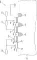
图2示出了可以由图1中所示的OTP存储单元100的电路表示的传统OTP存储单元200的截面图。FIG. 2 shows a cross-sectional view of a conventional
存储单元200可以包括列线208(COL)、可编程薄氧化物抗熔丝212、厚氧化物隔离件晶体管216、厚氧化物存取晶体管214和行线210(ROW)。这些元件分别对应于图1中的存储单元100中的列线108、可编程薄氧化物抗熔丝112、厚氧化物隔离件晶体管116、厚氧化物存取晶体管114和行线110。可编程薄氧化物抗熔丝212、厚氧化物隔离件晶体管216和厚氧化物存取晶体管214可以形成在基板202上。存储单元200还可以包括源极区224和漏极区222,源极区224和漏极区222是形成在基板202内的扩散区。
如图2所示,抗熔丝212可以靠近(例如,大致接近)隔离件晶体管216的一侧,而存取晶体管214的漏极区222可以靠近隔离件晶体管116的相对侧。尤其是,漏极区222可以是存取晶体管214的漏极并且还可以是隔离件晶体管216的源极。As shown in FIG. 2 ,
在本发明的示例性实施方式中,抗熔丝212包括基板202上的多晶硅层230和薄氧化层232。薄氧化层232可以具有例如大约20埃的厚度。In an exemplary embodiment of the invention, antifuse 212 includes
在本发明的示例性实施方式中,隔离件晶体管216包括多晶硅栅极234、厚氧化层236和漏极区222。厚氧化层236可以具有例如大约

在本发明的示例性实施方式中,存取晶体管214包括多晶硅栅极226、厚氧化层228、源极区224和漏极区222。多晶硅栅极226和厚氧化层228形成在基板202上,而源极区224和漏极区222是基板202中的扩散区。此外,厚氧化层228可以具有例如大约
虽然上述示例性实施方式的层230、栅极234和栅极226被描述成多晶硅,但不限于此材料,因为可以使用在不背离本发明的精神和范围的情况下对相关领域的技术人员来说显而易见的不同材料。在上述示例性实施方式中,基板202可以包括硅。然而,基板202的组成不限于硅且可以使用在不背离本发明的精神和范围的情况下对相关领域的技术人员来说显而易见的不同基板材料。Although
图3示出了根据本发明的示例性实施方式的一次性可编程(OTP)存储单元300的示例性电路。存储单元300类似于图1中所示的存储单元100,并且包括第二厚氧化物存取晶体管342。第二厚氧化物存取晶体管342为存储单元300提供额外电压保护的好处。FIG. 3 shows an exemplary circuit of a one-time programmable (OTP)
存储单元300可以包括列线308(COL)、可编程薄氧化物抗熔丝312、厚氧化物隔离件晶体管316、第一厚氧化物存取晶体管314、第二厚氧化物存取晶体管342、行线310(ROW)和输入端340。存储单元300基于抗熔丝312的状态存储一个比特的信息。存储单元300的状态基于抗熔丝312是“编程”(例如,抗熔丝312已经断裂)或是“未编程”(例如,抗熔丝312尚未断裂且保持开路)。存储单元300被制造为处于未编程状态并且只可以编程一次。即,一旦编程,存储单元300就无法恢复到未编程状态。
存储单元300可以通过将编程电压经由列线308施加给抗熔丝312和隔离件晶体管316的栅极,将第一电源电压经由行线310施加给第一厚氧化物存取晶体管314的栅极并将第二电源电压经由输入端340施加给第二厚氧化物存取晶体管342的栅极来编程。编程电压是幅值足够大以当列线308拉至接地时使抗熔丝312断裂的电压,并且例如可以是大于5V的电压。出于讨论目的,编程电压例如大约可以为5.4V。施加给第一厚氧化物存取晶体管314的栅极的第一电源电压例如大约为3.6V。施加给第二厚氧化物存取晶体管342的栅极的第二电源电压例如大约为1.8V。施加的电压不应限于此,且在不背离本发明的精神和范围的情况下可以是对相关领域的技术人员来说显而易见的任意电压,所述任意电压可以导致对存储单元300进行编程而不会导致损坏存储单元300和/或任意相邻存储单元。即,编程电压必须具有足够幅值以便在通过列线308施加时使抗熔丝312断裂,但不可以具有导致相邻存储单元的抗熔丝断裂的幅值。类似地,读取电压在读取操作期间通过列线308施加时不可以具有足够大以使相邻存储单元的抗熔丝断裂的幅值。
隔离件晶体管316的栅极上的编程电压充分导通晶体管并由此降低存取晶体管314的漏极与抗熔丝312之间的阻抗。置于第一和第二厚氧化物存取晶体管314和342的栅极上的电源电压充分导通晶体管并由此降低第一和第二厚氧化物存取晶体管314和342的源-漏阻抗。结果,抗熔丝312通过隔离件晶体管316,并通过第一和第二厚氧化物存取晶体管314和342耦接至地面。抗熔丝312上的所得电压电位足以使抗熔丝312断裂,从而将抗熔丝312置于低阻抗状态(例如,编程状态)下。The programming voltage on the gate of
存储单元300可以通过将例如大约1.1V至1.4V的读取电压施加给抗熔丝312,并将第二电源电压(例如,1.8V)分别经由行线310和输入端340施加给第一和第二厚氧化物存取晶体管314和342而被读取。第一和第二厚氧化物存取晶体管314和342的栅极上的电源电压充分导通晶体管并由此分别降低存取晶体管314和342的源-漏阻抗。类似地,隔离件晶体管316的栅极上的读取电压降低了隔离件晶体管316的阻抗。编程后的抗熔丝312由此通过隔离件晶体管316和存取晶体管314和342耦接至地面。The
如果抗熔丝312未被编程(例如,抗熔丝312为开路),并且因为抗熔丝312上的所得读取电压电位在读取过程中不足以使抗熔丝312断裂,列线308将保留在所施加的电压电位(例如,1.1V至1.4V),由此指示未编程状态。相反,如果抗熔丝312已经被编程,则列线308将通过隔离件晶体管316和存取晶体管314和342被拉至接地。因此,列线308上的电位将充分降至施加的读取电压以下以指示编程状态。具体地,列线308上的电位将降至隔离件晶体管316的切换阈值,在一个示例性实施方式中,该切换阈值大约可以为0.7V。If
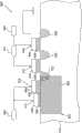
图4示出了本发明的示例性实施方式中的可以由图3中所示的OTP存储单元300的示例性电路表示的示例性OTP存储单元400的截面图。FIG. 4 shows a cross-sectional view of an exemplary
存储单元400可以包括列线408(COL)、可编程薄氧化物抗熔丝412、厚氧化物隔离件晶体管416、第一厚氧化物存取晶体管414、第二厚氧化物存取晶体管442、行线410(ROW)和输入端440。存储单元400基于抗熔丝412的状态存储一个比特的信息。这些元件分别对应于图3中的存储单元300中的列线308、可编程薄氧化物抗熔丝312、厚氧化物隔离件晶体管316、第一厚氧化物存取晶体管314、第二厚氧化物存取晶体管342、行线310和输入端340。可编程薄氧化物抗熔丝412、厚氧化物隔离件晶体管416和第一和第二厚氧化物存取晶体管414和442可以形成在基板402上。存储单元400还可以包括源极/漏极区422,424和448,源极/漏极区422,424和448是形成在基板202内的扩散区。
如图4所示,抗熔丝412可以靠近(例如,大致接近)隔离件晶体管416的一侧,而第一厚氧化物存取晶体管414的漏极区422可以靠近隔离件晶体管416的相对侧。尤其是,漏极区422可以用作存取晶体管414的漏极并且还可以用作隔离件晶体管416的源极。第一厚氧化物存取晶体管414可以相对于隔离件晶体管416靠近漏极区422的相对侧,而第一厚氧化物存取晶体管414的源极区424可以靠近厚氧化物存取晶体管414的相对侧。尤其是,源极区424可以用作第一厚氧化物存取晶体管414的源极并且还可以用作第二厚氧化物存取晶体管442的漏极。第二厚氧化物存取晶体管442的源极区448可以相对于厚氧化物存取晶体管442的漏极区424靠近厚氧化物存取晶体管442的相对侧。As shown in FIG. 4 ,
在本发明的示例性实施方式中,抗熔丝412包括形成在基板402上的多晶硅层430和薄氧化层432。薄氧化层432可以具有例如大约20埃
在本发明的示例性实施方式中,隔离件晶体管416包括多晶硅栅极434、厚氧化层436和漏极区422。厚氧化层436可以具有例如大约

在本发明的示例性实施方式中,第一厚氧化物存取晶体管414包括多晶硅栅极426、厚氧化层428、源极区424和漏极区422。多晶硅栅极426和厚氧化层428形成在基板402上,而源极区424和漏极区422是基板402中的扩散区。此外,厚氧化层428可以具有例如大约的厚度。In an exemplary embodiment of the invention, the first thick
在本发明的示例性实施方式中,第二厚氧化物存取晶体管442包括多晶硅栅极444、厚氧化层446、漏极区424和源极区448。多晶硅栅极444和厚氧化层446形成在基板402上,而漏极424和源极448是基板402中的扩散区。此外,厚氧化层446可以具有例如大约
虽然上述示例性实施方式的层430、栅极434、栅极426和栅极444包括多晶硅,但不限于此材料,且可以使用在不背离本发明的精神和范围的情况下对相关领域的技术人员来说显而易见的不同材料。在上述示例性实施方式中,基板402可以包括硅。然而,基板402的组成不限于硅且可以使用在不背离本发明的精神和范围的情况下对相关领域的技术人员来说显而易见的不同基板材料。Although
通过将隔离件晶体管416插入抗熔丝412与第一厚氧化物存取晶体管414之间有益地使存储单元400的编程实例的IV(电流-电压)特性更均匀。隔离件晶体管416确保薄氧化层432的断裂部位与漏极区422之间的最小距离。不管断裂部位是出现在薄氧化层432的一侧450上还是相对于隔离件晶体管416出现在薄氧化层432的相对侧452上,由隔离件晶体管416强加的至漏极区422的额外缓冲距离明显降低了由此产生的断裂部位的位置的影响,并因此增加编程存储单元400的IV特性的均匀性。换句话说,隔离件晶体管416的横向距离降低了可能改变断裂部位的位置的影响。此外,第二厚氧化物存取晶体管442的增设提供增加电压保护的好处。IV特性和电压保护的改善会导致存储单元400的编程确定性和寿命增加。Inserting
图5示出了根据本发明的示例性实施方式的示例性OTP存储单元500的截面图。OTP存储单元500类似于存储单元400,但包括原生掺杂区域(Natively-doped region)550。FIG. 5 shows a cross-sectional view of an exemplary
除了原生掺杂区域550之外,存储单元500还可以包括列线508(COL)、可编程薄氧化物抗熔丝512、厚氧化物隔离件晶体管516、第一厚氧化物存取晶体管514、第二厚氧化物存取晶体管542、行线510(ROW)和输入端540。这些元件分别对应于图4中的列线408、可编程薄氧化物抗熔丝412、厚氧化物隔离件晶体管416、第一厚氧化物存取晶体管414、第二厚氧化物存取晶体管442、行线410和输入端440。因此,已经省略这些类似元件的描述。In addition to the natively doped
原生掺杂区域550是基板502的覆盖有原生注入掩膜的区域,并因此没有受到通常对基板502执行的注入处理的区域(例如,原生掺杂区域550是基板502的非掺杂区域)。换句话说,原生掺杂区域550可以是基板502的非掺杂区域,而基板502的未覆盖有原生注入掩膜的区域受到了注入处理(即,这些其他区域是掺杂区域)。原生掺杂区域550位于基板502的其上形成有可编程薄氧化物抗熔丝512和厚氧化物隔离件晶体管516的区域中下方。即,可编程薄氧化物抗熔丝512和厚氧化物隔离件晶体管516设置在基板502的原生掺杂区域550上。更具体地,可编程薄氧化物抗熔丝512和厚氧化物隔离件晶体管516设置在基板502的表面上,以便位于由原生掺杂区域550限定的区域“印记(footprint)”之内。如图5所示,原生掺杂区域550可以延伸超过基板502的在可编程薄氧化物抗熔丝512和厚氧化物隔离件晶体管516正下方的区域。例如,原生掺杂区域550可以延伸为包括漏极522的一部分。另外地或可选地,原生掺杂区域550可以延伸为包括基板502的超过与厚氧化物隔离件晶体管516相对的可编程薄氧化物抗熔丝512的一侧的部分,如边缘552所示。Natively
基板502的没有包括在原生掺杂区域550中的区域可以利用标准阈值电压注入过程来掺杂,在不背离本发明的精神和范围的情况下这对相关领域的技术人员来说是显而易见的。例如,基板502的没有包括早原生掺杂区域550中的区域可以进行掺杂注入处理,从而为这些区域产生标准阈值电压特性。Regions of
通过包括原生掺杂区域550有益地使存储单元500的编程实例的IV(电流-电压)特性更均匀。具体地,原生掺杂区域550,及其设置,提供存储单元500的更均匀的阈值和反向击穿电压。The IV (current-voltage) characteristics of the programmed instances of
图6示出了在本发明的示例性实施方式中受到编程处理的包括示例性OTP存储器601的示例性OTP存储单元阵列600。存储单元601类似于图3至图5中所示的示例性存储单元,其包括第二厚氧化物存取晶体管(例如,图5的第二厚氧化物存取晶体管542)。要注意的是,为了便于示出,抗熔丝612和隔离件晶体管616在图6中被表示为单个组件612/616。FIG. 6 illustrates an exemplary OTP
在编程操作期间,施加给存储单元阵列内的每个存储单元的各个组件的电压的组合,或缺少电压,确定当前编程存储单元。例如,为了编程存储单元阵列的存储单元601,编程电压(例如,大约5.4V)通过列线608施加给隔离件晶体管616的栅极和抗熔丝612,第一电源电压(例如,大约3.6V)通过行线610施加给第一厚氧化物存取晶体管614的栅极,第二电源电压(大约1.8V)通过输入端640施加给第二厚氧化物存取晶体管642的栅极,并且第二厚氧化物存取晶体管642的源极648被拉至接地。During a programming operation, the combination of voltages, or lack thereof, applied to various components of each memory cell within the memory cell array determines the currently programmed memory cell. For example, to program
要注意的是,存储单元阵列600的与存储单元601位于同一行内的其他存储单元也将具有施加给其各个隔离件晶体管和抗熔丝的相似电压,以及至其各个第一和第二厚氧化物存取晶体管的相似电压。然而,编程行中的这些其他存储单元没有受到编程处理,原因是其各个第二厚氧化物存取晶体管的源极被拉至第二电源电压(例如,1.8V)而不是被拉至接地。It is to be noted that other memory cells of
类似地,与存储单元601同一行中的各个存储单元的每一个的第二厚氧化物存取晶体管的源极也将被拉至接地。然而,编程列中的这些其他存储单元没有受到编程处理,原因是在这些存储单元的每一个中,隔离件晶体管的栅极、抗熔丝、第一厚氧化物存取晶体管的栅极和第二厚氧化物存取晶体管的栅极被拉至接地而不是拉至编程电压和电源电压。Similarly, the source of the second thick oxide access transistor of each of the memory cells in the same row as
图7示出了在本发明的示例性实施方式中受到读取操作的包括示例性OTP存储单元701的示例性OTP存储单元阵列700。存储单元701类似于图3至图6中所示的示例性存储单元,其包括第二厚氧化物存取晶体管。要注意的是,为了便于示出,抗熔丝712和隔离件晶体管716在图7中被表示为单个组件712/716。FIG. 7 illustrates an exemplary OTP
在读取操作期间,施加给存储单元阵列内的每个存储单元的各个组件的电压的组合,或缺少电压,确定当前读取存储单元。例如,为了读取存储单元阵列的存储单元701,读取电压(例如,大约1.1V至1.4V)通过列线708施加给隔离件晶体管716的栅极和抗熔丝712,第二电源电压(例如,大约1.8V)通过行线710施加给第一厚氧化物存取晶体管714的栅极并通过输入端740施加给第二厚氧化物存取晶体管742的栅极,并且第二厚氧化物存取晶体管742的源极748被拉至接地。During a read operation, a combination of voltages, or lack thereof, applied to various components of each memory cell within the array of memory cells determines the memory cell that is currently being read. For example, to read
要注意的是,存储单元阵列700的与存储单元701位于同一行内的其他存储单元也将具有施加给其各个隔离件晶体管和抗熔丝的相似电压,以及至其各个第一和第二厚氧化物存取晶体管的相似电压。然而,读取行中的这些其他存储单元没有被读取,原因是其各个第二厚氧化物存取晶体管的源极被拉至第二电源电压(例如,1.8V)而不是被拉至接地。It is to be noted that other memory cells of
类似地,与存储单元700同一行中的各个存储单元的每一个的第二厚氧化物存取晶体管的源极也将拉至接地。然而,读取列中的这些其他存储单元没有被读取,原因是在这些存储单元的每一个的隔离件晶体管的栅极、抗熔丝、第一厚氧化物存取晶体管的栅极和第二厚氧化物存取晶体管的栅极被拉至接地而不是被拉至读取电压和电源电压。此外,如图7所示,读取行中的没有被读取的存储单元也可以具有施加给第一厚氧化物存取晶体管的栅极的第二电源电压,同时第二晶体管的栅极被拉至接地(例如,第二存取晶体管断开)。Similarly, the source of the second thick oxide access transistor of each of the memory cells in the same row as
上文在示出了实现指定功能及其关系的功能构建块的帮助下对本发明进行了描述。为了便于描述,本文任意限定了功能构建块的范围。只要适当执行指定功能及其关系就可以限定替代范围。The invention has been described above with the aid of functional building blocks illustrating specified functions and relationships thereof. The scope of functional building blocks has been arbitrarily limited herein for convenience of description. Alternate ranges may be defined so long as the specified functions and relationships thereof are appropriately performed.
在说明书中对“一个实施方式”、“某一实施方式”、“示例性实施方式”的参考表明所描述的实施方式可以包括特定特征、结构或特性,但每个实施方式不一定包括所述特定特征、结构或特性。此外,这样措辞不一定参考相同实施方式。此外,当结合实施方式描述特定特征、结构或特性时,提出在本领域技术人员的知识范围内以便结合其他实施方式来影响此特征、结构或特性,无论是否明确描述。References in the specification to "one embodiment," "an embodiment," and "exemplary embodiment" indicate that the described embodiments may include particular features, structures, or characteristics, but that each embodiment does not necessarily include the described embodiments. A specific feature, structure, or characteristic. Moreover, such terms are not necessarily referring to the same embodiment. Furthermore, when a particular feature, structure or characteristic is described in connection with an embodiment, it is suggested that it is within the knowledge of those skilled in the art to affect that feature, structure or characteristic in conjunction with other embodiments whether explicitly described or not.
实施方式可以在硬件(例如,电路)、固件、软件或其任意组合中被实现。实施方式还可以实现为存储在机器可读介质上的指令,所述指令可以由一个或多个处理器读取并执行。机器可读介质可以包括存储或传输呈机器(例如计算设备)可读的形式的信息的任何机构。例如,机器可读介质可以包括只读存储器(ROM)、随机存取存储器(RAM)、磁盘存储介质、光学存储介质、闪存设备、电、光、声或其他形式的传播信号(例如,载波、红外线信号、数字信号等)等。此外,固件、软件、例程、指令在本文中可以被描述成执行某些操作。然而,应理解,这样的描述仅仅是为了方便起见,这样的操作实际上是由计算设备、处理器、控制器或执行固件、软件、例程、指令等的其他设备引起的。此外,实现变更中的任意实现变更可以由通用计算机来执行。Embodiments may be implemented in hardware (eg, circuits), firmware, software, or any combination thereof. Embodiments can also be implemented as instructions stored on a machine-readable medium, which can be read and executed by one or more processors. A machine-readable medium may include any mechanism for storing or transmitting information in a form readable by a machine (eg, a computing device). For example, a machine-readable medium may include read-only memory (ROM), random-access memory (RAM), magnetic disk storage media, optical storage media, flash memory devices, electrical, optical, acoustic, or other forms of propagated signals (e.g., carrier waves, infrared signal, digital signal, etc.), etc. Furthermore, firmware, software, routines, instructions may be described herein as performing certain operations. However, it should be understood that such description is for convenience only and that such operations are actually caused by the computing device, processor, controller, or other device executing firmware, software, routines, instructions, or the like. In addition, any of the implementation changes can be performed by a general-purpose computer.
本文描述的示例性实施方式用于说明目的,而不是限制性的。其他示例性实施方式是可能的,且在本发明的精神和范围内可以对示例性实施方式进行修改。因此,本说明书并不意味着限制本发明或权利要求。此外,仅根据以下权利要求及其等同物来确定本发明的范围。The exemplary embodiments described herein are for purposes of illustration and not limitation. Other exemplary embodiments are possible, and modifications may be made to the exemplary embodiments within the spirit and scope of the invention. Accordingly, the description is not meant to limit the invention or the claims. Furthermore, the scope of the present invention is to be determined only by the following claims and their equivalents.
示例性实施方式的前述具体实施方式揭示本发明的一般性,使得在不背离本发明的精神和范围的情况下,可以通过应用相关领域的技术人员的知识,对各种应用比如示例性实施方式进行轻易的修改和/或改动,而无需进行不合理的实验。因此,根据本文提出的教义和指导,这样的改动和修改的目的在该含义和多个示例性实施方式的等同物之内。应理解,本文的措辞或术语的目的是描述,而不是限制,因此本说明书的术语或措辞必须由相关领域的技术人员根据本文的教义进行解释。The foregoing detailed description of the exemplary embodiments reveals the generality of the invention such that various applications such as the exemplary embodiments can be applied by applying the knowledge of those skilled in the relevant art without departing from the spirit and scope of the invention. Make light modifications and/or changes without unreasonable experimentation. Therefore, such adaptations and modifications are intended to be within the meaning and equivalents of the various exemplary embodiments, based on the teaching and guidance presented herein. It should be understood that the purpose of the phrases or terms herein is description, not limitation, and therefore the terms or phrases in this specification must be interpreted by those skilled in the relevant art in accordance with the teachings herein.
结论in conclusion
应理解,具体实施方式部分(而不是摘要部分)旨在用于对权利要求进行解释。摘要部分可以描述一个或多个示例性实施方式,但并不是所有示例性实施方式,因此,并非旨在以任何方式对本发明和所附权利要求进行限制。It should be understood that the Detailed Description section, and not the Abstract section, is intended for interpretation of the claims. The Abstract may describe one or more, but not all, exemplary embodiments and, therefore, is not intended to limit the invention and the appended claims in any way.
对相关领域的技术人员来说显而易见的是,在不背离本发明的精神和范围的情况下,在本发明中,可以对形式和细节进行各种改变。因此,本发明不应限于上述示例性实施方式中的任何一个,而仅根据以下权利要求及其等同物进行限定。It will be apparent to those skilled in the relevant art that various changes in form and details can be made in the present invention without departing from the spirit and scope of the invention. Accordingly, the invention should not be limited to any of the above-described exemplary embodiments, but only in accordance with the following claims and their equivalents.
Claims (10)
Applications Claiming Priority (2)
| Application Number | Priority Date | Filing Date | Title |
|---|---|---|---|
| US13/608,595 | 2012-09-10 | ||
| US13/608,595US9136217B2 (en) | 2012-09-10 | 2012-09-10 | One-time programmable memory cell |
Publications (2)
| Publication Number | Publication Date |
|---|---|
| CN103680633Atrue CN103680633A (en) | 2014-03-26 |
| CN103680633B CN103680633B (en) | 2017-10-31 |
Family
ID=48985941
Family Applications (2)
| Application Number | Title | Priority Date | Filing Date |
|---|---|---|---|
| CN201320555215.0UExpired - LifetimeCN203456098U (en) | 2012-09-10 | 2013-09-06 | Programmable storage unit |
| CN201310404318.1AExpired - Fee RelatedCN103680633B (en) | 2012-09-10 | 2013-09-06 | One-time programmable memory cell |
Family Applications Before (1)
| Application Number | Title | Priority Date | Filing Date |
|---|---|---|---|
| CN201320555215.0UExpired - LifetimeCN203456098U (en) | 2012-09-10 | 2013-09-06 | Programmable storage unit |
Country Status (4)
| Country | Link |
|---|---|
| US (1) | US9136217B2 (en) |
| EP (1) | EP2706571A2 (en) |
| CN (2) | CN203456098U (en) |
| TW (1) | TWI538105B (en) |
Cited By (2)
| Publication number | Priority date | Publication date | Assignee | Title |
|---|---|---|---|---|
| CN104966532A (en)* | 2014-06-30 | 2015-10-07 | 成都芯源系统有限公司 | One-time programmable memory unit and circuit |
| TWI870843B (en)* | 2023-04-21 | 2025-01-21 | 香港商艾元創新有限公司 | Memory device, integrated circuit and manufacturing method of the same |
Families Citing this family (4)
| Publication number | Priority date | Publication date | Assignee | Title |
|---|---|---|---|---|
| US9136217B2 (en)* | 2012-09-10 | 2015-09-15 | Broadcom Corporation | One-time programmable memory cell |
| US9799662B2 (en) | 2015-08-18 | 2017-10-24 | Ememory Technology Inc. | Antifuse-type one time programming memory cell and array structure with same |
| US9627016B2 (en)* | 2015-09-10 | 2017-04-18 | Cypress Semiconductor Corporation | Systems, methods, and devices for parallel read and write operations |
| US10109364B2 (en)* | 2015-10-21 | 2018-10-23 | Avago Technologies General Ip (Singapore) Pte. Ltd. | Non-volatile memory cell having multiple signal pathways to provide access to an antifuse of the memory cell |
Citations (5)
| Publication number | Priority date | Publication date | Assignee | Title |
|---|---|---|---|---|
| US20060291267A1 (en)* | 2005-06-28 | 2006-12-28 | Jenne Fredrick B | Antifuse circuit with current regulator for controlling programming current |
| CN101393932A (en)* | 2007-09-19 | 2009-03-25 | 恩益禧电子股份有限公司 | non-volatile semiconductor storage device |
| US20090237975A1 (en)* | 2008-03-21 | 2009-09-24 | Broadcom Corporation | One-time programmable memory cell |
| CN102612717A (en)* | 2009-10-30 | 2012-07-25 | 赛鼎矽公司 | Twin well split-channel otp memory cell |
| CN203456098U (en)* | 2012-09-10 | 2014-02-26 | 美国博通公司 | Programmable storage unit |
Family Cites Families (3)
| Publication number | Priority date | Publication date | Assignee | Title |
|---|---|---|---|---|
| US6836000B1 (en) | 2000-03-01 | 2004-12-28 | Micron Technology, Inc. | Antifuse structure and method of use |
| KR100500579B1 (en) | 2003-06-28 | 2005-07-12 | 한국과학기술원 | 3-Transistor OTP ROM using CMOS Gate Oxide Antifuse |
| US7206247B2 (en)* | 2005-06-28 | 2007-04-17 | Cypress Semiconductor Corporation | Antifuse circuit with dynamic current limiter |
- 2012
- 2012-09-10USUS13/608,595patent/US9136217B2/enactiveActive
- 2013
- 2013-08-14EPEP20130004055patent/EP2706571A2/ennot_activeWithdrawn
- 2013-08-28TWTW102130785Apatent/TWI538105B/ennot_activeIP Right Cessation
- 2013-09-06CNCN201320555215.0Upatent/CN203456098U/ennot_activeExpired - Lifetime
- 2013-09-06CNCN201310404318.1Apatent/CN103680633B/ennot_activeExpired - Fee Related
Patent Citations (5)
| Publication number | Priority date | Publication date | Assignee | Title |
|---|---|---|---|---|
| US20060291267A1 (en)* | 2005-06-28 | 2006-12-28 | Jenne Fredrick B | Antifuse circuit with current regulator for controlling programming current |
| CN101393932A (en)* | 2007-09-19 | 2009-03-25 | 恩益禧电子股份有限公司 | non-volatile semiconductor storage device |
| US20090237975A1 (en)* | 2008-03-21 | 2009-09-24 | Broadcom Corporation | One-time programmable memory cell |
| CN102612717A (en)* | 2009-10-30 | 2012-07-25 | 赛鼎矽公司 | Twin well split-channel otp memory cell |
| CN203456098U (en)* | 2012-09-10 | 2014-02-26 | 美国博通公司 | Programmable storage unit |
Cited By (4)
| Publication number | Priority date | Publication date | Assignee | Title |
|---|---|---|---|---|
| CN104966532A (en)* | 2014-06-30 | 2015-10-07 | 成都芯源系统有限公司 | One-time programmable memory unit and circuit |
| CN104966532B (en)* | 2014-06-30 | 2018-10-30 | 成都芯源系统有限公司 | One-time programmable memory unit and circuit |
| TWI870843B (en)* | 2023-04-21 | 2025-01-21 | 香港商艾元創新有限公司 | Memory device, integrated circuit and manufacturing method of the same |
| US12439591B2 (en) | 2023-04-21 | 2025-10-07 | Ipcell Corporation Limited | Memory device, integrated circuit and manufacturing method of the same |
Also Published As
| Publication number | Publication date |
|---|---|
| US20140071731A1 (en) | 2014-03-13 |
| TWI538105B (en) | 2016-06-11 |
| US9136217B2 (en) | 2015-09-15 |
| CN103680633B (en) | 2017-10-31 |
| CN203456098U (en) | 2014-02-26 |
| TW201415581A (en) | 2014-04-16 |
| EP2706571A2 (en) | 2014-03-12 |
Similar Documents
| Publication | Publication Date | Title |
|---|---|---|
| CN103680633B (en) | One-time programmable memory cell | |
| US9324381B2 (en) | Antifuse OTP memory cell with performance improvement, and manufacturing method and operating method of memory | |
| US9601499B2 (en) | One-time programmable memory cell capable of reducing leakage current and preventing slow bit response, and method for programming a memory array comprising the same | |
| KR101289213B1 (en) | Antifuse programmable memory array | |
| CN101800083B (en) | FinFET fuse operation method and integrated circuit structure | |
| CN102376358B (en) | Electronic system, antifuse memory element and method for providing the same | |
| US9281074B2 (en) | One time programmable memory cell capable of reducing leakage current and preventing slow bit response | |
| TWI496154B (en) | One-bit memory cell for nonvolatile memory | |
| US7102951B2 (en) | OTP antifuse cell and cell array | |
| KR101144218B1 (en) | Split-channel antifuse array architecture | |
| US8031506B2 (en) | One-time programmable memory cell | |
| KR20120020272A (en) | Antifuse memory cell, manufacturing method of the same, non-volatile memory device and memory device with repair function having the same | |
| JP2009503901A (en) | One-time programmable memory and method of operating the same | |
| US20050276105A1 (en) | Nand-type non-volatile memory cell and method for operating same | |
| CN106783858B (en) | A Layout Structure of Gate Oxide Antifuse PROM Memory Cell | |
| EP2439746A1 (en) | Single polysilicon non-volatile memory | |
| KR20180018881A (en) | OTP Cell Having Improved Programming Reliability | |
| US9424926B2 (en) | Reduced size semiconductor device and method for manufacture thereof | |
| HK1191725A (en) | One-time programmable memory cell | |
| US20160307636A1 (en) | Method and apparatus for improving data retention and read-performance of a non-volatile memory device | |
| US10127980B2 (en) | Integrated circuit including memory, and write method | |
| JP2010027154A (en) | Method of writing data to semiconductor device, and semiconductor device | |
| KR20120048094A (en) | Fuse of semiconductor device |
Legal Events
| Date | Code | Title | Description |
|---|---|---|---|
| PB01 | Publication | ||
| PB01 | Publication | ||
| C10 | Entry into substantive examination | ||
| SE01 | Entry into force of request for substantive examination | ||
| REG | Reference to a national code | Ref country code:HK Ref legal event code:DE Ref document number:1191725 Country of ref document:HK | |
| TA01 | Transfer of patent application right | Effective date of registration:20170328 Address after:Singapore Singapore Applicant after:Avago Technologies Fiber IP Singapore Pte. Ltd. Address before:American California Applicant before:Zyray Wireless Inc. | |
| TA01 | Transfer of patent application right | ||
| GR01 | Patent grant | ||
| GR01 | Patent grant | ||
| TR01 | Transfer of patent right | Effective date of registration:20181101 Address after:Singapore Singapore Patentee after:Annwa high tech Limited by Share Ltd Address before:Singapore Singapore Patentee before:Avago Technologies Fiber IP Singapore Pte. Ltd. | |
| TR01 | Transfer of patent right | ||
| CF01 | Termination of patent right due to non-payment of annual fee | Granted publication date:20171031 Termination date:20180906 | |
| CF01 | Termination of patent right due to non-payment of annual fee | ||
| REG | Reference to a national code | Ref country code:HK Ref legal event code:WD Ref document number:1191725 Country of ref document:HK |