CN103680628A - Semiconductor memory device - Google Patents
Semiconductor memory deviceDownload PDFInfo
- Publication number
- CN103680628A CN103680628ACN201310047336.9ACN201310047336ACN103680628ACN 103680628 ACN103680628 ACN 103680628ACN 201310047336 ACN201310047336 ACN 201310047336ACN 103680628 ACN103680628 ACN 103680628A
- Authority
- CN
- China
- Prior art keywords
- line
- sub
- bit
- bit line
- door
- Prior art date
- Legal status (The legal status is an assumption and is not a legal conclusion. Google has not performed a legal analysis and makes no representation as to the accuracy of the status listed.)
- Granted
Links
- 239000004065semiconductorSubstances0.000titleclaimsabstractdescription38
- 239000000872bufferSubstances0.000claimsdescription29
- 230000004044responseEffects0.000claimsdescription26
- 230000006870functionEffects0.000claimsdescription14
- 230000008878couplingEffects0.000claims2
- 238000010168coupling processMethods0.000claims2
- 238000005859coupling reactionMethods0.000claims2
- 238000010586diagramMethods0.000description16
- 238000012546transferMethods0.000description15
- 230000002093peripheral effectEffects0.000description8
- 230000005540biological transmissionEffects0.000description6
- 101000741396Chlamydia muridarum (strain MoPn / Nigg) Probable oxidoreductase TC_0900Proteins0.000description5
- 101000741399Chlamydia pneumoniae Probable oxidoreductase CPn_0761/CP_1111/CPj0761/CpB0789Proteins0.000description5
- 101000741400Chlamydia trachomatis (strain D/UW-3/Cx) Probable oxidoreductase CT_610Proteins0.000description5
- 102100029469WD repeat and HMG-box DNA-binding protein 1Human genes0.000description5
- 101710097421WD repeat and HMG-box DNA-binding protein 1Proteins0.000description5
- 238000012795verificationMethods0.000description4
- 230000004927fusionEffects0.000description3
- 238000005516engineering processMethods0.000description2
- 238000012986modificationMethods0.000description2
- 230000004048modificationEffects0.000description2
- 238000012545processingMethods0.000description2
- 238000013403standard screening designMethods0.000description2
- 238000003491arrayMethods0.000description1
- 238000012937correctionMethods0.000description1
- 238000013461designMethods0.000description1
- 230000000694effectsEffects0.000description1
- PWPJGUXAGUPAHP-UHFFFAOYSA-NlufenuronChemical compoundC1=C(Cl)C(OC(F)(F)C(C(F)(F)F)F)=CC(Cl)=C1NC(=O)NC(=O)C1=C(F)C=CC=C1FPWPJGUXAGUPAHP-UHFFFAOYSA-N0.000description1
- 238000000034methodMethods0.000description1
- 239000007787solidSubstances0.000description1
Images


Classifications
- G—PHYSICS
- G11—INFORMATION STORAGE
- G11C—STATIC STORES
- G11C7/00—Arrangements for writing information into, or reading information out from, a digital store
- G11C7/12—Bit line control circuits, e.g. drivers, boosters, pull-up circuits, pull-down circuits, precharging circuits, equalising circuits, for bit lines
- G—PHYSICS
- G11—INFORMATION STORAGE
- G11C—STATIC STORES
- G11C16/00—Erasable programmable read-only memories
- G11C16/02—Erasable programmable read-only memories electrically programmable
- G11C16/06—Auxiliary circuits, e.g. for writing into memory
- G11C16/10—Programming or data input circuits
- G11C16/12—Programming voltage switching circuits
- G—PHYSICS
- G11—INFORMATION STORAGE
- G11C—STATIC STORES
- G11C16/00—Erasable programmable read-only memories
- G11C16/02—Erasable programmable read-only memories electrically programmable
- G11C16/06—Auxiliary circuits, e.g. for writing into memory
- G11C16/24—Bit-line control circuits
- G—PHYSICS
- G11—INFORMATION STORAGE
- G11C—STATIC STORES
- G11C7/00—Arrangements for writing information into, or reading information out from, a digital store
- G11C7/10—Input/output [I/O] data interface arrangements, e.g. I/O data control circuits, I/O data buffers
- G—PHYSICS
- G11—INFORMATION STORAGE
- G11C—STATIC STORES
- G11C8/00—Arrangements for selecting an address in a digital store
- G—PHYSICS
- G11—INFORMATION STORAGE
- G11C—STATIC STORES
- G11C8/00—Arrangements for selecting an address in a digital store
- G11C8/12—Group selection circuits, e.g. for memory block selection, chip selection, array selection
Landscapes
- Engineering & Computer Science (AREA)
- Microelectronics & Electronic Packaging (AREA)
- Read Only Memory (AREA)
Abstract
Translated fromChineseDescription
Translated fromChinese相关申请的交叉引用Cross References to Related Applications
本申请要求2012年8月29日提交的申请号为10-2012-0095051的韩国专利申请的优先权,其全部内容通过引用合并于此。This application claims priority from Korean Patent Application No. 10-2012-0095051 filed on Aug. 29, 2012, the entire contents of which are hereby incorporated by reference.
技术领域technical field
本发明的示例性实施例涉及一种半导体设计技术,更具体而言,涉及一种包括位线的半导体存储器件。Exemplary embodiments of the present invention relate to a semiconductor design technology, and more particularly, to a semiconductor memory device including bit lines.
背景技术Background technique
半导体存储器件包括存储器阵列。存储器阵列中包括的存储器单元可以分成存储块。为了执行与输入至存储器单元和从存储器单元输出的数据相关的操作,应将数据输入/输出操作所需的操作电压提供给选中的存储块。Semiconductor memory devices include memory arrays. Memory cells included in a memory array may be divided into memory blocks. In order to perform operations related to data input to and output from the memory cells, an operation voltage required for data input/output operations should be supplied to selected memory blocks.
为了将操作电压提供给存储块中的选中的存储块,需要行译码器和电压传送电路,行译码器用于根据行地址信号来产生块选择信号,电压传送电路用于根据块选择信号而将操作电压传送给选中的存储块。In order to provide an operating voltage to a selected memory block in the memory blocks, a row decoder and a voltage transmission circuit are required, the row decoder is used to generate a block selection signal according to the row address signal, and the voltage transmission circuit is used to generate a block selection signal according to the block selection signal. Deliver the operating voltage to the selected memory block.
由于存储器阵列包括多个存储块,因此应产生与存储块的数目相对应的块选择信号来选择这些存储块中的一个。因此,用于实现行译码器的电路变得复杂,并且增大了行译码器所占据的面积。Since the memory array includes a plurality of memory blocks, a block selection signal corresponding to the number of memory blocks should be generated to select one of the memory blocks. Therefore, the circuit for realizing the row decoder becomes complicated, and the area occupied by the row decoder increases.
为了输入数据到存储器单元/从存储器单元输出数据,可能需要高电压。因此,电压传送电路应具有能够以高电压操作的高电压晶体管。高电压晶体管的尺寸比正常晶体管的尺寸大得多。由于每个存储块被设置有电压传送电路,因此电压传送电路所占据的面积相当成负担。In order to input/output data to/from a memory cell, a high voltage may be required. Therefore, the voltage transfer circuit should have high voltage transistors capable of operating at high voltage. High voltage transistors are much larger in size than normal transistors. Since each memory block is provided with a voltage transfer circuit, the area occupied by the voltage transfer circuit is quite burdensome.
结果,外围电路所占据的面积相应地随着存储块的数目的增多而相应地增大,由此芯片尺寸也增大。As a result, the area occupied by the peripheral circuits correspondingly increases as the number of memory blocks increases, whereby the chip size also increases.
发明内容Contents of the invention
本发明的示例性实施例提供一种防止外围电路所占据的面积增大的半导体存储器件。Exemplary embodiments of the present invention provide a semiconductor memory device that prevents an increase in the area occupied by peripheral circuits.
根据本发明的一个实施例,一种半导体存储器件包括:第一存储块组,所述第一存储块组包括与第一子位线耦接的存储块;第二存储块组,所述第二存储块组包括与第二子位线耦接的存储块;操作电路,所述操作电路与主位线耦接并且被配置为执行选自第一存储块组或第二存储块组的存储块的数据输入/输出操作;以及位线控制电路,所述位线控制电路被配置为响应于用于选择第一存储块组和第二存储块组中的包括选中的存储块的存储块组的组选择信号,以及由操作电路控制的主位线的电压,来不同地控制选中的存储块组的子位线和未选中的存储块组的子位线。According to an embodiment of the present invention, a semiconductor memory device includes: a first memory block group, the first memory block group includes memory blocks coupled to first sub-bit lines; a second memory block group, the first The two memory block groups include memory blocks coupled to the second sub-bit line; an operating circuit coupled to the main bit line and configured to perform storage selected from the first memory block group or the second memory block group a data input/output operation of a block; and a bit line control circuit configured to respond to a selection of a memory block group including a selected memory block among the first memory block group and the second memory block group The sub-bit lines of the selected memory block group and the sub-bit lines of the unselected memory block group are controlled differently by the group selection signal of the group selection signal and the voltage of the main bit line controlled by the operation circuit.
在本发明的实施例中,可以防止外围电路所占据的面积增大。In the embodiments of the present invention, an increase in the area occupied by peripheral circuits can be prevented.
附图说明Description of drawings
结合附图考虑并参考以下具体描述,本发明的上述和其它的特点和优点将变得更加明显:The above and other features and advantages of the present invention will become more apparent when considered in conjunction with the accompanying drawings and with reference to the following detailed description:
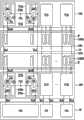
图1是说明根据本发明的一个实施例的半导体存储器件的框图;FIG. 1 is a block diagram illustrating a semiconductor memory device according to one embodiment of the present invention;
图2是说明图1所示的存储块的详细图;Figure 2 is a detailed diagram illustrating the memory block shown in Figure 1;
图3是说明图1所示的电压提供电路的详细图;FIG. 3 is a detailed diagram illustrating the voltage supply circuit shown in FIG. 1;
图4是说明图1所示的位线控制电路的详细图;FIG. 4 is a detailed diagram illustrating the bit line control circuit shown in FIG. 1;
图5是说明图1所示的位线控制电路的连接的详细图;FIG. 5 is a detailed diagram illustrating the connection of the bit line control circuit shown in FIG. 1;
图6是示意性地说明包括根据本发明的实施例的半导体存储器件的存储系统的框图;6 is a block diagram schematically illustrating a memory system including a semiconductor memory device according to an embodiment of the present invention;
图7是示意性地说明用于执行根据上述实施例的编程操作的融合式存储器件或融合式存储系统的框图;以及7 is a block diagram schematically illustrating a fused memory device or a fused memory system for performing a programming operation according to the above-described embodiments; and
图8是示意性地说明包括根据本发明的实施例的半导体存储器件的计算系统的框图。FIG. 8 is a block diagram schematically illustrating a computing system including a semiconductor memory device according to an embodiment of the present invention.
具体实施方式Detailed ways
在下文中,将参照附图详细地描述本发明的优选实施例。尽管结合若干说明性的实施例来描述实施例,但是应当理解的是,本领域技术人员可以设想出将落入本公开原理的精神和范围内的多种其它变型和实施例。在本说明书中,“连接/耦接”表示一个部件与另一个部件直接耦接或经由另一个部件间接耦接。在本说明书中,只要不在句子中特意提及,单数形式可以包括复数形式。Hereinafter, preferred embodiments of the present invention will be described in detail with reference to the accompanying drawings. Although embodiments have been described in conjunction with a number of illustrative embodiments thereof, it should be understood that numerous other modifications and embodiments can be devised by those skilled in the art that will fall within the spirit and scope of the principles of this disclosure. In this specification, "connected/coupled" means that one component is directly coupled with another component or indirectly coupled via another component. In this specification, a singular form may include a plural form as long as it is not specifically mentioned in a sentence.
图1是说明根据本发明的一个实施例的半导体存储器件的框图。FIG. 1 is a block diagram illustrating a semiconductor memory device according to one embodiment of the present invention.
在图1中,半导体存储器件包括存储器阵列110和外围电路120至170。外围电路包括操作电路120、130、140、160和170以及位线控制电路150。在快闪存储器件中,操作电路可以包括控制电路120、电压提供电路130、页缓冲器组140、列选择电路160和输入/输出电路170。In FIG. 1 , a semiconductor memory device includes a
存储器阵列110包括存储块组110PA和110PB。存储块组110PA和110PB具有存储块110MB。第一存储块组110PA中的存储块110MB与第一子位线BLe0A至BLekA耦接,第二存储块组110PB中的存储块110MB与第二子位线BLo0B至BLokB耦接。这里,第一存储块组110PA可以是第一存储平面(plane),第二存储块组110PB可以是第二存储平面。
在下文中,将详细描述存储块组110PA和110PB中包括的存储块110MB。Hereinafter, the memory block 110MB included in the memory block groups 110PA and 110PB will be described in detail.
图2是说明图1所示的存储块的详细图。将通过第二存储块组110PB中包括的存储块110MB来详细地描述存储块的操作。FIG. 2 is a detailed diagram illustrating a memory block shown in FIG. 1 . The operation of the memory block will be described in detail through the memory block 110MB included in the second memory block group 110PB.
在图2中,每个存储块包括耦接在位线BLe0B至BLekB和BLo0B至BLokB与公共源极线SL之间的存储串ST。即,存储串ST与相应的位线BLe0B至BLekB和BLo0B至BLokB耦接,并且它们与公共源极线SL耦接。这里,描述的位线BLe0B至BLekB和BLo0B至BLokB是第二子位线BLe0B至BLekB和BLo0B至BLokB。In FIG. 2, each memory block includes a string ST coupled between bit lines BLe0B to BLekB and BLo0B to BLokB and a common source line SL. That is, the string ST is coupled to the corresponding bit lines BLe0B to BLekB and BLo0B to BLokB, and they are coupled to the common source line SL. Here, the described bit lines BLe0B to BLekB and BLo0B to BLokB are the second sub bit lines BLe0B to BLekB and BLo0B to BLokB.
每个存储串ST包括源极选择晶体管SST、存储器单元Ce00至Cen0串联耦接成的单元串、以及漏极选择晶体管DST。源极选择晶体管SST的源极与公共源极线SL耦接,漏极选择晶体管DST的漏极与位线耦接。单元串中包括的存储器单元Ce00至Cen0串联耦接在选择晶体管SST与DST之间。源极选择晶体管SST的栅极与源极选择线SSL耦接,每个存储器单元Ce00至Cen0的栅极与相应的字线WL0至WLn耦接,漏极选择晶体管DST的栅极与漏极选择线DSL耦接。Each string ST includes a source selection transistor SST, a string of memory cells Ce00 to Cen0 coupled in series, and a drain selection transistor DST. The source of the source selection transistor SST is coupled to the common source line SL, and the drain of the drain selection transistor DST is coupled to the bit line. The memory cells Ce00 to Cen0 included in the cell string are coupled in series between the selection transistors SST and DST. The gate of the source selection transistor SST is coupled to the source selection line SSL, the gate of each memory cell Ce00 to Cen0 is coupled to the corresponding word line WL0 to WLn, and the gate of the drain selection transistor DST is coupled to the drain selection line SSL. Line DSL coupling.
这里,漏极选择晶体管DST控制单元串Ce00至Cen0与位线之间的电连接或电阻断,源极选择晶体管SST控制单元串Ce00至Cen0与公共源极线SL之间的电连接或电阻断。Here, the drain selection transistor DST controls the electrical connection or electrical disconnection between the cell strings Ce00 to Cen0 and the bit line, and the source selection transistor SST controls the electrical connection or electrical disconnection between the cell strings Ce00 to Cen0 and the common source line SL. block.
NAND快闪存储器件的存储器单元块中包括的存储器单元可以分成物理页或逻辑页。例如,与一个字线例如WL0耦接的存储器单元Ce00至Ce0k和Co00至Co0k形成一个物理页PAGE。另外,与一个字线例如WL0连接的偶数存储器单元Ce00至Ce0k可以形成一个偶数物理页,奇数存储器单元Co00至Co0k可以形成一个奇数物理页。页(或偶数页和奇数页)是编程操作或读取操作的基本单位。Memory cells included in a memory cell block of a NAND flash memory device may be divided into physical pages or logical pages. For example, memory cells Ce00 to Ce0k and Co00 to Co0k coupled to one word line such as WL0 form one physical page PAGE. In addition, even memory cells Ce00 to Ce0k connected to one word line such as WL0 may form an even physical page, and odd memory cells Co00 to Co0k may form an odd physical page. A page (or an even page and an odd page) is a basic unit of a program operation or a read operation.
现在参见图1和图2,外围电路120至170执行与选中的字线例如WL0耦接的存储器单元Ce00至Ce0k或Co00至Co0k的擦除循环、编程循环和读取操作。外围电路120至170包括操作电路120、130、140、160和170以及位线控制电路150A和150B。Referring now to FIGS. 1 and 2 ,
操作电路120、130、140、160和170包括用于控制编程循环、读取循环和擦除操作的控制电路120、以及用于基于控制电路120的控制来执行编程循环、读取循环和擦除操作的电路130、140、160和170。为了执行编程循环、读取循环和擦除操作,操作电路120、130、140、160和170将操作电压Verase、Vgpm、Vread、Vpass、Vvfy、Vdsl、Vssl、Vsl选择性地输出给选中的存储块的局域线SSL、WL0至WLn、DSL和公共源极线SL,控制主位线BLe0至BLek或BLo0至BLok的预充电/放电,或感测主位线BLe0至BLek或BLo0至BLok的电压或电流。The
位线控制电路150A和150B基于用于选择第一存储块组110PA和第二存储块组110PB中的包括选中的存储块的存储块组的组选择信号PSA和PSB,以及由操作电路120、130、140、160和170控制的主位线BLe0至BLek和BLo0至BLok的电压,来不同地控制选中的存储块组的子位线和未选中的子位线。The bit
在NAND快闪存储器件中,操作电路包括控制电路120、电压提供电路130、页缓冲器组140、列选择电路160和输入/输出电路170。下面将描述以上元件。In the NAND flash memory device, the operation circuit includes a
控制电路120响应于经由输入/输出电路170从外部设备输入的命令信号CMD来输出用于控制电压提供电路130的电压控制信号CMDv,以产生具有期望的电平的、用于执行编程循环、读取操作或擦除循环的操作电压Verase、Vgpm、Vread、Vpass、Vvfy、Vdsl、Vssl和Vsl。控制电路120输出用于控制页缓冲器组140中包括的页缓冲器PB0至PBk的PB控制信号CMDpb,以执行编程循环、读取循环或擦除循环。编程循环包括编程操作和编程验证操作,并且可以通过增量步进脉冲编程ISPP(increment step pulseprogram)来执行。擦除循环包括擦除操作和擦除验证操作,并且可以通过增量步进脉冲擦除ISPE(increment step pulse erase)来执行。控制电路120基于输入的地址信号ADD来产生列地址信号CADD和行地址信号RADD,并且输出产生的地址信号CADD和RADD。The
在下文中,将详细描述电压提供电路130。Hereinafter, the
图3是说明图1所示的电压提供电路的详细图。FIG. 3 is a detailed diagram illustrating the voltage supply circuit shown in FIG. 1 .
在图3中,电压提供电路130响应于控制电路120的电压控制信号CMDv来产生存储器单元的编程循环、读取操作或擦除循环所需的操作电压,并且响应于控制电路120的行地址信号RADD而将操作电压输出到选中的存储块的局域线SSL、WL0至WLn、DSL和公共源极线SL。In FIG. 3, the
电压提供电路130可以包括电压发生电路131、行译码器133和电压传送电路135A-0至135A-m和135B-0至135B-m。The
电压发生电路131响应于控制电路120的电压控制信号CMDv而将操作电压输出到全局线GSSL、GWL0至GWLn和GDSL。具体地,在执行编程操作时,电压发生电路131可以将编程电压提供给选中的全局字线,以及将通过电压提供给未选中的全局字线。此外,当执行编程验证操作时,电压发生电路131可以将编程验证电压提供给选中的全局字线,以及将通过电压提供给未选中的全局字线。当执行读取操作时,电压发生电路131可以将读取电压提供给选中的全局字线,以及将通过电压提供给未选中的全局字线。当执行擦除操作时,电压发生电路131可以将擦除允许电压(例如0V)提供给全局线。此外,当执行擦除验证操作时,电压发生电路131可以将擦除验证电压提供给全局线。电压发生电路131可以不同地调整将电压提供给全局线GSSL、GWL0至GWLn和GDSL的定时,以增强操作特性,并且通过将操作电压的电平改变为选自各种电平的电平,来提供操作电压。操作电压Verase、Vgpm、Vread、Vpass、Vvfy、Vdsl、Vssl和Vsl的输出和变化是由电压发生电路131基于控制电路120的控制信号V_CONTROL执行的。The
行译码器133响应于控制电路120的行地址信号RADD而输出用于选择存储块中的一个存储块的块选择信号BSEL[0:m]。具体地,行译码器133通过仅将行地址信号RADD中包括的块地址信号译码来输出块选择信号BSEL[0:m]。即,行译码器133仅将除了地址信号之外的行地址信号例如用于区分第一存储块组和第二存储块组的存储平面地址信号译码。结果,半导体器件——例如行译码器133中包括的晶体管或逻辑门——的数目减少,因此行译码器133所占据的面积可以减小。The
电压传送电路包括电压传送部135A-0至135A-m和135B-0至135B-m。每个存储块包括电压传送部135A-0至135A-m和135B-0至135B-m。每个电压传送部135A-0至135A-m和135B-0至135B-m响应于从行译码器133输出的块选择信号BSEL[0:m]而将从电压发生电路131输出的操作电压传送到选中的存储块的局域线SSL、WL0至WLn和DSL。即,每个电压传送部135A-0至135A-m和135B-0至135B-m响应于从行译码器133输出的块选择信号BSEL[0:m]而将全局字线GSSL、GWL0至GWLn和GDSL与选中的存储块的局域线SSL、WL0至WLn和DSL电连接。The voltage transmission circuit includes
块选择信号BSEL[0:m]被共同地传送到与第一存储块组110PA的存储块110MB相对应的第一电压传送部135A-0至135A-m、以及与第二存储块组110PB的存储块110MB相对应的第二电压传送部135B-0至135B-m。因此,与第一存储块组110PA的存储块110MB耦接的第一电压传送部135A-0至135A-m中的一个以及与第二存储块组110PB的存储块110MB耦接的第二电压传送部135B-0至135B-m中的一个,基于块选择信号BSEL[0:m]而被同时使能。结果,选自第一存储块组110PA的存储块110MB的局域线SSL、WL0至WLn和DSL以及选自第二存储块组110PB的存储块110MB的局域线SSL、WL0至WLn和DSL可以同时地耦接到全局字线GSSL、GWL0至GWLn和GDSL。换言之,与块地址信号相对应的第一存储块组110PA的存储块110MB以及第二存储块组110PB的存储块110MB被同时选中。The block selection signal BSEL[0:m] is commonly transferred to the first
现在参见图1,每个页缓冲器组140包括与主位线BLe0至BLek和BLo0至BLok耦接的页缓冲器PB0至PBk。当执行编程操作时,页缓冲器PB0至PBk基于控制电路120的PB控制信号CMDpb以及要储存到存储器单元中的数据,来控制主位线BLe0至BLek和BLo0至BLok的电压。Referring now to FIG. 1 , each
例如,当执行编程操作时,页缓冲器PB0至PBk基于控制电路120的PB控制信号CMDpb以及要储存到存储器单元中的数据,来选择性地将主位线BLe0至BLek和BLo0至BLok放电。具体地,当执行编程操作时,页缓冲器PB0至PBk可以不同地控制主位线BLe0至BLek和BLo0至BLok中的偶数主位线BLe0至BLek的电压以及奇数主位线BLo0至BLok的电压。特别地,例如,当对偶数存储器单元执行编程操作时,页缓冲器PB0至PBk可以根据要储存在偶数存储器单元中的数据,将选自偶数主位线BLe0至BLek的偶数主位线放电,以及将未选中的偶数主位线预充电。这里,奇数主位线BLo0至BLok由页缓冲器PB0至PBk预充电。另外,当执行编程验证操作或读取操作时,在将主位线BLe0至BLek或BLo0至BLok预充电之后,页缓冲器PB0至PBk通过感测位线BLe0至BLek或BLo0至BLok的电压或电流变化而锁存从存储器单元读取的数据。For example, when performing a program operation, the page buffers PB0 to PBk selectively discharge the main bit lines BLe0 to BLek and BLo0 to BLok based on the PB control signal CMDpb of the
由于主位线BLe0至BLek和BLo0至BLok被分成偶数主位线BLe0至BLek和奇数主位线BLo0至BLok,所以包括偶数主位线和奇数主位线的每个主位线对可以与相对应的页缓冲器耦接。然而,在不区分偶数主位线和奇数主位线的情况下,每个主位线BLe0至BLek和BLo0至BLok可以与相对应的页缓冲器耦接。Since the main bit lines BLe0 to BLek and BLo0 to BLok are divided into the even main bit lines BLe0 to BLek and the odd main bit lines BLo0 to BLok, each main bit line pair including the even main bit lines and the odd main bit lines can be connected with the corresponding The corresponding page buffer is coupled. However, each of the main bit lines BLe0 to BLek and BLo0 to BLok may be coupled to a corresponding page buffer without distinguishing even and odd main bit lines.
列选择电路160响应于从控制电路120输出的列地址CADD来选择页缓冲器组140中包括的页缓冲器PB0至PBk。即,列选择电路160响应于列地址CADD而将要储存到存储器单元中的数据顺序地传送到页缓冲器PB0至PBk。而且,列选择电路160响应于列地址CADD而顺序地选择页缓冲器PB0至PBk,使得在读取操作中锁存在页缓冲器PB0至PBk中的存储器单元的数据被输出到外部设备。The
输入/输出电路170将从外部设备输入的命令信号CMD和地址信号ADD传送到控制电路120。此外,输入/输出电路170在编程操作中将从外部设备输入的数据DATA传送到列选择电路160,或在读取操作中将从存储器单元读取的数据传送到外部设备。The input/
在下文中,将详细描述位线控制电路150A和150B。Hereinafter, the bit
图4是说明图1所示的位线控制电路的详细图。图5是说明图1所示的位线控制电路的连接的详细图。FIG. 4 is a detailed diagram illustrating a bit line control circuit shown in FIG. 1 . FIG. 5 is a detailed diagram illustrating the connection of the bit line control circuit shown in FIG. 1 .
在图4中,位线控制电路150A和150B包括第一位线控制电路150A和第二位线控制电路150B。第一位线控制电路150A响应于主位线BLe0至BLek和BLo0至BLok以及第一组选择信号PSA来控制第一子位线BLe0A至BLekA和BLo0A至BLokA。第二位线控制电路150B响应于主位线BLe0至BLek和BLo0至BLok和第二组选择信号PSB来控制第二子位线BLe0B至BLekB和BLo0B至BLokB。In FIG. 4, bit
第一位线控制电路150A包括与每对子位线(例如BLe0A和BLo0A)耦接的子位线控制电路TCS0至TCSk。每个子位线控制电路可以包括偶数子位线控制电路TCS0e和奇数子位线控制电路TCS0o。第一位线控制电路150A包括与门(例如AND1)、或门、以及耦接在主位线(例如BLe0)与第一子位线(例如BLe0A)之间并且响应于感测使能信号(例如TRe)来操作的开关元件(例如T1)。这里,主位线(例如BLe0)的电压以及第一组选择信号PSA输入到与门,主位线(例如BLe0)的电压、第一组选择信号PSA以及与门(例如AND1)的输出信号输入到或门,或门的输出端子与第一子位线(例如BLe0A)耦接。The first bit
第二位线控制电路150B包括与每对子位线(例如BLe0B,BLo0B)耦接的子位线控制电路BCS0至BCSk。每个子位线控制电路可以包括偶数子位线控制电路BCS0e和奇数子位线控制电路BCS0o。第二位线控制电路150B包括与门(例如AND3)、或门、以及耦接在主位线(例如BLe0)与第二子位线(例如BLe0B)之间并且响应于感测使能信号(例如BRe)来操作的开关元件(例如T3)。这里,主位线(例如BLe0)的电压和第二组选择信号PSB输入到与门,主位线(例如BLe0)的电压、第二组选择信号PSB和与门(例如AND3)的输出信号输入到或门,或门的输出端子与第二子位线(例如BLe0B)耦接。The second bit
在主位线BLe0至BLek和BLo0至BLok分成偶数主位线BLe0至BLek和奇数主位线BLo0至BLok的情况下,描述第一位线控制电路150A和第二位线控制电路150B如下。In the case where the main bit lines BLe0 to BLek and BLo0 to BLok are divided into even main bit lines BLe0 to BLek and odd main bit lines BLo0 to BLok, the first bit
第一位线控制电路150A包括第一与门AND1、第一或门OR1、耦接在偶数主位线BLe0与第一偶数子位线BLe0A之间并且响应于第一偶数感测使能信号TRe来操作的第一开关元件T1、第二与门AND2、第二或门OR2、以及耦接在奇数主位线BLo0与第一奇数子位线BLo0A之间并且响应于第一奇数感测使能信号TRo来操作的第二开关元件T2。这里,主位线BLe0至BLek和BLo0至BLok中的偶数主位线BLe0的电压和第一组选择信号PSA输入到第一与门AND1,偶数主位线BLe0的电压、第一组选择信号PSA和第一与门AND1的输出信号输入到第一或门OR1,第一或门OR1的输出端子与第一子位线BLe0A至BLekA和BLo0A至BLokA中的第一偶数子位线BLe0A耦接。主位线BLe0至BLek和BLo0至BLok中的奇数主位线BLo0的电压和第一组选择信号PSA输入到第二与门AND2,奇数主位线BLo0的电压、第一组选择信号PSA和第二与门AND2的输出信号输入到第二或门OR2,第二或门OR2的输出端子与第一子位线BLe0A至BLekA和BLo0A至BLokA中的第一奇数子位线BLo0A耦接。The first bit
第二位线控制电路150B包括第三与门AND3、第三或门OR3、耦接在偶数主位线BLe0与第二偶数子位线BLe0B之间并且响应于第二偶数感测使能信号BRe来操作的第三开关元件T3、第四与门AND4、第四或门OR4、以及耦接在奇数主位线BLo0与第二奇数子位线BLo0B之间并且响应于第二奇数感测使能信号BRo来操作的第四开关元件T4。这里,主位线BLe0至BLek和BLo0至BLok中的偶数主位线BLe0的电压和第二组选择信号PSB输入到第三与门AND3,偶数主位线BLe0的电压、第二组选择信号PSB和第三与门AND3的输出信号输入到第三或门OR3,第三或门OR3的输出端子与第二子位线BLe0B至BLekB和BLo0B至BLokB中的第二偶数子位线BLe0B耦接。主位线BLe0至BLek和BLo0至BLok中的奇数主位线BLo0的电压和第二组选择信号PSB输入到第四与门AND4,奇数主位线BLo0的电压、第二组选择信号PSB和第四与门AND4的输出信号输入到第四或门OR4,第四或门OR4的输出端子与第二子位线BLe0B至BLekB和BLo0B至BLokB中的第二奇数子位线BLo0B耦接。The second bit
参见图5,每个主位线BLe0可以设置在与第一子位线BLe0A和第二子位线BLe0B不同的层上。第一子位线BLe0A和第二子位线BLe0B可以经由漏极接触插塞DCP与存储块110MB耦接。另外,第一子位线BLe0A和第二子位线BLe0B可以经由接触插塞CP1与位线控制电路TCS0和BCS0耦接。主位线BLe0可以经由接触插塞CP2与位线控制电路TCS0和BCS0或页缓冲器PB0耦接。Referring to FIG. 5, each main bit line BLe0 may be disposed on a different layer from the first and second sub bit lines BLe0A and BLe0B. The first and second sub-bit lines BLe0A and BLe0B may be coupled with the memory block 110MB via drain contact plugs DCP. In addition, the first sub-bit line BLe0A and the second sub-bit line BLe0B may be coupled with the bit line control circuits TCS0 and BCS0 via the contact plug CP1. The main bit line BLe0 may be coupled with the bit line control circuits TCS0 and BCS0 or the page buffer PB0 via the contact plug CP2.
在下文中,将详细描述包括以上元件的第一位线控制电路150A和第二位线控制电路150B的操作。Hereinafter, operations of the first bit
第一位线控制电路150A和第二位线控制电路150B基于用于选择存储块组110PA和110PB中的包括选中的存储块的存储块组的组选择信号PSA和PSB,以及由操作电路120、130、140、160和170尤其是页缓冲器控制的主位线BLe0至BLek和BLo0至BLok的电压,来不同地控制选中的存储块组的子位线和未选中的子位线。这里,操作电路,尤其是控制电路,可以通过将地址信号、组地址信号或存储平面地址信号译码来输出组选择信号PSA和PSB。即,可以通过将地址信号译码而从操作电路产生组选择信号PSA和PSB。下面将描述第一位线控制电路150A和第二位线控制电路150B的操作,并且将针对编程操作、读取操作和擦除操作来描述。The first bit
编程操作programming operation
【表1】【Table 1】

根据表1中的电压条件来执行以下描述的操作。将以选自第一存储块组110PA的存储块的编程操作为例进行说明。The operations described below were performed according to the voltage conditions in Table 1. A program operation of a memory block selected from the first memory block group 110PA will be described as an example.
在用于将数据储存到选自第一存储块组110PA的存储块中所包括的存储器单元中的编程操作中,第一位线控制电路150A和第二位线控制电路150B基于主位线BLe0至BLek和BLo0至BLok的电压以及组选择信号PSA和PSB,选择性地将第一存储块组110PA的第一子位线BLe0A至BLekA放电,以及将第二存储块组110PB的第二子位线BLo0B至BLokB预充电。In a program operation for storing data into memory cells included in memory blocks selected from the first memory block group 110PA, the first bit
操作电路,尤其是页缓冲器,根据要储存在存储器单元中的数据,控制主位线BLe0至BLek和BLo0至BLok中的偶数主位线BLe0至BLek的电压和奇数主位线BLo0至BLok的电压。因此,第一位线控制电路150A可以响应于偶数主位线BLe0至BLek的电压以及组选择信号PSA和PSB,来选择性地将第一子位线BLe0A至BLekA和BLo0A至BLokA中的第一偶数子位线BLe0A至BLekA放电,以及将第一奇数子位线BLo0A至BLokA预充电。而且,第一位线控制电路150A可以基于奇数主位线BLo0至BLok的电压以及组选择信号PSA至PSB,来选择性地将第一奇数子位线BLo0A至BLokA放电,以及将第一偶数子位线BLe0A至BLekA预充电。The operation circuit, especially the page buffer, controls the voltage of the even main bit lines BLe0 to BLek and the voltage of the odd main bit lines BLo0 to BLok among the main bit lines BLe0 to BLek and BLo0 to BLok according to the data to be stored in the memory cells. Voltage. Accordingly, the first bit
第二位线控制电路150B基于组选择信号PSA和PSB,将第二子位线BLe0B至BLekB和BLo0B至BLokB中包括的第二偶数子位线BLe0B至BLekB和第二奇数子位线BLo0B至BLokB全部都预充电。The second bit
由第一位线控制电路150A和第二位线控制电路150B根据储存在第一偶数子位线BLe0A至BLekA中的数据而被设置成具有放电状态的第一偶数子位线的存储器单元被编程,并且被设置成具有预充电状态的第一偶数子位线和第一奇数子位线的存储器单元不被编程。此外,由于每个第二子位线BLo0B至BLokB被第一位线控制电路150A和第二位线控制电路150B预充电,因此尽管提供了编程电压至选自第二存储块组110PB的存储块110MB,但是存储器单元未被编程。The memory cells of the first even-numbered sub-bit lines set to have a discharged state by the first bit-
读取操作(以及编程验证操作)READ OPERATIONS (AND PROGRAM VERIFY OPERATIONS)
【表2】【Table 2】

以下的操作根据表2中的电压条件来执行。将以选自第一存储块组110PA的存储块的读取操作为例进行说明。在读取操作中提供给存储器单元的电压的电平与在编程验证操作中提供给存储器单元的电压的电平不同,但第一位线控制电路150A和第二位线控制电路150B在读取操作和编程验证操作中可以相同地操作。因此,将仅描述读取操作。The following operations are performed according to the voltage conditions in Table 2. The reading operation of a memory block selected from the first memory block group 110PA will be described as an example. The level of the voltage supplied to the memory cell in the read operation is different from the level of the voltage supplied to the memory cell in the program verify operation, but the first bit
在选自第一存储块组110PA的存储块110MB中所包括的存储器单元的读取操作(或用于验证编程操作的验证结果的编程验证操作)中,第一位线控制电路150A和第二位线控制电路150B基于主位线BLe0至BLek和BLo0至BLok的电压以及组选择信号PSA和PSB,将第一存储块组110PA的第一子位线BLe0A至BLekA和BLo0A至BLokA预充电,以及选择性地将第二存储块组110PB的第二子位线BLe0B至BLekB和BLo0B至BLokB预充电或放电。即,第一位线控制电路150A和第二位线控制电路150B可以将第一子位线BLe0A至BLekA和BLo0A至BLokA中所包括的偶数子位线BLe0A至BLekA和奇数子位线BLo0A至BLokA全部都预充电。第一位线控制电路150A和第二位线控制电路150B可以将第二子位线BLe0B至BLekB和BLo0B至BLokB中所包括的偶数子位线BLe0B至BLekB预充电以及将奇数子位线BLo0B至BLokB放电,或将偶数子位线BLe0B至BLekB放电以及将奇数子位线BLo0B至BLokB预充电。In the read operation of the memory cells included in the memory block 110MB selected from the first memory block group 110PA (or the program verification operation for verifying the verification result of the program operation), the first bit
由于第二存储块组110PB的第二子位线BLe0B至BLekB和BLo0B至BLokB未通过第二位线控制电路150B与主位线BLe0至BLek和BLo0至BLok耦接,因此它们的状态不起作用。另外,虽然第一存储块组110PA的第一子位线BLe0A至BLekA和BLo0A至BLokA中的第一奇数子位线BLo0A至BLokA被预充电,但是第一奇数子位线BLo0A至BLokA不起作用,因为页缓冲器PB0至PBk仅感测偶数主位线BLe0至BLek的电压或电流。Since the second sub-bit lines BLe0B to BLekB and BLo0B to BLokB of the second memory block group 110PB are not coupled to the main bit lines BLe0 to BLek and BLo0 to BLok through the second bit
在由操作电路尤其是电压提供电路将读取电压(或验证电压)提供给选自第一存储块组110PA的存储块110MB中所包括的存储器单元之后,第一位线控制电路150A和第二位线控制电路150B响应于感测使能信号TRe、TRo而将第一子位线BLe0A至BLekA和BLo0A至BLokA与主位线BLe0至BLek和BLo0至BLok连接,使得操作电路尤其是页缓冲器感测第一子位线BLe0A至BLekA和BLo0A至BLokA的电压或电流。页缓冲器PB0至PBk通过感测第一子位线BLe0A至BLekA和BLo0A至BLokA和主位线BLe0至BLek和BLo0至BLok的电压或电流,来锁存储存在存储器单元中的数据。After the read voltage (or verification voltage) is supplied by the operation circuit, especially the voltage supply circuit, to the memory cells included in the memory block 110MB selected from the first memory block group 110PA, the first bit
擦除操作erase operation
擦除操作将擦除允许电压(例如0V)提供给选中的存储块的局域线SSL、WL0至WLn和DSL而不必考虑位线的电压,以及在将未选中的存储块的局域线浮置之后将具有高电位的正电压提供给阱。因此,可以在不考虑第一位线控制电路150A和第二位线控制电路150B的情况下执行擦除操作。The erase operation applies an erase enable voltage (such as 0 V) to the local lines SSL, WL0 to WLn, and DSL of the selected memory block regardless of the voltage of the bit line, and floats the local lines of the unselected memory block. After setting, a positive voltage having a high potential is supplied to the well. Therefore, an erase operation can be performed regardless of the first bit
操作电路120、130、140、160和170响应于块地址信号而同时选择第一存储块组110PA和第二存储块组110PB中的与块地址信号相对应的存储块,因此,操作电路尤其是行译码器所占据的面积可以减小。尽管同时选中两个存储块,但是由于只有一个存储块由第一位线控制电路150A和第二位线控制电路150B正常地操作,因此不会出现错误。The
由于还包括了第一位线控制电路150A或第二位线控制电路150B,第一位线控制电路150A和第二位线控制电路150B所占据的面积可能增大,但是芯片的尺寸可以减小,因为相比于第一位线控制电路150A或第二位线控制电路150B所占据的面积的增加,行译码器的尺寸减小地更多。Since the first bit
图6是示意性地说明包括根据本发明实施例的半导体存储器件的存储系统的框图。FIG. 6 is a block diagram schematically illustrating a memory system including a semiconductor memory device according to an embodiment of the present invention.
在图6中,本实施例的存储系统600包括非易失性存储器件620和存储器控制器610。In FIG. 6 , a
非易失性存储器件620可以是上述的半导体存储器件。存储器控制器610控制非易失性存储器件620。存储系统600可以通过将非易失性存储系统620和存储器控制器610结合而用作存储卡或固态盘(SSD)。SRAM611用作处理单元612的操作存储器。主机接口613具有访问存储系统600的主机的交换协议。纠错模块614检测并纠正从非易失性存储器件620读取的数据的错误。存储器接口615与本发明的实施例的非易失性存储器件620接口。处理单元612针对存储器控制器610的数据交换执行控制操作。The
存储系统600还可以包括用于储存与主机等进行接口的码数据的ROM(未示出)。非易失性存储器件620可以被设置成包括快闪存储器芯片的多芯片封装。存储系统600可以被设置成具有低错误率的高可靠性存储媒介。具体地,在近来积极研究的SSD中可以包括快闪存储系统。在此情况下,存储器控制器610经由诸如通用串行总线(USB)、多媒体卡(MMC)、外围设备互连(PCI)、PCI-express(PCI-E)、并行高级技术附件(PATA)、串行ATA(SATA)、小型计算机系统接口(SCSI)、增强式小型设备接口(ESDI)、电子集成驱动(IDE)等各种接口协议中的一种,来与外部设备例如主机通信。The
图7是示意性地说明用于执行根据上述实施例的编程操作的融合式存储器件或融合式存储系统的框图。例如,本发明的特点可以应用于作为融合式存储器件的OneNAND快闪存储器件700。FIG. 7 is a block diagram schematically illustrating a fusion memory device or a fusion memory system for performing a program operation according to the above-described embodiments. For example, features of the present invention can be applied to OneNAND
OneNAND快闪存储器件700包括:主机接口710,所述主机接口710用于利用不同的协议与设备交换信息;缓冲RAM 720,所述缓冲RAM 720用于嵌入驱动存储器件或暂时储存数据的码;控制器730,所述控制器730用于响应于控制信号以及从外部设备输入的命令来控制读取、编程和每种状态;寄存器740,所述寄存器740用于储存数据,诸如用于定义存储器件的命令、地址、系统操作环境的配置;以及NAND快闪单元阵列750,所述NAND快闪单元阵列750具有包括非易失性存储器单元和页缓冲器的操作电路。NAND快闪单元阵列750的存储器阵列可以应用图2所示的存储器阵列。OneNAND
图8是示意性地说明包括根据本发明实施例的半导体存储器件的计算系统的框图。FIG. 8 is a block diagram schematically illustrating a computing system including a semiconductor memory device according to an embodiment of the present invention.
本发明的计算系统800包括与系统总线860电连接的微处理器820、RAM 830、用户接口840、诸如基带芯片组的调制解调器850、以及存储系统810。在计算系统800是移动设备的情况下,还可以设置用于提供计算系统800的操作电压的电池(未示出)。本发明的计算系统800还可以包括应用芯片组、照相机图像处理器CIP、移动DRAM等。存储系统810可以包括使用例如非易失性存储器来储存数据的SSD。存储系统810可以应用于例如OneNAND快闪存储器的融合式快闪存储器。The
虽然结合若干说明性的实施例描述了实施例,但是应当理解的是,本领域技术人员可以设想出将落入所附权利要求所限定的本公开原理的精神和范围内的多种其它变型和实施例。Although embodiments have been described in conjunction with a number of illustrative embodiments thereof, it should be understood that numerous other modifications and variations can be devised by those skilled in the art that will fall within the spirit and scope of the principles of the disclosure as defined by the appended claims. Example.
Claims (22)
Applications Claiming Priority (2)
| Application Number | Priority Date | Filing Date | Title |
|---|---|---|---|
| KR1020120095051AKR102075673B1 (en) | 2012-08-29 | 2012-08-29 | Semiconductor memory device |
| KR10-2012-0095051 | 2012-08-29 |
Publications (2)
| Publication Number | Publication Date |
|---|---|
| CN103680628Atrue CN103680628A (en) | 2014-03-26 |
| CN103680628B CN103680628B (en) | 2019-02-01 |
Family
ID=50187457
Family Applications (1)
| Application Number | Title | Priority Date | Filing Date |
|---|---|---|---|
| CN201310047336.9AActiveCN103680628B (en) | 2012-08-29 | 2013-02-05 | Semiconductor storage unit |
Country Status (3)
| Country | Link |
|---|---|
| US (1) | US9030901B2 (en) |
| KR (1) | KR102075673B1 (en) |
| CN (1) | CN103680628B (en) |
Cited By (1)
| Publication number | Priority date | Publication date | Assignee | Title |
|---|---|---|---|---|
| CN107240412A (en)* | 2016-03-29 | 2017-10-10 | 爱思开海力士有限公司 | Semiconductor storage unit and its operating method |
Families Citing this family (5)
| Publication number | Priority date | Publication date | Assignee | Title |
|---|---|---|---|---|
| CN103928044B (en)* | 2013-01-16 | 2016-12-28 | 台湾积体电路制造股份有限公司 | Memory programming method and memorizer |
| JP2018045750A (en) | 2016-09-16 | 2018-03-22 | 東芝メモリ株式会社 | Semiconductor storage device |
| US11081168B2 (en)* | 2019-05-23 | 2021-08-03 | Hefei Reliance Memory Limited | Mixed digital-analog memory devices and circuits for secure storage and computing |
| US11081192B2 (en)* | 2019-10-30 | 2021-08-03 | SanDiskTechnologies LLC | Memory plane structure for ultra-low read latency applications in non-volatile memories |
| KR20250058267A (en)* | 2023-10-23 | 2025-04-30 | 에스케이하이닉스 주식회사 | Semiconductor device |
Citations (4)
| Publication number | Priority date | Publication date | Assignee | Title |
|---|---|---|---|---|
| CN1963948A (en)* | 2005-11-08 | 2007-05-16 | 株式会社东芝 | Semiconductor memory device with mos transistors and method of controlling the same |
| CN101243517A (en)* | 2005-07-12 | 2008-08-13 | 爱特梅尔公司 | Memory architecture with advanced main-bitline partitioning circuitry for enhanced erase/program/verify operations |
| US20090231904A1 (en)* | 2006-04-26 | 2009-09-17 | Patrenella Capital Ltd., Llc | Ferroelectric memory with sub bit-lines connected to each other and to fixed potentials |
| US20120039141A1 (en)* | 2010-08-13 | 2012-02-16 | Samsung Electronics Co., Ltd. | Voltage control method and memory device using the same |
Family Cites Families (9)
| Publication number | Priority date | Publication date | Assignee | Title |
|---|---|---|---|---|
| KR100231137B1 (en) | 1996-12-28 | 1999-11-15 | 문정환 | Word Line Driver Circuit in Semiconductor Memory |
| JP2002245786A (en)* | 2001-02-16 | 2002-08-30 | Sharp Corp | Semiconductor integrated circuit device and control method thereof |
| US6584034B1 (en)* | 2001-04-23 | 2003-06-24 | Aplus Flash Technology Inc. | Flash memory array structure suitable for multiple simultaneous operations |
| JP2006286068A (en)* | 2005-03-31 | 2006-10-19 | Matsushita Electric Ind Co Ltd | Semiconductor memory device |
| JP4606239B2 (en)* | 2005-04-26 | 2011-01-05 | Okiセミコンダクタ株式会社 | Memory array circuit |
| US7733681B2 (en)* | 2006-04-26 | 2010-06-08 | Hideaki Miyamoto | Ferroelectric memory with amplification between sub bit-line and main bit-line |
| KR100781041B1 (en)* | 2006-11-06 | 2007-11-30 | 주식회사 하이닉스반도체 | Flash memory device and its erasing control method |
| KR101448169B1 (en) | 2008-01-02 | 2014-10-13 | 삼성전자주식회사 | A three-dimensional memory device having a multi-plane structure |
| JP5485816B2 (en)* | 2010-06-28 | 2014-05-07 | ラピスセミコンダクタ株式会社 | Nonvolatile semiconductor memory |
- 2012
- 2012-08-29KRKR1020120095051Apatent/KR102075673B1/ennot_activeExpired - Fee Related
- 2012-12-14USUS13/716,047patent/US9030901B2/enactiveActive
- 2013
- 2013-02-05CNCN201310047336.9Apatent/CN103680628B/enactiveActive
Patent Citations (4)
| Publication number | Priority date | Publication date | Assignee | Title |
|---|---|---|---|---|
| CN101243517A (en)* | 2005-07-12 | 2008-08-13 | 爱特梅尔公司 | Memory architecture with advanced main-bitline partitioning circuitry for enhanced erase/program/verify operations |
| CN1963948A (en)* | 2005-11-08 | 2007-05-16 | 株式会社东芝 | Semiconductor memory device with mos transistors and method of controlling the same |
| US20090231904A1 (en)* | 2006-04-26 | 2009-09-17 | Patrenella Capital Ltd., Llc | Ferroelectric memory with sub bit-lines connected to each other and to fixed potentials |
| US20120039141A1 (en)* | 2010-08-13 | 2012-02-16 | Samsung Electronics Co., Ltd. | Voltage control method and memory device using the same |
Cited By (1)
| Publication number | Priority date | Publication date | Assignee | Title |
|---|---|---|---|---|
| CN107240412A (en)* | 2016-03-29 | 2017-10-10 | 爱思开海力士有限公司 | Semiconductor storage unit and its operating method |
Also Published As
| Publication number | Publication date |
|---|---|
| KR20140028545A (en) | 2014-03-10 |
| US9030901B2 (en) | 2015-05-12 |
| US20140064001A1 (en) | 2014-03-06 |
| KR102075673B1 (en) | 2020-02-10 |
| CN103680628B (en) | 2019-02-01 |
Similar Documents
| Publication | Publication Date | Title |
|---|---|---|
| CN103578539B (en) | Semiconductor storage unit | |
| US9293208B2 (en) | Semiconductor memory apparatus and method for reading data from the same | |
| US8937833B2 (en) | Semiconductor memory device including memory cells and a peripheral circuit and method of operating the same | |
| US9633737B2 (en) | Semiconductor device | |
| CN110400588A (en) | Memory device and method of operating the same | |
| US9318203B2 (en) | Semiconductor device being capable of improving program speed and program disturbance characteristics | |
| US9293211B2 (en) | Semiconductor device and method of operating the same | |
| US8913453B2 (en) | Semiconductor device and method of operating the same | |
| US8817539B2 (en) | Semiconductor memory device, operating method thereof, and memory system including the same | |
| US9032108B2 (en) | Semiconductor device and method of operating the same | |
| US10210937B2 (en) | Semiconductor storage device with multiple blocks | |
| CN106910524A (en) | There is circuit and the semiconductor storage unit including it in sensing control signal | |
| CN111402944A (en) | Memory device with improved program and erase operations and method of operating the same | |
| CN105938721A (en) | Semiconductor device including memory cells | |
| CN103680628A (en) | Semiconductor memory device | |
| US20250285661A1 (en) | Page buffer, memory device, and method for programming thereof | |
| WO2023173867A1 (en) | Page buffer, memory device, and method for programming thereof | |
| US20160232975A1 (en) | Semiconductor memory device and programming method of the same | |
| US9330780B1 (en) | Semiconductor device including a memory block and method of operating the same | |
| KR102039431B1 (en) | Semiconductor memory device and method of operating the same | |
| US20160093391A1 (en) | Semiconductor device | |
| US20160203872A1 (en) | Semiconductor memory device | |
| KR20250148804A (en) | Memory device and operating method of the memory device | |
| CN120783809A (en) | Memory device and method of operating the same | |
| KR20130139620A (en) | Semiconductor memory device |
Legal Events
| Date | Code | Title | Description |
|---|---|---|---|
| PB01 | Publication | ||
| PB01 | Publication | ||
| EXSB | Decision made by sipo to initiate substantive examination | ||
| SE01 | Entry into force of request for substantive examination | ||
| GR01 | Patent grant | ||
| GR01 | Patent grant |