CN103650312A - Power supply system - Google Patents
Power supply systemDownload PDFInfo
- Publication number
- CN103650312A CN103650312ACN201280032041.8ACN201280032041ACN103650312ACN 103650312 ACN103650312 ACN 103650312ACN 201280032041 ACN201280032041 ACN 201280032041ACN 103650312 ACN103650312 ACN 103650312A
- Authority
- CN
- China
- Prior art keywords
- power supply
- power
- control
- current
- switching elements
- Prior art date
- Legal status (The legal status is an assumption and is not a legal conclusion. Google has not performed a legal analysis and makes no representation as to the accuracy of the status listed.)
- Granted
Links
Images


Classifications
- H—ELECTRICITY
- H02—GENERATION; CONVERSION OR DISTRIBUTION OF ELECTRIC POWER
- H02M—APPARATUS FOR CONVERSION BETWEEN AC AND AC, BETWEEN AC AND DC, OR BETWEEN DC AND DC, AND FOR USE WITH MAINS OR SIMILAR POWER SUPPLY SYSTEMS; CONVERSION OF DC OR AC INPUT POWER INTO SURGE OUTPUT POWER; CONTROL OR REGULATION THEREOF
- H02M3/00—Conversion of DC power input into DC power output
- H02M3/02—Conversion of DC power input into DC power output without intermediate conversion into AC
- H02M3/04—Conversion of DC power input into DC power output without intermediate conversion into AC by static converters
- H02M3/10—Conversion of DC power input into DC power output without intermediate conversion into AC by static converters using discharge tubes with control electrode or semiconductor devices with control electrode
- H02M3/145—Conversion of DC power input into DC power output without intermediate conversion into AC by static converters using discharge tubes with control electrode or semiconductor devices with control electrode using devices of a triode or transistor type requiring continuous application of a control signal
- H02M3/155—Conversion of DC power input into DC power output without intermediate conversion into AC by static converters using discharge tubes with control electrode or semiconductor devices with control electrode using devices of a triode or transistor type requiring continuous application of a control signal using semiconductor devices only
- H02M3/156—Conversion of DC power input into DC power output without intermediate conversion into AC by static converters using discharge tubes with control electrode or semiconductor devices with control electrode using devices of a triode or transistor type requiring continuous application of a control signal using semiconductor devices only with automatic control of output voltage or current, e.g. switching regulators
- H02M3/158—Conversion of DC power input into DC power output without intermediate conversion into AC by static converters using discharge tubes with control electrode or semiconductor devices with control electrode using devices of a triode or transistor type requiring continuous application of a control signal using semiconductor devices only with automatic control of output voltage or current, e.g. switching regulators including plural semiconductor devices as final control devices for a single load
- B—PERFORMING OPERATIONS; TRANSPORTING
- B60—VEHICLES IN GENERAL
- B60L—PROPULSION OF ELECTRICALLY-PROPELLED VEHICLES; SUPPLYING ELECTRIC POWER FOR AUXILIARY EQUIPMENT OF ELECTRICALLY-PROPELLED VEHICLES; ELECTRODYNAMIC BRAKE SYSTEMS FOR VEHICLES IN GENERAL; MAGNETIC SUSPENSION OR LEVITATION FOR VEHICLES; MONITORING OPERATING VARIABLES OF ELECTRICALLY-PROPELLED VEHICLES; ELECTRIC SAFETY DEVICES FOR ELECTRICALLY-PROPELLED VEHICLES
- B60L15/00—Methods, circuits, or devices for controlling the traction-motor speed of electrically-propelled vehicles
- B60L15/007—Physical arrangements or structures of drive train converters specially adapted for the propulsion motors of electric vehicles
- B—PERFORMING OPERATIONS; TRANSPORTING
- B60—VEHICLES IN GENERAL
- B60L—PROPULSION OF ELECTRICALLY-PROPELLED VEHICLES; SUPPLYING ELECTRIC POWER FOR AUXILIARY EQUIPMENT OF ELECTRICALLY-PROPELLED VEHICLES; ELECTRODYNAMIC BRAKE SYSTEMS FOR VEHICLES IN GENERAL; MAGNETIC SUSPENSION OR LEVITATION FOR VEHICLES; MONITORING OPERATING VARIABLES OF ELECTRICALLY-PROPELLED VEHICLES; ELECTRIC SAFETY DEVICES FOR ELECTRICALLY-PROPELLED VEHICLES
- B60L15/00—Methods, circuits, or devices for controlling the traction-motor speed of electrically-propelled vehicles
- B60L15/20—Methods, circuits, or devices for controlling the traction-motor speed of electrically-propelled vehicles for control of the vehicle or its driving motor to achieve a desired performance, e.g. speed, torque, programmed variation of speed
- B60L15/2045—Methods, circuits, or devices for controlling the traction-motor speed of electrically-propelled vehicles for control of the vehicle or its driving motor to achieve a desired performance, e.g. speed, torque, programmed variation of speed for optimising the use of energy
- B—PERFORMING OPERATIONS; TRANSPORTING
- B60—VEHICLES IN GENERAL
- B60L—PROPULSION OF ELECTRICALLY-PROPELLED VEHICLES; SUPPLYING ELECTRIC POWER FOR AUXILIARY EQUIPMENT OF ELECTRICALLY-PROPELLED VEHICLES; ELECTRODYNAMIC BRAKE SYSTEMS FOR VEHICLES IN GENERAL; MAGNETIC SUSPENSION OR LEVITATION FOR VEHICLES; MONITORING OPERATING VARIABLES OF ELECTRICALLY-PROPELLED VEHICLES; ELECTRIC SAFETY DEVICES FOR ELECTRICALLY-PROPELLED VEHICLES
- B60L50/00—Electric propulsion with power supplied within the vehicle
- B60L50/50—Electric propulsion with power supplied within the vehicle using propulsion power supplied by batteries or fuel cells
- B60L50/51—Electric propulsion with power supplied within the vehicle using propulsion power supplied by batteries or fuel cells characterised by AC-motors
- H—ELECTRICITY
- H02—GENERATION; CONVERSION OR DISTRIBUTION OF ELECTRIC POWER
- H02J—CIRCUIT ARRANGEMENTS OR SYSTEMS FOR SUPPLYING OR DISTRIBUTING ELECTRIC POWER; SYSTEMS FOR STORING ELECTRIC ENERGY
- H02J1/00—Circuit arrangements for DC mains or DC distribution networks
- H02J1/06—Two-wire systems
- H—ELECTRICITY
- H02—GENERATION; CONVERSION OR DISTRIBUTION OF ELECTRIC POWER
- H02M—APPARATUS FOR CONVERSION BETWEEN AC AND AC, BETWEEN AC AND DC, OR BETWEEN DC AND DC, AND FOR USE WITH MAINS OR SIMILAR POWER SUPPLY SYSTEMS; CONVERSION OF DC OR AC INPUT POWER INTO SURGE OUTPUT POWER; CONTROL OR REGULATION THEREOF
- H02M3/00—Conversion of DC power input into DC power output
- H02M3/02—Conversion of DC power input into DC power output without intermediate conversion into AC
- H02M3/04—Conversion of DC power input into DC power output without intermediate conversion into AC by static converters
- H02M3/10—Conversion of DC power input into DC power output without intermediate conversion into AC by static converters using discharge tubes with control electrode or semiconductor devices with control electrode
- H02M3/145—Conversion of DC power input into DC power output without intermediate conversion into AC by static converters using discharge tubes with control electrode or semiconductor devices with control electrode using devices of a triode or transistor type requiring continuous application of a control signal
- H02M3/155—Conversion of DC power input into DC power output without intermediate conversion into AC by static converters using discharge tubes with control electrode or semiconductor devices with control electrode using devices of a triode or transistor type requiring continuous application of a control signal using semiconductor devices only
- H02M3/156—Conversion of DC power input into DC power output without intermediate conversion into AC by static converters using discharge tubes with control electrode or semiconductor devices with control electrode using devices of a triode or transistor type requiring continuous application of a control signal using semiconductor devices only with automatic control of output voltage or current, e.g. switching regulators
- H02M3/158—Conversion of DC power input into DC power output without intermediate conversion into AC by static converters using discharge tubes with control electrode or semiconductor devices with control electrode using devices of a triode or transistor type requiring continuous application of a control signal using semiconductor devices only with automatic control of output voltage or current, e.g. switching regulators including plural semiconductor devices as final control devices for a single load
- H02M3/1588—Conversion of DC power input into DC power output without intermediate conversion into AC by static converters using discharge tubes with control electrode or semiconductor devices with control electrode using devices of a triode or transistor type requiring continuous application of a control signal using semiconductor devices only with automatic control of output voltage or current, e.g. switching regulators including plural semiconductor devices as final control devices for a single load comprising at least one synchronous rectifier element
- B—PERFORMING OPERATIONS; TRANSPORTING
- B60—VEHICLES IN GENERAL
- B60L—PROPULSION OF ELECTRICALLY-PROPELLED VEHICLES; SUPPLYING ELECTRIC POWER FOR AUXILIARY EQUIPMENT OF ELECTRICALLY-PROPELLED VEHICLES; ELECTRODYNAMIC BRAKE SYSTEMS FOR VEHICLES IN GENERAL; MAGNETIC SUSPENSION OR LEVITATION FOR VEHICLES; MONITORING OPERATING VARIABLES OF ELECTRICALLY-PROPELLED VEHICLES; ELECTRIC SAFETY DEVICES FOR ELECTRICALLY-PROPELLED VEHICLES
- B60L2210/00—Converter types
- B60L2210/10—DC to DC converters
- H—ELECTRICITY
- H02—GENERATION; CONVERSION OR DISTRIBUTION OF ELECTRIC POWER
- H02J—CIRCUIT ARRANGEMENTS OR SYSTEMS FOR SUPPLYING OR DISTRIBUTING ELECTRIC POWER; SYSTEMS FOR STORING ELECTRIC ENERGY
- H02J2310/00—The network for supplying or distributing electric power characterised by its spatial reach or by the load
- H02J2310/40—The network being an on-board power network, i.e. within a vehicle
- H02J2310/48—The network being an on-board power network, i.e. within a vehicle for electric vehicles [EV] or hybrid vehicles [HEV]
- Y—GENERAL TAGGING OF NEW TECHNOLOGICAL DEVELOPMENTS; GENERAL TAGGING OF CROSS-SECTIONAL TECHNOLOGIES SPANNING OVER SEVERAL SECTIONS OF THE IPC; TECHNICAL SUBJECTS COVERED BY FORMER USPC CROSS-REFERENCE ART COLLECTIONS [XRACs] AND DIGESTS
- Y02—TECHNOLOGIES OR APPLICATIONS FOR MITIGATION OR ADAPTATION AGAINST CLIMATE CHANGE
- Y02T—CLIMATE CHANGE MITIGATION TECHNOLOGIES RELATED TO TRANSPORTATION
- Y02T10/00—Road transport of goods or passengers
- Y02T10/60—Other road transportation technologies with climate change mitigation effect
- Y02T10/64—Electric machine technologies in electromobility
- Y—GENERAL TAGGING OF NEW TECHNOLOGICAL DEVELOPMENTS; GENERAL TAGGING OF CROSS-SECTIONAL TECHNOLOGIES SPANNING OVER SEVERAL SECTIONS OF THE IPC; TECHNICAL SUBJECTS COVERED BY FORMER USPC CROSS-REFERENCE ART COLLECTIONS [XRACs] AND DIGESTS
- Y02—TECHNOLOGIES OR APPLICATIONS FOR MITIGATION OR ADAPTATION AGAINST CLIMATE CHANGE
- Y02T—CLIMATE CHANGE MITIGATION TECHNOLOGIES RELATED TO TRANSPORTATION
- Y02T10/00—Road transport of goods or passengers
- Y02T10/60—Other road transportation technologies with climate change mitigation effect
- Y02T10/70—Energy storage systems for electromobility, e.g. batteries
- Y—GENERAL TAGGING OF NEW TECHNOLOGICAL DEVELOPMENTS; GENERAL TAGGING OF CROSS-SECTIONAL TECHNOLOGIES SPANNING OVER SEVERAL SECTIONS OF THE IPC; TECHNICAL SUBJECTS COVERED BY FORMER USPC CROSS-REFERENCE ART COLLECTIONS [XRACs] AND DIGESTS
- Y02—TECHNOLOGIES OR APPLICATIONS FOR MITIGATION OR ADAPTATION AGAINST CLIMATE CHANGE
- Y02T—CLIMATE CHANGE MITIGATION TECHNOLOGIES RELATED TO TRANSPORTATION
- Y02T10/00—Road transport of goods or passengers
- Y02T10/60—Other road transportation technologies with climate change mitigation effect
- Y02T10/72—Electric energy management in electromobility
- Y—GENERAL TAGGING OF NEW TECHNOLOGICAL DEVELOPMENTS; GENERAL TAGGING OF CROSS-SECTIONAL TECHNOLOGIES SPANNING OVER SEVERAL SECTIONS OF THE IPC; TECHNICAL SUBJECTS COVERED BY FORMER USPC CROSS-REFERENCE ART COLLECTIONS [XRACs] AND DIGESTS
- Y02—TECHNOLOGIES OR APPLICATIONS FOR MITIGATION OR ADAPTATION AGAINST CLIMATE CHANGE
- Y02T—CLIMATE CHANGE MITIGATION TECHNOLOGIES RELATED TO TRANSPORTATION
- Y02T10/00—Road transport of goods or passengers
- Y02T10/80—Technologies aiming to reduce greenhouse gasses emissions common to all road transportation technologies
- Y02T10/92—Energy efficient charging or discharging systems for batteries, ultracapacitors, supercapacitors or double-layer capacitors specially adapted for vehicles
Landscapes
- Engineering & Computer Science (AREA)
- Power Engineering (AREA)
- Transportation (AREA)
- Mechanical Engineering (AREA)
- Life Sciences & Earth Sciences (AREA)
- Sustainable Development (AREA)
- Sustainable Energy (AREA)
- Dc-Dc Converters (AREA)
- Direct Current Feeding And Distribution (AREA)
Abstract
Description
Translated fromChinese技术领域technical field
本发明涉及电源系统,更确切而言,涉及用于在两个直流电源与负载之间执行直流电力转换的电源系统。The present invention relates to power systems, and more particularly to power systems for performing DC power conversion between two DC sources and a load.
背景技术Background technique
在日本特开2000-295715号公报(专利文献1)中记载一种从两个直流电源向负载(车辆驱动电动机)供给电力的电力汽车的电源系统。在专利文献1中,使用两个双电荷层电容器作为直流电源。并且,记载有将两个双电荷层电容器并联连接而向负载供给电力的动作模式。Japanese Unexamined Patent Application Publication No. 2000-295715 (Patent Document 1) describes a power supply system for an electric vehicle that supplies electric power to a load (vehicle drive motor) from two DC power supplies. In
另外,在日本特开2008-54477号公报(专利文献2)中记载有一种以多个直流电压为输入并输出多个直流电压的电压转换装置。在专利文献2记载的电力转换装置中,对能量蓄积单元(线圈)的端子与多个输入电位及多个输出电位之间的连接进行切换,由此来切换动作模式。并且,在动作模式中包含两个直流电源并联连接而向负载供给电力的模式。In addition, JP-A-2008-54477 (Patent Document 2) describes a voltage converter that receives a plurality of DC voltages as input and outputs a plurality of DC voltages. In the power conversion device described in
专利文献1:日本特开2000-295715号公报Patent Document 1: Japanese Patent Laid-Open No. 2000-295715
专利文献2:日本特开2008-54477号公报Patent Document 2: Japanese Patent Laid-Open No. 2008-54477
发明内容Contents of the invention
在日本特开2000-295715号公报(专利文献1)的结构中,在第一及第二电池块(直流电源)之间设有电流双向型升降压斩波器。并且,通过使斩波器进行升压动作,能够从两个电池块同时供给电力。然而,在专利文献1的电源系统中,虽然通过斩波器对第一电池块的输出电压进行转换,但无法对第二电压块的输出电压进行转换。In the structure of Japanese Patent Laid-Open No. 2000-295715 (Patent Document 1), a current bidirectional buck-boost chopper is provided between the first and second battery blocks (DC power supply). In addition, electric power can be simultaneously supplied from two battery blocks by causing the chopper to perform a voltage boosting operation. However, in the power supply system of
在日本特开2008-54477号公报(专利文献2)的电力转换装置中,记载了具有对两个电源的输出电压分别进行降压而向共同的负载供给电力的动作模式。然而,来自两个电源的直流电力转换由不具有电流路径的两个半导体开关(图9的17、43)分别控制。而且,这两个半导体开关的PWM(Pulse Width Modulation:脉宽调制)控制所使用的载波信号间的相位关系被固定。In the power conversion device of JP-A-2008-54477 (Patent Document 2), it is described that there is an operation mode for stepping down the output voltages of two power sources and supplying electric power to a common load. However, the DC power conversion from the two power sources is controlled separately by the two semiconductor switches ( 17 , 43 of FIG. 9 ) that have no current path. Furthermore, the phase relationship between the carrier signals used for PWM (Pulse Width Modulation: Pulse Width Modulation) control of these two semiconductor switches is fixed.
在专利文献1的结构中,无法对两个直流电源的输出电压双方具有电压转换功能。因此,可能无法有效地利用两个直流电源。In the configuration of
另外,在专利文献2的结构中,由于用于对两个直流电源的输出电压分别进行降压的两个半导体开关不共有电流路径,因此难以抑制基于PWM控制的半导体开关的开关损失。In addition, in the structure of
本发明为了解决这种问题点而作出,本发明的目的是关于具备两个直流电源的电源系统,对各直流电源的输出电压进行转换而向负载供给,并减少直流电力转换中的电力损失。The present invention was made to solve such a problem, and an object of the present invention is to reduce power loss during DC power conversion by converting the output voltage of each DC power supply to a load in a power supply system including two DC power supplies.
在本发明的一方面中,电源系统具备第一直流电源、第二直流电源、电力转换器、控制装置。电力转换器用于在与负载电连接的电源配线和第一及第二直流电源之间执行直流电力转换。控制装置用于根据脉宽调制控制来控制多个开关元件的通断,以控制电源配线上的输出电压。电力转换器所包含的多个开关元件的至少一部分以包含于第一电力转换路径和第二电力转换路径双方的方式配置,该第一电力转换路径形成于第一直流电源与电源配线之间,该第二电力转换路径形成于第二直流电源与电源配线之间。电力转换器具有第一及第二直流电源与电源配线之间并联连接的状态下执行直流电力转换的第一动作模式。在第一动作模式下,控制装置使第一载波信号与第二载波信号的相位差根据电力转换器的动作状态进行变化,其中第一载波信号在用于对基于第一电力转换路径的第一电力转换进行控制的第一脉宽调制控制中使用,第二载波信号在用于对基于第二电力转换路径的第二电力转换进行控制的第二脉宽调制控制中使用。而且,控制装置基于通过第一脉宽调制控制而得到的第一控制脉冲信号及通过第二脉宽调制控制而得到的第二控制脉冲信号来生成多个开关元件的通断的控制信号。例如,基于第一及第二控制脉冲信号的逻辑运算来生成多个开关元件的通断控制信号。In one aspect of the present invention, a power supply system includes a first DC power supply, a second DC power supply, a power converter, and a control device. The power converter is used to perform DC power conversion between the power wiring electrically connected to the load and the first and second DC power sources. The control device is used to control the on-off of the plurality of switching elements according to the pulse width modulation control, so as to control the output voltage on the power supply wiring. At least some of the plurality of switching elements included in the power converter are arranged so as to be included in both a first power conversion path and a second power conversion path formed between the first DC power supply and the power supply wiring. Between, the second power conversion path is formed between the second DC power supply and the power wiring. The power converter has a first operation mode in which DC power conversion is performed in a state in which the first and second DC power supplies are connected in parallel to the power supply wiring. In the first operation mode, the control device changes the phase difference between the first carrier signal and the second carrier signal according to the operation state of the power converter, wherein the first carrier signal is used to control the first carrier signal based on the first power conversion path. The first pulse width modulation control for controlling power conversion is used, and the second carrier signal is used for second pulse width modulation control for controlling second power conversion through the second power conversion path. Furthermore, the control device generates control signals for turning on and off the plurality of switching elements based on the first control pulse signal obtained by the first pulse width modulation control and the second control pulse signal obtained by the second pulse width modulation control. For example, the on-off control signals of the plurality of switching elements are generated based on the logic operation of the first and second control pulse signals.
优选的是,控制装置基于第一控制脉冲信号及第二控制脉冲信号的占空比来可变地设定第一载波信号与第二载波信号的相位差。Preferably, the control device variably sets the phase difference between the first carrier signal and the second carrier signal based on duty ratios of the first control pulse signal and the second control pulse signal.
还优选的是,控制装置基于第一直流电源为输出及再生中的哪种状态与第二直流电源为输出及再生中的哪种状态的组合、和第一控制脉冲信号及第二控制脉冲信号的占空比,来可变地设定第一载波信号与第二载波信号的相位差。Also preferably, the control device is based on a combination of which state of the first DC power supply is output and regeneration and which state of the second DC power supply is output and regeneration, and the first control pulse signal and the second control pulse signal The duty cycle of the signal is used to variably set the phase difference between the first carrier signal and the second carrier signal.
优选的是,控制装置以第一控制脉冲信号的上升沿及下降沿中的一方与第二控制脉冲信号的上升沿及下降沿中的另一方重叠的方式使第一载波信号与第二载波信号的相位差变化。Preferably, the control device controls the first carrier signal and the second carrier signal so that one of the rising edge and the falling edge of the first control pulse signal overlaps with the other of the rising edge and the falling edge of the second control pulse signal. change in phase difference.
而且,优选的是,在第一动作模式下,控制装置控制第一及第二电力转换中的一方,以控制第一及第二直流电源中的一方的电压与输出电压的电压比,另一方面控制装置控制第一及第二电力转换中的另一方,以控制第一及第二直流电源中的另一方的电流。Furthermore, preferably, in the first operation mode, the control device controls one of the first and second power conversions to control the voltage ratio of one of the first and second DC power supplies to the output voltage, and the other The aspect control device controls the other of the first and second power conversions to control the current of the other of the first and second DC power sources.
还优选的是,第一控制脉冲信号是基于第一控制量与第一载波信号的比较而生成的,该第一控制量是基于第一直流电源的电压及电流中的一方而算出的。第二控制脉冲信号是基于第二控制量与第二载波信号的比较而生成的,该第二控制量是基于第二直流电源的电压及电流中的另一方而算出的。Still preferably, the first control pulse signal is generated based on a comparison between a first control amount calculated based on one of the voltage and current of the first DC power supply and the first carrier signal. The second control pulse signal is generated based on a comparison between a second control amount calculated based on the other of the voltage and current of the second DC power supply and the second carrier signal.
优选的是,电力转换器还具有在第一及第二直流电源与电源配线串联地电连接的状态下执行直流电力转换的第二动作模式。在第二动作模式下,控制装置以第一控制脉冲信号的上升沿及下降沿中的一方与第二控制脉冲信号的上升沿及下降沿中的另一方重叠的方式来可变地设定第一载波信号与第二载波信号的相位差。而且,控制装置基于第一控制脉冲信号及第二控制脉冲信号的逻辑运算来生成多个开关元件的控制信号。Preferably, the power converter further has a second operation mode in which DC power conversion is performed in a state in which the first and second DC power supplies are electrically connected in series to the power supply wiring. In the second operation mode, the control device variably sets the first control pulse signal so that one of the rising edge and the falling edge of the first control pulse signal overlaps with the other of the rising edge and the falling edge of the second control pulse signal. Phase difference between a carrier signal and a second carrier signal. Furthermore, the control device generates control signals for the plurality of switching elements based on a logical operation of the first control pulse signal and the second control pulse signal.
还优选的是,在多个开关元件中的一部分的各开关元件中,控制装置按照第一动作模式和第二动作模式之间共同的逻辑运算并根据第一控制脉冲信号及第二控制脉冲信号来生成该开关元件的控制信号。而且,在多个开关元件中的其余的各开关元件中,控制装置按照第一动作模式和第二动作模式之间不同的逻辑运算并根据第一控制脉冲信号及第二控制脉冲信号来生成该开关元件的控制信号。It is also preferable that, in each switching element of a part of the plurality of switching elements, the control device follows the common logic operation between the first operation mode and the second operation mode and based on the first control pulse signal and the second control pulse signal to generate the control signal for the switching element. Moreover, in the remaining switching elements among the plurality of switching elements, the control device generates the switching element according to the logic operation different between the first operation mode and the second operation mode and based on the first control pulse signal and the second control pulse signal. Control signal for the switching element.
优选的是,多个开关元件包含第一~第四开关元件。第一开关元件电连接在电源配线和第一节点之间。第二开关元件电连接在第二节点和第一节点之间。第三开关元件电连接在与第二直流电源的负极端子电连接的第三节点和第二节点之间。第四开关元件电连接在第一直流电源的负极端子和第三节点之间。电力转换器还包含第一及第二电抗器。第一电抗器电连接在第一直流电源的正极端子和第二节点之间。第二电抗器电连接在第二直流电源的正极端子和第一节点之间。Preferably, the plurality of switching elements include first to fourth switching elements. The first switching element is electrically connected between the power supply wiring and the first node. The second switching element is electrically connected between the second node and the first node. The third switching element is electrically connected between the third node electrically connected to the negative terminal of the second DC power supply and the second node. The fourth switching element is electrically connected between the negative terminal of the first DC power supply and the third node. The power converter also includes first and second reactors. The first reactor is electrically connected between the positive terminal of the first DC power supply and the second node. The second reactor is electrically connected between the positive terminal of the second DC power supply and the first node.
在本发明的另一方面中,电源系统具备第一直流电源、第二直流电源、电力转换器、控制装置。电力转换器用于在与负载电连接的电源配线和第一及第二直流电源之间执行直流电力转换。控制装置根据脉宽调制控制来控制多个开关元件的通断,以控制电源配线上的输出电压。电力转换器所包含的多个开关元件的至少一部分以包含于第一电力转换路径和第二电力转换路径双方的方式配置,该第一电力转换路径形成于第一直流电源与电源配线之间,该第二电力转换路径形成于第二直流电源与电源配线之间。电力转换器具有第一及第二直流电源与电源配线之间并联连接的状态下执行直流电力转换的第一动作模式。在第一动作模式下,控制装置生成多个开关元件的通断的控制信号,以通过改变多个开关元件的通断期间比来控制第一及第二直流电源的输出。控制信号被调整成为第一直流电源的电流的上升定时或下降定时与第二直流电源的电流的上升定时或下降定时重叠的电流相位。In another aspect of the present invention, a power supply system includes a first DC power supply, a second DC power supply, a power converter, and a control device. The power converter is used to perform DC power conversion between the power wiring electrically connected to the load and the first and second DC power sources. The control device controls on and off of the plurality of switching elements according to pulse width modulation control, so as to control the output voltage on the power supply wiring. At least some of the plurality of switching elements included in the power converter are arranged so as to be included in both a first power conversion path and a second power conversion path formed between the first DC power supply and the power supply wiring. Between, the second power conversion path is formed between the second DC power supply and the power wiring. The power converter has a first operation mode in which DC power conversion is performed in a state in which the first and second DC power supplies are connected in parallel to the power supply wiring. In the first operation mode, the control device generates on-off control signals of the plurality of switching elements to control the outputs of the first and second DC power supplies by changing the on-off period ratio of the plurality of switching elements. The control signal is adjusted to a current phase such that the timing of rising or falling of the current of the first DC power supply overlaps with the timing of rising or falling of the current of the second DC power supply.
优选的是,多个开关元件包含第一~第四开关元件。第一开关元件电连接在电源配线和第一节点之间。第二开关元件电连接在第二节点和第一节点之间。第三开关元件电连接在与第二直流电源的负极端子电连接的第三节点和第二节点之间。第四开关元件电连接在第一直流电源的负极端子和第三节点之间。电力转换器还包含第一及第二电抗器。第一电抗器电连接在第一直流电源的正极端子和第二节点之间。第二电抗器电连接在第二直流电源的正极端子和第一节点之间。Preferably, the plurality of switching elements include first to fourth switching elements. The first switching element is electrically connected between the power supply wiring and the first node. The second switching element is electrically connected between the second node and the first node. The third switching element is electrically connected between the third node electrically connected to the negative terminal of the second DC power supply and the second node. The fourth switching element is electrically connected between the negative terminal of the first DC power supply and the third node. The power converter also includes first and second reactors. The first reactor is electrically connected between the positive terminal of the first DC power supply and the second node. The second reactor is electrically connected between the positive terminal of the second DC power supply and the first node.
还优选的是,在第一及第二直流电源双方均为输出状态的情况下,控制信号被调整成为第一直流电源的电流的下降定时与第二直流电源的电流的上升定时重叠的电流相位。It is also preferable that when both the first and second DC power supplies are in the output state, the control signal is adjusted so that the timing of falling the current of the first DC power supply overlaps with the timing of rising the current of the second DC power supply. phase.
另外,还优选的是,在第一及第二直流电源双方均为再生状态的情况下,控制信号被调整成为第一直流电源的电流的上升定时与第二直流电源的电流的下降定时重叠的电流相位。In addition, it is also preferable that, when both the first and second DC power supplies are in the regenerative state, the control signal is adjusted so that the rising timing of the current of the first DC power supply overlaps with the falling timing of the current of the second DC power supply. current phase.
或者,还优选的是,在第一直流电源为再生状态、而第二直流电源为输出状态的情况下,控制信号被调整成为第一直流电源的电流的下降定时与第二直流电源的电流的下降定时重叠的电流相位。Or, it is also preferable that when the first DC power supply is in the regenerative state and the second DC power supply is in the output state, the control signal is adjusted so that the falling timing of the current of the first DC power supply is the same as that of the second DC power supply. The falling current phases are timed to overlap.
或者,还优选的是,在第一直流电源为输出状态、而第二直流电源为再生状态的情况下,控制信号被调整成为第一直流电源的电流的上升定时与第二直流电源的电流的上升定时重叠的电流相位。Or, it is also preferable that when the first DC power supply is in the output state and the second DC power supply is in the regenerative state, the control signal is adjusted so that the rising timing of the current of the first DC power supply is the same as the timing of the second DC power supply. The rising timing of the current overlaps the current phases.
另外,还优选的是,在技术方案11所述的电源系统中,电力转换器还具有在第一及第二直流电源与电源配线串联地电连接的状态下执行直流电力转换的第二动作模式。在第二动作模式下,在第一及第二直流电源为输出状态的情况下,控制装置将控制信号调整成为第一直流电源的电流的上升定时与第二直流电源的电流的下降定时重叠的电流相位。In addition, preferably, in the power supply system according to claim 11, the power converter further has a second operation of performing DC power conversion in a state where the first and second DC power supplies are electrically connected in series to the power supply wiring. model. In the second operation mode, when the first and second DC power supplies are in the output state, the control device adjusts the control signal so that the rising timing of the current of the first DC power supply overlaps with the falling timing of the current of the second DC power supply. current phase.
或者,还优选的是,在第二动作模式下,在第一及第二直流电源为再生状态的情况下,控制装置将控制信号调整成为第一直流电源的电流的下降定时与第二直流电源的电流的上升定时重叠的电流相位。Alternatively, it is also preferable that, in the second operation mode, when the first and second DC power sources are in the regenerative state, the control device adjusts the control signal so that the falling timing of the current of the first DC power source and the timing of the second DC power source are in a state of regeneration. The rising timing of the current of the power supply overlaps the current phases.
优选的是,控制装置通过改变第一载波信号与第二载波信号的相位差来调整电流相位,该第一载波信号在用于对第一直流电源的输出进行控制的第一脉宽调制控制中使用,该第二载波信号在用于对第二直流电源的输出进行控制的第二脉宽调制控制中使用。Preferably, the control device adjusts the current phase by changing the phase difference between the first carrier signal and the second carrier signal, the first carrier signal is controlled by the first pulse width modulation for controlling the output of the first DC power supply The second carrier signal is used in the second pulse width modulation control for controlling the output of the second DC power supply.
发明效果Invention effect
根据本发明的电源系统,将两个直流电源的各自的输出电压进行转换而向负载供给,并抑制电力用半导体开关元件的损失,由此能够以高效率执行直流电力转换。According to the power supply system of the present invention, the respective output voltages of the two DC power supplies are converted and supplied to the load, and the loss of the power semiconductor switching element can be suppressed, whereby DC power conversion can be performed with high efficiency.
附图说明Description of drawings
图1是表示本发明的实施方式的电源系统的结构例的电路图。FIG. 1 is a circuit diagram showing a configuration example of a power supply system according to an embodiment of the present invention.
图2是说明并联连接模式下的第一电路动作的电路图。Fig. 2 is a circuit diagram illustrating the operation of the first circuit in a parallel connection mode.
图3是说明并联连接模式下的第二电路动作的电路图。Fig. 3 is a circuit diagram illustrating the operation of the second circuit in a parallel connection mode.
图4是说明图2的电路动作时的电抗器的回流路径的电路图。FIG. 4 is a circuit diagram illustrating a return path of a reactor when the circuit of FIG. 2 operates.
图5是说明图3的电路动作时的电抗器的回流路径的电路图。FIG. 5 is a circuit diagram illustrating a return path of a reactor when the circuit of FIG. 3 operates.
图6是说明并联连接模式下的对第一直流电源的直流电力转换(升压动作)的电路图。6 is a circuit diagram illustrating DC power conversion (boosting operation) for the first DC power supply in a parallel connection mode.
图7是说明并联连接模式下的对第二直流电源的直流电力转换(升压动作)的电路图。7 is a circuit diagram illustrating DC power conversion (boosting operation) for a second DC power supply in a parallel connection mode.
图8是表示并联连接模式下的从负载侧观察到的等价电路的框图。FIG. 8 is a block diagram showing an equivalent circuit seen from the load side in a parallel connection mode.
图9是用于说明第一电源的控制动作例的波形图。FIG. 9 is a waveform diagram illustrating an example of a control operation of the first power supply.
图10是用于说明第二电源的控制动作例的波形图。FIG. 10 is a waveform diagram illustrating an example of a control operation of the second power supply.
图11是表示作为电压源而动作的电源的控制块的结构例的图。FIG. 11 is a diagram showing a configuration example of a control block of a power supply operating as a voltage source.
图12是表示作为电流源而动作的电源的控制块的结构例的图。FIG. 12 is a diagram showing a configuration example of a control block of a power supply operating as a current source.
图13是说明并联连接模式下的各控制数据的设定的图表。Fig. 13 is a graph illustrating the setting of each control data in the parallel connection mode.
图14是表示使用相同相位的载波信号时的并联连接模式的控制动作例的波形图。14 is a waveform diagram showing an example of a control operation in a parallel connection mode when carrier signals of the same phase are used.
图15是表示使用相位不同的载波信号时的并联连接模式的控制动作例的波形图。15 is a waveform diagram showing an example of a control operation in a parallel connection mode when carrier signals with different phases are used.
图16是对用于减少并联连接模式下的开关损失的、基于本发明的实施方式1的载波相位控制的电流相位进行说明的波形图。16 is a waveform diagram illustrating a current phase of carrier phase control according to
图17是说明图16的规定期间的电流路径的电路图。FIG. 17 is a circuit diagram illustrating a current path in a predetermined period in FIG. 16 .
图18是图16所示的电流相位下的开关元件的电流波形图。FIG. 18 is a current waveform diagram of switching elements in the current phase shown in FIG. 16 .
图19是表示载波信号间的相位差=0时的电流相位的波形图。FIG. 19 is a waveform diagram showing a current phase when the phase difference between carrier signals=0.
图20是图19所示的电流相位下的开关元件的电流波形图。FIG. 20 is a current waveform diagram of switching elements in the current phase shown in FIG. 19 .
图21是用于说明直流电源的各动作状态下的本发明的实施方式1的载波相位控制的图表。21 is a graph for explaining carrier phase control according to
图22是说明串联连接模式下的电路动作的电路图。FIG. 22 is a circuit diagram illustrating circuit operation in a series connection mode.
图23是说明图22的电路动作时的电抗器的回流路径的电路图。FIG. 23 is a circuit diagram illustrating a return path of a reactor when the circuit of FIG. 22 operates.
图24是说明串联连接模式下的直流电力转换(升压动作)的电路图。FIG. 24 is a circuit diagram illustrating DC power conversion (boosting operation) in a series connection mode.
图25是表示串联连接模式下的从负载侧观察到的等价电路的框图。FIG. 25 is a block diagram showing an equivalent circuit seen from the load side in the series connection mode.
图26是用于说明串联连接模式下的控制动作例的波形图。Fig. 26 is a waveform diagram for explaining an example of control operation in the series connection mode.
图27是表示串联连接模式下的电源的控制块的结构例的图。FIG. 27 is a diagram showing a configuration example of a control block of a power supply in a series connection mode.
图28是说明串联连接模式下的各控制数据的设定的图表。Fig. 28 is a graph illustrating the setting of each control data in the serial connection mode.
图29是用于将并联连接模式及串联连接模式下的控制信号进行比较的图表。FIG. 29 is a graph for comparing control signals in a parallel connection mode and a series connection mode.
图30是按照图29从并联连接模式向串联连接模式切换时的第一动作波形例。Fig. 30 is an example of a first operation waveform when switching from the parallel connection mode to the series connection mode according to Fig. 29 .
图31是按照图29从并联连接模式向串联连接模式切换时的第二动作波形例。FIG. 31 is an example of a second operation waveform when switching from the parallel connection mode to the series connection mode according to FIG. 29 .
图32是说明并联连接模式下的直流电源的状态的图。Fig. 32 is a diagram illustrating the state of a DC power supply in a parallel connection mode.
图33是表示适用了实施方式1的载波相位控制时的控制脉冲信号的波形图。33 is a waveform diagram showing a control pulse signal when carrier phase control according to
图34是将实施方式1的载波相位控制适用于串联连接模式时的控制信号与并联连接模式下的控制信号进行比较而表示的图表。34 is a graph showing a comparison between control signals when the carrier phase control of the first embodiment is applied in the series connection mode and control signals in the parallel connection mode.
图35是表示从实施方式2的并联连接模式向串联连接模式的切换动作例的波形图。35 is a waveform diagram showing an example of switching operation from the parallel connection mode to the series connection mode in the second embodiment.
图36是表示适用了本发明的实施方式的电源系统的车辆电源系统的结构例的电路图。36 is a circuit diagram showing a configuration example of a vehicle power supply system to which the power supply system according to the embodiment of the present invention is applied.
具体实施方式Detailed ways
以下,参照附图,详细说明本发明的实施方式。此外,以下,对于图中的相同或相当部分标注相同附图标记,原则上不重复其说明。Hereinafter, embodiments of the present invention will be described in detail with reference to the drawings. In addition, in the following, the same reference numerals are assigned to the same or corresponding parts in the drawings, and the description thereof will not be repeated in principle.
[实施方式1][Embodiment 1]
(电路结构)(Circuit configuration)
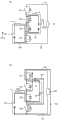
图1是表示本发明的实施方式的电源系统的结构例的电路图。FIG. 1 is a circuit diagram showing a configuration example of a power supply system according to an embodiment of the present invention.
参照图1,电源系统5具备直流电源10、直流电源20、负载30、控制装置40、电力转换器50。Referring to FIG. 1 , a
在本实施方式中,直流电源10及20由二次电池或双电荷层电容器等蓄电装置构成。例如,直流电源10由锂离子二次电池或镍氢电池那样的二次电池构成。而且,直流电源20例如由双电荷层电容器或锂离子电容器等的输出特性优异的直流电压源要素构成。直流电源10及直流电源20分别对应于“第一直流电源”及“第二直流电源”。但是,也可以通过同种的蓄电装置构成直流电源10及20。In the present embodiment, DC power supplies 10 and 20 are constituted by power storage devices such as secondary batteries and electric double layer capacitors. For example, the
电力转换器50连接在直流电源10及直流电源20和负载30之间。电力转换器50按照电压指令值来控制与负载30连接的电源配线PL上的直流电压(以下,也称为输出电压Vo)。
负载30接受电力转换器50的输出电压Vo而动作。输出电压Vo的电压指令值设定成与负载30的动作相适合的电压。电压指令值根据负载30的状态而可变地设定。此外,负载30也可以构成为,能够通过再生发电等而产生直流电源10、20的充电电力。The
电力转换器50包含电力用半导体开关元件S1~S4和电抗器L1、L2。在本实施方式中,作为电力用半导体开关元件(以下,也简称为“开关元件”),可以使用IGBT(Insulated Gate Bipolar Transistor)、电力用MOS(Metal Oxide Semiconductor)晶体管或电力用双极晶体管等。对于开关元件S1~S4,配置反向并联二极管D1~D4。开关元件S1~S4能够响应来自控制装置40的控制信号SG1~SG4来控制通断。The
开关元件S1电连接在电源配线PL和节点N1之间。电抗器L2连接在节点N1和直流电源20的正极端子之间。开关元件S2电连接在节点N1和N2之间。电抗器L1连接在节点N2和直流电源10的正极端子之间。开关元件S3电连接在节点N2和N3之间。开关元件S4电连接在节点N3和接地配线GL之间。接地配线GL与负载30及直流电源10的负极端子电连接。Switching element S1 is electrically connected between power supply line PL and node N1. Reactor L2 is connected between node N1 and the positive terminal of
控制装置40例如由具有未图示的CPU(Central Processing Unit)及存储器的电子控制单元(ECU)构成。控制装置40基于存储在存储器中的映射及程序,来进行使用了基于各传感器的检测值的运算处理。或者,控制装置40的至少一部分可以通过电子电路等硬件来执行规定的数值·逻辑运算处理。The
为了控制输出电压Vo,控制装置40生成对开关元件S1~S4的通断进行控制的控制信号SG1~SG4。In order to control the output voltage Vo, the
此外,在图1中虽然省略图示,但设有直流电源10的电压(标记为V[1])及电流(标记为I[1])、直流电源20的电压(标记为V[2])及电流(标记为I[2])、以及输出电压Vo的检测器(电压传感器、电流传感器)。这些检测器的输出向控制装置40提供。In addition, although not shown in FIG. 1 , the voltage (marked as V[1]) and current (marked as I[1]) of the
根据图1可知,电力转换器50成为分别对应于直流电源10及直流电源20而具备升压斩波电路的结构。即,相对于直流电源10,构成以开关元件S1、S2为上支路元件而以开关元件S3、S4为下支路元件的电流双向的第一升压斩波电路。同样地,相对于直流电源20,构成以开关元件S1、S4为上支路元件而以开关元件S2、S3为下支路元件的电流双向的第二升压斩波电路。并且,通过第一升压斩波电路而形成于直流电源10和电源配线PL之间的电力转换路径和通过第二升压斩波电路而形成于直流电源10和电源配线PL之间的电力转换路径双方包含开关元件S1~S4。As can be seen from FIG. 1 ,
此外,对于升压斩波电路中的电压转换比(升压比),已知使用低压侧(直流电源侧)的电压Vi、高压侧(负载侧)的电压VH及下支路元件的占空比DT,由下述(1)式表示。此外,占空比DT由下支路元件的接通期间与下支路元件的接通期间及断开期间之和即开关周期之比来定义。此外,在下支路元件的断开期间,上支路元件接通。In addition, for the voltage conversion ratio (boost ratio) in the step-up chopper circuit, it is known to use the voltage Vi of the low-voltage side (DC power supply side), the voltage VH of the high-voltage side (load side), and the duty of the lower arm element The ratio DT is represented by the following formula (1). In addition, the duty ratio DT is defined by the ratio of the ON period of the lower arm element to the sum of the ON period and the OFF period of the lower arm element, that is, the switching period. Furthermore, the upper branch element is switched on during the off period of the lower branch element.
VH=1/(1-DT)·Vi...(1)VH=1/(1-DT)·Vi...(1)
此外,在本实施方式的电力转换器50中,电力转换器50通过开关元件S1~S4的控制,能够切换并联连接模式与串联连接模式而动作,该并联连接模式是直流电源10、20并联连接的状态下在与负载30之间进行电力的交接的连接模式,该串联连接模式是串联连接的直流电源10、20在与负载30之间执行电力的交接的连接模式。并联连接模式对应于“第一动作模式”,串联连接模式对应于“第二动作模式”。在实施方式1中,说明并联连接模式下的控制动作,尤其是基于开关元件的电力损失减少用的控制。In addition, in the
(并联连接模式下的电路动作)(Circuit operation in parallel connection mode)
对电力转换器50的并联连接模式下的电路动作进行说明。The circuit operation in the parallel connection mode of the
如图2及图3所示,通过将开关元件S4或S2设为接通,能够将直流电源10及20相对于电源配线PL并联连接。在此,在并联连接模式下,根据直流电源10的电压V[1]和直流电源20的电压V[2]的高低,等价电路不同。As shown in FIGS. 2 and 3 , by turning on switching element S4 or S2 , DC power supplies 10 and 20 can be connected in parallel to power supply line PL. Here, in the parallel connection mode, the equivalent circuit differs depending on the voltage V[1] of the
如图2(a)所示,V[2]>V[1]时,通过将开关元件S4设为接通,经由开关元件S2、S3,将直流电源10及20并联连接。此时的等价电路如图2(b)所示。As shown in FIG. 2( a ), when V[2]>V[1], switching element S4 is turned on, and DC power supplies 10 and 20 are connected in parallel via switching elements S2 and S3 . The equivalent circuit at this time is shown in Figure 2(b).
参照图2(b),在直流电源10及电源配线PL之间,通过开关元件S3的通断控制,能够交替形成下支路元件的接通期间及断开期间。同样地,在直流电源20及电源配线PL之间,通过将开关元件S2、S3共同地进行通断控制,能够交替地形成升压斩波电路的下支路元件的接通期间及断开期间。此外,开关元件S1作为对来自负载30的再生进行控制的开关而动作。Referring to FIG. 2( b ), between the
另一方面,如图3(a)所示,在V[1]>V[2]时,通过将开关元件S2接通,经由开关元件S3、S4将直流电源10及20并联连接。此时的等价电路如图3(b)所示。On the other hand, as shown in FIG. 3( a ), when V[1]>V[2], switching element S2 is turned on, and DC power supplies 10 and 20 are connected in parallel via switching elements S3 and S4 . The equivalent circuit at this time is shown in Figure 3(b).
参照图3(b),在直流电源20及电源配线PL之间,通过开关元件S3的通断控制,能够交替地形成下支路元件的接通期间及断开期间。同样地,在直流电源10及电源配线PL之间,通过对开关元件S3、S4共同地进行通断控制,能够交替地形成升压斩波电路的下支路元件的接通期间及断开期间。此外,开关元件S1作为对来自负载30的再生进行控制的开关而动作。Referring to FIG. 3( b ), between the
在图3及图4所示的电路动作中,无论在何种情况下都需要蓄积于电抗器L1、L2的能量的放出路径。当流动有不同的电流的电抗器彼此经由开关元件而被串联连接时,蓄积能量与电流的关系产生矛盾,可能产生火花等而导致电路破坏。因此,在电路上必须设置用于将电抗器L1、L2的蓄积能量放出的回流路径。In the circuit operation shown in FIG. 3 and FIG. 4 , in any case, a discharge path for the energy accumulated in the reactors L1 and L2 is required. When reactors through which different currents flow are connected in series via switching elements, the relationship between stored energy and current is contradictory, sparks may be generated, and the circuit may be destroyed. Therefore, it is necessary to provide a return path for releasing the stored energy of the reactors L1 and L2 on the circuit.
图4示出图2所示的电路动作时(V[2]>V[1]的并联连接模式)的电抗器的回流路径。图4(a)示出与电抗器L1对应的回流路径,图4(b)示出对于电抗器L2的回流路径。FIG. 4 shows the return path of the reactor when the circuit shown in FIG. 2 operates (parallel connection mode of V[2]>V[1]). FIG. 4( a ) shows a return path corresponding to the reactor L1 , and FIG. 4( b ) shows a return path for the reactor L2 .
参照图4(a),在图2(b)的等价电路中,输出状态下的电抗器L1的电流能够通过经由二极管D2、D1、电源配线PL、负载30及接地配线GL的电流路径102而回流。而且,再生状态下的电抗器L1的电流能够通过经由二极管D3的电流路径103而回流。通过电流路径102、103能够将蓄积于电抗器L1的能量放出。Referring to Fig. 4(a), in the equivalent circuit of Fig. 2(b), the current of the reactor L1 in the output state can pass through the current through the diodes D2, D1, the power line PL, the
参照图4(b),在图2(b)的等价电路中,输出状态下的电抗器L2的电流能够通过经由二极管D1、电源配线PL、负载30及接地配线GL的电流路径104而回流。而且,再生状态下的电抗器L2的电流通能够过经由二极管D3、D2的电流路径105而回流。通过电流路径104、105,能够将蓄积于电抗器L2的能量放出。Referring to FIG. 4(b), in the equivalent circuit of FIG. 2(b), the current of the reactor L2 in the output state can pass through the
图5示出图3所示的电路动作时(V[1]>V[2]的并联连接模式)的电抗器的回流路径。图5(a)示出与电抗器L1对应的回流路径,图5(b)示出对于电抗器L2的回流路径。FIG. 5 shows the return path of the reactor when the circuit shown in FIG. 3 operates (parallel connection mode of V[1]>V[2]). FIG. 5( a ) shows a return path corresponding to the reactor L1 , and FIG. 5( b ) shows a return path for the reactor L2 .
参照图5(a),在图3(b)的等价电路中,输出状态下的电抗器L1的电流能够通过经由二极管D1、电源配线PL、负载30及接地配线GL的电流路径106而回流。而且,再生状态下的电抗器L1的电流能够通过经由二极管D4、D3的电流路径107而回流。通过电流路径106、107,能够将蓄积于电抗器L1的能量放出。Referring to FIG. 5(a), in the equivalent circuit of FIG. 3(b), the current of the reactor L1 in the output state can pass through the current path 106 via the diode D1, the power supply line PL, the
参照图5(b),在图3(b)的等价电路中,输出状态下的电抗器L2的电流能够通过经由二极管D1、电源配线PL、负载30、接地配线GL及二极管D4的电流路径108而回流。而且,再生状态下的电抗器L2的电流能够通过经由二极管D3的电流路径109而回流。通过电流路径108、109,能够将蓄积于电抗器L2的能量放出。5(b), in the equivalent circuit of FIG. 3(b), the current of the reactor L2 in the output state can pass through the diode D1, the power line PL, the
如以上那样,在电力转换器50中,在并联连接模式下的动作时,无论在何种动作状态下,都能够确保将蓄积于电抗器L1、L2的能量放出的回流路径。As described above, when the
接下来,使用图6及图7,详细说明电力转换器50的并联连接模式下的升压动作。Next, the step-up operation of
图6示出并联连接模式下的对直流电源10的直流电力转换(升压动作)。FIG. 6 shows the DC power conversion (boosting operation) to the
参照图6(a),将一对开关元件S3、S4接通,将一对开关元件S1、S2断开,由此形成用于向电抗器L1蓄积能量的电流路径120。由此,形成将升压斩波电路的下支路元件接通的状态。Referring to FIG. 6( a ), the pair of switching elements S3 and S4 are turned on and the pair of switching elements S1 and S2 are turned off to form a
相对于此,参照图6(b),将一对开关元件S3、S4断开,并将一对开关元件S1、S2接通,由此形成用于将电抗器L1的蓄积能量与直流电源10的能量一起输出的电流路径121。由此,形成将升压斩波电路的上支路元件接通的状态。On the other hand, referring to FIG. 6( b ), the pair of switching elements S3 and S4 are turned off, and the pair of switching elements S1 and S2 are turned on, thereby forming a circuit for connecting the stored energy of the reactor L1 to the
交替地反复进行一对开关元件S3、S4处于接通而开关元件S1、S2的至少一方处于断开的第一期间和一对开关元件S1、S2处于接通而开关元件S3、S4的至少一方处于断开的第二期间,由此交替地形成图6(a)的电流路径120及图6(b)的电流路径121。The first period in which the pair of switching elements S3 and S4 are turned on and at least one of the switching elements S1 and S2 is turned off and the pair of switching elements S1 and S2 are turned on and at least one of the switching elements S3 and S4 are alternately repeated. During the second off period, the
其结果是,将一对开关元件S1、S2等价地形成为上支路元件并将一对开关元件S3、S4等价地形成为下支路元件的升压斩波电路相对于直流电源10而构成。在图6所示的直流电力转换动作中,由于没有向直流电源20流通的电流流通路径,因此直流电源10及20彼此不干扰。即,能够独立地控制相对于直流电源10及20的电力的输入输出。As a result, a step-up chopper circuit in which a pair of switching elements S1 and S2 are equivalently formed as upper arm elements and a pair of switching elements S3 and S4 are equivalently formed as lower arm elements is configured for the
在这种直流电力转换中,在直流电源10的电压V[1]与电源配线PL的输出电压Vo之间,下述(2)式所示的关系成立。在(2)式中,设将一对开关元件S3、S4接通的第一期间的占空比为Da。In such a DC power conversion, the relationship shown in the following formula (2) holds between the voltage V[1] of the
Vo=1/(1-Da)·V[1]...(2)Vo=1/(1-Da)·V[1]...(2)
在图7中示出并联连接模式下的对直流电源20的直流电力转换(升压动作)。FIG. 7 shows the DC power conversion (boosting operation) to the
参照图7(a),将一对开关元件S2、S3接通,并将一对开关元件S1、S4断开,由此形成用于向电抗器L2蓄积能量的电流路径130。由此,形成将升压斩波电路的下支路元件接通的状态。Referring to FIG. 7( a ), the pair of switching elements S2 and S3 are turned on and the pair of switching elements S1 and S4 are turned off to form a
相对于此,参照图7(b),将一对开关元件S2、S3断开,并将一对开关元件S1、S4接通,由此形成用于将电抗器L2的蓄积能量与直流电源20的能量一起输出的电流路径131。由此,形成将升压斩波电路的上支路元件接通的状态。On the other hand, referring to FIG. 7( b ), a pair of switching elements S2 and S3 are turned off, and a pair of switching elements S1 and S4 are turned on, thereby forming a circuit for connecting the stored energy of the reactor L2 to the
交替地反复进行一对开关元件S2、S3处于接通而开关元件S1、S4的至少一方处于断开的第一期间和一对开关元件S1、S4处于接通而开关元件S2、S3的至少一方处于断开的第二期间,由此交替地形成图7(a)的电流路径130及图7(b)的电流路径131。The first period in which the pair of switching elements S2 and S3 are turned on and at least one of the switching elements S1 and S4 is turned off and the pair of switching elements S1 and S4 are turned on and at least one of the switching elements S2 and S3 are alternately repeated. During the second off period, the
其结果是,将一对开关元件S1、S4等价地设为上支路元件并将一对开关元件S2、S3等价地设为下支路元件的升压斩波电路相对于直流电源20构成。在图7所示的直流电力转换动作中,没有向直流电源10流通的电流流通路径,因此直流电源10及20彼此不干扰。即,能够独立地控制相对于直流电源10及20的电力的输入输出。As a result, the step-up chopper circuit in which the pair of switching elements S1 and S4 are equivalently used as upper arm elements and the pair of switching elements S2 and S3 are equivalently used as lower arm elements is relatively stable compared to the
在这种直流电力转换中,在直流电源20的电压V[2]与电源配线PL的输出电压Vo之间,下述(3)式所示的关系成立。在(3)式中,设将一对开关元件S2、S3接通的第一期间的占空比为Db。In such a DC power conversion, the relationship shown in the following formula (3) holds between the voltage V[2] of the
Vo=1/(1-Db)·V[2]...(3)Vo=1/(1-Db)·V[2]...(3)
(并联连接模式下的基本的控制动作)(Basic control action in parallel connection mode)
说明电力转换器50的并联连接模式下的控制动作。以下说明的控制动作通过基于控制装置40的硬件处理和/或软件处理而实现。The control operation in the parallel connection mode of
图8示出并联连接模式下的从负载侧观察到的等价电路。FIG. 8 shows an equivalent circuit seen from the load side in a parallel connection mode.
参照图8,在并联连接模式下,在直流电源10与负载30之间执行直流电力转换的电源PS1和在直流电源20与负载30之间执行直流电力转换的电源PS2并列地对负载30交接电力。电源PS1相当于图6所示的执行直流电力转换动作的升压斩波电路。同样地,电源PS2相当于图7所示的执行直流电力转换动作的升压斩波电路。8, in the parallel connection mode, the power supply PS1 performing DC power conversion between the
即,电源PS1在直流电源10的电压V[1]和输出电压Vo之间具有基于式(2)所示的电压转换比的直流电力转换功能。同样地,电源PS2在直流电源20的电压V[2]及输出电压Vo之间具有基于式(3)所示的电压转换比的直流电力转换功能。That is, the power supply PS1 has a DC power conversion function based on the voltage conversion ratio shown in Formula (2) between the voltage V[1] of the
在并联连接模式下,若在双方的电源中同时执行共同的控制(输出电压Vo的电压控制),则在负载侧,成为将电源PS1及PS2并联连接的方式,因此电路可能损坏。因此,电源PS1及电源PS2中的一方的电源作为控制输出电压Vo的电压源而进行动作。并且,电源PS1及电源PS2中的另一方的电源作为将该电源的电流控制成电流指令值的电流源而进行动作。各电源PS1、PS2的电压转换比被控制成作为电压源或电流源进行动作。In the parallel connection mode, if the common control (voltage control of the output voltage Vo) is executed simultaneously on both power supplies, the power supplies PS1 and PS2 will be connected in parallel on the load side, and thus the circuit may be damaged. Therefore, one of the power supply PS1 and the power supply PS2 operates as a voltage source that controls the output voltage Vo. Then, the other power supply of the power supply PS1 and the power supply PS2 operates as a current source that controls the current of the power supply to a current command value. The voltage conversion ratio of each power supply PS1, PS2 is controlled so as to operate as a voltage source or a current source.
在将电源PS1设为电流源并将电源PS2设为电压源而进行控制的情况下,在直流电源10的电力P[1]、直流电源20的电力P[2]、负载30的电力Po及电流源中的电流指令值Ii*之间,下述(4)式的关系成立。In the case of controlling the power supply PS1 as a current source and the power supply PS2 as a voltage source, the power P[1] of the
P[2]=Po-P[1]=Po-V[1]·Ii*...(4)P[2]=Po-P[1]=Po-V[1]·Ii*...(4)
根据直流电源10的电压V[1]的检测值,若以P*=V[1]·Ii*成为恒定的方式设定电流指令值Ii*,则能够将构成电流源的直流电源10的电力P[1]控制成电力指令值Pi*。Based on the detected value of the voltage V[1] of the
相对于此,在将电源PS2设为电流源并将电源PS1设为电压源而进行控制的情况下,下述(5)式的关系成立。On the other hand, when the power supply PS2 is used as a current source and the power supply PS1 is controlled as a voltage source, the relationship of the following (5) formula holds.
P[1]=Po-P[2]=Po-V[2]·Ii*...(5)P[1]=Po-P[2]=Po-V[2]·Ii*...(5)
同样地,关于构成电流源的直流电源20的电力P[2],也是若以P*=V[2]·Ii*成为恒定的方式设定电流指令值Ii*,则能够控制成电力指令值Pi*。Similarly, for the power P[2] of the
图9示出用于说明与直流电源10对应的电源PS1的具体的控制动作例的波形图。FIG. 9 shows a waveform diagram for explaining a specific control operation example of the power supply PS1 corresponding to the
参照图9,电源PS1的占空比Da(参照式(2))通过作为电压源而进行动作用的电压反馈控制(图11)或作为电流源进行动作用的电流反馈控制(图12)来算出。此外,在图9中,表示占空比Da的电压信号由相同附图标记Da表示。Referring to Fig. 9, the duty ratio Da of the power supply PS1 (refer to formula (2)) is determined by voltage feedback control (Fig. 11) for operating as a voltage source or current feedback control (Fig. 12) for operating as a current source. figured out. Furthermore, in FIG. 9 , the voltage signal representing the duty ratio Da is denoted by the same reference symbol Da.
电源PS1的控制脉冲信号SDa通过基于占空比Da与周期性的载波信号25的比较而进行的脉宽调制(PWM)控制来生成。一般而言,载波信号25使用三角波或锯齿形波。载波信号25的周期相当于各开关元件的开关频率,载波信号25的振幅设定为与Da=1.0对应的电压。The control pulse signal SDa of the power supply PS1 is generated by pulse width modulation (PWM) control based on a comparison between the duty ratio Da and the
在表示占空比Da的电压比载波信号25的电压高时,控制脉冲信号SDa被设定为逻辑高电平(以下,称为H电平),而在比载波信号25的电压低时,控制脉冲信号SDa被设定为逻辑低电平(以下,称为L电平)。H电平期间与控制脉冲信号SDa的周期(H电平期间+L电平期间)之比即控制脉冲信号SDa的占空比与Da相等。When the voltage representing the duty ratio Da is higher than the voltage of the
控制脉冲信号/SDa是控制脉冲信号SDa的反转信号。当占空比Da升高时,控制脉冲信号SDa的H电平期间变长。相反地,当占空比Da降低时,控制脉冲信号SDa的L电平期间变长。The control pulse signal /SDa is an inverted signal of the control pulse signal SDa. As the duty ratio Da increases, the H level period of the control pulse signal SDa becomes longer. Conversely, when the duty ratio Da decreases, the L level period of the control pulse signal SDa becomes longer.
控制脉冲信号SDa对应于对图6所示的升压斩波电路的下支路元件的通断进行控制的信号。即,在控制脉冲信号SDa的H电平期间,下支路元件接通,而在L电平期间,下支路元件断开。另一方面,控制脉冲信号/SDa对应于对图6所示的升压斩波电路的上支路元件的通断进行控制的信号。The control pulse signal SDa corresponds to a signal for controlling the switching on and off of the lower arm element of the step-up chopper circuit shown in FIG. 6 . That is, during the H level period of the control pulse signal SDa, the lower arm element is turned on, and during the L level period, the lower arm element is turned off. On the other hand, the control pulse signal /SDa corresponds to a signal for controlling ON/OFF of the upper arm element of the step-up chopper circuit shown in FIG. 6 .
图10示出用于说明与直流电源20对应的电源PS2的具体的控制动作例的波形图。FIG. 10 is a waveform diagram illustrating a specific control operation example of the power supply PS2 corresponding to the
参照图10,在电源PS2中,也通过与电源PS1同样的PWM控制,并基于占空比Db(参照式(3))来生成控制脉冲信号SDb及其反转信号/SDb。控制脉冲信号SDb的占空比与Db相等,控制脉冲信号/SDb的占空比与(1.0-Db)相等。即,当占空比Db升高时,控制脉冲信号SDb的H电平期间变长。相反地,当占空比Db降低时,控制脉冲信号SDb的L电平期间变长。Referring to FIG. 10 , also in power supply PS2 , control pulse signal SDb and its inverted signal /SDb are generated based on duty ratio Db (refer to equation (3)) by the same PWM control as power supply PS1 . The duty ratio of the control pulse signal SDb is equal to Db, and the duty ratio of the control pulse signal /SDb is equal to (1.0-Db). That is, as the duty ratio Db increases, the H level period of the control pulse signal SDb becomes longer. Conversely, when the duty ratio Db decreases, the L level period of the control pulse signal SDb becomes longer.
控制脉冲信号SDb对应于对图7所示的升压斩波电路的下支路元件的通断进行控制的信号。控制脉冲信号/SDb对应于对图7所示的升压斩波电路的上支路元件的通断进行控制的信号。The control pulse signal SDb corresponds to a signal for controlling the switching on and off of the lower arm element of the step-up chopper circuit shown in FIG. 7 . The control pulse signal /SDb corresponds to a signal for controlling the switching on and off of the upper arm element of the step-up chopper circuit shown in FIG. 7 .
此外,在电源PS1作为电压源进行动作时,占空比Db通过电源PS2作为电流源进行动作用的电流反馈控制(图12)来算出。相反地,在电源PS1作为电流源进行动作时,占空比Db通过电源PS2作为电压源而进行动作用的电压反馈控制(图11)来算出。In addition, when the power supply PS1 operates as a voltage source, the duty ratio Db is calculated by current feedback control ( FIG. 12 ) for the power supply PS2 to operate as a current source. Conversely, when the power supply PS1 operates as a current source, the duty ratio Db is calculated by voltage feedback control ( FIG. 11 ) for the power supply PS2 to operate as a voltage source.
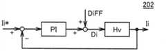
图11示出作为电压源进行动作的电源的控制块201的结构例。FIG. 11 shows a configuration example of a
参照图11,控制块201根据反馈控制量与前馈控制量DvFF之和来生成电压控制用的占空比指令值Dv,其中该反馈控制量是对输出电压Vo的电压指令值Vo*与输出电压Vo(检测值)的偏差进行了PI(比例积分)运算而得到的。传递函数Hv相当于作为电压源而动作的电源PS1或PS2的传递函数。Referring to Fig. 11, the
图12示出作为电流源而动作的电源的控制块202的结构例。FIG. 12 shows a configuration example of a
参照图12,控制块202根据反馈控制量与前馈控制量DiFF之和来生成电流控制用的占空比指令值Di,其中该反馈控制量是对电流指令值Ii*与电流控制的直流电源10或20的电流Ii(检测值)的偏差进行了PI(比例积分)运算而得到的。传递函数Hi相当于作为电流源进行动作的电源PS2或PS1的传递函数。Referring to Fig. 12, the
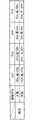
图13示出并联连接模式下的各控制数据的设定。在图13的左栏中,示出将电源PS1(直流电源10)设为电流源并将电源PS2(直流电源20)设为电压源而进行控制的情况下的各控制数据的设定。Fig. 13 shows the setting of each control data in the parallel connection mode. In the left column of FIG. 13 , settings of each control data are shown when the power supply PS1 (DC power supply 10 ) is used as a current source and the power supply PS2 (DC power supply 20 ) is controlled as a voltage source.
参照图13的左栏,电压控制用的占空比指令值Dv使用电源PS2(直流电源20)的占空比Db,并且电流控制用的占空比指令值Di使用电源PS1(直流电源10)的占空比Da。通过电流控制而控制的电流Ii成为直流电源10的电流I[1]。此外,无论以电源PS1、PS2的哪一个为电压源,通过电压控制而控制的电压都为输出电压Vo。Referring to the left column of FIG. 13 , the duty ratio command value Dv for voltage control uses the duty ratio Db of the power supply PS2 (DC power supply 20 ), and the duty ratio command value Di for current control uses the power supply PS1 (DC power supply 10 ). The duty cycle is Da. The current Ii controlled by the current control becomes the current I[1] of the
图11中的传递函数Hv相当于与图7所示的直流电源20对应的升压斩波电路的传递函数。而且,图12中的传递函数Hi相当于与图6所示的直流电源10对应的升压斩波电路的传递函数。The transfer function Hv in FIG. 11 corresponds to the transfer function of the step-up chopper circuit corresponding to the
如下述(6)式所示,电压控制中的前馈控制量DvFF根据输出电压Vo与直流电源20的电压V[2]的电压差而设定。而且,如下述(7)式所示,电流控制中的前馈控制量DiFF根据输出电压Vo与直流电源10的电压V[1]的电压差而设定。The feedforward control amount DvFF in the voltage control is set according to the voltage difference between the output voltage Vo and the voltage V[ 2 ] of the
DvFF=(Vo-V[2])/Vo...(6)DvFF=(Vo-V[2])/Vo...(6)
DiFF=(Vo-V[1])/Vo...(7)DiFF=(Vo-V[1])/Vo...(7)
根据占空比Da(Da=Di),生成图9所示的控制脉冲信号SDa及/SDa。同样地,根据占空比Db(Db=Dv),生成图10所示的控制脉冲信号SDb及/SDb。According to the duty ratio Da (Da=Di), control pulse signals SDa and /SDa shown in FIG. 9 are generated. Similarly, the control pulse signals SDb and /SDb shown in FIG. 10 are generated according to the duty ratio Db (Db=Dv).
用于分别对开关元件S1~S4的通断进行控制的控制信号SG1~SG4基于电源PS1的电流控制用的控制脉冲信号和电源PS2的电压控制用的控制信号脉冲而设定。具体而言,控制信号SG1~SG4基于控制脉冲信号间的逻辑运算(更确切而言,以取得逻辑和的方式)而设定。Control signals SG1 to SG4 for respectively controlling on and off of switching elements S1 to S4 are set based on a control pulse signal for current control of power supply PS1 and a control signal pulse for voltage control of power supply PS2 . Specifically, the control signals SG1 to SG4 are set based on a logical operation (more precisely, a logical sum) between the control pulse signals.
开关元件S1在图6及图7的升压斩波电路上分别形成上支路元件。因此,对开关元件S1的通断进行控制的控制信号SG1通过控制脉冲信号/SDa与/SDb的逻辑和而生成。即,控制信号SG1将控制脉冲信号/SDa与/SDb的至少一方在H电平的期间被设定为H电平。并且,控制信号SG1将控制脉冲信号/SDa与/SDb双方在L电平的期间被设定为L电平。The switching element S1 forms an upper arm element in the step-up chopper circuits of FIGS. 6 and 7 . Therefore, the control signal SG1 for controlling the switching element S1 is generated by the logical sum of the control pulse signals /SDa and /SDb. That is, the control signal SG1 sets at least one of the control pulse signals /SDa and /SDb to the H level while the control signal SG1 is at the H level. In addition, the control signal SG1 sets both the control pulse signals /SDa and /SDb to the L level while they are at the L level.
其结果是,对开关元件S1进行通断控制,以实现图6的升压斩波电路(直流电源10)的上支路元件及图7的升压斩波电路(直流电源20)的上支路元件双方的功能。As a result, the switching element S1 is controlled on and off to realize the upper branch element of the boost chopper circuit (DC power supply 10) in FIG. 6 and the upper branch circuit component of the boost chopper circuit (DC power supply 20) in FIG. function of both sides of the circuit element.
开关元件S2在图6的升压斩波电路中形成上支路元件,在图7的升压斩波电路中形成下支路元件。因此,对开关元件S2的通断进行控制的控制信号SG2通过控制脉冲信号/SDa与SDb的逻辑和而生成。即,控制信号SG2将控制脉冲信号/SDa与SDb的至少一方在H电平的期间被设定成H电平。并且,控制信号SG2将控制脉冲信号/SDa与SDb双方在L电平的期间被设定为L电平。由此,对开关元件S2进行通断控制,以实现图6的升压斩波电路(直流电源10)的上支路元件及图7的升压斩波电路(直流电源20)的下支路元件双方的功能。Switching element S2 forms an upper arm element in the boost chopper circuit of FIG. 6 and a lower arm element in the boost chopper circuit of FIG. 7 . Therefore, the control signal SG2 for controlling the switching element S2 is generated by the logical sum of the control pulse signals /SDa and SDb. That is, the control signal SG2 sets at least one of the control pulse signals /SDa and SDb to be at the H level while at least one of the control pulse signals /SDa and SDb is at the H level. In addition, the control signal SG2 sets both the control pulse signals /SDa and SDb to the L level while they are at the L level. Thus, on-off control is performed on the switching element S2 to realize the upper branch circuit element of the boost chopper circuit (DC power supply 10) in FIG. 6 and the lower branch circuit of the boost chopper circuit (DC power supply 20) in FIG. 7 The function of both sides of the component.
同样地,开关元件S3的控制信号SG3通过控制脉冲信号SDa与SDb的逻辑和而生成。由此,对开关元件S3进行通断控制,以实现图6的升压斩波电路(直流电源10)的下支路元件及图7的升压斩波电路(直流电源20)的下支路元件双方的功能。Similarly, the control signal SG3 of the switching element S3 is generated by the logical sum of the control pulse signals SDa and SDb. Thus, on-off control is performed on the switching element S3 to realize the lower branch circuit element of the step-up chopper circuit (DC power supply 10) in FIG. 6 and the lower branch circuit of the step-up chopper circuit (DC power supply 20) in FIG. 7 The function of both sides of the component.
另外,开关元件S4的控制信号SG4通过控制脉冲信号SDa与/SDb的逻辑和而生成。由此,对开关元件S4进行通断控制,以实现图6的升压斩波电路(直流电源10)的下支路元件及图7的升压斩波电路(直流电源20)的上支路元件双方的功能。In addition, the control signal SG4 of the switching element S4 is generated by the logical sum of the control pulse signals SDa and /SDb. Thus, on-off control is performed on the switching element S4 to realize the lower branch circuit element of the step-up chopper circuit (DC power supply 10 ) in FIG. 6 and the upper branch circuit of the step-up chopper circuit (DC power supply 20 ) in FIG. 7 The function of both sides of the component.
在图13的右栏,示出将电源PS1(直流电源10)设为电压源并将电源PS2(直流电源20)设为电流源而控制的情况下的各控制数据的设定。The right column of FIG. 13 shows the setting of each control data when controlling the power supply PS1 (DC power supply 10 ) as a voltage source and controlling the power supply PS2 (DC power supply 20 ) as a current source.
参照图13的右栏,电压控制用的占空比指令值Dv使用电源PS1(直流电源10)的占空比Da,并且电流控制用的占空比指令值Di使用电源PS2(直流电源20)的占空比Db。通过电流控制而控制的电流Ii成为直流电源20的电流I[2]。通过电压控制而控制的电压为输出电压Vo。Referring to the right column of FIG. 13 , the duty ratio command value Dv for voltage control uses the duty ratio Da of the power supply PS1 (DC power supply 10 ), and the duty ratio command value Di for current control uses the power supply PS2 (DC power supply 20 ). The duty cycle Db. The current Ii controlled by the current control becomes the current I[2] of the
图11中的传递函数Hv相当于与图6所示的直流电源10对应的升压斩波电路的传递函数。而且,图12中的传递函数Hi相当于与图7所示的直流电源20对应的升压斩波电路的传递函数。The transfer function Hv in FIG. 11 corresponds to the transfer function of the step-up chopper circuit corresponding to the
如下述(8)式所示,电压控制中的前馈控制量DvFF根据输出电压Vo与直流电源20的电压V[1]的电压差而设定。而且,如下述(9)式所示,电流控制中的前馈控制量DiFF根据输出电压Vo与直流电源10的电压V[2]的电压差而设定。The feedforward control amount DvFF in the voltage control is set according to the voltage difference between the output voltage Vo and the voltage V[ 1 ] of the
DvFF=(Vo-V[1])/Vo...(8)DvFF=(Vo-V[1])/Vo...(8)
DiFF=(Vo-V[2])/Vo...(9)DiFF=(Vo-V[2])/Vo...(9)
根据占空比Da(Da=Dv),生成图9所示的控制脉冲信号SDa及/SDa。同样地,根据占空比Db(Db=Di),生成图10所示的控制脉冲信号SDb及/SDb。Control pulse signals SDa and /SDa shown in FIG. 9 are generated according to the duty ratio Da (Da=Dv). Similarly, the control pulse signals SDb and /SDb shown in FIG. 10 are generated according to the duty ratio Db (Db=Di).
用于分别对开关元件S1~S4的通断进行控制的控制信号SG1~SG4以取得电源PS1的电压控制用的控制脉冲信号与电源PS2的电流控制用的控制信号脉冲的逻辑和的的方式而设定。即,无论直流电源10及直流电源20中的电压控制及电流控制的组合如何,开关元件S1~S4的控制信号SG1~SG4均同样地生成。The control signals SG1 to SG4 for controlling the on and off of the switching elements S1 to S4 are obtained by taking the logical sum of the control pulse signal for voltage control of the power supply PS1 and the control signal pulse for current control of the power supply PS2. set up. That is, regardless of the combination of voltage control and current control in
在并联连接模式下,控制信号SG2及SG4设定为互补的电平,因此开关元件S2及S4互补地进行接通断开。由此,图2所示的V[2]>V[1]时的动作与图3所示的V[1]>V[2]的动作被自然地切换。而且,在各动作中,通过使开关元件S1、S3互补地接通断开,分别在电源PS1、PS2中,能够执行按照占空比Da、Db的直流电力转换。In the parallel connection mode, since the control signals SG2 and SG4 are set to complementary levels, the switching elements S2 and S4 are turned on and off in a complementary manner. Thereby, the operation when V[2]>V[1] shown in FIG. 2 and the operation when V[1]>V[2] shown in FIG. 3 are naturally switched. Furthermore, in each operation, switching elements S1 and S3 are turned on and off in a complementary manner, so that DC power conversion according to duty ratios Da and Db can be performed in power supplies PS1 and PS2 , respectively.
(并联连接模式下的开关损失减少用的控制动作)(Control action for reducing switching loss in parallel connection mode)
如上所述,在使本发明的实施方式的电力转换器50以并联连接模式进行动作的情况下,并列地对直流电源10及直流电源20的各个直流电源执行PWM控制。在此,对在直流电源10及直流电源20的PWM控制中所使用的载波信号的相位进行说明。As described above, when
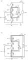
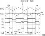
在图14中,示出使用了相同相位的载波信号的情况下的并联连接模式的控制动作例。另一方面,图15是表示使用了相位不同的载波信号的情况下的并联连接模式的控制动作例的波形图。FIG. 14 shows an example of a control operation in the parallel connection mode when carrier signals of the same phase are used. On the other hand, FIG. 15 is a waveform diagram showing an example of a control operation in the parallel connection mode when carrier signals with different phases are used.
参照图14,在直流电源10的PWM控制中使用的载波信号25a与在直流电源20的PWM控制中使用的载波信号25b为相同频率且相同相位。Referring to FIG. 14 ,
基于占空比Da与载波信号25a的电压比较来生成控制脉冲信号SDa,该占空比Da是基于直流电源10的电压或电流而算出的。同样地,基于占空比Db与载波信号25b的比较来求出控制脉冲信号SDb,该占空比Db是基于直流电源20的电流或电压而算出的。控制脉冲信号/SDa、/SDb是控制脉冲信号SDa、SDb的反转信号。The control pulse signal SDa is generated based on a duty ratio Da calculated based on the voltage or current of the
控制信号SG1~SG4按照图13所示的逻辑运算,基于控制脉冲信号SDa(/SDa)及SDb(/SDb)的逻辑运算而设定。基于控制信号SG1~SG4对开关元件S1~S4进行接通断开,由此将在电抗器L1中流动的电流I(L1)及在电抗器L2中流动的电流I(L2)如图14所示地控制。电流I(L1)相当于直流电源10的电流I[1],电流I(L2)相当于直流电源20的电流I[2]。The control signals SG1 to SG4 are set based on the logical operation of the control pulse signals SDa (/SDa) and SDb (/SDb) according to the logical operation shown in FIG. 13 . The switching elements S1 to S4 are turned on and off based on the control signals SG1 to SG4, whereby the current I(L1) flowing in the reactor L1 and the current I(L2) flowing in the reactor L2 are shown in FIG. 14 display control. The current I ( L1 ) corresponds to the current I[ 1 ] of the
相对于此,在图15中,载波信号25a及载波信号25b为相同频率,但相位不同。在图15的例子中,载波信号25a及载波信号25b的相位差φ=180度。On the other hand, in FIG. 15, the
并且,与图14同样地,基于载波信号25a及占空比Da的比较来生成控制脉冲信号SDa,并基于载波信号25b及占空比Db的比较来生成控制脉冲信号SDb。14, the control pulse signal SDa is generated based on the comparison of the
在图15中,占空比Da、Db与图14为相同值。因此,图15的控制脉冲信号SDa与图14的控制脉冲信号SDa相比,虽然相位不同,但H电平期间的长度相同。同样地,图15的控制脉冲信号SDb与图14的控制脉冲信号SDb相比,虽然相位不同,但H电平期间的长度相同。In FIG. 15 , duty ratios Da and Db are the same values as in FIG. 14 . Therefore, the control pulse signal SDa of FIG. 15 is different from the control pulse signal SDa of FIG. 14 , but the length of the H level period is the same although the phase is different. Similarly, the control pulse signal SDb in FIG. 15 is different in phase from the control pulse signal SDb in FIG. 14 , but the length of the H level period is the same.
因此,通过在载波信号间设置相位差φ,图15的控制信号SG1~SG4成为与图14的控制信号SG1~SG4不同的波形。根据图14及图15的比较可知,通过改变载波信号25a、25b之间的相位差φ而使电流I(L1)及电流I(L2)的相位关系(电流相位)发生变化。Therefore, by providing the phase difference φ between the carrier signals, the control signals SG1 to SG4 in FIG. 15 have different waveforms from the control signals SG1 to SG4 in FIG. 14 . 14 and 15, it can be seen that by changing the phase difference φ between the carrier signals 25a and 25b, the phase relationship (current phase) between the current I(L1) and the current I(L2) changes.
另一方面,对于相同占空比Da、Db,可知电流I(L1)、I(L2)的平均值在图14及图15之间相等。即,直流电源10、20的输出由占空比Da、Db控制,即使改变载波信号25a、25b的相位差φ,也不会产生影响。On the other hand, for the same duty ratios Da and Db, it can be seen that the average values of the currents I( L1 ), I( L2 ) are equal between FIG. 14 and FIG. 15 . That is, the outputs of the DC power supplies 10 and 20 are controlled by the duty ratios Da and Db, and even if the phase difference φ of the carrier signals 25a and 25b is changed, there is no influence.
因此,在本发明的实施方式的电力转换器50中,在并联连接模式下,通过对载波信号25a及25b之间的相位差φ适当地进行调整的载波相位控制,来减少开关元件S1~S4的开关损失。Therefore, in the
以下,作为代表的例子,说明直流电源10及20双方为输出状态,即电流I(L1)>0且电流I(L2)>0的状态下的控制。Hereinafter, as a representative example, control in which both DC power supplies 10 and 20 are in the output state, that is, the state in which the current I( L1 )>0 and the current I( L2 )>0, will be described.
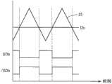
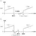
图16是对在电力转换器50中用于减少并联连接模式下的开关损失的、基于实施方式1的相位控制的电流相位进行说明的波形图。16 is a waveform diagram illustrating a current phase by phase control in the first embodiment for reducing switching loss in the parallel connection mode in the
参照图16,在时刻Ta之前,开关元件S2~S4接通,因此相对于直流电源10、20双方,升压斩波电路的下支路元件成为被接通的状态,因此,电流I(L1)及I(L2)双方上升。Referring to FIG. 16 , before the time Ta, the switching elements S2 to S4 are turned on, so the lower arm elements of the step-up chopper circuit are turned on with respect to both the DC power supplies 10 and 20, so the current I (L1 ) and I (L2) both rise.
在时刻Ta,开关元件S2被断开,由此,相对于直流电源20,升压斩波电路的下支路元件成为被断开的状态,因此电流I(L2)开始下降。与开关元件S2的断开相替换地,开关元件S1被接通。At time Ta, the switching element S2 is turned off, whereby the lower arm element of the step-up chopper circuit is turned off with respect to the
在时刻Ta以后,成为如下状态:相对于直流电源10,升压斩波电路的下支路元件被接通,相对于直流电源20,升压斩波电路的下支路元件被断开。即,电流I(L2)下降,而电流I(L1)上升。此时,电力转换器50的电流路径成为图17(a)那样。After time Ta, the lower arm element of the step-up chopper circuit is turned on with respect to the
根据图17(a)可知,在时刻Ta以后,电流I(L1)及I(L2)的差电流流过开关元件S4。即,开关元件S4的流过电流减小。It can be seen from FIG. 17( a ) that after the time Ta, a difference current between the currents I( L1 ) and I( L2 ) flows through the switching element S4 . That is, the current flowing through the switching element S4 decreases.
再次参照图16,从时刻Ta以后的状态开始,当开关元件S4被断开时,相对于直流电源10,升压斩波电路的下支路元件成为被断开的状态,因此电流I(L1)开始下降。而且,当开关元件S2被接通时,相对于直流电源20,升压斩波电路的下支路元件成为被接通的状态,因此电流I(L2)再次开始上升。即,电力转换器50中的电流路径从图17(a)的状态变化为图17(b)的状态。在图17(b)的状态下,电流I(L1)及I(L2)的差电流流过开关元件S2,因此开关元件S2的流过电流减小。Referring to FIG. 16 again, starting from the state after time Ta, when the switching element S4 is turned off, the lower arm element of the step-up chopper circuit is turned off with respect to the
在图17(a)的状态下将开关元件S4断开,由此能够减少开关元件S4的断开时的电流即开关损失。而且,在图17(b)的状态下将开关元件S2接通,由此能够减少开关元件S2的接通时的电流即开关损失。By turning off the switching element S4 in the state shown in FIG. 17( a ), it is possible to reduce the switching loss, which is the current when the switching element S4 is turned off. Furthermore, by turning on the switching element S2 in the state shown in FIG. 17( b ), it is possible to reduce the switching loss, which is the current when the switching element S2 is turned on.
因此,在实施方式1中,电流I(L1)的下降开始定时(即,极大点。以下,也简称为下降定时)与电流I(L2)的上升开始定时(即,极小点。以下,也简称为上升定时)重叠的方式,调整电流相位即载波信号25a、25b的相位差φ。由此,在图16的时刻Tb,将开关元件S2接通并将开关元件S4断开。Therefore, in
再次参照图16,在时刻Tc,将开关元件S1断开,并将开关元件S4接通。由此,分别相对于直流电源10、20,升压斩波电路的下支路元件都成为被接通的状态。由此,上述的时刻Ta以前的状态再现,电流I(L1)及I(L2)双方都上升。Referring again to FIG. 16 , at time Tc, the switching element S1 is turned off, and the switching element S4 is turned on. As a result, the lower arm elements of the step-up chopper circuit are all turned on with respect to the DC power supplies 10 and 20 , respectively. As a result, the state before the above-mentioned time Ta is reproduced, and both the currents I( L1 ) and I( L2 ) rise.
在图18中,示出图16所示的电流相位的开关元件S2、S4的电流波形。在图18(a)中,示出开关元件S2的电流I(S2)的波形,在图18(b)中,示出开关元件S4的电流I(S4)的波形。In FIG. 18 , current waveforms of switching elements S2 and S4 in the current phase shown in FIG. 16 are shown. In FIG. 18( a ), the waveform of the current I( S2 ) of the switching element S2 is shown, and in FIG. 18( b ), the waveform of the current I( S4 ) of the switching element S4 is shown.
参照图18(a),电流I(S2)在时刻Ta之前的期间及时刻Tc以后的期间,成为I(S2)=I(L2)。在时刻Ta~Tb的期间,开关元件S2断开,因此I(S2)=0。并且,在时刻Tb~Tc的期间,如图17(b)所示,成为I(S2)=-(I(L1)-I(L2))。Referring to FIG. 18( a ), the current I( S2 ) becomes I( S2 )=I( L2 ) in the period before time Ta and in the period after time Tc. During the period from time Ta to Tb, the switching element S2 is turned off, so I( S2 )=0. And, during the period from time Tb to Tc, as shown in FIG. 17( b ), I( S2 )=−(I( L1 )−I( L2 )).
参照图18(b),电流I(S4)在时刻Ta之前的期间及时刻Tc以后的期间,成为I(S4)=I(L1)。在时刻Ta~Tb的期间,如图17(a)所示,成为I(S4)=-(I(L2)-I(L1))。并且,在时刻Tb~Tc的期间,由于开关元件S4被断开,因此I(S4)=0。Referring to FIG. 18( b ), the current I( S4 ) becomes I( S4 )=I( L1 ) in the period before time Ta and in the period after time Tc. During the period from time Ta to Tb, as shown in FIG. 17( a ), I( S4 )=−(I( L2 )−I( L1 )). In addition, during the period from time Tb to Tc, since the switching element S4 is turned off, I( S4 )=0.
在图19中,示出用于与图16比较的、与图16同等的占空比下而载波信号间的相位差φ=0时的电流相位。In FIG. 19 , for comparison with FIG. 16 , current phases when the phase difference φ=0 between carrier signals at the same duty ratio as in FIG. 16 are shown.
参照图19,载波信号25a、25b的相位差φ=0时,电流I(L1)、I(L2)上升/下降的定时(Tx、Ty、Tz、Tw)互不相同。Referring to FIG. 19 , when the phase difference φ=0 of the carrier signals 25 a , 25 b , the rising/falling timings (Tx, Ty, Tz, Tw) of the currents I( L1 ), I( L2 ) are different from each other.
具体而言,在时刻Tx以前的开关元件S1处于断开且开关元件S2~S4处于接通的状态下,电流I(L1)及I(L2)双方都上升。并且,在时刻Tx,开关元件S4断开,由此电流I(L1)开始下降。与开关元件S4的断开相替换地,开关元件S1被接通。Specifically, when the switching element S1 is off and the switching elements S2 to S4 are on before the time Tx, both the currents I( L1 ) and I( L2 ) increase. Then, at time Tx, the switching element S4 is turned off, whereby the current I( L1 ) starts to drop. As an alternative to switching off switching element S4, switching element S1 is switched on.
并且,在时刻Ty,在时刻Tx,开关元件S3断开,由此电流I(L2)开始下降。与开关元件S3的断开相替换地,开关元件S4被接通。由此,电流I(L1)及I(L2)双方都下降。Then, at time Ty, at time Tx, the switching element S3 is turned off, whereby the current I( L2 ) starts to drop. As an alternative to switching off the switching element S3, the switching element S4 is switched on. Accordingly, both the currents I( L1 ) and I( L2 ) decrease.
在时刻Tz,将开关元件S2断开,并将开关元件S3接通。由此,相对于直流电源10,升压斩波电路的下支路元件成为接通的状态,因此电流I(L1)再次上升。而且,在时刻Tw,开关元件S1断开,并且开关元件S2接通。由此,再次出现时刻Tx以前的状态,因此电流I(L1)及I(L2)双方都上升。At time Tz, switching element S2 is turned off and switching element S3 is turned on. As a result, the lower arm element of the step-up chopper circuit is turned on with respect to the
在图20中,示出图19所示的电流相位下的开关元件S2、S4的电流波形。在图20(a)中,示出开关元件S2的电流I(S2)的波形,在图20(b)中,示出开关元件S4的电流I(S4)的波形。In FIG. 20 , current waveforms of switching elements S2 and S4 in the current phase shown in FIG. 19 are shown. In FIG. 20( a ), the waveform of the current I( S2 ) of the switching element S2 is shown, and in FIG. 20( b ), the waveform of the current I( S4 ) of the switching element S4 is shown.
参照图20(a),电流I(S2)在时刻Tx之前的期间及时刻Tw以后的期间,成为I(S2)=I(L2)。在时刻Tx~Ty的期间,形成与图17(b)同样的电流路径,因此成为I(S2)=-(I(L1)-I(L2))。并且,在时刻Ty~Tz的期间,作为相对于直流电源10的上支路元件进行动作,因此成为I(S2)=-I(L1)。在电流I(L1)、I(L2)双方都下降的时刻Ty~Tz的期间,开关元件S2相对于直流电源10而作为上支路元件进行动作,因此成为I(S2)=-I(L1)。在时刻Tz~Tw的期间,开关元件S2断开,因此I(S2)=0。Referring to FIG. 20( a ), the current I( S2 ) becomes I( S2 )=I( L2 ) in the period before time Tx and in the period after time Tw. During the period from time Tx to Ty, the same current path as in FIG. 17( b ) is formed, so I( S2 )=−(I( L1 )−I( L2 )). In addition, during the period from time Ty to Tz, since it operates as an upper arm element for the
参照图20(b),电流I(S4)在时刻Tx之前的期间及时刻Tw以后的期间,成为I(S4)=I(L1)。在时刻Tx~Ty的期间,开关元件S4断开,因此I(S4)=0。在电流I(L1)、I(L2)双方都下降的时刻Ty~Tz的期间,开关元件S4作为相对于直流电源20的上支路元件进行动作,因此成为I(S4)=-I(L2)。在时刻Tz~Tw之间,形成与图17(a)同样的电流路径,因此成为I(S2)=-(I(L2)-I(L1))。Referring to FIG. 20( b ), the current I( S4 ) becomes I( S4 )=I( L1 ) in the period before time Tx and in the period after time Tw. During the period from time Tx to Ty, the switching element S4 is turned off, so I( S4 )=0. During the period from Ty to Tz when both the currents I(L1) and I(L2) fall, the switching element S4 operates as an upper arm element for the
根据在图18(a)的时刻Tb产生的电流I(S2)与在图20(a)的时刻Tw产生的电流I(S2)的比较可知,以成为图16的电流相位的方式调整相位差φ,由此,开关元件S2的接通电流减少,即,接通时的开关损失减少。而且,根据图18(a)的时刻Tb~Tc下的电流I(S2)与图20(a)的时刻Ty~Tz下的电流I(S2)的比较可知,关于开关元件S2的导通损失也减少。From the comparison of the current I(S2) generated at time Tb in FIG. 18(a) and the current I(S2) generated at time Tw in FIG. 20(a), it can be seen that the phase difference is adjusted so that the current phase in FIG. 16 becomes φ, thus, the ON current of the switching element S2 is reduced, that is, the switching loss at the time of ON is reduced. Furthermore, from the comparison of the current I(S2) at the time Tb to Tc in FIG. 18(a) and the current I(S2) at the time Ty to Tz in FIG. also decrease.
同样地,根据图18(b)的时刻Tb下的电流I(S4)与图20(b)的时刻Tx下的电流I(S4)的比较可知,以成为图16的电流相位的方式调整相位差φ,由此,开关元件S4的断开电流减少,即,断开时的开关损失减少。此外,根据图18(b)的时刻Ta~Tb下的电流I(S4)与图20(a)的时刻Ty~Tz下的电流I(S4)的比较可知,关于开关元件S4的导通损失也减少。Similarly, from the comparison of the current I(S4) at time Tb in FIG. 18(b) and the current I(S4) at time Tx in FIG. 20(b), it can be seen that the phase is adjusted so that the current phase in FIG. 16 becomes Therefore, the off current of the switching element S4 is reduced, that is, the switching loss at the time of turning off is reduced. In addition, from the comparison of the current I(S4) at the time Ta~Tb in FIG. 18(b) and the current I(S4) at the time Ty~Tz in FIG. also decrease.
这样一来,通过在载波信号25a、25b之间设置相位差φ,能够减少开关元件S1~S4的损失。如图16所示,在直流电源10及20双方成为输出的状态下,以电流I(L1)的下降开始定时与电流I(L2)的上升定时重叠的方式,即,以开关元件S2的接通定时与开关元件S4的断开定时一致的方式,来设定相位差φ,由此抑制开关元件S1~S4的损失。其结果是,能够高效率地执行直流电源10及20与电源配线PL(负载30)之间的直流电力转换。在这种相位差φ中,控制脉冲信号SDa的下降定时(或上升定时)与控制脉冲信号SDb的上升定时(或下降定时)重叠。In this manner, by providing a phase difference φ between the carrier signals 25a and 25b, losses in the switching elements S1 to S4 can be reduced. As shown in FIG. 16 , when both the DC power supplies 10 and 20 are in the output state, the timing of starting the fall of the current I ( L1 ) overlaps with the timing of the rise of the current I ( L2 ), that is, by the connection of the switching element S2 . The loss of the switching elements S1 to S4 is suppressed by setting the phase difference φ so that the on timing coincides with the off timing of the switching element S4. As a result, DC power conversion between
根据图14、图15可知,控制脉冲信号SDa、SDb根据占空比Da、Db而变化。因此可知,关于图16所示的电流相位能够实现的相位差φ,也根据占空比Da、Db而变化。因此,可以预先求出占空比Da、Db与用于减少开关损失的相位差φ的关系,并将该对应关系预先作为映射(以下,也称为“相位差映射”)或函数式(以下,也称为“相位差算出式”)而存储于控制装置40。As can be seen from FIGS. 14 and 15 , the control pulse signals SDa, SDb vary according to the duty ratios Da, Db. Therefore, it can be seen that the phase difference φ achievable with respect to the current phase shown in FIG. 16 also changes according to the duty ratios Da and Db. Therefore, the relationship between the duty cycle Da, Db and the phase difference φ for reducing the switching loss can be obtained in advance, and the corresponding relationship can be used as a map (hereinafter, also referred to as "phase difference map") or a functional expression (hereinafter , also referred to as “phase difference calculation formula”) is stored in the
并且,在图8~图13中说明的并联连接模式下的直流电源10、20的电压/电流控制用的PWM控制中,基于算出的占空比Da、Db,按照相位差映射或相位差算出式,能够算出载波相位控制用的相位差φ。并且,以具有所算出的相位差φ的方式产生载波信号25a、25b而执行PWM控制,由此能够实现上述的抑制了开关元件S1~S4的损失的高效率的直流电力转换。In addition, in the PWM control for voltage/current control of the DC power supplies 10 and 20 in the parallel connection mode described in FIGS. The phase difference φ for carrier phase control can be calculated using the formula. Then, by generating the carrier signals 25a and 25b so as to have the calculated phase difference φ and performing PWM control, it is possible to realize the above-mentioned high-efficiency DC power conversion with suppressed loss of the switching elements S1 to S4.
在图16~图20中,说明了直流电源10及20双方为输出的状态,但在其他的状态下,也能够执行同样的载波相位控制。In FIGS. 16 to 20 , the states where both DC power supplies 10 and 20 are output are described, but the same carrier phase control can also be performed in other states.
图21是用于说明直流电源的各动作状态下的按照本发明的实施方式1的载波相位控制的图表。21 is a graph for explaining carrier phase control according to
参照图21,在状态A下,上述的直流电源10及20双方为输出状态。如图16所示,以电流I(L1)的下降定时与电流I(L2)的上升定时在图中的Tb中成为重叠的电流相位的方式调整载波信号的相位差φ。由此,能够减少Tb下的开关元件S2的接通损失及开关元件S4的断开损失。而且,如上所述,能够减少Ta~Tb的期间的开关元件S4的导通损失及Tb~Tc的期间的开关元件S2的导通损失。Referring to FIG. 21 , in state A, both of the aforementioned DC power supplies 10 and 20 are in the output state. As shown in FIG. 16 , the phase difference φ of the carrier signal is adjusted so that the falling timing of the current I ( L1 ) and the rising timing of the current I ( L2 ) become overlapping current phases at Tb in the figure. Thereby, the turn-on loss of the switching element S2 and the turn-off loss of the switching element S4 at Tb can be reduced. Furthermore, as described above, the conduction loss of the switching element S4 during the period from Ta to Tb and the conduction loss of the switching element S2 during the period from Tb to Tc can be reduced.
在状态B下,直流电源10及20双方为再生状态。在此状态下,以电流I(L1)的上升定时与电流I(L2)的下降定时在图中的Tb中成为重叠的电流相位的方式调整载波信号的相位差φ。由此,能够减少Tb下的开关元件S4的接通损失及开关元件S2的断开损失。而且,如上所述,能够减少Ta~Tb的期间中的开关元件S2的导通损失及Tb~Tc的期间中的开关元件S4的导通损失。In state B, both DC power supplies 10 and 20 are in a regenerative state. In this state, the phase difference φ of the carrier signal is adjusted so that the rising timing of the current I( L1 ) and the falling timing of the current I( L2 ) become superimposed current phases at Tb in the figure. This makes it possible to reduce the turn-on loss of the switching element S4 and the turn-off loss of the switching element S2 at Tb. Furthermore, as described above, the conduction loss of the switching element S2 during the period from Ta to Tb and the conduction loss of the switching element S4 during the period from Tb to Tc can be reduced.
在状态C下,直流电源10为再生状态,而直流电源20为输出状态。在此状态下,以电流I(L1)的下降定时与电流I(L2)的下降定时在图中的Ta成为重叠的电流相位的方式调整载波信号的相位差φ。由此,能够减少Ta下的开关元件S3的接通损失及开关元件S1的断开损失。此外,如上所述,能够减少Ta~Tb的期间中的开关元件S1的导通损失及Tc~Ta的期间中的开关元件S3的导通损失。In state C, the
此外,在状态D下,直流电源10为输出状态,而直流电源20为再生状态。在此状态下,以电流I(L1)的上升定时和电流I(L2)的上升定时在图中的Tc中成为重叠的电流相位的方式调整载波信号的相位差φ。由此,能够减少Tc下的开关元件S1的接通损失及开关元件S3的断开损失。而且,如上所述,能够减少Tb~Tc的期间中的开关元件S1的导通损失及Tc~Ta的期间中的开关元件S3的导通损失。In addition, in the state D, the
这样一来,通过直流电源10及20的输出/再生状态的组合,用于减少开关元件S1~S4的损失的相位差φ不同。因此,优选按照输出/再生状态的组合(图21中的状态A~D),来设定上述的相位差映射或相位差算出式。In this way, the phase difference φ for reducing the loss of the switching elements S1 to S4 differs depending on the combination of the output and regenerative states of the DC power supplies 10 and 20 . Therefore, it is preferable to set the above-mentioned phase difference map or phase difference calculation formula according to the combination of the output/reproduction state (states A to D in FIG. 21 ).
这样一来,在本实施方式的电力转换器50的实施方式1的载波相位控制中,根据电力转换器50的动作状态,具体而言,根据直流电源10、20的电流/电压控制用的占空比或该占空比和直流电源10、20的输出/再生状态,来调整载波信号25a、25b之间的相位差φ。尤其是按照上述的相位差映射或相位差算出式,通过以实现图21所示的电流相位的方式设定相位差φ,能够对应于电力转换器50的动作状态的变化,来执行减少了开关元件S1~S4的损失的高效率的直流电力转换。In this way, in the carrier phase control of the first embodiment of the
[实施方式2][Embodiment 2]
如上所述,本实施方式的电力转换器50能够通过开关元件S1~S4的控制来切换并联连接模式及串联连接模式而进行动作。在实施方式2中,对电力转换器50的串联连接模式下的控制动作、尤其是使控制运算简易的控制进行说明。As described above, the
(串联连接模式下的电路动作)(Circuit operation in series connection mode)
首先,使用图22及图23,说明电力转换器50的串联连接模式下的电路动作。First, the circuit operation in the series connection mode of the
如图22(a)所示,通过对开关元件S3进行接通固定,能够将直流电源10及20相对于电源配线PL进行串联连接。此时的等价电路如图22(b)所示。As shown in FIG. 22( a ), by turning on and fixing the switching element S3 , the DC power supplies 10 and 20 can be connected in series with the power supply line PL. The equivalent circuit at this time is shown in Fig. 22(b).
参照图22(b),在串联连接模式下,在串联连接的直流电源10及20与电源配线PL之间,对开关元件S2、S4共同地进行通断控制,由此能够交替地形成升压斩波电路的下支路元件的接通期间及断开期间。此外,开关元件S1在开关元件S2、S4的断开期间被接通,由此作为对来自负载30的再生进行控制的开关而动作。而且,通过接通固定的开关元件S3,来等价地形成将电抗器L1与开关元件S4连接的配线15。Referring to FIG. 22( b ), in the series connection mode, between the DC power supplies 10 and 20 connected in series and the power supply line PL, the switching elements S2 and S4 are jointly controlled on and off, thereby alternately forming a riser. The on-period and off-period of the lower branch components of the voltage chopper circuit. In addition, switching element S1 is turned on while switching elements S2 and S4 are off, thereby operating as a switch for controlling regeneration from
在图22所示的电路动作中,也与图4、图5中说明的情况同样地,需要用于将电抗器L1、L2的蓄积能量放出的回流路径。Also in the circuit operation shown in FIG. 22 , as in the cases described in FIGS. 4 and 5 , a return path for releasing the stored energy in the reactors L1 and L2 is required.
在图23中,示出图22所示的电路动作时(串联连接模式)的电抗器的回流路径。在图23(a)中,示出输出状态下的回流路径,在图23(b)中,示出再生状态下的回流路径。FIG. 23 shows the return path of the reactor when the circuit shown in FIG. 22 is in operation (series connection mode). In FIG. 23( a ), the return path in the output state is shown, and in FIG. 23( b ), the return flow path in the regeneration state is shown.
参照图23(a),在图22(b)的等价电路中,输出状态下的电抗器L1的电流能够通过经由了配线15、二极管D2、D1、电源配线PL、负载30及接地配线GL的电流路径111而回流。而且,输出状态下的电抗器L2的电流能够通过经由了二极管D1、电源配线PL、负载30、二极管D4及配线15的电流路径112而回流。此外,若将开关元件S2、S4同时接通断开,则电抗器L1、L2的电流相等,因此电流不会流过配线15。其结果是,电流也不会流过二极管D2、D4。Referring to Fig. 23(a), in the equivalent circuit of Fig. 22(b), the current of the reactor L1 in the output state can pass through the
参照图23(b),在图22(b)的等价电路中,再生状态下的电抗器L1的电流能够通过经由了二极管D4及配线15的电流路径113而回流。同样地,再生状态下的电抗器L2的电流能够通过经由了二极管D2及配线15的电流路径114而回流。此外,若将开关元件S2、S4同时地接通断开,则电抗器L1、L2的电流相等,因此二极管D2、D4的电流也相等。其结果是,电流不会流过配线15。Referring to FIG. 23( b ), in the equivalent circuit of FIG. 22( b ), the current of the reactor L1 in the regenerative state can flow back through the
这样一来,在电力转换器50中,在串联连接模式下的动作时,无论是输出状态及再生状态的哪一状态下,都能确保将蓄积于电抗器L1、L2的能量放出的回流路径。In this way, in the
接下来,使用图24,说明串联连接模式下的直流电力转换(升压动作)。Next, DC power conversion (boosting operation) in the series connection mode will be described using FIG. 24 .
参照图24(a),为了对直流电源10、20进行串联连接,将开关元件S3接通固定,并且将一对开关元件S2、S4接通,将开关元件S1断开。由此,形成用于向电抗器L1、L2蓄积能量的电流路径140、141。其结果是,相对于串联连接的直流电源10、20,形成将升压斩波电路的下支路元件接通的状态。Referring to FIG. 24( a ), in order to connect the DC power supplies 10 and 20 in series, the switching element S3 is turned on and fixed, the pair of switching elements S2 and S4 are turned on, and the switching element S1 is turned off. Thus,
相对于此,参照图24(b),在将开关元件S3接通固定的状态下,与图24(a)相反地,将一对开关元件S2、S4断开,将开关元件S1接通。由此,形成电流路径142。通过电流路径142,将来自串联连接的直流电源10、20的能量与蓄积于电抗器L1、L2的能量之和向电源配线PL输出。其结果是,相对于串联连接的直流电源10、20,形成将升压斩波电路的上支路元件接通的状态。On the other hand, referring to FIG. 24( b ), in a state where the switching element S3 is fixedly turned on, contrary to FIG. 24( a ), the pair of switching elements S2 and S4 are turned off, and the switching element S1 is turned on. Thus, the
在将开关元件S3接通固定情况下,交替地反复进行将一对开关元件S2、S4接通而将开关元件S1断开的第一期间与将开关元件S1接通而将开关元件S2、S4断开的第二期间,由此交替形成图24(a)的电流路径140、141及图24(b)的电流路径142。When the switching element S3 is turned on and fixed, the first period of turning on the pair of switching elements S2 and S4 and turning off the switching element S1 and turning on the switching element S1 and turning the switching elements S2 and S4 are repeated alternately. During the second off period, the
在串联连接模式的直流电力转换中,在直流电源10的电压V[1]、直流电源20的电压V[2]及电源配线PL的输出电压Vo之间,下述(10)式所示的关系成立。在(10)式中,设将一对开关元件S2、S4接通的第一期间的占空比为Dc。In the DC power conversion in the series connection mode, between the voltage V[1] of the
Vo=1/(1-Dc)·(V[1]+V[2])...(10)Vo=1/(1-Dc)·(V[1]+V[2])...(10)
但是,在V[1]及V[2]不同时或电抗器L1、L2的电感不同时,图24(a)的动作结束时的电抗器L1、L2的电流值分别不同。因此,在刚向图24(b)的动作转变之后,在电抗器L1的电流大时,经由电流路径143而流过差量的电流。另一方面,在电抗器L2的电流大时,经由电流路径144而流过差量的电流。However, when V[1] and V[2] are different or when the inductances of the reactors L1 and L2 are different, the current values of the reactors L1 and L2 at the end of the operation of FIG. 24( a ) are different. Therefore, immediately after the transition to the operation in FIG. 24( b ), when the current in the reactor L1 is large, a differential current flows through the
(串联连接模式下的基本的控制动作)(Basic control action in series connection mode)
接下来,说明电力转换器50的串联连接模式下的控制动作。以下说明的控制动作通过基于控制装置40的硬件处理及/或软件处理而实现。Next, the control operation of
在图25中,示出串联连接模式下的从负载侧观察到的等价电路。In FIG. 25 , an equivalent circuit seen from the load side in the series connection mode is shown.
参照图25,在串联连接模式下,相对于负载30,电源PS1及电源PS2串联连接。因此,流过电源PS1及PS2的电流相同。因此,为了控制输出电压Vo,电源PS1及PS2需要共同地进行电压控制。Referring to FIG. 25 , in the series connection mode, a power supply PS1 and a power supply PS2 are connected in series with respect to a
串联连接的电源PS1及PS2相当于图24所示的执行直流电力转换动作的升压斩波电路。即,电源PS1、PS2在直流电源10、20的电压V[1]及V[2]之和与输出电压Vo之间具有式(10)所示的基于电压转换比的直流电力转换功能。The power supplies PS1 and PS2 connected in series correspond to a step-up chopper circuit shown in FIG. 24 that performs a DC power conversion operation. That is, the power supplies PS1 and PS2 have a DC power conversion function based on the voltage conversion ratio shown in equation (10) between the sum of the voltages V[1] and V[2] of the DC power supplies 10 and 20 and the output voltage Vo.
在串联连接模式下,无法直接控制直流电源10的电力P[1]及直流电源20的电力P[2]。在直流电源10的电力P[1]及电压V[1]与直流电源20的电力P[2]及电压V[2]之间,下述(11)式的关系成立。此外,电力P[1]及电力P[2]之和成为负载30的电力Po这点(Po=P[1]+P[2])与并联连接模式相同。In the series connection mode, the power P[1] of the
P[1]:P[2]=V[1]:V[2]...(11)P[1]:P[2]=V[1]:V[2]...(11)
参照图26,在电源PS1、PS2中共同的占空比Dc(参照式(10))通过用于作为电压源进行动作的电压反馈控制(图27)来算出。此外,在图26中,表示占空比Dc的电压信号由相同附图标记Dc表示。Referring to FIG. 26 , the common duty ratio Dc (see Equation (10)) in power supplies PS1 and PS2 is calculated by voltage feedback control ( FIG. 27 ) for operating as a voltage source. Furthermore, in FIG. 26 , a voltage signal representing the duty ratio Dc is denoted by the same reference symbol Dc.
控制脉冲信号SDc是通过与图9及图10同样的PWM控制并基于占空比Dc(参照式(10))而生成的。控制脉冲信号/SDc是控制脉冲信号SDc的反转信号。控制脉冲信号SDc的占空与占空比Dc相同,控制脉冲信号/SDc的占空与(1-Dc)相同。The control pulse signal SDc is generated based on the duty ratio Dc (see Expression (10)) by the same PWM control as in FIGS. 9 and 10 . The control pulse signal /SDc is an inverted signal of the control pulse signal SDc. The duty of the control pulse signal SDc is the same as the duty ratio Dc, and the duty of the control pulse signal /SDc is the same as (1-Dc).
控制脉冲信号SDc对应于对图24所示的升压斩波电路的下支路元件的通断进行控制的信号。另一方面,控制脉冲信号/SDc对应于对图24所示的升压斩波电路的上支路元件的通断进行控制的信号。The control pulse signal SDc corresponds to a signal for controlling the switching on and off of the lower arm element of the step-up chopper circuit shown in FIG. 24 . On the other hand, the control pulse signal /SDc corresponds to a signal for controlling ON/OFF of the upper arm element of the step-up chopper circuit shown in FIG. 24 .
在图27中,示出串联连接模式下的控制块203的结构例。In FIG. 27 , a configuration example of the
参照图27,控制块203按照输出电压Vo的电压指令值Vo*、对输出电压Vo的偏差进行了PI(比例积分)运算的反馈控制量、前馈控制量DvFF之和,来生成电压控制用的占空比指令值Dv。传递函数Hv相当于串联连接的电源PS1、PS2的传递函数。Referring to Fig. 27, the
在图28中,示出串联连接模式下的各控制数据的设定。In FIG. 28 , the setting of each control data in the serial connection mode is shown.
参照图28,图27所示的电压控制用的占空比指令值Dv使用占空比Dc。通过电压控制而控制的电压是输出电压Vo。图27中的传递函数Hv相当于图24所示的升压斩波电路的传递函数。而且,如下述(12)所示,前馈控制量DvFF根据串联连接的电源电压V[1]+V[2]与输出电压Vo的电压差而设定。Referring to FIG. 28 , the duty ratio command value Dv for voltage control shown in FIG. 27 uses the duty ratio Dc. The voltage controlled by the voltage control is the output voltage Vo. The transfer function Hv in FIG. 27 corresponds to the transfer function of the step-up chopper circuit shown in FIG. 24 . Furthermore, as shown in (12) below, the feedforward control amount DvFF is set based on the voltage difference between the power supply voltage V[ 1 ]+V[ 2 ] connected in series and the output voltage Vo.
DvFF=(Vo-(V[2]+V[1]))/Vo...(12)DvFF=(Vo-(V[2]+V[1]))/Vo...(12)
根据占空比Dc(Dc=Dv)来生成图26所示的控制脉冲信号SDc及/SDc。The control pulse signals SDc and /SDc shown in FIG. 26 are generated according to the duty ratio Dc (Dc=Dv).
用于对开关元件S1~S4的通断分别进行控制的控制信号SG1~SG4以按照控制脉冲信号SDc及/SDc来控制图24所示的升压斩波电路的方式设定。Control signals SG1 to SG4 for respectively controlling on and off of switching elements S1 to S4 are set so as to control the step-up chopper circuit shown in FIG. 24 in accordance with control pulse signals SDc and /SDc.
在串联连接模式下,通过将开关元件S3接通固定而使直流电源10及20串联连接。因此,控制信号SG3固定成H电平。In the series connection mode, the DC power supplies 10 and 20 are connected in series by turning on and fixing the switching element S3. Therefore, control signal SG3 is fixed at H level.
开关元件S1在图24的升压斩波电路中形成上支路元件。因此,控制脉冲信号/SDc被用作控制信号SG1。而且,开关元件S2、S4在图24的升压斩波电路中形成下支路元件。因此,控制脉冲信号SDc被用作控制信号SG2、SG4。Switching element S1 forms an upper arm element in the boost chopper circuit of FIG. 24 . Therefore, the control pulse signal /SDc is used as the control signal SG1. Furthermore, switching elements S2 and S4 form lower arm elements in the step-up chopper circuit of FIG. 24 . Therefore, the control pulse signal SDc is used as the control signals SG2, SG4.
(串联连接模式下的有效的控制动作)(Effective control action in series connection mode)
如上所述,在电力转换器50中,能够选择串联连接模式和并联连接模式。如实施方式1中说明那样,在并联连接模式下,能够独立地控制直流电源10、20的电力。另一方面,在串联连接模式下,与并联连接模式相比,升压比(电压转换比)降低,因此能期待效率的上升。因此,在Vo*>(V[1]+V[2])时,优选指向从并联连接模式向串联连接模式的切换。As described above, in the
在图29中,对上述的并联连接模式下的控制信号SG1~SG4与串联连接模式下的控制信号SG1~SG4进行比较。如上所述,在并联连接模式下,通过基于对电压V[1]或V[2]与输出电压Vo的电压转换比进行控制用的占空比Da、Db的逻辑运算来生成控制信号SG1~SG4。另一方面,在串联连接模式下,通过基于对电压V[1]+V[2]与输出电压Vo的电压转换比进行控制用的占空比Dc的逻辑运算来生成控制信号SG1~SG4。In FIG. 29 , the control signals SG1 to SG4 in the parallel connection mode described above are compared with the control signals SG1 to SG4 in the series connection mode. As mentioned above, in the parallel connection mode, the control signals SG1- SG4. On the other hand, in the series connection mode, the control signals SG1 to SG4 are generated by logical operation based on the duty ratio Dc for controlling the voltage conversion ratio of the voltage V[1]+V[2] and the output voltage Vo.
这样一来,按照图29,分别在并联连接模式及串联连接模式下,需要不同的控制运算。Thus, according to FIG. 29 , different control calculations are required in the parallel connection mode and the series connection mode.
在图30中,示出按照图29从并联连接模式向串联连接模式切换时的第一动作波形例。在图30中,示出直流电源10及20的PWM控制通过同相位的载波信号25执行时的动作。FIG. 30 shows an example of a first operation waveform when switching from the parallel connection mode to the series connection mode according to FIG. 29 . FIG. 30 shows the operation when the PWM control of the DC power supplies 10 and 20 is performed by the
参照图30,在并联连接模式下,除了占空比Da、Db之外,还运算占空比Dc。其结果是,当从并联连接模式向串联连接模式的切换指令在载波信号25的波峰处产生时,能够立即按照串联连接模式下的控制来生成控制信号SG1~SG4。然而,在并联连接模式下,后台运算对于控制而言本来不需要的占空比Dc,因此控制装置40的运算负载升高。因此,可能发生控制装置40的高成本化、不得不延长控制装置40的规格上控制周期而引起的控制精度的下降。Referring to FIG. 30 , in the parallel connection mode, in addition to the duty ratios Da and Db, the duty ratio Dc is also calculated. As a result, when a command to switch from the parallel connection mode to the series connection mode is issued at the peak of the
在图31中,示出不进行图30那样的后台运算而用于从并联连接模式向串联连接模式切换的控制动作。In FIG. 31 , control operations for switching from the parallel connection mode to the series connection mode are shown without performing background calculations as in FIG. 30 .
参照图31,占空比Dc在并联连接模式下未运算,在载波信号25的波峰处产生从并联连接模式向串联连接模式的切换指令之后,开始占空比Dc的运算。因此,如图30的动作波形例那样,控制装置40的运算负载不会升高。Referring to FIG. 31 , the duty ratio Dc is not calculated in the parallel connection mode, and the calculation of the duty ratio Dc is started after a command to switch from the parallel connection mode to the series connection mode is generated at the peak of the
然而,在图31的例子中,在通过占空比Dc及基于占空比Dc的PWM控制来求出控制脉冲信号SDc之前期间,无法开始串联连接模式。例如图31所示,从产生切换指令之后直到实际上开始串联连接模式为止,产生载波信号25的半周期量的延迟。由此,控制精度可能下降。However, in the example of FIG. 31 , the series connection mode cannot be started until the control pulse signal SDc is obtained by the duty ratio Dc and the PWM control based on the duty ratio Dc. For example, as shown in FIG. 31 , there is a delay of half a cycle of the
在本发明的实施方式2中,将实施方式1中说明的并联连接模式下的载波相位控制也适用于串联连接模式,由此实现模式切换时的控制动作的效率化。In
如图32所示,在串联连接模式下将直流电源10及20串联连接,因此仅存在直流电源10及20双方成为输出的状态(图21的状态A)和直流电源10及20双方成为再生的状态(图21的状态B)中的任一状态。As shown in FIG. 32 , the DC power supplies 10 and 20 are connected in series in the series connection mode, so there are only states where both DC power supplies 10 and 20 are output (state A in FIG. 21 ) and both DC power supplies 10 and 20 are regenerative. Any of the states (state B in Figure 21).
因此,在基于实施方式2的控制动作中,如图21的状态A、B所示那样,以开关元件S2的接通与开关元件S4的断开重叠的方式,或者以开关元件S4的接通与开关元件S2的断开重叠的方式来设定载波信号间的相位差φ。Therefore, in the control operation based on
当这样地设定相位差φ时,如图33所示,控制脉冲信号SDa的下降定时与控制脉冲信号SDb的上升定时重叠。或者,控制脉冲信号SDa的上升定时与控制脉冲信号SDb的下降定时重叠。由此,实现图21的状态A、B所示的电流相位。When the phase difference φ is set in this way, as shown in FIG. 33 , the falling timing of the control pulse signal SDa overlaps with the rising timing of the control pulse signal SDb. Alternatively, the rising timing of the control pulse signal SDa overlaps with the falling timing of the control pulse signal SDb. As a result, the current phases shown in states A and B of FIG. 21 are realized.
考虑此时的占空比Da、Db。通过对式(2)进行变形,关于Da,能得到下述(13)式。Consider the duty ratios Da and Db at this time. By modifying the formula (2), the following formula (13) can be obtained with respect to Da.
Da=(Vo-V[1])/Vo...(13)Da=(Vo-V[1])/Vo...(13)
同样地,通过对式(3)进行变形,关于Db,能得到下述(14)式。Similarly, by modifying the formula (3), the following formula (14) can be obtained with respect to Db.
Db=(Vo-V[2])/Vo...(14)Db=(Vo-V[2])/Vo...(14)
如图29所示,并联连接模式下的控制信号SG3基于控制脉冲信号SDa及SDb的逻辑和而生成。因此可知,若以控制脉冲信号SDa的下降(或上升)定时与控制脉冲信号SDb的上升(或下降)定时重叠的方式设定相位差φ,则在Vo>(V[1]+V[2])成立时,并联连接模式下的控制信号SG3的H电平期间的比率超过1.0。即,在Vo>(V[1]+V[2])时,通过与基于占空比Da、Db的并联连接模式共同的PWM控制,也能将控制信号SG3固定成H电平。As shown in FIG. 29 , the control signal SG3 in the parallel connection mode is generated based on the logical sum of the control pulse signals SDa and SDb. Therefore, it can be seen that if the phase difference φ is set so that the falling (or rising) timing of the control pulse signal SDa overlaps with the rising (or falling) timing of the control pulse signal SDb, then Vo>(V[1]+V[2 ]) is established, the ratio of the H level period of the control signal SG3 in the parallel connection mode exceeds 1.0. That is, when Vo>(V[1]+V[2]), the control signal SG3 can be fixed at the H level by the same PWM control as the parallel connection mode based on the duty ratios Da and Db.
如图29所示,并联连接模式下的控制信号SG1基于控制脉冲信号/SDa及/SDb的逻辑和而生成。参照图33,当按照实施方式1来设定相位差φ时,控制脉冲信号/SDa的上升定时与控制脉冲信号/SDb的上升定时重叠。因此,控制信号SG1的占空比HD1由DSG1=(1-Da)+(1-Db)表示。即,DSG1由下述(15)式表示。As shown in FIG. 29 , the control signal SG1 in the parallel connection mode is generated based on the logical sum of the control pulse signals /SDa and /SDb. Referring to FIG. 33 , when the phase difference φ is set according to
DSG1=(V[1]+V[2])/Vo...(15)DSG1=(V[1]+V[2])/Vo...(15)
另一方面,占空比Dc通过对式(2)进行变形而由下述(16)式表示。On the other hand, the duty ratio Dc is represented by the following equation (16) by modifying the equation (2).
Dc=1-(V[1]+V[2])/Vo...(16)Dc=1-(V[1]+V[2])/Vo...(16)
因此,按照图29的串联连接模式下的逻辑运算,当SG1=/SGc时,控制信号SG1的占空DSG1由下述(17)式表示。Therefore, according to the logical operation in the series connection mode of FIG. 29 , when SG1 =/SGc, the duty DSG1 of the control signal SG1 is expressed by the following equation (17).
DSG1=1-Dc=(V[1]+V[2])/Vo...(17)DSG1=1-Dc=(V[1]+V[2])/Vo...(17)
这样一来,在按照实施方式1的载波相位控制而设定了相位差φ的情况下,通过基于占空比Da、Db的控制脉冲信号SDa、SDb的逻辑运算,具体而言,通过/SDa及/SDb的逻辑和,能够生成占空比与基于占空比Dc的控制脉冲信号/SDc的占空比相等的信号。即,基于控制脉冲信号SDa、SDb,能够生成串联连接模式下的控制信号SG1。In this way, when the phase difference φ is set according to the carrier phase control of the first embodiment, the logic operation of the control pulse signals SDa, SDb based on the duty ratios Da, Db, specifically, /SDa and /SDb to generate a signal having a duty ratio equal to that of the control pulse signal /SDc based on the duty ratio Dc. That is, the control signal SG1 in the series connection mode can be generated based on the control pulse signals SDa, SDb.
另外,如图29所示,串联连接模式下的控制信号SG2、SG4是控制信号SG1的反转信号。not(/SDb或/SDa)的逻辑运算结果成为SDa及SDb的逻辑积(SDb与SDa)。因此,关于按照控制脉冲信号SDc应设定的控制信号SG2、SG4,能够基于控制脉冲信号SDa及SDb的逻辑运算而生成。In addition, as shown in FIG. 29 , the control signals SG2 and SG4 in the series connection mode are inversion signals of the control signal SG1 . The logical operation result of not (/SDb or /SDa) becomes the logical product of SDa and SDb (SDb and SDa). Therefore, the control signals SG2 and SG4 to be set according to the control pulse signal SDc can be generated based on the logical operation of the control pulse signals SDa and SDb.
这样一来,当以控制脉冲信号SDa(/SDa)及控制脉冲信号SDb(/SDb)的边沿重叠的方式设定载波信号间的相位差φ时,如图34所示,能够根据基于占空比Da、Db的控制脉冲信号SDa、SDb,来生成串联连接模式下的基于占空比Dc应设定的控制信号SG1~SG4。In this way, when the phase difference φ between the carrier signals is set so that the edges of the control pulse signal SDa (/SDa) and the control pulse signal SDb (/SDb) overlap, as shown in FIG. The control signals SG1 to SG4 to be set based on the duty ratio Dc in the series connection mode are generated by using the control pulse signals SDa and SDb of the ratios Da and Db.
具体而言,如上所述,通过控制脉冲信号SDa及SDb的逻辑和,控制信号SG3成为固定成H电平的信号。而且,通过控制脉冲信号/SDa及/SDb的逻辑和,能够以具有与基于占空比Dc的PWM控制同等的占空比的方式生成控制信号SG1。而且,在串联连接模式下,关于与控制信号SG1互补地设定的控制信号SG2、SG4,能够通过控制脉冲信号SDa及SDb的逻辑积而生成。Specifically, as described above, the control signal SG3 becomes a signal fixed at the H level by the logical sum of the control pulse signals SDa and SDb. Furthermore, the control signal SG1 can be generated so as to have a duty ratio equivalent to that of the PWM control based on the duty ratio Dc by the logical sum of the control pulse signals /SDa and /SDb. In addition, in the series connection mode, the control signals SG2 and SG4 set to be complementary to the control signal SG1 can be generated by the logical product of the control pulse signals SDa and SDb.
在图35中,示出实施方式2的从并联连接模式向串联连接模式的切换时的动作波形例。FIG. 35 shows an example of an operation waveform at the time of switching from the parallel connection mode to the series connection mode according to the second embodiment.
参照图35,通过图34的逻辑运算,不用算出占空比Dc,基于占空比Da、Db就能够生成串联连接模式下的控制信号SG1~SG4。Referring to FIG. 35 , by the logical operation in FIG. 34 , without calculating the duty ratio Dc, the control signals SG1 to SG4 in the series connection mode can be generated based on the duty ratios Da and Db.
因此,例如,在载波信号25a的波峰处从并联连接模式向串联连接模式的切换指令即使在载波信号25的波峰处发生,也可以基于以并联连接模式运算出的该时刻下的占空比Da、Db,来立即生成串联连接模式下的控制信号SG1~SG4。Therefore, for example, even if the command to switch from the parallel connection mode to the series connection mode occurs at the peak of the
因此,不会发生图30中说明的并联连接模式下的控制装置40的运算负载增大或图31中说明的控制延迟,能够执行从并联连接模式向串联连接模式的切换处理。Therefore, the switching process from the parallel connection mode to the series connection mode can be executed without causing an increase in the calculation load of the
这样一来,根据本发明的实施方式2,通过与实施方式1同样的载波相位控制来设定载波信号间的相位差φ,由此根据控制脉冲信号SDa(/SDa)、SDb(/SDb),能够生成基于占空比Dc的控制信号SG1~SG4。即,仅通过将基于共同的控制脉冲信号SDa(/SDa)、SDb(/SDb)的逻辑运算如图34所示那样切换,就能够执行并联连接模式及串联连接模式之间的切换处理。In this way, according to the second embodiment of the present invention, the phase difference φ between the carrier signals is set by the same carrier phase control as that of the first embodiment, whereby the control pulse signals SDa (/SDa), SDb (/SDb) , the control signals SG1 to SG4 based on the duty ratio Dc can be generated. That is, only by switching the logical operation based on the common control pulse signals SDa (/SDa) and SDb (/SDb) as shown in FIG. 34 , switching between the parallel connection mode and the series connection mode can be performed.
[实施方式3][Embodiment 3]
在实施方式3中,说明具体地适用了实施方式1及2的电源系统5的电动车辆的电源系统的结构例及动作。In
图36是表示适用了本发明的实施方式的电源系统的车辆电源系统的结构例的电路图。36 is a circuit diagram showing a configuration example of a vehicle power supply system to which the power supply system according to the embodiment of the present invention is applied.
参照图36,使用将串联连接有多个二次电池单体的电池组作为直流电源10。而且,使用串联连接的多个双电荷层电容器作为直流电源20。而且,在将来自电力转换器50的直流电压输出的电源配线PL及接地配线GL之间设有平滑电容器35。Referring to FIG. 36 , a battery pack in which a plurality of secondary battery cells are connected in series is used as the
负载30包含:用于将电源配线PL上的直流电压Vo转换成三相交流电压的三相逆变器31;和接受来自三相逆变器31的三相交流电力而动作的电动发电机32。例如,电动发电机32由搭载于电力汽车或混合动力汽车等的行驶用电动机构成。即,电动发电机32在电力汽车或混合动力汽车等的减速时进行再生发电。在电动发电机32的发电动作时,三相逆变器31将电动发电机32发电产生的三相交流电力转换成直流电力而向电源配线PL输出。通过该直流电力,能够对直流电源10和/或直流电源20进行充电。The
在图36的系统结构例中,优选使用由二次电池构成的直流电源10作为稳定的电力供给源,并使用由双电荷层电容器构成的直流电源10作为辅助的电力供给源。因此,在并联连接模式下,控制直流电源10的电力,为了防止二次电池的过充电或过放电,对直流电源10进行电流控制。另一方面,对直流电源20进行电压控制。In the system configuration example of FIG. 36, it is preferable to use a
在并联连接模式下,按照电压指令值Vo*来控制输出电压Vo,并且能够从直流电源10及20并列地对负载30交接电力。因此,即使在难以确保来自一方的直流电源的输出的状态(例如极低温时)下,也能够向负载30供给所需的能量。而且,由于能够独立地控制直流电源10、20的电力,因此能够精密地管理直流电源10、20的各电力。即,能够更安全地分别使用直流电源10、20。而且,由于直流电源10及20能够独立控制,因此在直流电源10、20之间也能够进行电力的交接。其结果是,例如在负载30的工作前,经由电源配线PL,通过直流电源10、20的一方的电源,也能够对另一方的电源进行预充电。In the parallel connection mode, the output voltage Vo is controlled according to the voltage command value Vo*, and electric power can be transferred from the DC power supplies 10 and 20 to the
此外,虽然图示省略,但在负载30(电动发电机32)发电的再生状态时,也能够通过电流控制将向直流电源10充电的电力P[1]维持成恒定值,并能够与输出电压Vo的控制同时地实现使剩余的电力由直流电源20接受的电力配分控制。In addition, although not shown, in the regenerative state of the load 30 (motor generator 32 ) generating power, the electric power P[1] charged to the
另一方面,在串联连接模式下,若负载30的电力Po相同,则在电力转换器50内的开关元件S1~S4中流动的电流与并联连接模式相比下降。这是因为,在串联连接模式下,通过串联连接来执行对电压V[1]+V[2]的直流电力转换,而在并联连接模式下,基于对电压V[1]的直流电力转换的电流与基于对电压V[2]的直流电力转换的电流之和在各开关元件中流动。因此,在串联连接模式下,能够通过降低开关元件的电力损失来提高效率。此外,在串联连接模式下,不会受到与负载30和直流电源10、20之间的电力交接相伴的电压V[1]、V[2]的变动的影响,能够控制输出电压Vo。On the other hand, in the series connection mode, if the electric power Po of the
另外,在并联连接模式下,占空比Da、Db按照输出电压Vo与电压V[1]、V[2]之比而设定,因此当一方的直流电源的电压下降时,成为接近1.0的值。因此,存在控制信号SG1~SG4中的任一控制信号的H电平期间比接近1.0的可能性。在实际的升压斩波电路的控制中,需要设置用于切实地防止上支路元件及下支路元件同时接通的情况的空载时间,因此能够实现的占空比Da、Db存在上限值。因此,仅在并联连接模式下,当一方的直流电源的电压下降某种程度时,导致不能进行电压控制。即,在将直流电源10、20的蓄积能量用尽这点上,并联连接模式存在一定的极限。In addition, in the parallel connection mode, the duty ratios Da and Db are set according to the ratio of the output voltage Vo to the voltages V[1] and V[2]. Therefore, when the voltage of one DC power source drops, it becomes close to 1.0. value. Therefore, there is a possibility that the H level period ratio of any one of the control signals SG1 to SG4 is close to 1.0. In the actual control of the step-up chopper circuit, it is necessary to set a dead time for reliably preventing the upper branch element and the lower branch element from being turned on at the same time, so the achievable duty ratios Da and Db exist in limit. Therefore, only in the parallel connection mode, if the voltage of one DC power supply drops to some extent, voltage control cannot be performed. That is, there is a certain limit in the parallel connection mode in terms of exhausting the accumulated energy of the DC power supplies 10 and 20 .
相对于此,串联连接模式下的占空比Dc根据输出电压Vo与电压V[1]+V[2]之比来设定,因此即使一方的直流电源的电压下降,也不会成为太大的值。因此,与并联连接模式的情况不同,即使在一方的直流电源的电压下降某种程度时,也能够继续进行电压控制。其结果是,在串联连接模式下,通过将直流电源10、20串联连接,在将直流电源10、20的蓄积能量用尽这点上,并联连接模式更有利。In contrast, the duty cycle Dc in the series connection mode is set according to the ratio of the output voltage Vo to the voltage V[1]+V[2], so even if the voltage of one DC power source drops, it will not become too large value. Therefore, unlike the case of the parallel connection mode, voltage control can be continued even when the voltage of one DC power supply drops to some extent. As a result, in the series connection mode, the parallel connection mode is more advantageous in terms of using up the accumulated energy of the DC power supplies 10 and 20 by connecting the DC power supplies 10 and 20 in series.
此外,即使在适用了实施方式2的串联连接模式下,虽然未运算占空比Dc,但基于控制脉冲信号SDa、SDb,实际上按照占空比Dc而对开关元件S1~S4的通断进行控制,因此上述的特征点通用。In addition, even in the series connection mode to which the second embodiment is applied, although the duty ratio Dc is not calculated, the switching elements S1 to S4 are actually turned on and off according to the duty ratio Dc based on the control pulse signals SDa and SDb. Control, so the above feature points are common.
这样一来,在实施方式3的电源系统(车辆电源系统)中,通过多个开关元件S1~S4的控制,能够对两个直流电源10、20分开使用并联连接的模式和进行串联连接的模式。其结果是,在电动车辆的电源系统中,能够分开使用向负载电力的对应性(消耗电力的供给及发电电力的接受)及电力管理性提高的并联连接模式、和效率及蓄积能量的活用性优异的串联连接模式。由此,能够有效地使用两个直流电源10、20,从而延长针对相同蓄积电力的电动车辆的行驶距离。In this manner, in the power supply system (vehicle power supply system) according to
尤其是在适用实施方式1、2的载波相位控制时,按照输出电压Vo与电压V[1]、V[2]的关系,自动地切换并联连接模式与串联连接模式。具体而言,在Vo>V[1]、V[2]时,能自动地适用串联连接模式。In particular, when the carrier phase control of
此外,在本实施方式中,关于直流电源10及直流电源20,说明了适用以二次电池及双电荷层电容器为代表的不同种类的直流电源的例子。若形成将不同种类尤其是能量密度及功率密度(Ragone plot:比功率/比能量关系示意图)不同的直流电源组合而向负载供给电力的形态,则尤其在并联连接模式下,以相互弥补不擅长的动作区域的输出的方式,对于大动作区域容易确保负载电力。In addition, in this embodiment, an example in which a different type of DC power source represented by a secondary battery and an electric double layer capacitor is applied to the
另外,即使将输出电压不同的两个直流电源组合时,通过串联连接模式及并联连接模式的切换,也能期待有效使用直流电源的情况。另外,确认性地记载了:直流电源10及20即使是相同额定电压的电源和/或相同种类的电源,也不会妨碍本发明的适用。例如,在使用相同类型的直流电源作为主电源及副电源的情况下,适合构成本发明的电源系统。Also, even when two DC power supplies having different output voltages are combined, effective use of the DC power supplies can be expected by switching between the series connection mode and the parallel connection mode. In addition, it is stated for confirmation that even if the DC power supplies 10 and 20 are power supplies of the same rated voltage and/or the same type, it does not hinder the application of the present invention. For example, when the same type of DC power supply is used as the main power supply and the sub power supply, it is suitable to configure the power supply system of the present invention.
另外,确认性地记载了:负载30若是通过控制的直流电压Vo而动作的设备,则能够通过任意的设备来构成。即,在本实施方式中,说明了通过搭载于电力汽车或混合动力汽车等的行驶用电动机及逆变器构成负载30的例子,但本发明的适用并未限定为这种情况。In addition, it is described for confirmation that the
此外,关于电力转换器50的结构,也并未限定为图1的例示。即,若电力转换器所包含的多个开关元件的至少一部分以包含于相对于第一直流电源的电力转换路径和相对于第二直流电源的电力转换路径双方的方式配置,则能够适用实施方式1的相位控制及实施方式2的串联连接模式下的控制处理。In addition, the configuration of the
应考虑到的是本次公开的实施方式所有方面为例示而不受限制。本发明的范围不是由上述说明表示,而是由权利要求书表示,且包含与权利要求书等同的意思及范围内的全部变更。It should be considered that the embodiments disclosed this time are illustrative and not restrictive in all respects. The scope of the present invention is shown not by the above description but by the claims, and all changes within the meaning and scope equivalent to the claims are included.
工业实用性Industrial Applicability
本发明能够适用于电源系统以在两个直流电源与负载之间执行直流电力转换。The present invention can be applied to a power supply system to perform DC power conversion between two DC sources and a load.
附图标记说明Explanation of reference signs
5电源系统,10、20直流电源,15配线,25、25a、25b载波信号,30负载,31逆变器,32电动发电机,35平滑电容器,40控制装置,50电力转换器,102~109、111~114、120、121、130、131、140~144电流路径,201、202、203控制块,D1~D4反向并联二极管,DT、Da、Db、Dc占空比,Di、Dv占空比指令值,DiFF、DvFF前馈控制量,GL接地配线,Hi、Hv传递函数,Ii*电流指令值,Ii电流,L1、L2电抗器,N1、N2、N3节点,PL电源配线,PS1、PS2电源,S1~S4电力用半导体开关元件,SDa(/SDa)、SDb(/SDb)、SDc(/SDc)控制脉冲信号,SG1~SG4控制信号,V[1]、V[2]电压,Vo输出电压,Vo*电压指令值。5 power supply system, 10, 20 DC power supply, 15 wiring, 25, 25a, 25b carrier signal, 30 load, 31 inverter, 32 motor generator, 35 smoothing capacitor, 40 control device, 50 power converter, 102~ 109, 111~114, 120, 121, 130, 131, 140~144 current paths, 201, 202, 203 control blocks, D1~D4 antiparallel diodes, DT, Da, Db, Dc duty cycle, Di, Dv Duty cycle command value, DiFF, DvFF feedforward control value, GL ground wiring, Hi, Hv transfer function, Ii* current command value, Ii current, L1, L2 reactor, N1, N2, N3 nodes, PL power distribution Line, PS1, PS2 power supply, S1~S4 power semiconductor switching elements, SDa (/SDa), SDb (/SDb), SDc (/SDc) control pulse signal, SG1~SG4 control signal, V[1], V[ 2] Voltage, Vo output voltage, Vo* voltage command value.
Claims (18)
Translated fromChineseApplications Claiming Priority (3)
| Application Number | Priority Date | Filing Date | Title |
|---|---|---|---|
| JP2011-144212 | 2011-06-29 | ||
| JP2011144212AJP5832162B2 (en) | 2011-06-29 | 2011-06-29 | Power system |
| PCT/JP2012/064432WO2013001989A1 (en) | 2011-06-29 | 2012-06-05 | Power supply system |
Publications (2)
| Publication Number | Publication Date |
|---|---|
| CN103650312Atrue CN103650312A (en) | 2014-03-19 |
| CN103650312B CN103650312B (en) | 2017-09-08 |
Family
ID=47423889
Family Applications (1)
| Application Number | Title | Priority Date | Filing Date |
|---|---|---|---|
| CN201280032041.8AExpired - Fee RelatedCN103650312B (en) | 2011-06-29 | 2012-06-05 | Power Systems |
Country Status (6)
| Country | Link |
|---|---|
| US (1) | US9438115B2 (en) |
| EP (1) | EP2728724B1 (en) |
| JP (1) | JP5832162B2 (en) |
| KR (1) | KR101514914B1 (en) |
| CN (1) | CN103650312B (en) |
| WO (1) | WO2013001989A1 (en) |
Cited By (4)
| Publication number | Priority date | Publication date | Assignee | Title |
|---|---|---|---|---|
| CN105529949A (en)* | 2014-10-17 | 2016-04-27 | 丰田自动车株式会社 | Power system |
| CN106356835A (en)* | 2015-07-14 | 2017-01-25 | 丰田自动车株式会社 | Power supply system |
| CN106797176A (en)* | 2014-09-04 | 2017-05-31 | 丰田自动车株式会社 | Power control |
| CN108174624A (en)* | 2015-09-01 | 2018-06-15 | 丰田自动车株式会社 | Power Systems |
Families Citing this family (33)
| Publication number | Priority date | Publication date | Assignee | Title |
|---|---|---|---|---|
| JP5876939B2 (en)* | 2012-11-07 | 2016-03-02 | ボルボトラックコーポレーション | Power supply |
| JP5872502B2 (en)* | 2013-03-28 | 2016-03-01 | 株式会社豊田中央研究所 | Power system |
| JP6055352B2 (en)* | 2013-03-28 | 2016-12-27 | 株式会社豊田中央研究所 | Control device for power converter |
| JP5878495B2 (en)* | 2013-06-11 | 2016-03-08 | 株式会社豊田中央研究所 | Electric vehicle power supply system |
| JP5624176B1 (en) | 2013-06-13 | 2014-11-12 | 株式会社豊田中央研究所 | Power system |
| JP6096071B2 (en)* | 2013-06-27 | 2017-03-15 | 株式会社豊田中央研究所 | Power system |
| JP6181475B2 (en)* | 2013-08-28 | 2017-08-16 | 株式会社豊田中央研究所 | Power system |
| JP6292801B2 (en)* | 2013-09-04 | 2018-03-14 | 株式会社豊田中央研究所 | Power system |
| JP6135536B2 (en)* | 2014-02-07 | 2017-05-31 | トヨタ自動車株式会社 | Power system |
| JP2015154527A (en)* | 2014-02-12 | 2015-08-24 | トヨタ自動車株式会社 | Power converter |
| JP5977773B2 (en) | 2014-02-24 | 2016-08-24 | 株式会社豊田中央研究所 | Method of using composite magnetic parts and power supply system |
| JP5927217B2 (en) | 2014-03-03 | 2016-06-01 | 株式会社豊田中央研究所 | Power system |
| JP5941084B2 (en) | 2014-03-18 | 2016-06-29 | トヨタ自動車株式会社 | Power system |
| JP6217520B2 (en) | 2014-05-20 | 2017-10-25 | トヨタ自動車株式会社 | Power control device |
| JP6123764B2 (en)* | 2014-09-11 | 2017-05-10 | トヨタ自動車株式会社 | Power system |
| JP6107783B2 (en) | 2014-10-10 | 2017-04-05 | トヨタ自動車株式会社 | Power conversion system |
| CN104300570B (en)* | 2014-10-31 | 2017-04-19 | 南京南瑞继保电气有限公司 | All-station reactive power control method of bipolar flexible direct current transmission system |
| JP6164195B2 (en)* | 2014-11-06 | 2017-07-19 | トヨタ自動車株式会社 | Power converter |
| JP6346571B2 (en)* | 2015-01-08 | 2018-06-20 | 株式会社豊田中央研究所 | Power system |
| JP6314882B2 (en)* | 2015-03-18 | 2018-04-25 | トヨタ自動車株式会社 | Power system |
| JP6225942B2 (en)* | 2015-04-21 | 2017-11-08 | トヨタ自動車株式会社 | Power conversion system |
| JP6318115B2 (en)* | 2015-04-30 | 2018-04-25 | 株式会社豊田中央研究所 | Power system |
| KR101683374B1 (en) | 2015-05-11 | 2016-12-06 | 주식회사 와이즈오토모티브 | Apparatus for controlling voltage level of switch signal |
| JP6452578B2 (en) | 2015-09-01 | 2019-01-16 | 株式会社豊田中央研究所 | Power system |
| JP6513211B2 (en)* | 2015-11-04 | 2019-05-15 | 三菱電機株式会社 | Motor control device for vehicle and motor control method for vehicle |
| JP6699217B2 (en)* | 2016-02-22 | 2020-05-27 | 株式会社豊田中央研究所 | Power system |
| JP6316392B2 (en)* | 2016-07-29 | 2018-04-25 | 三菱電機株式会社 | DC / DC converter |
| US10625626B2 (en)* | 2017-11-29 | 2020-04-21 | Nio Usa, Inc. | Charging systems and methods for electric vehicles |
| US10363828B1 (en)* | 2018-06-12 | 2019-07-30 | Nio Usa, Inc. | Systems and methods for regulating charging of electric vehicles |
| US10924008B2 (en) | 2019-07-09 | 2021-02-16 | Nio Usa, Inc. | Devices, systems, and methods for charging electric vehicles |
| CN112968624A (en)* | 2021-03-17 | 2021-06-15 | 山特电子(深圳)有限公司 | Bidirectional DC-AC conversion circuit and starting method thereof |
| KR20230016976A (en) | 2021-07-27 | 2023-02-03 | 현대자동차주식회사 | Converter controller and controlling method |
| CN117411151B (en)* | 2023-12-14 | 2024-04-02 | 深圳鑫资物联科技有限公司 | Power management system of wireless power supply and control method thereof |
Citations (5)
| Publication number | Priority date | Publication date | Assignee | Title |
|---|---|---|---|---|
| US5142468A (en)* | 1991-05-16 | 1992-08-25 | General Atomics | Power conditioning system for use with two PWM inverters and at least one other load |
| EP1653602A2 (en)* | 2004-10-29 | 2006-05-03 | Nissan Motor Co., Ltd. | Motor drive system and process |
| CN1817543A (en)* | 2005-02-07 | 2006-08-16 | 林肯环球公司 | Modular power source for electric arc welding and output chopper |
| CN101683834A (en)* | 2008-09-23 | 2010-03-31 | 通用汽车环球科技运作公司 | Electrical system for pulse-width modulated control of a power inverter using phase-shifted carrier signals and related operating methods |
| US20110141779A1 (en)* | 2009-12-11 | 2011-06-16 | Joseph Alan | Boost Multilevel Inverter System |
Family Cites Families (5)
| Publication number | Priority date | Publication date | Assignee | Title |
|---|---|---|---|---|
| JP3552087B2 (en)* | 1999-04-01 | 2004-08-11 | 富士電機ホールディングス株式会社 | Electric vehicle power system |
| JP5082339B2 (en)* | 2006-08-28 | 2012-11-28 | 日産自動車株式会社 | Power converter |
| US8269434B2 (en) | 2008-09-23 | 2012-09-18 | GM Global Technology Operations LLC | Electrical system using phase-shifted carrier signals and related operating methods |
| JP5347594B2 (en)* | 2009-03-12 | 2013-11-20 | 日産自動車株式会社 | Power supply |
| JP5492040B2 (en) | 2010-09-22 | 2014-05-14 | 株式会社豊田中央研究所 | Power system |
- 2011
- 2011-06-29JPJP2011144212Apatent/JP5832162B2/ennot_activeExpired - Fee Related
- 2012
- 2012-06-05WOPCT/JP2012/064432patent/WO2013001989A1/ennot_activeCeased
- 2012-06-05CNCN201280032041.8Apatent/CN103650312B/ennot_activeExpired - Fee Related
- 2012-06-05EPEP12805109.1Apatent/EP2728724B1/ennot_activeNot-in-force
- 2012-06-05KRKR1020137034351Apatent/KR101514914B1/ennot_activeExpired - Fee Related
- 2012-06-05USUS14/128,797patent/US9438115B2/ennot_activeExpired - Fee Related
Patent Citations (5)
| Publication number | Priority date | Publication date | Assignee | Title |
|---|---|---|---|---|
| US5142468A (en)* | 1991-05-16 | 1992-08-25 | General Atomics | Power conditioning system for use with two PWM inverters and at least one other load |
| EP1653602A2 (en)* | 2004-10-29 | 2006-05-03 | Nissan Motor Co., Ltd. | Motor drive system and process |
| CN1817543A (en)* | 2005-02-07 | 2006-08-16 | 林肯环球公司 | Modular power source for electric arc welding and output chopper |
| CN101683834A (en)* | 2008-09-23 | 2010-03-31 | 通用汽车环球科技运作公司 | Electrical system for pulse-width modulated control of a power inverter using phase-shifted carrier signals and related operating methods |
| US20110141779A1 (en)* | 2009-12-11 | 2011-06-16 | Joseph Alan | Boost Multilevel Inverter System |
Cited By (7)
| Publication number | Priority date | Publication date | Assignee | Title |
|---|---|---|---|---|
| CN106797176A (en)* | 2014-09-04 | 2017-05-31 | 丰田自动车株式会社 | Power control |
| CN106797176B (en)* | 2014-09-04 | 2019-07-12 | 丰田自动车株式会社 | Power control |
| CN105529949A (en)* | 2014-10-17 | 2016-04-27 | 丰田自动车株式会社 | Power system |
| CN106356835A (en)* | 2015-07-14 | 2017-01-25 | 丰田自动车株式会社 | Power supply system |
| CN106356835B (en)* | 2015-07-14 | 2018-08-28 | 丰田自动车株式会社 | Power-supply system |
| CN108174624A (en)* | 2015-09-01 | 2018-06-15 | 丰田自动车株式会社 | Power Systems |
| CN108174624B (en)* | 2015-09-01 | 2020-03-06 | 丰田自动车株式会社 | Power Systems |
Also Published As
| Publication number | Publication date |
|---|---|
| US9438115B2 (en) | 2016-09-06 |
| CN103650312B (en) | 2017-09-08 |
| WO2013001989A1 (en) | 2013-01-03 |
| KR101514914B1 (en) | 2015-04-23 |
| EP2728724A1 (en) | 2014-05-07 |
| JP2013013234A (en) | 2013-01-17 |
| KR20140015583A (en) | 2014-02-06 |
| US20140145694A1 (en) | 2014-05-29 |
| EP2728724A4 (en) | 2015-04-01 |
| EP2728724B1 (en) | 2018-03-28 |
| JP5832162B2 (en) | 2015-12-16 |
Similar Documents
| Publication | Publication Date | Title |
|---|---|---|
| CN103650312B (en) | Power Systems | |
| JP5492040B2 (en) | Power system | |
| JP5780914B2 (en) | Power converter control device and control method | |
| US9849789B2 (en) | Power supply system | |
| US20090027933A1 (en) | Voltage link control of a dc-ac boost converter system | |
| JP5927217B2 (en) | Power system | |
| CN106067754A (en) | Power conversion system | |
| CN106356835B (en) | Power-supply system | |
| CN107134921A (en) | The control method of voltage control system, fuel cell system and voltage control system | |
| JP2016012996A (en) | Power source system | |
| CN113748593A (en) | DC/DC converter and power conversion device | |
| JP6564592B2 (en) | Power system | |
| JP6055352B2 (en) | Control device for power converter | |
| CN108174624B (en) | Power Systems | |
| US10135327B2 (en) | Power supply system | |
| JP5655449B2 (en) | Power conversion device and power supply device | |
| JP2018068033A (en) | Power system | |
| JP2011067042A (en) | Switching control device |
Legal Events
| Date | Code | Title | Description |
|---|---|---|---|
| PB01 | Publication | ||
| PB01 | Publication | ||
| C10 | Entry into substantive examination | ||
| SE01 | Entry into force of request for substantive examination | ||
| GR01 | Patent grant | ||
| GR01 | Patent grant | ||
| CF01 | Termination of patent right due to non-payment of annual fee | Granted publication date:20170908 Termination date:20190605 | |
| CF01 | Termination of patent right due to non-payment of annual fee |