CN103630577A - Preparation method of OTFT(organic thin-film transistor)-based sulfur dioxide gas sensor - Google Patents
Preparation method of OTFT(organic thin-film transistor)-based sulfur dioxide gas sensorDownload PDFInfo
- Publication number
- CN103630577A CN103630577ACN201310657575.6ACN201310657575ACN103630577ACN 103630577 ACN103630577 ACN 103630577ACN 201310657575 ACN201310657575 ACN 201310657575ACN 103630577 ACN103630577 ACN 103630577A
- Authority
- CN
- China
- Prior art keywords
- film transistor
- dielectric layer
- organic thin
- thin film
- sulfur dioxide
- Prior art date
- Legal status (The legal status is an assumption and is not a legal conclusion. Google has not performed a legal analysis and makes no representation as to the accuracy of the status listed.)
- Pending
Links
- RAHZWNYVWXNFOC-UHFFFAOYSA-NSulphur dioxideChemical compoundO=S=ORAHZWNYVWXNFOC-UHFFFAOYSA-N0.000titleclaimsabstractdescription52
- 239000010409thin filmSubstances0.000titleclaimsabstractdescription30
- 238000002360preparation methodMethods0.000titleclaimsdescription22
- 239000004065semiconductorSubstances0.000claimsabstractdescription38
- 239000000758substrateSubstances0.000claimsabstractdescription34
- 239000002798polar solventSubstances0.000claimsabstractdescription25
- 238000000034methodMethods0.000claimsabstractdescription17
- 238000004140cleaningMethods0.000claimsabstractdescription11
- 238000007738vacuum evaporationMethods0.000claimsdescription20
- XEKOWRVHYACXOJ-UHFFFAOYSA-NEthyl acetateChemical compoundCCOC(C)=OXEKOWRVHYACXOJ-UHFFFAOYSA-N0.000claimsdescription15
- 239000010408filmSubstances0.000claimsdescription15
- 239000002904solventSubstances0.000claimsdescription15
- 239000011521glassSubstances0.000claimsdescription13
- 238000004528spin coatingMethods0.000claimsdescription13
- VYPSYNLAJGMNEJ-UHFFFAOYSA-NSilicium dioxideChemical compoundO=[Si]=OVYPSYNLAJGMNEJ-UHFFFAOYSA-N0.000claimsdescription12
- RTZKZFJDLAIYFH-UHFFFAOYSA-NDiethyl etherChemical compoundCCOCCRTZKZFJDLAIYFH-UHFFFAOYSA-N0.000claimsdescription11
- CSCPPACGZOOCGX-UHFFFAOYSA-NAcetoneChemical compoundCC(C)=OCSCPPACGZOOCGX-UHFFFAOYSA-N0.000claimsdescription10
- HEDRZPFGACZZDS-UHFFFAOYSA-NChloroformChemical compoundClC(Cl)ClHEDRZPFGACZZDS-UHFFFAOYSA-N0.000claimsdescription10
- KFZMGEQAYNKOFK-UHFFFAOYSA-NIsopropanolChemical compoundCC(C)OKFZMGEQAYNKOFK-UHFFFAOYSA-N0.000claimsdescription10
- XUIMIQQOPSSXEZ-UHFFFAOYSA-NSiliconChemical compound[Si]XUIMIQQOPSSXEZ-UHFFFAOYSA-N0.000claimsdescription10
- WYURNTSHIVDZCO-UHFFFAOYSA-NTetrahydrofuranChemical compoundC1CCOC1WYURNTSHIVDZCO-UHFFFAOYSA-N0.000claimsdescription10
- 229910052710siliconInorganic materials0.000claimsdescription10
- 239000010703siliconSubstances0.000claimsdescription10
- ZWEHNKRNPOVVGH-UHFFFAOYSA-N2-ButanoneChemical compoundCCC(C)=OZWEHNKRNPOVVGH-UHFFFAOYSA-N0.000claimsdescription9
- QTBSBXVTEAMEQO-UHFFFAOYSA-NAcetic acidChemical compoundCC(O)=OQTBSBXVTEAMEQO-UHFFFAOYSA-N0.000claimsdescription9
- YMWUJEATGCHHMB-UHFFFAOYSA-NDichloromethaneChemical compoundClCClYMWUJEATGCHHMB-UHFFFAOYSA-N0.000claimsdescription9
- LFQSCWFLJHTTHZ-UHFFFAOYSA-NEthanolChemical compoundCCOLFQSCWFLJHTTHZ-UHFFFAOYSA-N0.000claimsdescription9
- OKKJLVBELUTLKV-UHFFFAOYSA-NMethanolChemical compoundOCOKKJLVBELUTLKV-UHFFFAOYSA-N0.000claimsdescription9
- ZMANZCXQSJIPKH-UHFFFAOYSA-NTriethylamineChemical compoundCCN(CC)CCZMANZCXQSJIPKH-UHFFFAOYSA-N0.000claimsdescription9
- 229920000036polyvinylpyrrolidonePolymers0.000claimsdescription8
- 239000001267polyvinylpyrrolidoneSubstances0.000claimsdescription8
- 235000013855polyvinylpyrrolidoneNutrition0.000claimsdescription8
- 239000004372Polyvinyl alcoholSubstances0.000claimsdescription7
- 229910052581Si3N4Inorganic materials0.000claimsdescription7
- RBTKNAXYKSUFRK-UHFFFAOYSA-Nheliogen blueChemical compound[Cu].[N-]1C2=C(C=CC=C3)C3=C1N=C([N-]1)C3=CC=CC=C3C1=NC([N-]1)=C(C=CC=C3)C3=C1N=C([N-]1)C3=CC=CC=C3C1=N2RBTKNAXYKSUFRK-UHFFFAOYSA-N0.000claimsdescription7
- 230000003647oxidationEffects0.000claimsdescription7
- 238000007254oxidation reactionMethods0.000claimsdescription7
- SLIUAWYAILUBJU-UHFFFAOYSA-NpentaceneChemical compoundC1=CC=CC2=CC3=CC4=CC5=CC=CC=C5C=C4C=C3C=C21SLIUAWYAILUBJU-UHFFFAOYSA-N0.000claimsdescription7
- 238000000623plasma-assisted chemical vapour depositionMethods0.000claimsdescription7
- -1polyethylenePolymers0.000claimsdescription7
- 229920002451polyvinyl alcoholPolymers0.000claimsdescription7
- HQVNEWCFYHHQES-UHFFFAOYSA-Nsilicon nitrideChemical compoundN12[Si]34N5[Si]62N3[Si]51N64HQVNEWCFYHHQES-UHFFFAOYSA-N0.000claimsdescription7
- IAZDPXIOMUYVGZ-UHFFFAOYSA-NDimethylsulphoxideChemical compoundCS(C)=OIAZDPXIOMUYVGZ-UHFFFAOYSA-N0.000claimsdescription6
- ZHNUHDYFZUAESO-UHFFFAOYSA-NFormamideChemical compoundNC=OZHNUHDYFZUAESO-UHFFFAOYSA-N0.000claimsdescription6
- LRHPLDYGYMQRHN-UHFFFAOYSA-NN-ButanolChemical compoundCCCCOLRHPLDYGYMQRHN-UHFFFAOYSA-N0.000claimsdescription6
- 239000004793PolystyreneSubstances0.000claimsdescription6
- JUJWROOIHBZHMG-UHFFFAOYSA-NPyridineChemical compoundC1=CC=NC=C1JUJWROOIHBZHMG-UHFFFAOYSA-N0.000claimsdescription6
- DTQVDTLACAAQTR-UHFFFAOYSA-NTrifluoroacetic acidChemical compoundOC(=O)C(F)(F)FDTQVDTLACAAQTR-UHFFFAOYSA-N0.000claimsdescription6
- RDOXTESZEPMUJZ-UHFFFAOYSA-NanisoleChemical compoundCOC1=CC=CC=C1RDOXTESZEPMUJZ-UHFFFAOYSA-N0.000claimsdescription6
- 229910052751metalInorganic materials0.000claimsdescription6
- 239000002184metalSubstances0.000claimsdescription6
- TZIHFWKZFHZASV-UHFFFAOYSA-Nmethyl formateChemical compoundCOC=OTZIHFWKZFHZASV-UHFFFAOYSA-N0.000claimsdescription6
- TWNQGVIAIRXVLR-UHFFFAOYSA-Noxo(oxoalumanyloxy)alumaneChemical compoundO=[Al]O[Al]=OTWNQGVIAIRXVLR-UHFFFAOYSA-N0.000claimsdescription6
- 238000007639printingMethods0.000claimsdescription6
- 235000012239silicon dioxideNutrition0.000claimsdescription6
- 239000000377silicon dioxideSubstances0.000claimsdescription6
- XMWRBQBLMFGWIX-UHFFFAOYSA-NC60 fullereneChemical compoundC12=C3C(C4=C56)=C7C8=C5C5=C9C%10=C6C6=C4C1=C1C4=C6C6=C%10C%10=C9C9=C%11C5=C8C5=C8C7=C3C3=C7C2=C1C1=C2C4=C6C4=C%10C6=C9C9=C%11C5=C5C8=C3C3=C7C1=C1C2=C4C6=C2C9=C5C3=C12XMWRBQBLMFGWIX-UHFFFAOYSA-N0.000claimsdescription5
- GWEVSGVZZGPLCZ-UHFFFAOYSA-NTitan oxideChemical compoundO=[Ti]=OGWEVSGVZZGPLCZ-UHFFFAOYSA-N0.000claimsdescription5
- CJNBYAVZURUTKZ-UHFFFAOYSA-Nhafnium(iv) oxideChemical compoundO=[Hf]=OCJNBYAVZURUTKZ-UHFFFAOYSA-N0.000claimsdescription5
- 238000001755magnetron sputter depositionMethods0.000claimsdescription5
- 229920002223polystyrenePolymers0.000claimsdescription5
- YYMBJDOZVAITBP-UHFFFAOYSA-NrubreneChemical compoundC1=CC=CC=C1C(C1=C(C=2C=CC=CC=2)C2=CC=CC=C2C(C=2C=CC=CC=2)=C11)=C(C=CC=C2)C2=C1C1=CC=CC=C1YYMBJDOZVAITBP-UHFFFAOYSA-N0.000claimsdescription5
- YLQBMQCUIZJEEH-UHFFFAOYSA-NtetrahydrofuranNatural productsC=1C=COC=1YLQBMQCUIZJEEH-UHFFFAOYSA-N0.000claimsdescription5
- 239000004698PolyethyleneSubstances0.000claimsdescription4
- 239000004642PolyimideSubstances0.000claimsdescription4
- 229910003472fullereneInorganic materials0.000claimsdescription4
- 238000003958fumigationMethods0.000claimsdescription4
- 238000007654immersionMethods0.000claimsdescription4
- IEQIEDJGQAUEQZ-UHFFFAOYSA-NphthalocyanineChemical compoundN1C(N=C2C3=CC=CC=C3C(N=C3C4=CC=CC=C4C(=N4)N3)=N2)=C(C=CC=C2)C2=C1N=C1C2=CC=CC=C2C4=N1IEQIEDJGQAUEQZ-UHFFFAOYSA-N0.000claimsdescription4
- 229920000573polyethylenePolymers0.000claimsdescription4
- 229920001721polyimidePolymers0.000claimsdescription4
- 229920000123polythiophenePolymers0.000claimsdescription4
- XLYOFNOQVPJJNP-UHFFFAOYSA-NwaterSubstancesOXLYOFNOQVPJJNP-UHFFFAOYSA-N0.000claimsdescription4
- RYHBNJHYFVUHQT-UHFFFAOYSA-N1,4-DioxaneChemical compoundC1COCCO1RYHBNJHYFVUHQT-UHFFFAOYSA-N0.000claimsdescription3
- DURPTKYDGMDSBL-UHFFFAOYSA-N1-butoxybutaneChemical compoundCCCCOCCCCDURPTKYDGMDSBL-UHFFFAOYSA-N0.000claimsdescription3
- XFJQZJBQLJFFRR-UHFFFAOYSA-N2,3,4-trichloro-5,6-dihydrobenzo[b][1]benzoxepineChemical compoundClC=1C(=C(C2=C(C1)OC1=C(C=CC=C1)CC2)Cl)ClXFJQZJBQLJFFRR-UHFFFAOYSA-N0.000claimsdescription3
- ZAFNJMIOTHYJRJ-UHFFFAOYSA-NDiisopropyl etherChemical compoundCC(C)OC(C)CZAFNJMIOTHYJRJ-UHFFFAOYSA-N0.000claimsdescription3
- KWYHDKDOAIKMQN-UHFFFAOYSA-NN,N,N',N'-tetramethylethylenediamineChemical compoundCN(C)CCN(C)CKWYHDKDOAIKMQN-UHFFFAOYSA-N0.000claimsdescription3
- HCHKCACWOHOZIP-UHFFFAOYSA-NZincChemical compound[Zn]HCHKCACWOHOZIP-UHFFFAOYSA-N0.000claimsdescription3
- 239000000956alloySubstances0.000claimsdescription3
- MPMSMUBQXQALQI-UHFFFAOYSA-Ncobalt phthalocyanineChemical compound[Co+2].C12=CC=CC=C2C(N=C2[N-]C(C3=CC=CC=C32)=N2)=NC1=NC([C]1C=CC=CC1=1)=NC=1N=C1[C]3C=CC=CC3=C2[N-]1MPMSMUBQXQALQI-UHFFFAOYSA-N0.000claimsdescription3
- 239000002131composite materialSubstances0.000claimsdescription3
- IEJIGPNLZYLLBP-UHFFFAOYSA-Ndimethyl carbonateChemical compoundCOC(=O)OCIEJIGPNLZYLLBP-UHFFFAOYSA-N0.000claimsdescription3
- 238000004049embossingMethods0.000claimsdescription3
- 239000011888foilSubstances0.000claimsdescription3
- GNOIPBMMFNIUFM-UHFFFAOYSA-Nhexamethylphosphoric triamideChemical compoundCN(C)P(=O)(N(C)C)N(C)CGNOIPBMMFNIUFM-UHFFFAOYSA-N0.000claimsdescription3
- 229910044991metal oxideInorganic materials0.000claimsdescription3
- 150000004706metal oxidesChemical class0.000claimsdescription3
- UZKWTJUDCOPSNM-UHFFFAOYSA-NmethoxybenzeneSubstancesCCCCOC=CUZKWTJUDCOPSNM-UHFFFAOYSA-N0.000claimsdescription3
- XTAZYLNFDRKIHJ-UHFFFAOYSA-Nn,n-dioctyloctan-1-amineChemical compoundCCCCCCCCN(CCCCCCCC)CCCCCCCCXTAZYLNFDRKIHJ-UHFFFAOYSA-N0.000claimsdescription3
- 229920006254polymer filmPolymers0.000claimsdescription3
- UMJSCPRVCHMLSP-UHFFFAOYSA-NpyridineNatural productsCOC1=CC=CN=C1UMJSCPRVCHMLSP-UHFFFAOYSA-N0.000claimsdescription3
- 238000007650screen-printingMethods0.000claimsdescription3
- PBCFLUZVCVVTBY-UHFFFAOYSA-Ntantalum pentoxideInorganic materialsO=[Ta](=O)O[Ta](=O)=OPBCFLUZVCVVTBY-UHFFFAOYSA-N0.000claimsdescription3
- IFLREYGFSNHWGE-UHFFFAOYSA-NtetraceneChemical compoundC1=CC=CC2=CC3=CC4=CC=CC=C4C=C3C=C21IFLREYGFSNHWGE-UHFFFAOYSA-N0.000claimsdescription3
- 238000002207thermal evaporationMethods0.000claimsdescription3
- IMFACGCPASFAPR-UHFFFAOYSA-NtributylamineChemical compoundCCCCN(CCCC)CCCCIMFACGCPASFAPR-UHFFFAOYSA-N0.000claimsdescription3
- 229910052725zincInorganic materials0.000claimsdescription3
- 239000011701zincSubstances0.000claimsdescription3
- 239000011248coating agentSubstances0.000claimsdescription2
- 238000000576coating methodMethods0.000claimsdescription2
- BPUBBGLMJRNUCC-UHFFFAOYSA-Noxygen(2-);tantalum(5+)Chemical compound[O-2].[O-2].[O-2].[O-2].[O-2].[Ta+5].[Ta+5]BPUBBGLMJRNUCC-UHFFFAOYSA-N0.000claimsdescription2
- 229920003229poly(methyl methacrylate)Polymers0.000claimsdescription2
- 239000004926polymethyl methacrylateSubstances0.000claimsdescription2
- 238000005507sprayingMethods0.000claimsdescription2
- 239000004408titanium dioxideSubstances0.000claimsdescription2
- WEVYAHXRMPXWCK-UHFFFAOYSA-NAcetonitrileChemical compoundCC#NWEVYAHXRMPXWCK-UHFFFAOYSA-N0.000claims3
- ATHHXGZTWNVVOU-UHFFFAOYSA-NN-methylformamideChemical compoundCNC=OATHHXGZTWNVVOU-UHFFFAOYSA-N0.000claims2
- 238000005229chemical vapour depositionMethods0.000claims1
- 150000002148estersChemical class0.000claims1
- 238000001514detection methodMethods0.000abstractdescription14
- 230000004048modificationEffects0.000abstractdescription6
- 238000012986modificationMethods0.000abstractdescription6
- 230000004044responseEffects0.000abstractdescription6
- 239000013078crystalSubstances0.000abstractdescription2
- 238000009776industrial productionMethods0.000abstractdescription2
- 238000004519manufacturing processMethods0.000abstractdescription2
- 238000001035dryingMethods0.000abstract1
- 239000007789gasSubstances0.000description31
- IJGRMHOSHXDMSA-UHFFFAOYSA-NAtomic nitrogenChemical compoundN#NIJGRMHOSHXDMSA-UHFFFAOYSA-N0.000description14
- 239000000463materialSubstances0.000description12
- 239000010931goldSubstances0.000description7
- 229910052757nitrogenInorganic materials0.000description7
- 230000035945sensitivityEffects0.000description5
- 230000008859changeEffects0.000description4
- 238000011160researchMethods0.000description4
- PXHVJJICTQNCMI-UHFFFAOYSA-NNickelChemical compound[Ni]PXHVJJICTQNCMI-UHFFFAOYSA-N0.000description3
- 239000010949copperSubstances0.000description3
- 238000010586diagramMethods0.000description3
- 239000003292glueSubstances0.000description3
- 238000004544sputter depositionMethods0.000description3
- 206010014561EmphysemaDiseases0.000description2
- BAPJBEWLBFYGME-UHFFFAOYSA-NMethyl acrylateChemical compoundCOC(=O)C=CBAPJBEWLBFYGME-UHFFFAOYSA-N0.000description2
- BQCADISMDOOEFD-UHFFFAOYSA-NSilverChemical compound[Ag]BQCADISMDOOEFD-UHFFFAOYSA-N0.000description2
- DSRXQXXHDIAVJT-UHFFFAOYSA-Nacetonitrile;n,n-dimethylformamideChemical compoundCC#N.CN(C)C=ODSRXQXXHDIAVJT-UHFFFAOYSA-N0.000description2
- 230000015572biosynthetic processEffects0.000description2
- 239000011575calciumSubstances0.000description2
- 229920001577copolymerPolymers0.000description2
- PCHJSUWPFVWCPO-UHFFFAOYSA-NgoldChemical compound[Au]PCHJSUWPFVWCPO-UHFFFAOYSA-N0.000description2
- 229910052737goldInorganic materials0.000description2
- 229910052809inorganic oxideInorganic materials0.000description2
- 239000011810insulating materialSubstances0.000description2
- 230000003993interactionEffects0.000description2
- 239000011777magnesiumSubstances0.000description2
- YTVNOVQHSGMMOV-UHFFFAOYSA-Nnaphthalenetetracarboxylic dianhydrideChemical compoundC1=CC(C(=O)OC2=O)=C3C2=CC=C2C(=O)OC(=O)C1=C32YTVNOVQHSGMMOV-UHFFFAOYSA-N0.000description2
- KYKLWYKWCAYAJY-UHFFFAOYSA-Noxotin;zincChemical compound[Zn].[Sn]=OKYKLWYKWCAYAJY-UHFFFAOYSA-N0.000description2
- CLYVDMAATCIVBF-UHFFFAOYSA-Npigment red 224Chemical compoundC=12C3=CC=C(C(OC4=O)=O)C2=C4C=CC=1C1=CC=C2C(=O)OC(=O)C4=CC=C3C1=C42CLYVDMAATCIVBF-UHFFFAOYSA-N0.000description2
- 229920000120polyethyl acrylatePolymers0.000description2
- 229920000642polymerPolymers0.000description2
- 229920001343polytetrafluoroethylenePolymers0.000description2
- 239000004810polytetrafluoroethyleneSubstances0.000description2
- 229910052709silverInorganic materials0.000description2
- 239000004332silverSubstances0.000description2
- 238000003786synthesis reactionMethods0.000description2
- IMFACGCPASFAPR-UHFFFAOYSA-OtributylazaniumChemical compoundCCCC[NH+](CCCC)CCCCIMFACGCPASFAPR-UHFFFAOYSA-O0.000description2
- MGWGWNFMUOTEHG-UHFFFAOYSA-N4-(3,5-dimethylphenyl)-1,3-thiazol-2-amineChemical compoundCC1=CC(C)=CC(C=2N=C(N)SC=2)=C1MGWGWNFMUOTEHG-UHFFFAOYSA-N0.000description1
- 206010003497AsphyxiaDiseases0.000description1
- OYPRJOBELJOOCE-UHFFFAOYSA-NCalciumChemical compound[Ca]OYPRJOBELJOOCE-UHFFFAOYSA-N0.000description1
- OKTJSMMVPCPJKN-UHFFFAOYSA-NCarbonChemical compound[C]OKTJSMMVPCPJKN-UHFFFAOYSA-N0.000description1
- RYGMFSIKBFXOCR-UHFFFAOYSA-NCopperChemical compound[Cu]RYGMFSIKBFXOCR-UHFFFAOYSA-N0.000description1
- 208000009481Laryngeal EdemaDiseases0.000description1
- 206010023845Laryngeal oedemaDiseases0.000description1
- FYYHWMGAXLPEAU-UHFFFAOYSA-NMagnesiumChemical compound[Mg]FYYHWMGAXLPEAU-UHFFFAOYSA-N0.000description1
- 229910004298SiO 2Inorganic materials0.000description1
- LSNNMFCWUKXFEE-UHFFFAOYSA-NSulfurous acidChemical compoundOS(O)=OLSNNMFCWUKXFEE-UHFFFAOYSA-N0.000description1
- XBDYBAVJXHJMNQ-UHFFFAOYSA-NTetrahydroanthraceneNatural productsC1=CC=C2C=C(CCCC3)C3=CC2=C1XBDYBAVJXHJMNQ-UHFFFAOYSA-N0.000description1
- YTPLMLYBLZKORZ-UHFFFAOYSA-NThiopheneChemical groupC=1C=CSC=1YTPLMLYBLZKORZ-UHFFFAOYSA-N0.000description1
- 238000003916acid precipitationMethods0.000description1
- 239000000809air pollutantSubstances0.000description1
- 231100001243air pollutantToxicity0.000description1
- 229910052782aluminiumInorganic materials0.000description1
- XAGFODPZIPBFFR-UHFFFAOYSA-NaluminiumChemical compound[Al]XAGFODPZIPBFFR-UHFFFAOYSA-N0.000description1
- QVGXLLKOCUKJST-UHFFFAOYSA-Natomic oxygenChemical compound[O]QVGXLLKOCUKJST-UHFFFAOYSA-N0.000description1
- 229910052788bariumInorganic materials0.000description1
- DSAJWYNOEDNPEQ-UHFFFAOYSA-Nbarium atomChemical compound[Ba]DSAJWYNOEDNPEQ-UHFFFAOYSA-N0.000description1
- 230000009286beneficial effectEffects0.000description1
- 229910052791calciumInorganic materials0.000description1
- 229910052799carbonInorganic materials0.000description1
- 239000003245coalSubstances0.000description1
- 239000000567combustion gasSubstances0.000description1
- 229910052802copperInorganic materials0.000description1
- 238000000151depositionMethods0.000description1
- 238000013461designMethods0.000description1
- 238000009792diffusion processMethods0.000description1
- 230000000694effectsEffects0.000description1
- FJAOBQORBYMRNO-UHFFFAOYSA-Nf16cupcChemical compound[Cu+2].[N-]1C(N=C2C3=C(F)C(F)=C(F)C(F)=C3C(N=C3C4=C(F)C(F)=C(F)C(F)=C4C(=N4)[N-]3)=N2)=C(C(F)=C(F)C(F)=C2F)C2=C1N=C1C2=C(F)C(F)=C(F)C(F)=C2C4=N1FJAOBQORBYMRNO-UHFFFAOYSA-N0.000description1
- 239000000835fiberSubstances0.000description1
- 125000000524functional groupChemical group0.000description1
- 230000036541healthEffects0.000description1
- 230000006872improvementEffects0.000description1
- AMGQUBHHOARCQH-UHFFFAOYSA-Nindium;oxotinChemical compound[In].[Sn]=OAMGQUBHHOARCQH-UHFFFAOYSA-N0.000description1
- PQXKHYXIUOZZFA-UHFFFAOYSA-Mlithium fluorideChemical compound[Li+].[F-]PQXKHYXIUOZZFA-UHFFFAOYSA-M0.000description1
- 210000004072lungAnatomy0.000description1
- 229910052749magnesiumInorganic materials0.000description1
- 150000002739metalsChemical class0.000description1
- 238000012544monitoring processMethods0.000description1
- 229910052759nickelInorganic materials0.000description1
- JCXJVPUVTGWSNB-UHFFFAOYSA-Nnitrogen dioxideInorganic materialsO=[N]=OJCXJVPUVTGWSNB-UHFFFAOYSA-N0.000description1
- 229910052760oxygenInorganic materials0.000description1
- 239000001301oxygenSubstances0.000description1
- 230000035515penetrationEffects0.000description1
- 125000005582pentacene groupChemical group0.000description1
- 125000002080perylenyl groupChemical groupC1(=CC=C2C=CC=C3C4=CC=CC5=CC=CC(C1=C23)=C45)*0.000description1
- CSHWQDPOILHKBI-UHFFFAOYSA-NperyreneNatural productsC1=CC(C2=CC=CC=3C2=C2C=CC=3)=C3C2=CC=CC3=C1CSHWQDPOILHKBI-UHFFFAOYSA-N0.000description1
- 239000003208petroleumSubstances0.000description1
- 239000004800polyvinyl chlorideSubstances0.000description1
- 230000008569processEffects0.000description1
- 230000002035prolonged effectEffects0.000description1
- 208000005069pulmonary fibrosisDiseases0.000description1
- 230000009467reductionEffects0.000description1
- 210000002345respiratory systemAnatomy0.000description1
- 238000005316response functionMethods0.000description1
- 239000007784solid electrolyteSubstances0.000description1
- 238000001179sorption measurementMethods0.000description1
- 230000004936stimulating effectEffects0.000description1
- 239000000126substanceSubstances0.000description1
- 125000001424substituent groupChemical group0.000description1
- 238000004381surface treatmentMethods0.000description1
- 125000005556thienylene groupChemical group0.000description1
- 229930192474thiopheneNatural products0.000description1
- 238000007740vapor depositionMethods0.000description1
- 238000001947vapour-phase growthMethods0.000description1
- 238000004078waterproofingMethods0.000description1
Images

Landscapes
- Thin Film Transistor (AREA)
Abstract
Translated fromChineseDescription
Translated fromChinese技术领域technical field
本发明涉及气体传感器领域,具体涉及一种基于有机薄膜晶体管二氧化硫气体传感器的制备方法。The invention relates to the field of gas sensors, in particular to a method for preparing a sulfur dioxide gas sensor based on an organic thin film transistor.
背景技术Background technique
二氧化硫是一种无色气体,具有强烈的刺激性气味。当今社会,随着煤炭和石油的广泛应用,二氧化硫成为一种主要的大气污染物,并对环境和人体健康构成巨大的威胁。由于二氧化硫极易溶于水,从而形成具有腐蚀性的亚硫酸。因此其对眼睛以及呼吸道具有强烈的刺激作用,大量吸入可引起肺气肿、喉水肿等,严重时会引起窒息,危机生命。而长时间暴露在二氧化硫的氛围中会导致肺纤维性变,进一步可导致肺纤维断裂形成肺气肿。另外,二氧化硫也是酸雨形成的主要原因之一。Sulfur dioxide is a colorless gas with a strong pungent odour. In today's society, with the wide application of coal and petroleum, sulfur dioxide has become a major air pollutant and poses a huge threat to the environment and human health. Since sulfur dioxide is extremely soluble in water, it forms corrosive sulfurous acid. Therefore, it has a strong stimulating effect on the eyes and the respiratory tract. Inhalation of a large amount can cause emphysema, laryngeal edema, etc., and in severe cases, it can cause suffocation and life-threatening. Prolonged exposure to sulfur dioxide in the atmosphere can lead to pulmonary fibrosis, which can further lead to rupture of lung fibers and form emphysema. In addition, sulfur dioxide is also one of the main causes of acid rain.
二氧化硫气体传感器的种类繁多,主要包括半导体气体传感器、电化学气体传感器、接触燃烧式气体传感器和固体电解质气体传感器等。当前,国内外的研究热点主要是半导体气体传感器,一般通过二氧化硫与无机氧化物薄膜的相互作用来改变器件的特性,从而实现对气体的有效探测和对环境的监控。而基于有机半导体的有机薄膜晶体管(Organic Thin-Film Transistor,OTFT)二氧化硫气体传感器,作为一种新型的气体传感器,与无机氧化物电阻式气体传感器相比,除了具有材料来源广泛、工艺简单、使用寿命长和柔性衬底的可实现性等特点外,更具有选择性高、响应快及可室温工作等优点。同时,OTFT气体传感器与市场化传感器的较强选择性、高灵敏度的要求相契合,成为近年来新型传感器研究领域的一个热点。There are many kinds of sulfur dioxide gas sensors, mainly including semiconductor gas sensors, electrochemical gas sensors, contact combustion gas sensors and solid electrolyte gas sensors. At present, research hotspots at home and abroad are mainly semiconductor gas sensors, which generally change the characteristics of devices through the interaction of sulfur dioxide and inorganic oxide films, so as to achieve effective detection of gases and monitoring of the environment. The organic thin-film transistor (Organic Thin-Film Transistor, OTFT) sulfur dioxide gas sensor based on organic semiconductor, as a new type of gas sensor, compared with the inorganic oxide resistive gas sensor, in addition to having a wide range of material sources, simple process, easy to use In addition to the characteristics of long life and the feasibility of flexible substrates, it also has the advantages of high selectivity, fast response and room temperature work. At the same time, OTFT gas sensors meet the requirements of strong selectivity and high sensitivity of market-oriented sensors, and have become a hot spot in the field of new sensor research in recent years.
目前,与OTFT气体传感器的相关研究,集中在有机半导体薄膜的材料合成、新的器件结构设计以及电路减噪等方面,但是,针对介电层改性的研究依然缺乏。大量的科学研究发现,由于介电层的表面直接与导电沟道接触,因此,其性质将直接影响基于有机薄膜晶体管的气体传感器的性能。At present, research related to OTFT gas sensors focuses on material synthesis of organic semiconductor thin films, new device structure design, and circuit noise reduction. However, research on dielectric layer modification is still lacking. A large number of scientific studies have found that since the surface of the dielectric layer is directly in contact with the conductive channel, its properties will directly affect the performance of gas sensors based on organic thin film transistors.
发明内容Contents of the invention
本发明为解决现有技术中存在的问题提供了一种基于有机薄膜晶体管的二氧化硫气体传感器的制备方法,目的是克服现有有机薄膜晶体管二氧化硫气体传感器存在的敏感性低、响应速度慢、稳定性差等问题,通过对介电层表面的界面修饰,获取具有高敏感性能、快速响应速度和高稳定性的气体传感器件。The present invention provides a method for preparing a sulfur dioxide gas sensor based on an organic thin film transistor for solving the problems existing in the prior art, and the purpose is to overcome the low sensitivity, slow response speed and poor stability of the existing organic thin film transistor sulfur dioxide gas sensor And other problems, by modifying the interface of the dielectric layer surface, a gas sensor device with high sensitivity, fast response speed and high stability can be obtained.
为了实现上述目的,本发明采用的技术方案是:In order to achieve the above object, the technical scheme adopted in the present invention is:
一种基于有机薄膜晶体管二氧化硫气体传感器的制备方法,其特征在于,包括以下步骤:A preparation method based on organic thin film transistor sulfur dioxide gas sensor, is characterized in that, comprises the following steps:
①先对衬底进行彻底的清洗,清洗后干燥;① Thoroughly clean the substrate first, then dry it after cleaning;
②在衬底的表面制备栅电极,形成栅电极的图形;② Prepare the gate electrode on the surface of the substrate to form the pattern of the gate electrode;
③在镀有栅电极的基板的上制备介电层;③Preparing a dielectric layer on the substrate plated with the gate electrode;
④对形成的介电层进行极性溶剂处理;④ Polar solvent treatment is performed on the formed dielectric layer;
⑤在已形成栅电极,以及己覆盖经极性溶剂处理的介电层的基板上制备有机半导体层;⑤Preparing an organic semiconductor layer on the substrate where the gate electrode has been formed and the dielectric layer has been covered with a polar solvent;
⑥然后制备源电极和漏电极,形成源电极,漏电极图案;⑥ Then prepare the source electrode and the drain electrode to form the source electrode and the drain electrode pattern;
作为优选,所述步骤④中,极性溶剂包括水、甲酰胺、三氟乙酸、二甲基亚砜、乙腈二甲基甲酰胺、六甲基磷酰胺、甲醇、乙醇、乙酸、异丙醇、吡啶、四甲基乙二胺、丙酮、三乙胺、正丁醇、二氧六环、四氢呋喃、甲酸甲酯、三丁氨、甲乙酮、乙酸乙酯、三辛胺、碳酸二甲酯、乙醚、异丙醚、苯甲醚、正丁醚、三氯乙烯、二苯醚、二氯甲烷或三氯甲烷。As preferably, in the
作为优选,所述步骤④中,极性溶剂处理方式包括溶剂浸泡或溶剂蒸熏。As a preference, in
作为优选,所述步骤③中,介电层包括二氧化硅、三氧化二铝、五氧化二钽、氮化硅、二氧化钛、二氧化铪、聚乙烯醇、聚酰亚胺、聚乙烯吡咯烷酮、聚苯乙烯、聚甲基丙烯酸甲酯或聚乙烯,介电层厚度为5~2000 nm。Preferably, in the
作为优选,所述步骤①中,衬底由硅片、玻璃、聚合物薄膜或金属箔制成。Preferably, in the
作为优选,所述步骤⑤中,有机半导体层包括并四苯、并五苯、6,13-二三异丙酯硅基乙炔并五苯、酞菁铜、酞菁锌、酞菁钴、红荧烯、六噻吩、聚噻吩或富勒烯,有机半导体层厚度为2~100 nm。As a preference, in the
作为优选,所述步骤⑥中,所述栅电极、源电极和漏电极由金属及其合金材料、金属氧化物或导电复合材料制成,源电极和漏电极的厚度为10~100 nm。Preferably, in the
作为优选,所述步骤⑥中,栅电极、源电极、漏电极是通过真空热蒸镀、磁控溅射、等离子体增强的化学气相沉积、丝网印刷、打印或旋涂中的一种方法制备。As preferably, in the
作为优选,所述步骤③中,所述介电层是通过等离子体增强的化学气相沉积、热氧化、旋涂或者真空蒸镀中的一种方法制备;Preferably, in
作为优选,所述步骤⑤中,所述有机半导体层是通过等离子体增强的化学气相沉积、热氧化、旋涂、真空蒸镀、辊涂、滴膜、压印、印刷或气喷中的一种方法制备。Preferably, in the
本发明提供了一种基于有机薄膜晶体管的二氧化硫气体传感器的制备方法,经过修饰的介电层表面将有更大的官能团密度、更具化学活性的载流子陷阱或更优化的介电层表面形貌,而介电层表面正好与载流子沟道相邻,因此当气体扩散到载流子沟道时,介电层的表面的性质改变将极大地提升气体与介电层的相互作用,进而能够实现更多的气体吸附,从而实现载流子在沟道中传输条件的改变,以实现气体的高灵敏度和快速响应功能。The invention provides a method for preparing a sulfur dioxide gas sensor based on an organic thin film transistor. The surface of the modified dielectric layer will have a greater density of functional groups, more chemically active carrier traps or a more optimized surface of the dielectric layer morphology, and the surface of the dielectric layer is just adjacent to the carrier channel, so when the gas diffuses into the carrier channel, the change of the surface properties of the dielectric layer will greatly enhance the interaction between the gas and the dielectric layer , which in turn can achieve more gas adsorption, so as to realize the change of carrier transport conditions in the channel, so as to realize the high sensitivity and fast response function of the gas.
另外,由于介电层的表面性质直接决定了在其上生长的有机半导体的形貌,而经过极性溶剂处理的介电层表面由于其表面能在处理过后起伏变得更加明显和剧烈,因此在其上生长的有机半导体层将会趋向于形成具有更小晶粒的形貌,当晶粒更小时,意味着在有机半导体中存在着更多的晶粒间隙,这将有利于气体更加快速地扩散到载流子沟道当中,从而达到更好更快地检测气体的作用。In addition, since the surface properties of the dielectric layer directly determine the morphology of the organic semiconductor grown on it, and the surface of the dielectric layer treated with a polar solvent becomes more obvious and violent after the surface energy is treated, so The organic semiconductor layer grown on it will tend to form a morphology with smaller grains. When the grains are smaller, it means that there are more grain gaps in the organic semiconductor, which will help the gas to move faster. Diffusion into the carrier channel, so as to achieve better and faster gas detection.
与现有技术相比,本发明具有以下有益效果:Compared with prior art, the present invention has following beneficial effect:
1、介电层表面在形成其上的有机半导体层之前经过了极性溶剂处理,气体的响应率显著提升,探测浓度下限更低;1. The surface of the dielectric layer is treated with a polar solvent before forming the organic semiconductor layer on it, the responsivity of the gas is significantly improved, and the lower limit of the detection concentration is lower;
2、介电层表面在形成其上的有机半导体层之前经过了极性溶剂处理,相对单晶的晶体管,有机薄膜晶体管更加容易制备,成本更低;2. The surface of the dielectric layer is treated with a polar solvent before forming the organic semiconductor layer on it. Compared with the single crystal transistor, the organic thin film transistor is easier to prepare and the cost is lower;
3、介电层表面在形成其上的有机半导体层之前经过了极性溶剂处理,基于界面修饰的有机薄膜晶体管将具有更快的响应速度,能实现气体的快速检测;3. The surface of the dielectric layer is treated with a polar solvent before forming the organic semiconductor layer on it. The organic thin film transistor based on interface modification will have a faster response speed and can realize rapid gas detection;
4、介电层表面在形成其上的有机半导体层之前经过了极性溶剂处理,降低了生产成本,更适宜大规模产业化生产。4. The surface of the dielectric layer is treated with a polar solvent before forming the organic semiconductor layer on it, which reduces the production cost and is more suitable for large-scale industrial production.
附图说明Description of drawings
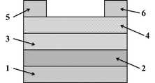
图1为本发明底栅顶接触式气体传感器结构示意图;Fig. 1 is a schematic structural diagram of a bottom-gate top-contact gas sensor of the present invention;
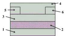
图2为本发明底栅底接触式气体传感器结构示意图;2 is a schematic structural diagram of a bottom-gate bottom-contact gas sensor of the present invention;
图3为本发明两种不同器件在不同二氧化氮氛围下的时间-源漏电流图,器件A未经极性溶剂处理,器件B为经极性溶剂处理;Fig. 3 is the time-source-leakage current diagram of two different devices of the present invention under different nitrogen dioxide atmospheres, device A is not processed by polar solvent, and device B is processed by polar solvent;
图中:1-衬底,2-栅电极,3-介电层,4-有机半导体层,5-源电极,6-漏电极。In the figure: 1-substrate, 2-gate electrode, 3-dielectric layer, 4-organic semiconductor layer, 5-source electrode, 6-drain electrode.
具体实施方式Detailed ways
基于有机薄膜晶体管二氧化硫气体传感器,包括衬底、栅电极、介电层、有机半导体、源电极和漏电极,所述介电层表面在形成其上的有机半导体层之前经过了极性溶剂处理。The sulfur dioxide gas sensor based on an organic thin film transistor includes a substrate, a gate electrode, a dielectric layer, an organic semiconductor, a source electrode and a drain electrode, and the surface of the dielectric layer is treated with a polar solvent before forming an organic semiconductor layer thereon.
衬底可采用刚性衬底或者柔性衬底,如硅片、玻璃、聚合物薄膜和金属箔中的一种,有一定的防水汽和氧气渗透的能力,有较好的表面平整度。The substrate can be a rigid substrate or a flexible substrate, such as one of silicon wafer, glass, polymer film and metal foil, which has a certain ability of waterproofing and oxygen penetration, and has better surface smoothness.
栅电极、源电极和漏电极采用具有低电阻的材料构成,如金(Au)、银(Ag)、镁(Mg)、铝(Al)、铜(Cu)、钙(Ca)、钡(Ba)、镍(Ni)等金属及其合金材料,金属氧化物,如氧化铟锡(ITO),氧化锌锡(IZO)导电薄膜和导电复合材料,如金胶、银胶、碳胶等,制备方法可以是真空热蒸镀、磁控溅射、等离子体增强的化学气相沉积、丝网印刷、打印、旋涂等各种沉积方法。所述源电极和漏电极的厚度为10~100 nm。The gate electrode, source electrode, and drain electrode are made of materials with low resistance, such as gold (Au), silver (Ag), magnesium (Mg), aluminum (Al), copper (Cu), calcium (Ca), barium (Ba ), nickel (Ni) and other metals and their alloy materials, metal oxides, such as indium tin oxide (ITO), zinc tin oxide (IZO) conductive films and conductive composite materials, such as gold glue, silver glue, carbon glue, etc., preparation The method can be various deposition methods such as vacuum thermal evaporation, magnetron sputtering, plasma-enhanced chemical vapor deposition, screen printing, printing, and spin coating. The thickness of the source electrode and the drain electrode is 10-100 nm.
栅极介电层采用具有良好的介电性能的材料,无机绝缘材料如二氧化硅(SiO2)、氮化硅(Si3N4)、氧化铝(A12O3) 、氟化锂(LiF)、二氧化钛(TiO2)、二氧化铪(HfO2)、五氧化二坦(Ta2O5);有机绝缘材料如聚乙烯醇(PVA)、聚氯乙烯(PVC)、聚乙烯吡咯烷酮(PVP)、聚苯乙烯(PS)、聚甲基丙烯酸甲酯(PMMA)、聚乙基丙烯酸酯(PCA)、聚四氟乙烯(PTFE)、聚酰亚胺(PI)或聚乙烯(PE)等,制备方法可以是等离子体增强的化学气相沉积、热氧化、旋涂或者真空蒸镀等。所述栅极介电层的厚度为5~2000 nm。The gate dielectric layer is made of materials with good dielectric properties, inorganic insulating materials such as silicon dioxide (SiO2), silicon nitride (Si3N4), aluminum oxide (A12O3), lithium fluoride (LiF), titanium dioxide (TiO2) , hafnium dioxide (HfO2), pentoxide (Ta2O5); organic insulating materials such as polyvinyl alcohol (PVA), polyvinyl chloride (PVC), polyvinylpyrrolidone (PVP), polystyrene (PS), polymethyl Methyl acrylate (PMMA), polyethyl acrylate (PCA), polytetrafluoroethylene (PTFE), polyimide (PI) or polyethylene (PE), etc., the preparation method can be plasma-enhanced chemical vapor phase Deposition, thermal oxidation, spin coating or vacuum evaporation, etc. The thickness of the gate dielectric layer is 5-2000 nm.
有机半导体探测层采用并四苯、并五苯,及其具有取代基的衍生物、6,13-二三异丙酯硅基乙炔并五苯、低聚噻吩,其包含连接在噻吩环的第2及5位置的四至八个噻吩、茈四甲酸二酐(PTCDA)、萘四甲酸二酐(NTCDA)、酞菁铜、酞菁锌、酞菁钴、金属化酞菁及其卤代衍生物fluorinated copper phthalocyanine (F16CuPc)、酞菁铜(CuPc)、亚噻吩基和1,2-亚乙烯基的低共聚物和共聚物、富勒烯C60及其衍生物、苝Perylene及其衍生物、Alpha-六噻吩、红荧烯(Rubrene)、聚噻吩Polythiophene或聚3-己基拿吩poly(3-hexyithiophene)等,制备方法可以是等离子体增强的化学气相沉积、热氧化、旋涂、真空蒸镀、滴膜、压印、印刷或气喷等。所述有机半导体探测层的厚度均为2~100 nm。The organic semiconductor detection layer uses naphthacene, pentacene, and its derivatives with substituents, 6,13-ditriisopropyl silylacetylene pentacene, and oligothiophene, which contain the first Four to eight thiophenes at
极性溶剂处理的方式中,极性溶剂包括水、甲酰胺、三氟乙酸、二甲基亚砜、乙腈二甲基甲酰胺、六甲基磷酰胺、甲醇、乙醇、乙酸、异丙醇、吡啶、四甲基乙二胺、丙酮、三乙胺、正丁醇、二氧六环、四氢呋喃、甲酸甲酯、三丁氨、甲乙酮、乙酸乙酯、三辛胺、碳酸二甲酯、乙醚、异丙醚、苯甲醚、正丁醚、三氯乙烯、二苯醚、二氯甲烷或三氯甲烷。处理方式包括溶剂浸泡或溶剂蒸熏。溶剂浸泡时间为10~10000秒,溶剂熏蒸的时间为1~300分钟。In the way of polar solvent treatment, polar solvents include water, formamide, trifluoroacetic acid, dimethyl sulfoxide, acetonitrile dimethylformamide, hexamethylphosphoramide, methanol, ethanol, acetic acid, isopropanol, Pyridine, tetramethylethylenediamine, acetone, triethylamine, n-butanol, dioxane, tetrahydrofuran, methyl formate, tributylamine, methyl ethyl ketone, ethyl acetate, trioctylamine, dimethyl carbonate, ether , isopropyl ether, anisole, n-butyl ether, trichloroethylene, diphenyl ether, methylene chloride or chloroform. Treatment methods include solvent immersion or solvent fumigation. The solvent immersion time is 10-10000 seconds, and the solvent fumigation time is 1-300 minutes.
极性溶剂处理作为一种简单实用的表面处理方法,在诸多方面都有广泛的应用,如:经溶剂处理的有机薄膜太阳能电池界面,能使有机薄膜太阳能电池的效率达到有效的提升;在聚合物的制备等方面起到辅助作用,已实现快速高效的聚合物合成。极性溶剂处理已经被证实对有机薄膜晶体管的介电层能达到很好的改性作用。经过极性溶剂处理的介电层表面能够实现表面能改变、表面材料组分的重组或表面形貌优化的作用,因此,基于介电层经极性溶剂处理的有机薄膜晶体管传感器相对于传统的未经极性溶剂处理晶体管传感器将在灵敏度、选择性、稳定性以及响应时间等方面有着巨大的提升空间。As a simple and practical surface treatment method, polar solvent treatment has been widely used in many aspects, such as: solvent-treated organic thin film solar cell interface can effectively improve the efficiency of organic thin film solar cells; It plays an auxiliary role in the preparation of polymers and has achieved rapid and efficient polymer synthesis. Polar solvent treatment has been proven to achieve a good modification effect on the dielectric layer of organic thin film transistors. The surface of the dielectric layer treated with a polar solvent can change the surface energy, reorganize the surface material components or optimize the surface morphology. Therefore, the organic thin film transistor sensor based on the dielectric layer treated with a polar solvent is relatively Transistor sensors without polar solvent treatment will have huge room for improvement in terms of sensitivity, selectivity, stability, and response time.
以下结合附图对本发明作进一步的说明。The present invention will be further described below in conjunction with the accompanying drawings.
实施例1Example 1
如图1所示为底栅顶接触式结构。器件各层的材料和厚度为:衬底1为玻璃,栅电极2为ITO,厚度为120 nm,栅极介电层3为PS,厚度为500 nm,其中介电层3在乙醚溶剂中浸泡10秒,有机半导体为并五苯,厚度为2 nm,源电极5和漏电极6均为Au,厚度为10 nm。As shown in Figure 1, it is a bottom-gate top-contact structure. The material and thickness of each layer of the device are as follows: the
制备方法如下:The preparation method is as follows:
①对溅射好栅电极ITO的玻璃衬底1进行彻底的清洗,清洗后用干燥氮气吹干;① Thoroughly clean the
②采用旋涂法在ITO上制备PS薄膜形成栅极介电层3;② Prepare a PS film on the ITO by spin coating to form the
③对旋涂好的PS薄膜经行加热烘烤;③The spin-coated PS film is heated and baked;
④对介电层3在乙醚溶剂中浸泡10秒;④ Soak the
⑤采用真空蒸镀制备并五苯有机半导体层4;⑤ Prepare the pentacene
⑥采用真空蒸镀制备源电极5和漏电极6。⑥ Prepare the
实施例2Example 2
如图1所示,传感器各层的材料和厚度为:衬底1为玻璃,栅电极2为ITO,厚度为120 nm,栅极介电层3为PMMA,厚度为200 nm,其中介电层3在异丙醇蒸汽下蒸熏1分钟,有机半导体探测层4为酞菁铜,厚度为10 nm,源电极5和漏电极6均为Au,厚度为50 nm。As shown in Figure 1, the material and thickness of each layer of the sensor are as follows: the
制备方法如下:The preparation method is as follows:
①对溅射好栅电极ITO的玻璃衬底1进行彻底的清洗,清洗后用干燥氮气吹干;① Thoroughly clean the
②采用旋涂法在ITO上制备PMMA薄膜形成栅极介电层3;② Preparing PMMA film on ITO by spin coating method to form
③对旋涂好的PMMA薄膜经行加热烘烤;③Heating and baking the spin-coated PMMA film;
④对介电层3在异丙醇蒸汽下蒸熏1分钟;④ Fumigate the
⑤采用真空蒸镀制备酞菁铜有机半导体层4;⑤ Prepare copper phthalocyanine
⑥采用真空蒸镀制备源电极5和漏电极6。⑥ Prepare the
实施例3Example 3
如图1所示,传感器各层的材料和厚度为:衬底1为玻璃,栅电极2为ITO,厚度为120 nm,栅极介电层3为PVA,厚度为2000 nm,其中介电层3在三氯甲烷溶剂中浸泡60秒,有机半导体探测层4为六噻吩,厚度为25 nm,源电极5和漏电极6均为Au,厚度为50 nm。As shown in Figure 1, the material and thickness of each layer of the sensor are as follows: the
制备方法如下:The preparation method is as follows:
①对溅射好栅电极ITO的玻璃衬底1进行彻底的清洗,清洗后用干燥氮气吹干;① Thoroughly clean the
②采用旋涂法在ITO上制备PVA薄膜形成栅极介电层3;② Preparing a PVA film on the ITO by spin coating to form the
③对旋涂好的PVA薄膜经行加热烘烤;③The spin-coated PVA film is heated and baked;
④将介电层3放置在三氯甲烷溶剂中浸泡60秒;④ Soak the
⑤采用真空蒸镀制备六噻吩有机半导体层4;⑤ Prepare the hexathiophene
⑥采用真空蒸镀制备源电极5和漏电极6。⑥ Prepare the
实施例4Example 4
如图2所示,传感器各层的材料和厚度为:衬底1为硅片,栅电极2为硅,栅极介电层3为二氧化硅,厚度为5 nm,其中介电层3在丙酮溶剂中浸泡10000秒,源电极5和漏电极6均为Au,厚度为50 nm,有机半导体探测层4为红荧烯,厚度为25 nm。As shown in Figure 2, the material and thickness of each layer of the sensor are: the
其制备方法如下:Its preparation method is as follows:
①对硅为栅电极的衬底1进行彻底的清洗,清洗后用干燥氮气吹干;① Thoroughly clean the
②采用热氧化或者气相沉积的方法生成一层SiO2作为栅极介电层3;② A layer of SiO2 is formed as the
③对介电层3在丙酮溶剂中浸泡10000秒;③ Soak the
④在SiO2表面通过真空蒸镀或者溅射的方法制备源电极5和漏电极6;④Preparing the
⑤采用真空蒸镀制备红荧烯有机半导体层4。⑤ Prepare the rubrene
实施例5Example 5
如图2所示,传感器各层的材料和厚度为:衬底1为硅片,栅电极2为硅,栅极介电层3为聚乙烯吡咯烷酮,厚度为100 nm,其中介电层3在四氢呋喃蒸汽中蒸熏2分钟,源电极5和漏电极6均为Ag,厚度为50 nm,有机半导体探测层4为F16CuPc,厚度为25 nm。As shown in Figure 2, the material and thickness of each layer of the sensor are: the
其制备方法如下:Its preparation method is as follows:
①对硅为栅电极的衬底1进行彻底的清洗,清洗后用干燥氮气吹干;① Thoroughly clean the
②采用旋涂法在ITO上制备聚乙烯吡咯烷酮薄膜形成栅极介电层3;② Prepare polyvinylpyrrolidone film on ITO by spin coating method to form
③对旋涂好的聚乙烯吡咯烷酮薄膜经行加热烘烤;③The spin-coated polyvinylpyrrolidone film is heated and baked;
③对介电层3在四氢呋喃蒸汽中蒸熏2分钟;③
④在聚乙烯吡咯烷酮表面通过真空蒸镀或者溅射的方法制备源电极5和漏电极6;④ Prepare
⑤采用真空蒸镀制备F16CuPc有机半导体层4。⑤ Prepare the F16 CuPc
实施例6Example 6
如图1所示,传感器各层的材料和厚度为:衬底1为玻璃,栅电极2为ITO,厚度为120 nm,栅极介电层3为三氧化二铝,厚度为50 nm,其中介电层3在乙酸乙酯蒸汽中蒸熏300分钟,有机半导体探测层4为富勒烯,厚度为25 nm,源电极5和漏电极6均为Ag,厚度为30 nm。As shown in Figure 1, the material and thickness of each layer of the sensor are as follows: the
制备方法如下:The preparation method is as follows:
①对溅射好栅电极ITO的玻璃衬底1进行彻底的清洗,清洗后用干燥氮气吹干;① Thoroughly clean the
②采用反应磁控溅射在ITO上制备三氧化二铝薄膜形成栅极介电层3;②Using reactive magnetron sputtering to prepare aluminum oxide film on ITO to form
③将介电层3在乙酸乙酯蒸汽中蒸熏300分钟;③ Fumigate the
④采用真空蒸镀制备富勒烯有机半导体层4;④Preparing the fullerene
⑤采用真空蒸镀制备源电极5和漏电极6。⑤ Prepare the
实施例7Example 7
如图2所示,传感器各层的材料和厚度为:衬底1为玻璃,栅电极2为ITO,厚度为120 nm,栅极介电层3为氮化硅,厚度为20 nm,其中介电层3在三丁氨溶液中浸泡500秒,源电极5和漏电极6均为Cu,厚度为100 nm,有机半导体探测层4为并五苯,厚度为100 nm。As shown in Figure 2, the material and thickness of each layer of the sensor are as follows: the
制备方法如下:The preparation method is as follows:
①对溅射好栅电极ITO的玻璃衬底1进行彻底的清洗,清洗后用干燥氮气吹干;① Thoroughly clean the
②采用反应磁控溅射在ITO上制备氮化硅薄膜形成栅极介电层3;② Using reactive magnetron sputtering to prepare silicon nitride film on ITO to form
③将介电层3在三丁氨溶液中浸泡500秒;③ Soak the
④在氮化硅表面通过真空蒸镀或者溅射的方法制备源电极5和漏电极6;④ Prepare the
⑤采用真空蒸镀制备并五苯有机半导体层4。⑤ Prepare the pentacene
本发明已经通过上述实施例进行了说明,但应当理解的是,上述实施例只是用于举例和说明的目的,而非意在将本发明限制于所描述的实施例范围内。此外本领域技术人员可以理解的是,本发明并不局限于上述实施例,根据本发明的教导还可以做出更多种的变型和修改,这些变型和修改均落在本发明所要求保护的范围以内。本发明的保护范围由附属的权利要求书及其等效范围所界定。 The present invention has been described through the above-mentioned embodiments, but it should be understood that the above-mentioned embodiments are only for the purpose of illustration and description, and are not intended to limit the present invention to the scope of the described embodiments. In addition, those skilled in the art can understand that the present invention is not limited to the above-mentioned embodiments, and more variations and modifications can be made according to the teachings of the present invention, and these variations and modifications all fall within the claimed scope of the present invention. within the range. The protection scope of the present invention is defined by the appended claims and their equivalent scope. the
Claims (10)
Translated fromChinesePriority Applications (1)
| Application Number | Priority Date | Filing Date | Title |
|---|---|---|---|
| CN201310657575.6ACN103630577A (en) | 2013-12-09 | 2013-12-09 | Preparation method of OTFT(organic thin-film transistor)-based sulfur dioxide gas sensor |
Applications Claiming Priority (1)
| Application Number | Priority Date | Filing Date | Title |
|---|---|---|---|
| CN201310657575.6ACN103630577A (en) | 2013-12-09 | 2013-12-09 | Preparation method of OTFT(organic thin-film transistor)-based sulfur dioxide gas sensor |
Publications (1)
| Publication Number | Publication Date |
|---|---|
| CN103630577Atrue CN103630577A (en) | 2014-03-12 |
Family
ID=50211850
Family Applications (1)
| Application Number | Title | Priority Date | Filing Date |
|---|---|---|---|
| CN201310657575.6APendingCN103630577A (en) | 2013-12-09 | 2013-12-09 | Preparation method of OTFT(organic thin-film transistor)-based sulfur dioxide gas sensor |
Country Status (1)
| Country | Link |
|---|---|
| CN (1) | CN103630577A (en) |
Cited By (4)
| Publication number | Priority date | Publication date | Assignee | Title |
|---|---|---|---|---|
| CN104132989A (en)* | 2014-08-01 | 2014-11-05 | 电子科技大学 | Organic field-effect tube gas sensor based on mixed insulating layer and preparation method thereof |
| CN108447915A (en)* | 2018-03-02 | 2018-08-24 | 华中科技大学 | A kind of thin film field effect transistor type gas sensor and its preparation method |
| CN111505089A (en)* | 2020-04-24 | 2020-08-07 | 电子科技大学 | A kind of sulfur dioxide sensor based on organic field effect transistor and preparation method thereof |
| CN112736199A (en)* | 2019-10-28 | 2021-04-30 | 天津大学 | C8-BTBT single crystal film, preparation method thereof and organic field effect transistor based on C8-BTBT single crystal film |
Citations (4)
| Publication number | Priority date | Publication date | Assignee | Title |
|---|---|---|---|---|
| US20090256215A1 (en)* | 2005-03-18 | 2009-10-15 | Nano-Proprietary, Inc. | Gated metal oxide sensor |
| CN102507659A (en)* | 2011-11-28 | 2012-06-20 | 电子科技大学 | Methanol gas sensor based on organic filter transistor and preparation method of methanol gas sensor |
| CN103311313A (en)* | 2013-06-21 | 2013-09-18 | 华南理工大学 | Oxide thin film transistor and preparation method thereof |
| CN103399072A (en)* | 2013-08-02 | 2013-11-20 | 中国科学院化学研究所 | Gas-assisted organic field-effect transistor sensor, and preparation method and applications thereof |
- 2013
- 2013-12-09CNCN201310657575.6Apatent/CN103630577A/enactivePending
Patent Citations (4)
| Publication number | Priority date | Publication date | Assignee | Title |
|---|---|---|---|---|
| US20090256215A1 (en)* | 2005-03-18 | 2009-10-15 | Nano-Proprietary, Inc. | Gated metal oxide sensor |
| CN102507659A (en)* | 2011-11-28 | 2012-06-20 | 电子科技大学 | Methanol gas sensor based on organic filter transistor and preparation method of methanol gas sensor |
| CN103311313A (en)* | 2013-06-21 | 2013-09-18 | 华南理工大学 | Oxide thin film transistor and preparation method thereof |
| CN103399072A (en)* | 2013-08-02 | 2013-11-20 | 中国科学院化学研究所 | Gas-assisted organic field-effect transistor sensor, and preparation method and applications thereof |
Non-Patent Citations (3)
| Title |
|---|
| 刘翔等: "有机薄膜晶体管(OTFT)的研究进展", 《现代显示》, no. 82, 30 September 2007 (2007-09-30), pages 54 - 60* |
| 徐巍东等: "水溶性共轭聚合物研究与应用进展", 《中国科学:化学》, vol. 41, no. 3, 31 December 2011 (2011-12-31)* |
| 田雪雁等: "高分子有机场效应晶体管中半导体薄膜结晶行为及微观结构变化的研究", 《物理学报》, vol. 60, no. 2, 31 December 2011 (2011-12-31)* |
Cited By (6)
| Publication number | Priority date | Publication date | Assignee | Title |
|---|---|---|---|---|
| CN104132989A (en)* | 2014-08-01 | 2014-11-05 | 电子科技大学 | Organic field-effect tube gas sensor based on mixed insulating layer and preparation method thereof |
| CN108447915A (en)* | 2018-03-02 | 2018-08-24 | 华中科技大学 | A kind of thin film field effect transistor type gas sensor and its preparation method |
| CN112736199A (en)* | 2019-10-28 | 2021-04-30 | 天津大学 | C8-BTBT single crystal film, preparation method thereof and organic field effect transistor based on C8-BTBT single crystal film |
| CN112736199B (en)* | 2019-10-28 | 2023-03-24 | 天津大学 | C8-BTBT (British Bittery-based) single crystal film, preparation method thereof and organic field effect transistor based on C8-BTBT single crystal film |
| CN111505089A (en)* | 2020-04-24 | 2020-08-07 | 电子科技大学 | A kind of sulfur dioxide sensor based on organic field effect transistor and preparation method thereof |
| CN111505089B (en)* | 2020-04-24 | 2021-08-10 | 电子科技大学 | Sulfur dioxide sensor based on organic field effect transistor and preparation method thereof |
Similar Documents
| Publication | Publication Date | Title |
|---|---|---|
| CN103630576A (en) | Preparation method of OTFT(organic thin-film transistor)-based nitrogen dioxide gas sensor | |
| CN103604835A (en) | Preparation method of organic thin film transistor-based carbon monoxide gas sensor | |
| CN105510389A (en) | A kind of humidity sensor based on organic field effect transistor and preparation method thereof | |
| Yi et al. | The mechanical bending effect and mechanism of high performance and low-voltage flexible organic thin-film transistors with a cross-linked PVP dielectric layer | |
| CN107104189A (en) | perovskite thin film solar cell and preparation method thereof | |
| CN102507659A (en) | Methanol gas sensor based on organic filter transistor and preparation method of methanol gas sensor | |
| King et al. | Review of recent advances and sensing mechanisms in solid-state organic thin-film transistor (OTFT) sensors | |
| CN106198635A (en) | A kind of humidity sensor based on organic field effect tube and preparation method thereof | |
| CN103399072B (en) | Gas-assisted organic field-effect transistor sensor, and preparation method and applications thereof | |
| CN101295765A (en) | A kind of organic field effect transistor and its preparation method and application | |
| CN106706718A (en) | Three-layer-structure sensitive layer phthalocyanine gas sensitive sensor and preparation method thereof | |
| CN103630577A (en) | Preparation method of OTFT(organic thin-film transistor)-based sulfur dioxide gas sensor | |
| CN108831996A (en) | A three-layer heterojunction organic field effect transistor memory and its preparation method | |
| CN108470852A (en) | A kind of preparation method of modifying interface perovskite solar cell | |
| CN109411606B (en) | A thin film preparation process and a gas sensor preparation method related to the process | |
| CN107565020A (en) | A formaldehyde sensor based on an organic field effect tube and its preparation method | |
| CN108287189B (en) | A kind of organic field effect tube humidity sensor based on synergistic effect and preparation method thereof | |
| CN112051316A (en) | Ammonia gas sensor based on organic thin film transistor and preparation method thereof | |
| CN105301055B (en) | A kind of organic field-effect tube nitrogen dioxide sensor | |
| CN102332534A (en) | A kind of N-type organic thin film transistor and its preparation method | |
| TWI453964B (en) | Organic thin film transistor | |
| CN106226378A (en) | A kind of nitrogen dioxide sensor being embedded with fluoropolymer and preparation method thereof | |
| CN111505089A (en) | A kind of sulfur dioxide sensor based on organic field effect transistor and preparation method thereof | |
| CN103746075B (en) | A kind of method for improving stability of organic thin-film transistor | |
| CN102636552A (en) | A methane gas sensor based on an organic thin film transistor and its preparation method |
Legal Events
| Date | Code | Title | Description |
|---|---|---|---|
| PB01 | Publication | ||
| PB01 | Publication | ||
| C10 | Entry into substantive examination | ||
| SE01 | Entry into force of request for substantive examination | ||
| RJ01 | Rejection of invention patent application after publication | ||
| RJ01 | Rejection of invention patent application after publication | Application publication date:20140312 |