CN103578954A - Semiconductor integrated circuit with metal gate - Google Patents
Semiconductor integrated circuit with metal gateDownload PDFInfo
- Publication number
- CN103578954A CN103578954ACN201210495541.7ACN201210495541ACN103578954ACN 103578954 ACN103578954 ACN 103578954ACN 201210495541 ACN201210495541 ACN 201210495541ACN 103578954 ACN103578954 ACN 103578954A
- Authority
- CN
- China
- Prior art keywords
- gate trench
- stack
- metal
- dfm
- gate
- Prior art date
- Legal status (The legal status is an assumption and is not a legal conclusion. Google has not performed a legal analysis and makes no representation as to the accuracy of the status listed.)
- Granted
Links
Images


Classifications
- H—ELECTRICITY
- H10—SEMICONDUCTOR DEVICES; ELECTRIC SOLID-STATE DEVICES NOT OTHERWISE PROVIDED FOR
- H10D—INORGANIC ELECTRIC SEMICONDUCTOR DEVICES
- H10D64/00—Electrodes of devices having potential barriers
- H10D64/01—Manufacture or treatment
- H10D64/017—Manufacture or treatment using dummy gates in processes wherein at least parts of the final gates are self-aligned to the dummy gates, i.e. replacement gate processes
- H—ELECTRICITY
- H10—SEMICONDUCTOR DEVICES; ELECTRIC SOLID-STATE DEVICES NOT OTHERWISE PROVIDED FOR
- H10D—INORGANIC ELECTRIC SEMICONDUCTOR DEVICES
- H10D30/00—Field-effect transistors [FET]
- H10D30/01—Manufacture or treatment
- H10D30/021—Manufacture or treatment of FETs having insulated gates [IGFET]
- H—ELECTRICITY
- H10—SEMICONDUCTOR DEVICES; ELECTRIC SOLID-STATE DEVICES NOT OTHERWISE PROVIDED FOR
- H10D—INORGANIC ELECTRIC SEMICONDUCTOR DEVICES
- H10D30/00—Field-effect transistors [FET]
- H10D30/60—Insulated-gate field-effect transistors [IGFET]
- H—ELECTRICITY
- H10—SEMICONDUCTOR DEVICES; ELECTRIC SOLID-STATE DEVICES NOT OTHERWISE PROVIDED FOR
- H10D—INORGANIC ELECTRIC SEMICONDUCTOR DEVICES
- H10D64/00—Electrodes of devices having potential barriers
- H10D64/60—Electrodes characterised by their materials
- H10D64/66—Electrodes having a conductor capacitively coupled to a semiconductor by an insulator, e.g. MIS electrodes
- H10D64/667—Electrodes having a conductor capacitively coupled to a semiconductor by an insulator, e.g. MIS electrodes the conductor comprising a layer of alloy material, compound material or organic material contacting the insulator, e.g. TiN workfunction layers
- H—ELECTRICITY
- H10—SEMICONDUCTOR DEVICES; ELECTRIC SOLID-STATE DEVICES NOT OTHERWISE PROVIDED FOR
- H10D—INORGANIC ELECTRIC SEMICONDUCTOR DEVICES
- H10D64/00—Electrodes of devices having potential barriers
- H10D64/60—Electrodes characterised by their materials
- H10D64/66—Electrodes having a conductor capacitively coupled to a semiconductor by an insulator, e.g. MIS electrodes
- H10D64/68—Electrodes having a conductor capacitively coupled to a semiconductor by an insulator, e.g. MIS electrodes characterised by the insulator, e.g. by the gate insulator
- H10D64/691—Electrodes having a conductor capacitively coupled to a semiconductor by an insulator, e.g. MIS electrodes characterised by the insulator, e.g. by the gate insulator comprising metallic compounds, e.g. metal oxides or metal silicates
Landscapes
- Insulated Gate Type Field-Effect Transistor (AREA)
- Metal-Oxide And Bipolar Metal-Oxide Semiconductor Integrated Circuits (AREA)
Abstract
Translated fromChinese
Description
Translated fromChinese技术领域technical field
本发明涉及半导体集成电路,具体而言,涉及具有金属栅极的半导体集成电路。The present invention relates to semiconductor integrated circuits, and more particularly, to semiconductor integrated circuits having metal gates.
背景技术Background technique
半导体集成电路(IC)产业经历了指数性增长。在IC设计和材料上的技术改进产生了一代又一代的IC,其中,每一代都具有比前一代更小更复杂的电路。在IC的发展过程中,随着几何尺寸(即,可以使用制造工艺制造的最小元件(或线))的减小,功能密度(即,每芯片面积的互连器件的数目)普遍增大。The semiconductor integrated circuit (IC) industry has experienced exponential growth. Technological improvements in IC design and materials have produced successive generations of ICs, where each generation has smaller and more complex circuits than the previous generation. During the evolution of ICs, functional density (ie, the number of interconnected devices per chip area) has generally increased as geometry size (ie, the smallest component (or line) that can be made using a fabrication process) has decreased.
这种按比例缩小工艺通常通过提高生产效率以及降低相关成本提供收益。这种按比例缩小也提高了IC加工和制造的复杂度。为了实现这些改进,需要在IC加工和制造上的类似发展。例如,诸如金属氧化物半导体场效应晶体管(MOSFET)的半导体器件通过各种技术节点按比例缩小,高介电常数(HK)材料和金属栅极(MG)通常被考虑形成用于场效应晶体管(FET)的栅极堆叠件。在形成MG时发生集成问题,诸如需要使MG蚀刻工艺中的功函数(WF)金属与填充金属匹配。需要在这个领域有所改进。This scaling down process typically provides benefits through increased production efficiency and reduced associated costs. This scaling down also increases the complexity of IC processing and manufacturing. To achieve these improvements, similar developments in IC processing and manufacturing are required. For example, semiconductor devices such as metal-oxide-semiconductor field-effect transistors (MOSFETs) are scaled down through various technology nodes, and high dielectric constant (HK) materials and metal gates (MG) are often considered for formation of field-effect transistors ( FET) gate stack. Integration issues arise when forming the MG, such as the need to match the work function (WF) metal to the fill metal in the MG etch process. Improvements are needed in this area.
发明内容Contents of the invention
为了解决现有技术中存在的问题,根据本发明的一个方面,提供了一种制造半导体集成电路(IC)的方法,所述方法包括:提供具有栅极沟槽的半导体衬底;用功函数(WF)金属堆叠件部分填充所述栅极沟槽;在所述WF金属堆叠件上方用伪填充材料(DFM)填充剩余的栅极沟槽;保留所述DFM的同时在所述栅极沟槽中形成子栅极沟槽;用绝缘体保护层填充所述子栅极沟槽,从而在所述栅极沟槽中形成绝缘区;完全去除所述DFM,从而在所述栅极沟槽的中心形成MG中心沟槽(MGCT);以及用填充金属填充所述MGCT。In order to solve the problems in the prior art, according to one aspect of the present invention, a method of manufacturing a semiconductor integrated circuit (IC) is provided, the method comprising: providing a semiconductor substrate with a gate trench; a work function ( WF) a metal stack partially filling the gate trench; filling the remaining gate trench with a dummy fill material (DFM) over the WF metal stack; filling the gate trench while retaining the DFM forming a sub-gate trench; filling the sub-gate trench with an insulator protective layer, thereby forming an insulating region in the gate trench; completely removing the DFM, thereby forming an insulating region in the center of the gate trench forming an MG center trench (MGCT); and filling the MGCT with a fill metal.
在上述方法中,其中,所述半导体衬底包括:位于所述半导体衬底上的界面层(IL);位于所述IL上方的高k(HK)介电层;以及作为所述栅极沟槽的侧壁的侧壁间隔件。In the above method, wherein the semiconductor substrate comprises: an interfacial layer (IL) on the semiconductor substrate; a high-k (HK) dielectric layer above the IL; and as the gate trench Sidewall spacers for the sidewalls of the tank.
在上述方法中,其中,所述子栅极沟槽通过蚀刻工艺形成,所述蚀刻工艺具有相对于所述DFM的蚀刻选择性,其中,所述DFM在所述蚀刻工艺中至少部分地保持完好。In the above method, wherein the sub-gate trench is formed by an etching process having an etching selectivity relative to the DFM, wherein the DFM remains at least partially intact during the etching process .
在上述方法中,其中,所述蚀刻工艺去除所述WF金属堆叠件的一部分,从而形成具有自对准特性的所述子栅极沟槽。In the above method, wherein, the etching process removes a part of the WF metal stack, thereby forming the sub-gate trenches with self-alignment characteristics.
在上述方法中,其中,所述DFM包括介电材料。In the above method, wherein the DFM includes a dielectric material.
在上述方法中,其中,通过凹进所述WF金属堆叠件和所述HK介电层形成所述子栅极沟槽。In the above method, wherein the sub-gate trench is formed by recessing the WF metal stack and the HK dielectric layer.
在上述方法中,其中,通过凹进所述WF金属堆叠件,所述HK介电层以及所述侧壁间隔件形成所述子栅极沟槽。In the above method, wherein the sub-gate trenches are formed by recessing the WF metal stack, the HK dielectric layer and the sidewall spacers.
在上述方法中,其中,控制所述子栅极沟槽的深度(d)以达到器件性能的预定目标。In the above method, wherein the depth (d) of the sub-gate trench is controlled to achieve a predetermined target of device performance.
在上述方法中,进一步包括:在用所述绝缘体保护层填充所述子栅极沟槽之后,使用化学机械抛光(CMP)去除所述绝缘体保护层的多余部分以暴露所述DFM的顶面。In the above method, it further includes: after filling the sub-gate trenches with the insulator protection layer, using chemical mechanical polishing (CMP) to remove excess parts of the insulator protection layer to expose the top surface of the DFM.
在上述方法中,其中,所述绝缘体保护层包括与所述DFM相比具有基本上不同的蚀刻速率的材料。In the above method, wherein the insulator protection layer comprises a material having a substantially different etch rate than the DFM.
在上述方法中,其中,通过回蚀工艺去除所述DFM,所述回蚀工艺具有相对于所述绝缘体保护层的蚀刻选择性。In the above method, wherein the DFM is removed by an etch-back process, the etch-back process has an etch selectivity relative to the insulator protection layer.
在上述方法中,进一步包括:在用所述填充金属填充所述MGCT之后,使用CMP去除多余的填充金属以达到预定的填充金属高度(h)。In the above method, it further includes: after filling the MGCT with the filling metal, using CMP to remove excess filling metal to reach a predetermined filling metal height (h).
根据本发明的另一方面,还提供了一种半导体集成电路(IC),所述IC包括:半导体衬底;在所述半导体衬底上形成的栅极介电堆叠件;在所述栅极介电堆叠件上方形成的金属栅极(MG)堆叠件;其中,所述MG堆叠件具有被边缘区域围绕的中心区域;在所述MG堆叠件的中心区域的上部中形成的填充金属;在所述MG堆叠件的边缘区域的上部中形成的绝缘区;以及在所述MG堆叠件的中心区域和边缘区域的下部中形成的功函数(WF)金属堆叠件。According to another aspect of the present invention, there is also provided a semiconductor integrated circuit (IC), the IC comprising: a semiconductor substrate; a gate dielectric stack formed on the semiconductor substrate; a metal gate (MG) stack formed over a dielectric stack; wherein the MG stack has a central region surrounded by edge regions; a fill metal formed in an upper portion of the central region of the MG stack; an insulating region formed in an upper portion of an edge region of the MG stack; and a work function (WF) metal stack formed in a central region and a lower portion of an edge region of the MG stack.
在上述IC中,其中,所述栅极介电堆叠件包括:位于所述半导体衬底上的界面层(IL);以及位于所述IL上方的高k(HK)介电层。In the above IC, wherein the gate dielectric stack includes: an interfacial layer (IL) on the semiconductor substrate; and a high-k (HK) dielectric layer over the IL.
在上述IC中,进一步包括:位于所述MG堆叠件和所述栅极介电堆叠件上的侧壁间隔件。In the above IC, further comprising: a sidewall spacer on the MG stack and the gate dielectric stack.
根据本发明的又一方面,还提供了一种制造半导体集成电路(IC)的方法,所述方法包括:提供半导体衬底;在所述半导体衬底上形成伪栅极;在所述伪栅极上形成侧壁间隔件;去除所述伪栅极以形成栅极沟槽;用功函数(WF)金属堆叠件部分地填充所述栅极沟槽;用伪填充材料(DFM)在所述WF金属堆叠件上方填充剩余的栅极沟槽;在所述栅极沟槽中形成围绕所述DFM的具有预定深度(d)的子栅极沟槽;用绝缘体保护层填充所述子栅极沟槽以在所述栅极沟槽中形成绝缘区;在所述绝缘区形成之后,从所述栅极沟槽完全去除所述DFM,从而在所述栅极沟槽中形成MG中心沟槽(MGCT);用填充金属填充所述MGCT;以及回蚀所述填充金属至预定的金属高度(h)。According to still another aspect of the present invention, there is also provided a method of manufacturing a semiconductor integrated circuit (IC), the method comprising: providing a semiconductor substrate; forming a dummy gate on the semiconductor substrate; forming sidewall spacers on the electrodes; removing the dummy gates to form gate trenches; partially filling the gate trenches with work function (WF) metal stacks; filling the gate trenches with dummy fill material (DFM) filling the remaining gate trench above the metal stack; forming a sub-gate trench with a predetermined depth (d) around the DFM in the gate trench; filling the sub-gate trench with an insulator protection layer trench to form an insulating region in the gate trench; after the insulating region is formed, the DFM is completely removed from the gate trench, thereby forming a MG central trench in the gate trench ( MGCT); filling the MGCT with a fill metal; and etching back the fill metal to a predetermined metal height (h).
在上述方法中,其中,所述DFM包括相对于所述WF金属堆叠件的材料具有基本上不同的蚀刻速率的材料。In the above method, wherein the DFM comprises a material having a substantially different etch rate relative to a material of the WF metal stack.
在上述方法中,其中,在所述子栅极沟槽的形成过程中,所述DFM保持相当完好。In the above method, wherein, during the formation of the sub-gate trenches, the DFM remains relatively intact.
在上述方法中,其中,所述绝缘区由相对于所述DFM具有基本上不同的蚀刻速率的材料形成。In the above method, wherein the insulating region is formed of a material having a substantially different etch rate relative to the DFM.
在上述方法中,其中,在所述DFM去除过程中,所述绝缘区保持完好。In the above method, wherein, during the DFM removal process, the insulating region remains intact.
附图说明Description of drawings
当结合附图进行阅读时,根据下面详细的描述将更好地理解本发明。应该强调,根据工业中的标准实践,各种部件没有被按比例绘制并且仅仅用于说明的目的。实际上,为了清楚的讨论,各种部件的规格可能被任意增大或缩小。The present invention is better understood from the following detailed description when read with the accompanying drawings. It should be emphasized that, in accordance with the standard practice in the industry, various features are not drawn to scale and are used for illustration purposes only. In fact, the dimensions of the various components may be arbitrarily expanded or reduced for clarity of discussion.
图1是制造根据本发明的各方面所构造的半导体集成电路(IC)的示例方法的流程图。1 is a flowchart of an example method of fabricating a semiconductor integrated circuit (IC) constructed in accordance with aspects of the present invention.
图2A至图11是根据图1所述的方法构造的示例半导体集成电路(IC)在各个制造阶段的截面图。2A through 11 are cross-sectional views at various stages of fabrication of an example semiconductor integrated circuit (IC) constructed according to the method described in FIG. 1 .
具体实施方式Detailed ways
应该理解,为了实施本发明的不同部件,以下公开提供了许多不同的实施例或示例。以下描述元件和布置的特定示例以简化本公开。当然这些仅仅是示例并不打算限定。此外,在以下描述中,在第二工艺之前实施第一工艺可能包括其中第二工艺在第一工艺之后立即实施的实施例,还可能包括其中额外的工艺可能在第一和第二工艺之间实施的实施例。为了简单和清楚,各种部件可以按不同规格任意描绘。此外,在以下描述中,在第二部件上方或上形成第一部件可能包括其中第一部件和第二部件以直接接触形成的实施例,还可能包括其中额外的部件可能在第一和第二部件之间形成的实施例,因此第一和第二部件可能并不直接接触。It should be understood that the following disclosure provides many different embodiments, or examples, for implementing different elements of the invention. Specific examples of components and arrangements are described below to simplify the present disclosure. Of course these are merely examples and are not intended to be limiting. Furthermore, in the following description, performing a first process before a second process may include embodiments where the second process is performed immediately after the first process, and may also include embodiments where additional processes may be between the first and second processes Implemented examples. Various components may be arbitrarily depicted in different specifications for simplicity and clarity. Furthermore, in the following description, forming a first component over or on a second component may include embodiments in which the first and second components are formed in direct contact, and may also include embodiments in which additional components may be formed between the first and second components. Embodiments formed between components, therefore the first and second components may not be in direct contact.
图1是根据本发明各方面,制造一个或更多的半导体集成电路(IC)的方法100的一个实施例的流程图。为了示例,以下根据图2和图11所示的半导体器件200,详细讨论所述方法100。FIG. 1 is a flowchart of one embodiment of a
方法100通过提供半导体衬底210,开始于步骤102。半导体衬底210可以包括:硅,锗,硅锗,砷化镓或者其他合适的半导体材料。或者,所述半导体衬底210可能包括外延层。进一步地,半导体衬底210可能发生应变以增强性能。此外,半导体衬底210可以包括:诸如埋介电层的绝缘体上半导体(SOI)结构。再或者,半导体衬底210可以包括:诸如埋氧(BOX)层的埋介电层,其通过一种被称为植氧分离(SIMOX)技术的方法,晶圆接合,SEG,或者其他合适的方法形成。半导体衬底210还可以包括通过合适工艺形成的鳍状场效应晶体管(FinFET)的鳍结构,诸如光刻图案化工艺和蚀刻工艺。实际上,各种实施例可以包括任意各种各样的衬底结构和材料。
半导体衬底210还包括通过注入技术形成的各种掺杂区域(未显示)。例如,半导体衬底210的一部分被掺杂以形成其中将制造n沟道器件的P型区域和P阱。类似的,半导体衬底210的另一部分被掺杂以形成其中将制造p沟道器件的N型区域和N阱。掺杂区域使用诸如硼或BF2的P型掺杂剂和/或诸如磷或砷的N型掺杂剂掺杂。掺杂区域可以直接在半导体衬底210上,以P阱结构,或以N阱结构,或以双阱结构,抑或用凸起结构形成。The
半导体衬底210还包括在衬底210中形成以分离各种器件的各种绝缘部件,诸如浅沟槽隔离(STI)。STI的形成可以包括:在半导体衬底210中蚀刻沟槽,用诸如氧化硅,氮化硅,或氧氮化硅的绝缘材料填充该沟槽,并使用化学机械抛光(CMP)去除过多的介电金属层。The
如图2A和2B所示,方法100通过在半导体衬底210上形成栅极堆叠件230和侧壁间隔件240继续到步骤104。在一种实施例中,界面层(IL)213,通过任何合适的方法,诸如原子层沉积(ALD),化学汽相沉积CVD以及臭氧氧化,被沉积在半导体衬底210上。IL213包括氧化物,HfSiO以及氮氧化物。人们观察到IL可以为某些HK介电栅极堆叠集成问题提供补救,诸如阈值电压固定和降低载流子迁移率。IL213作为防止HK介电材料和衬底之间的不良界面反应的扩散阻挡也很重要。As shown in FIGS. 2A and 2B ,
在一个实施例中,使用了后HK方案。如图2A所示,诸如多晶硅的栅极材料220,通过本工艺中熟知的沉积技术,被放置在IL213上方。或者,可以选择性地形成非晶硅层,代替多晶硅层。栅极材料220可以被称为伪栅极220,因为在下游工艺中,它将被金属栅极(MG)替换。随后,例如,在实施高热预算工艺之后,形成HK介电层。In one embodiment, a post-HK scheme is used. As shown in FIG. 2A,
在另外一个实施例中,使用了先HK方案。如图2B所示,HK介电层270被沉积在IL213上,之后将详细描述,并且,所述伪栅极220被沉积在HK介电层270上。In another embodiment, a HK-first scheme is used. As shown in FIG. 2B , a
此外,在伪栅极220上形成图案化的硬掩模222。图案化的硬掩模222包括氮化硅和/或氧化硅,或者光刻胶。图案化的硬掩模222可以包括多层。图案化的硬掩模222通过光刻工艺和蚀刻工艺图案化。In addition, a patterned
通过使用图案化的硬掩模222作为蚀刻掩模,应用一种蚀刻工艺以形成栅极堆叠件230。蚀刻工艺包括:干蚀刻,湿蚀刻,或干蚀刻与湿蚀刻的组合。干蚀刻工艺可以实施含氟气体(例如,CF4,SF6,CH2F2,CHF3,和/或C2F6),含氯气体(例如,Cl2,CHCl3,CCl4,和/或BCl3),含溴气体(例如,HBr和/或CHBR3),含碘气体,其他合适的气体和/或等离子体,和/或这些的组合。蚀刻工艺可以包括多步骤蚀刻以获得蚀刻选择性,弹性以及需求的蚀刻轮廓。Using patterned
如图2A和2B所示,在栅极堆叠件230形成之后,侧壁间隔件240在栅极堆叠件230的侧壁上形成。侧壁间隔件240可以包括诸如氧化硅,氮化硅,碳化硅,氮氧化硅,或这些的组合的介电材料。在一个实施例中,每个侧壁间隔件240由多层或多个间隔件形成。例如,密封间隔件首先在栅极堆叠件230的侧壁上形成,之后主间隔件在密封间隔件上形成。侧壁间隔件240可以通过沉积和蚀刻工艺以传统的方式形成。As shown in FIGS. 2A and 2B ,
方法100通过去除伪栅极220以形成栅极沟槽260继续到步骤106。在一个实施例中,在去除伪栅极220之前,层间介电(ILD)层250在半导体衬底210上的栅极堆叠件230之间形成。ILD层250包括氧化硅,氮氧化物或者其他合适的材料。ILD层250包括单层或多层。ILD层250通过合适的技术形成,诸如CVD,ALD以及旋涂(SOG)。CMP工艺可以被应用以去除过多的ILD层250,并将伪栅极220的上表面暴露给随后的伪栅极去除工艺。
在本发明中,使用替换栅极(RPG)工艺方案。通常,在RPG工艺方案中,首先形成伪多晶硅栅极,而在实施高热预算工艺之后,随后被MG替换。在后HK方案的一个实施例中,伪栅极220被去除,以形成带有侧壁间隔件240作为其侧壁的栅极沟槽260,如图3A所示。在后HK方案的另外一个实施例中,IL213也被去除。或者,在先HK方案的一个实施例中,伪栅极220被去除,而IL213和HK介电层270保留,如图3B所示。可以通过干蚀刻,湿蚀刻,或干蚀刻与湿蚀刻的组合去除伪栅极220(IL213和HK介电层270)。例如,湿蚀刻工艺可以包括暴露给含氢氧化物溶液(例如,氢氧化铵),去离子水,和/或者其他合适的蚀刻剂溶液。In the present invention, a replacement gate (RPG) process scheme is used. Typically, in the RPG process scheme, dummy polysilicon gates are formed first and then replaced by MGs after a high thermal budget process is implemented. In one embodiment of the HK-last scheme,
所述方法100通过在栅极沟槽260中形成功函数(WF)金属堆叠件280继续到步骤108。在后HK方案的一个实施例中,在诸如源极和漏极区域的形成过程中应用高温工艺之后,HK介电层270被沉积在IL213上。在后HK方案的另一个实施例中,如果IL213在之前的工艺步骤中被去除,首先沉积另一个IL层。HK介电层270可以包括LaO,AlO,ZrO,TiO,Ta2O5,Y2O3,SrTiO3(STO),BaTiO3(BTO),BaZrO,HfZrO,HfLaO,HfSiO,LaSiO,AlSiO,HfTaO,HfTiO,(Ba,Sr)TiO3(BST),Al2O3,Si3N4,氮氧化物(SiON),或者其他合适的材料。HK介电层270通过合适的技术被沉积,诸如ALD,CVD,物理汽相沉积(PVD),热氧化,这些的组合,或者其他合适的技术。或者,在先HK方案的一个实施例中,HK介电层270在伪栅极220被沉积之前在步骤104中形成。此外,可以实施后HK介电层沉积退火以增强栅极电介质中的湿气控制。The
如图4所示,WF金属堆叠件280通过在栅极沟槽260中填充WF金属材料而形成(从现在开始,为了简单,只示出后HK方案,因为随后的先HK方案中的工艺与后HK方案中的基本相似)。WF金属堆叠件280可以包括单层层或多层,诸如WF层,衬层,润湿层,以及粘附层。WF金属堆叠件280可以包括:Ti,TiAlN,TaC,TaCN,TaSiN,Mn,Zr,TiN,TaN,Ru,Mo,WN,或任何合适的材料。WF金属堆叠件280可以通过ALD,PVD,CVD,或者其他合适的工艺形成。在WF金属堆叠件280形成之后,栅极沟槽260被部分填充。As shown in FIG. 4, the
如图5所示,方法100通过在WF金属堆叠件280的上方用伪填充材料(DFM)290填充剩余的栅极沟槽260继续到步骤110。在一个实施例中,DFM 290被设计成使用一种材料,使得该材料在随后的WF金属堆叠件回蚀工艺中相对于WF金属堆叠件280的材料具有基本上不同的蚀刻速率,这些将在下文详细描述。DFM 290可以包括绝缘材料,诸如氧化硅,氮化硅,氮氧化物,可流动的氧化物或者其他合适的材料。DFM 290通过合适的技术形成,诸如CVD,ALD以及旋涂玻璃法(SOG)。As shown in FIG. 5 , the
如图6所示,方法100通过反抛光DFM 290和WF金属堆叠件280继续到步骤112。CMP工艺可以被应用以去除过多的DFM 290和WF金属堆叠件280,从而为DFM 290和WF金属堆叠件280以及ILD层250提供基本上平坦的顶面。CMP工艺可以包括一种原位CMP工艺或两种分离的CMP工艺。或者,DFM 290首先通过干蚀刻,湿蚀刻,或干蚀刻与湿蚀刻的组合被回蚀,而CMP紧随其后以回蚀WF金属堆叠件280。As shown in FIG. 6 ,
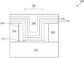
方法100通过在栅极沟槽260中形成围绕DFM的子栅极沟槽300继续到步骤114。DFM在子栅极沟槽300的形成过程中保持完好。在一个实施例中,如图7所示,子栅极沟槽300通过使WF金属堆叠件280在栅极沟槽260中进一步地凹进形成。在另外一个实施例中,子栅极沟槽300通过使WF金属堆叠件280和HK介电层270(未显示)凹进形成。在另外一个实施例中,子栅极沟槽300通过使WF金属堆叠件280,HK介电层270以及侧壁间隔件240(未显示)凹进形成。子栅极沟槽300的深度(d)被控制以达到半导体器件200性能的预定目标。凹进工艺可以被配置以具有相对于DFM 290基本上高的蚀刻选择性。选择性蚀刻包括干蚀刻,湿蚀刻,或干蚀刻与湿蚀刻的组合。借由蚀刻选择性,子栅极沟槽300可以形成为具有自对准特性。或者,子栅极沟槽300也可以通过光刻法和蚀刻工艺形成。
如图8所示,方法100通过在子栅极沟槽300中填充绝缘体保护层310以形成绝缘区315继续到步骤116。绝缘体保护层310包括氧化硅,氮化硅,碳化硅,氮氧化物或者其他合适的材料。绝缘体保护层310被配置为使得在随后的去除DFM 290的蚀刻工艺中获得相对于DFM 290的材料基本上不同的蚀刻速率,这将在下文具体描述。在一个实施例中,如图9所示,CMP工艺被应用,以去除多余的绝缘体保护层310,进而为了随后的蚀刻工艺暴露DFM 290的顶面。As shown in FIG. 8 ,
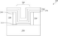
如图10所示,方法100通过完全去除DFM 290以在栅极沟槽260的中心形成MG中心沟槽(MGCT)320继续到步骤118。在一个实施例中,蚀刻工艺被配置从而相对于WF金属堆叠件280和绝缘体保护层310具有基本上高的DFM 290蚀刻选择性。在DFM去除过程中,WF金属堆叠件280和绝缘区315保持相当完好。蚀刻完全去除DFM 290以形成MGCT320。选择性蚀刻包括干蚀刻,湿蚀刻,或干蚀刻与湿蚀刻的组合。借由蚀刻选择性,MGCT沟槽320可以形成为具有自对准特性。在另外一个实施例中,以常规方式的图案化和蚀刻工艺形成MGCT 320。MGCT 320在栅极沟槽260的中间形成,具有由WF金属堆叠件280形成的下部和由绝缘区315形成的上部。As shown in FIG. 10 ,
如图11所示,方法100通过用填充金属330填充MGCT 320继续到步骤120。填充金属330可以包括:铝(Al),铜(Cu)或钨(W),或者其他合适的传导材料。填充金属330通过ALD,PVD,CVD,或者其他合适的工艺沉积。如图11所示,填充金属330和WF金属堆叠件280共同形成MG 350。此外,填充金属330被回蚀到预定高度(h)以获得栅极电阻的调整。在一个实施例中,金属CMP工艺被应用以去除多余的填充金属330,进而为填充金属330,绝缘体保护层310以及ILD层250提供基本上平坦的顶面。因为MG 350的顶面包括隔离区域315的顶面,金属区域的数量在金属CMP工艺中减少,而它导致CMP凹陷降低。MG 350在HK介电层270和IL213上方形成,被称为栅极介电堆叠件。以具有被边缘区域围绕的中心区域的方式形成MG 350。其中,中心区域的上部由填充金属330形成,边缘区域的上部由绝缘区315形成,中心和边缘区域的下部都由WF金属堆叠件形成。As shown in FIG. 11 ,
方法100可以进一步包括通过合适的技术(诸如一次或多次的离子注入)形成源极/漏极(S/D)区域。S/D区域可以进一步包括轻掺杂(LDD)和重掺杂区域。在源极和漏极(S/D)区域形成之后,可以实施一次或更次的退火工艺。退火工艺可以包括快速热退火(RTA),激光退火,或者其他合适的退火工艺。在一个实施例中,S/D区域包括外延生长的半导体材料,从而为适当的应变作用形成应变结构,导致增强载流子迁移率。形成应变结构的方法包括应用蚀刻工艺在半导体衬底210中形成凹槽,并在凹槽中外延生长晶体半导体材料。
方法100也可以进一步包括形成多层互连。多层互连(未显示)可以包括诸如常规通孔或接触件的垂直互连件,和诸如金属线的水平互连件。各种互连部件可以使用各种导电材料,包括铜,钨和硅化物。在一个示例中,使用镶嵌工艺以形成铜相关多层互连结构。在另外一个实施例中,使用钨以在接触孔中形成钨塞。
基于以上,可以看出本发明提供一种IC制造方法,该方法具有填充和去除伪填充材料(DFM)的方案。通过与DFM合作,WF金属堆叠件的形成可以与填充金属的形成分开。这显著地放宽了MG蚀刻中的工艺限制,诸如为了同时满足IC器件性能和MG蚀刻工艺的需求,需要WF金属和填充金属的合适的匹配材料。该方法表现出在MG的形成中极大地降低了金属CMP凹陷和WF金属凹进的失败现象。MG通过该方法形成,该方法可调整填充金属高度和WF金属堆叠件高度,从而满足器件性能的需求。Based on the above, it can be seen that the present invention provides an IC manufacturing method with a scheme for filling and removing dummy fill material (DFM). By working with DFM, the formation of the WF metal stack can be separated from the formation of the fill metal. This significantly relaxes the process constraints in MG etch, such as the need for suitable matching materials of WF metal and fill metal in order to meet both IC device performance and MG etch process demands. This method exhibits greatly reduced metal CMP dishing and WF metal dishing failures in MG formation. The MG is formed by this method, which can adjust the filler metal height and WF metal stack height to meet the needs of device performance.
本发明提供许多不同的制造半导体IC的实施例,其在现有技术之上提供了一种或更多的改进。在一个实施例中,制造半导体集成电路(IC)的方法包括:提供具有栅极沟槽的半导体衬底。该方法还包括:用功函数(WF)金属堆叠件部分填充该栅极沟槽,用伪填充材料(DFM)在该WF金属堆叠件上方填充剩余的栅极沟槽,在该栅极沟槽中形成围绕DFM的子栅极沟槽,用绝缘体保护层填充该子栅极沟槽,以在该栅沟槽中形成绝缘区,随后完全去除该DFM,以在该栅极沟槽中形成MG中心沟槽(MGCT),并用填充金属填充该MGCT。The present invention provides many different embodiments of fabricating semiconductor ICs that provide one or more improvements over the prior art. In one embodiment, a method of fabricating a semiconductor integrated circuit (IC) includes providing a semiconductor substrate having a gate trench. The method also includes partially filling the gate trench with a work function (WF) metal stack, filling the remaining gate trench over the WF metal stack with a dummy fill material (DFM), in the gate trench forming a sub-gate trench surrounding the DFM, filling the sub-gate trench with an insulator capping layer to form an insulating region in the gate trench, and subsequently completely removing the DFM to form an MG center in the gate trench trench (MGCT), and fill the MGCT with a fill metal.
在另外一个实施例中,通过本发明的方法制造的半导体IC包括半导体衬底,在该半导体衬底上形成的栅极介电堆叠件,在该栅极介电堆叠件上方形成的金属栅极(MG)堆叠件;其中,该MG堆叠件具有被边缘区域围绕的中心区域,在该MG堆叠件的中心区域的上部中形成的填充金属,在该MG堆叠件的边缘区域的上部中形成的绝缘区,以及在该MG堆叠件的中心和边缘区域的下部形成的功函数(WF)金属堆叠件。In another embodiment, a semiconductor IC fabricated by the method of the present invention includes a semiconductor substrate, a gate dielectric stack formed on the semiconductor substrate, a metal gate formed over the gate dielectric stack (MG) stack; wherein the MG stack has a central region surrounded by edge regions, a filler metal formed in an upper portion of the central region of the MG stack, a filler metal formed in an upper portion of the edge region of the MG stack An insulating region, and a work function (WF) metal stack formed in the lower portion of the center and edge regions of the MG stack.
在另外一个实施例中,制造半导体集成电路(IC)的方法包括提供半导体衬底,在该半导体衬底上形成伪栅极,在该伪栅极上形成侧壁间隔件,去除该伪栅极以形成栅极沟槽,用功函数(WF)金属堆叠件部分地填充该栅极沟槽,用伪填充材料(DFM)在该WF金属堆叠件上方填充剩余的栅极沟槽,去除WF金属堆叠件的一部分,以在该栅极沟槽中形成具有预定深度(d)的子栅极沟槽,用绝缘体保护层填充该子栅极沟槽,以在该栅极沟槽中形成绝缘区,从该栅极沟槽中完全去除该DFM,以在该栅极沟槽中形成MG中心沟槽(MGCT),并用填充金属填充该MGCT;以及回蚀该填充金属到预定金属高度(h)。In another embodiment, a method of manufacturing a semiconductor integrated circuit (IC) includes providing a semiconductor substrate, forming a dummy gate on the semiconductor substrate, forming a sidewall spacer on the dummy gate, removing the dummy gate To form a gate trench, partially fill the gate trench with a work function (WF) metal stack, fill the remaining gate trench with a dummy fill material (DFM) over the WF metal stack, remove the WF metal stack part of the member to form a sub-gate trench having a predetermined depth (d) in the gate trench, filling the sub-gate trench with an insulator protective layer to form an insulating region in the gate trench, completely removing the DFM from the gate trench to form a MG center trench (MGCT) in the gate trench, filling the MGCT with a fill metal; and etching back the fill metal to a predetermined metal height (h).
上面论述了若干实施例的特征,使得本领域普通技术人员可以更好地理解本发明的各个方面。本领域普通技术人员应该理解,可以很容易地使用本发明作为基础来设计或更改其他用于达到与这里所介绍实施例相同的目的和/或实现相同优点的处理和结构。本领域普通技术人员也应该意识到,这种等效构造并不背离本发明的精神和范围,并且在不背离本发明的精神和范围的情况下,可以进行多种变化、替换以及改变。The above discusses features of several embodiments so that those of ordinary skill in the art may better understand the various aspects of the invention. It should be understood by those skilled in the art that the present invention can be easily used as a basis to design or modify other processes and structures for achieving the same purpose and/or achieving the same advantages as the embodiments presented herein. Those skilled in the art should also realize that such equivalent constructions do not depart from the spirit and scope of the invention, and that they could make various changes, substitutions and alterations herein without departing from the spirit and scope of the invention.
Claims (10)
Applications Claiming Priority (2)
| Application Number | Priority Date | Filing Date | Title |
|---|---|---|---|
| US13/563,470US8507979B1 (en) | 2012-07-31 | 2012-07-31 | Semiconductor integrated circuit with metal gate |
| US13/563,470 | 2012-07-31 |
Publications (2)
| Publication Number | Publication Date |
|---|---|
| CN103578954Atrue CN103578954A (en) | 2014-02-12 |
| CN103578954B CN103578954B (en) | 2016-06-22 |
Family
ID=48916613
Family Applications (1)
| Application Number | Title | Priority Date | Filing Date |
|---|---|---|---|
| CN201210495541.7AActiveCN103578954B (en) | 2012-07-31 | 2012-11-28 | There is the semiconductor integrated circuit of metal gates |
Country Status (4)
| Country | Link |
|---|---|
| US (1) | US8507979B1 (en) |
| KR (1) | KR101396018B1 (en) |
| CN (1) | CN103578954B (en) |
| DE (1) | DE102012111785B4 (en) |
Cited By (7)
| Publication number | Priority date | Publication date | Assignee | Title |
|---|---|---|---|---|
| CN105336589A (en)* | 2014-05-27 | 2016-02-17 | 中芯国际集成电路制造(上海)有限公司 | Formation method of transistor |
| CN106981417A (en)* | 2016-01-19 | 2017-07-25 | 中芯国际集成电路制造(上海)有限公司 | A kind of semiconductor devices and its manufacture method, electronic installation |
| CN107112217A (en)* | 2015-01-08 | 2017-08-29 | 国际商业机器公司 | Metal gates from bottom to top in replacement metal gate finFET device are formed |
| CN107301950A (en)* | 2016-04-14 | 2017-10-27 | 中芯国际集成电路制造(上海)有限公司 | Transistor and forming method thereof |
| CN109786254A (en)* | 2017-11-15 | 2019-05-21 | 台湾积体电路制造股份有限公司 | The high k of selectivity in post tensioned unbonded prestressed concrete technique is formed |
| CN111276543A (en)* | 2014-05-30 | 2020-06-12 | 台湾积体电路制造股份有限公司 | Method of manufacturing semiconductor device |
| US11508583B2 (en) | 2017-11-15 | 2022-11-22 | Taiwan Semiconductor Manufacturing Company, Ltd. | Selective high-k formation in gate-last process |
Families Citing this family (18)
| Publication number | Priority date | Publication date | Assignee | Title |
|---|---|---|---|---|
| CN104681489A (en)* | 2013-11-26 | 2015-06-03 | 中芯国际集成电路制造(上海)有限公司 | Forming method of CMOS (complementary metal-oxide-semiconductor) transistor |
| US9484346B2 (en) | 2014-10-15 | 2016-11-01 | Taiwan Semiconductor Manufacturing Company Ltd | Semiconductor structure and manufacturing method thereof |
| KR102271239B1 (en) | 2015-03-23 | 2021-06-29 | 삼성전자주식회사 | Semiconductor device and method for fabricating the same |
| US9728462B2 (en) | 2015-03-30 | 2017-08-08 | International Business Machines Corporation | Stable multiple threshold voltage devices on replacement metal gate CMOS devices |
| KR102342847B1 (en) | 2015-04-17 | 2021-12-23 | 삼성전자주식회사 | Semiconductor device and manufacturing method of the same |
| US10411113B2 (en) | 2015-05-22 | 2019-09-10 | Taiwan Semiconductor Manufacturing Co., Ltd. | Structure and formation method of semiconductor device structure |
| US9613958B2 (en) | 2015-06-10 | 2017-04-04 | International Business Machines Corporation | Spacer chamfering gate stack scheme |
| KR102474431B1 (en) | 2015-12-08 | 2022-12-06 | 삼성전자주식회사 | Method of manufacturing semiconductor devices |
| KR102497251B1 (en)* | 2015-12-29 | 2023-02-08 | 삼성전자주식회사 | Semiconductor device and method for manufacturing the same |
| US9779997B2 (en)* | 2015-12-31 | 2017-10-03 | Taiwan Semiconductor Manufacturing Co., Ltd. | Semiconductor device and a method for fabricating the same |
| KR102336784B1 (en)* | 2017-06-09 | 2021-12-07 | 삼성전자주식회사 | Semiconductor device |
| US10840205B2 (en) | 2017-09-24 | 2020-11-17 | Invensas Bonding Technologies, Inc. | Chemical mechanical polishing for hybrid bonding |
| KR102692978B1 (en)* | 2017-12-14 | 2024-08-06 | 어플라이드 머티어리얼스, 인코포레이티드 | Methods of etching metal oxides with less etch residue |
| US11056348B2 (en) | 2018-04-05 | 2021-07-06 | Invensas Bonding Technologies, Inc. | Bonding surfaces for microelectronics |
| US10998421B2 (en) | 2018-07-16 | 2021-05-04 | Taiwan Semiconductor Manufacturing Company, Ltd. | Reducing pattern loading in the etch-back of metal gate |
| US11011494B2 (en) | 2018-08-31 | 2021-05-18 | Invensas Bonding Technologies, Inc. | Layer structures for making direct metal-to-metal bonds at low temperatures in microelectronics |
| US11264357B1 (en) | 2020-10-20 | 2022-03-01 | Invensas Corporation | Mixed exposure for large die |
| US12237400B2 (en)* | 2022-04-06 | 2025-02-25 | Taiwan Semiconductor Manufacturing Company, Ltd. | Method of forming semiconductor device |
Family Cites Families (4)
| Publication number | Priority date | Publication date | Assignee | Title |
|---|---|---|---|---|
| DE69534888T2 (en) | 1994-04-06 | 2006-11-02 | Denso Corp., Kariya | Manufacturing method for semiconductor device with trench |
| US8039381B2 (en)* | 2008-09-12 | 2011-10-18 | Taiwan Semiconductor Manufacturing Company, Ltd. | Photoresist etch back method for gate last process |
| US8390058B2 (en)* | 2009-06-12 | 2013-03-05 | Aplha and Omega Semiconductor Incorporated | Configurations and methods for manufacturing devices with trench-oxide-nano-tube super-junctions |
| KR101634748B1 (en)* | 2009-12-08 | 2016-07-11 | 삼성전자주식회사 | method for manufacturing MOS transistor and forming method of integrated circuit using the sime |
- 2012
- 2012-07-31USUS13/563,470patent/US8507979B1/enactiveActive
- 2012-11-28CNCN201210495541.7Apatent/CN103578954B/enactiveActive
- 2012-12-05DEDE102012111785.3Apatent/DE102012111785B4/enactiveActive
- 2012-12-24KRKR1020120152172Apatent/KR101396018B1/enactiveActive
Cited By (12)
| Publication number | Priority date | Publication date | Assignee | Title |
|---|---|---|---|---|
| CN105336589A (en)* | 2014-05-27 | 2016-02-17 | 中芯国际集成电路制造(上海)有限公司 | Formation method of transistor |
| CN105336589B (en)* | 2014-05-27 | 2018-09-07 | 中芯国际集成电路制造(上海)有限公司 | The forming method of transistor |
| CN111276543A (en)* | 2014-05-30 | 2020-06-12 | 台湾积体电路制造股份有限公司 | Method of manufacturing semiconductor device |
| CN111276543B (en)* | 2014-05-30 | 2024-01-30 | 台湾积体电路制造股份有限公司 | Method for manufacturing semiconductor device |
| CN107112217A (en)* | 2015-01-08 | 2017-08-29 | 国际商业机器公司 | Metal gates from bottom to top in replacement metal gate finFET device are formed |
| CN106981417A (en)* | 2016-01-19 | 2017-07-25 | 中芯国际集成电路制造(上海)有限公司 | A kind of semiconductor devices and its manufacture method, electronic installation |
| CN106981417B (en)* | 2016-01-19 | 2020-03-06 | 中芯国际集成电路制造(上海)有限公司 | A kind of semiconductor device and its manufacturing method, electronic device |
| CN107301950A (en)* | 2016-04-14 | 2017-10-27 | 中芯国际集成电路制造(上海)有限公司 | Transistor and forming method thereof |
| US11295955B2 (en) | 2016-04-14 | 2022-04-05 | Semiconductor Manufacturing International (Shanghai) Corporation | Transistor |
| CN109786254A (en)* | 2017-11-15 | 2019-05-21 | 台湾积体电路制造股份有限公司 | The high k of selectivity in post tensioned unbonded prestressed concrete technique is formed |
| CN109786254B (en)* | 2017-11-15 | 2022-03-22 | 台湾积体电路制造股份有限公司 | Selective high-k formation in gate last process |
| US11508583B2 (en) | 2017-11-15 | 2022-11-22 | Taiwan Semiconductor Manufacturing Company, Ltd. | Selective high-k formation in gate-last process |
Also Published As
| Publication number | Publication date |
|---|---|
| DE102012111785B4 (en) | 2014-10-02 |
| US8507979B1 (en) | 2013-08-13 |
| CN103578954B (en) | 2016-06-22 |
| KR20140016792A (en) | 2014-02-10 |
| DE102012111785A1 (en) | 2014-02-06 |
| KR101396018B1 (en) | 2014-05-16 |
Similar Documents
| Publication | Publication Date | Title |
|---|---|---|
| CN103578954B (en) | There is the semiconductor integrated circuit of metal gates | |
| US10431473B2 (en) | FINFET with source/drain structure and method of fabrication thereof | |
| US20220336632A1 (en) | Gate Patterning Process For Multi-Gate Devices | |
| US8609495B2 (en) | Hybrid gate process for fabricating finfet device | |
| CN103811550B (en) | The contact structures of semiconductor device | |
| TWI718311B (en) | Method of fabricating fin-like field effect transistor | |
| US12159924B2 (en) | Structure and method for multigate devices with suppressed diffusion | |
| US20210391447A1 (en) | Inner Spacer Formation in Multi-Gate Transistors | |
| US10062769B2 (en) | Methods of fabricating semiconductor devices | |
| KR20130027982A (en) | Improved silicide formation and associated devices | |
| KR101419122B1 (en) | Method of semiconductor integrated circuit fabrication | |
| TWI728481B (en) | Semiconductor structures and methods of forming the same | |
| US10062780B2 (en) | FinFET device | |
| US11282705B2 (en) | Semiconductor device and method of forming the same | |
| US10497628B2 (en) | Methods of forming epitaxial structures in fin-like field effect transistors | |
| CN103811538B (en) | With device income and the improved metal gate structure of productivity ratio | |
| CN103578953B (en) | The method that semiconductor integrated circuit manufactures | |
| CN113270364A (en) | Method for manufacturing semiconductor device |
Legal Events
| Date | Code | Title | Description |
|---|---|---|---|
| C06 | Publication | ||
| PB01 | Publication | ||
| SE01 | Entry into force of request for substantive examination | ||
| SE01 | Entry into force of request for substantive examination | ||
| C14 | Grant of patent or utility model | ||
| GR01 | Patent grant | ||
| TR01 | Transfer of patent right | Effective date of registration:20250127 Address after:texas Patentee after:Palabelen Strategic Opportunities Fund LLC Country or region after:U.S.A. Address before:China Taiwan Patentee before:Taiwan Semiconductor Manufacturing Co.,Ltd. Country or region before:TaiWan, China | |
| TR01 | Transfer of patent right |