CN103560147A - Nitrogen and phosphorus zinc oxide thin film, preparation method thereof and thin film transistor - Google Patents
Nitrogen and phosphorus zinc oxide thin film, preparation method thereof and thin film transistorDownload PDFInfo
- Publication number
- CN103560147A CN103560147ACN201310554881.7ACN201310554881ACN103560147ACN 103560147 ACN103560147 ACN 103560147ACN 201310554881 ACN201310554881 ACN 201310554881ACN 103560147 ACN103560147 ACN 103560147A
- Authority
- CN
- China
- Prior art keywords
- nitrogen
- nitrogen phosphorus
- sputtering
- phosphorus oxygen
- thin film
- Prior art date
- Legal status (The legal status is an assumption and is not a legal conclusion. Google has not performed a legal analysis and makes no representation as to the accuracy of the status listed.)
- Granted
Links
- IJGRMHOSHXDMSA-UHFFFAOYSA-NAtomic nitrogenChemical compoundN#NIJGRMHOSHXDMSA-UHFFFAOYSA-N0.000titleclaimsabstractdescription78
- 229910052757nitrogenInorganic materials0.000titleclaimsabstractdescription36
- 239000010409thin filmSubstances0.000titleclaimsabstractdescription36
- 238000002360preparation methodMethods0.000titleclaimsabstractdescription7
- DLISVLVFJRCVJM-UHFFFAOYSA-Nzinc oxygen(2-) phosphaneChemical compound[O--].P.[Zn++]DLISVLVFJRCVJM-UHFFFAOYSA-N0.000title1
- 238000004544sputter depositionMethods0.000claimsabstractdescription35
- OAICVXFJPJFONN-UHFFFAOYSA-NPhosphorusChemical compound[P]OAICVXFJPJFONN-UHFFFAOYSA-N0.000claimsabstractdescription29
- 239000011574phosphorusSubstances0.000claimsabstractdescription29
- 229910052698phosphorusInorganic materials0.000claimsabstractdescription28
- IPDZGBLBEDHVOD-UHFFFAOYSA-N[Zn].[P].[O].[N]Chemical compound[Zn].[P].[O].[N]IPDZGBLBEDHVOD-UHFFFAOYSA-N0.000claimsabstractdescription19
- 239000000463materialSubstances0.000claimsabstractdescription9
- 239000010408filmSubstances0.000claimsdescription38
- 239000011701zincSubstances0.000claimsdescription34
- 239000001301oxygenSubstances0.000claimsdescription27
- 229910052760oxygenInorganic materials0.000claimsdescription27
- QVGXLLKOCUKJST-UHFFFAOYSA-Natomic oxygenChemical compound[O]QVGXLLKOCUKJST-UHFFFAOYSA-N0.000claimsdescription25
- 239000000758substrateSubstances0.000claimsdescription22
- 239000004065semiconductorSubstances0.000claimsdescription20
- 239000007789gasSubstances0.000claimsdescription18
- HCHKCACWOHOZIP-UHFFFAOYSA-NZincChemical compound[Zn]HCHKCACWOHOZIP-UHFFFAOYSA-N0.000claimsdescription17
- 229910052725zincInorganic materials0.000claimsdescription16
- 238000001755magnetron sputter depositionMethods0.000claimsdescription12
- XKRFYHLGVUSROY-UHFFFAOYSA-NArgonChemical compound[Ar]XKRFYHLGVUSROY-UHFFFAOYSA-N0.000claimsdescription10
- 238000004519manufacturing processMethods0.000claimsdescription7
- 238000000576coating methodMethods0.000claimsdescription6
- 229910052786argonInorganic materials0.000claimsdescription5
- 239000011248coating agentSubstances0.000claimsdescription5
- 238000005530etchingMethods0.000claimsdescription3
- 229910001873dinitrogenInorganic materials0.000claimsdescription2
- 239000013077target materialSubstances0.000claimsdescription2
- 239000012212insulatorSubstances0.000claims3
- 238000002156mixingMethods0.000claims2
- 230000001105regulatory effectEffects0.000claims2
- 230000004888barrier functionEffects0.000claims1
- 238000005477sputtering targetMethods0.000claims1
- 239000000203mixtureSubstances0.000abstractdescription8
- 239000010410layerSubstances0.000description29
- XLOMVQKBTHCTTD-UHFFFAOYSA-NZinc monoxideChemical compound[Zn]=OXLOMVQKBTHCTTD-UHFFFAOYSA-N0.000description24
- 239000011787zinc oxideSubstances0.000description11
- 238000000034methodMethods0.000description10
- 238000012360testing methodMethods0.000description7
- XUIMIQQOPSSXEZ-UHFFFAOYSA-NSiliconChemical compound[Si]XUIMIQQOPSSXEZ-UHFFFAOYSA-N0.000description5
- 230000007547defectEffects0.000description5
- 229910052710siliconInorganic materials0.000description5
- 239000010703siliconSubstances0.000description5
- 230000005355Hall effectEffects0.000description4
- 230000008901benefitEffects0.000description4
- 230000007423decreaseEffects0.000description4
- 238000000151depositionMethods0.000description4
- 238000005516engineering processMethods0.000description4
- 230000005669field effectEffects0.000description4
- 229910052751metalInorganic materials0.000description4
- 239000002184metalSubstances0.000description4
- -1oxygen anionsChemical class0.000description4
- 230000008569processEffects0.000description4
- 238000005566electron beam evaporationMethods0.000description3
- 238000001941electron spectroscopyMethods0.000description3
- 230000009643growth defectEffects0.000description3
- 239000004973liquid crystal related substanceSubstances0.000description3
- RTAQQCXQSZGOHL-UHFFFAOYSA-NTitaniumChemical group[Ti]RTAQQCXQSZGOHL-UHFFFAOYSA-N0.000description2
- 150000001768cationsChemical class0.000description2
- 239000004020conductorSubstances0.000description2
- 238000011161developmentMethods0.000description2
- 238000009826distributionMethods0.000description2
- 150000002500ionsChemical class0.000description2
- 238000002207thermal evaporationMethods0.000description2
- 229910052719titaniumInorganic materials0.000description2
- 239000010936titaniumSubstances0.000description2
- 229920001621AMOLEDPolymers0.000description1
- VYZAMTAEIAYCRO-UHFFFAOYSA-NChromiumChemical compound[Cr]VYZAMTAEIAYCRO-UHFFFAOYSA-N0.000description1
- RYGMFSIKBFXOCR-UHFFFAOYSA-NCopperChemical compound[Cu]RYGMFSIKBFXOCR-UHFFFAOYSA-N0.000description1
- MYMOFIZGZYHOMD-UHFFFAOYSA-NDioxygenChemical compoundO=OMYMOFIZGZYHOMD-UHFFFAOYSA-N0.000description1
- ZOKXTWBITQBERF-UHFFFAOYSA-NMolybdenumChemical compound[Mo]ZOKXTWBITQBERF-UHFFFAOYSA-N0.000description1
- 229910052581Si3N4Inorganic materials0.000description1
- 229910004205SiNXInorganic materials0.000description1
- 229910004298SiO 2Inorganic materials0.000description1
- BQCADISMDOOEFD-UHFFFAOYSA-NSilverChemical compound[Ag]BQCADISMDOOEFD-UHFFFAOYSA-N0.000description1
- SJWUULVPYAMRCJ-UHFFFAOYSA-N[N].[O].[P]Chemical compound[N].[O].[P]SJWUULVPYAMRCJ-UHFFFAOYSA-N0.000description1
- YUWBVKYVJWNVLE-UHFFFAOYSA-N[N].[P]Chemical compound[N].[P]YUWBVKYVJWNVLE-UHFFFAOYSA-N0.000description1
- 239000000956alloySubstances0.000description1
- 229910045601alloyInorganic materials0.000description1
- 229910052782aluminiumInorganic materials0.000description1
- XAGFODPZIPBFFR-UHFFFAOYSA-NaluminiumChemical compound[Al]XAGFODPZIPBFFR-UHFFFAOYSA-N0.000description1
- 229910021417amorphous siliconInorganic materials0.000description1
- 150000001450anionsChemical class0.000description1
- 238000000231atomic layer depositionMethods0.000description1
- 239000011230binding agentSubstances0.000description1
- 230000015572biosynthetic processEffects0.000description1
- 229910052804chromiumInorganic materials0.000description1
- 239000011651chromiumSubstances0.000description1
- 238000011109contaminationMethods0.000description1
- 229910052802copperInorganic materials0.000description1
- 239000010949copperSubstances0.000description1
- RKTYLMNFRDHKIL-UHFFFAOYSA-Ncopper;5,10,15,20-tetraphenylporphyrin-22,24-diideChemical compound[Cu+2].C1=CC(C(=C2C=CC([N-]2)=C(C=2C=CC=CC=2)C=2C=CC(N=2)=C(C=2C=CC=CC=2)C2=CC=C3[N-]2)C=2C=CC=CC=2)=NC1=C3C1=CC=CC=C1RKTYLMNFRDHKIL-UHFFFAOYSA-N0.000description1
- 230000007812deficiencyEffects0.000description1
- 230000008021depositionEffects0.000description1
- 238000010586diagramMethods0.000description1
- 230000005611electricityEffects0.000description1
- 230000007613environmental effectEffects0.000description1
- 238000002474experimental methodMethods0.000description1
- 239000011521glassSubstances0.000description1
- PCHJSUWPFVWCPO-UHFFFAOYSA-NgoldChemical compound[Au]PCHJSUWPFVWCPO-UHFFFAOYSA-N0.000description1
- 229910052737goldInorganic materials0.000description1
- 239000010931goldSubstances0.000description1
- 230000006872improvementEffects0.000description1
- 239000011159matrix materialSubstances0.000description1
- 230000007246mechanismEffects0.000description1
- 229910044991metal oxideInorganic materials0.000description1
- 150000004706metal oxidesChemical class0.000description1
- 238000012986modificationMethods0.000description1
- 230000004048modificationEffects0.000description1
- 229910052750molybdenumInorganic materials0.000description1
- 239000011733molybdenumSubstances0.000description1
- MWUXSHHQAYIFBG-UHFFFAOYSA-Nnitrogen oxideInorganic materialsO=[N]MWUXSHHQAYIFBG-UHFFFAOYSA-N0.000description1
- TWNQGVIAIRXVLR-UHFFFAOYSA-Noxo(oxoalumanyloxy)alumaneChemical compoundO=[Al]O[Al]=OTWNQGVIAIRXVLR-UHFFFAOYSA-N0.000description1
- SIWVEOZUMHYXCS-UHFFFAOYSA-Noxo(oxoyttriooxy)yttriumChemical compoundO=[Y]O[Y]=OSIWVEOZUMHYXCS-UHFFFAOYSA-N0.000description1
- 229910001392phosphorus oxideInorganic materials0.000description1
- 238000000623plasma-assisted chemical vapour depositionMethods0.000description1
- 229910021420polycrystalline siliconInorganic materials0.000description1
- 229920005591polysiliconPolymers0.000description1
- 238000005036potential barrierMethods0.000description1
- 239000000843powderSubstances0.000description1
- 238000004549pulsed laser depositionMethods0.000description1
- 239000010453quartzSubstances0.000description1
- 230000004044responseEffects0.000description1
- VYPSYNLAJGMNEJ-UHFFFAOYSA-Nsilicon dioxideInorganic materialsO=[Si]=OVYPSYNLAJGMNEJ-UHFFFAOYSA-N0.000description1
- HQVNEWCFYHHQES-UHFFFAOYSA-Nsilicon nitrideChemical compoundN12[Si]34N5[Si]62N3[Si]51N64HQVNEWCFYHHQES-UHFFFAOYSA-N0.000description1
- 229910052814silicon oxideInorganic materials0.000description1
- 239000002210silicon-based materialSubstances0.000description1
- 229910052709silverInorganic materials0.000description1
- 239000004332silverSubstances0.000description1
- 239000002356single layerSubstances0.000description1
- 238000005507sprayingMethods0.000description1
- 238000006467substitution reactionMethods0.000description1
- 229910052715tantalumInorganic materials0.000description1
- GUVRBAGPIYLISA-UHFFFAOYSA-Ntantalum atomChemical compound[Ta]GUVRBAGPIYLISA-UHFFFAOYSA-N0.000description1
- WFKWXMTUELFFGS-UHFFFAOYSA-NtungstenChemical compound[W]WFKWXMTUELFFGS-UHFFFAOYSA-N0.000description1
- 229910052721tungstenInorganic materials0.000description1
- 239000010937tungstenSubstances0.000description1
Images
Classifications
- H—ELECTRICITY
- H10—SEMICONDUCTOR DEVICES; ELECTRIC SOLID-STATE DEVICES NOT OTHERWISE PROVIDED FOR
- H10D—INORGANIC ELECTRIC SEMICONDUCTOR DEVICES
- H10D62/00—Semiconductor bodies, or regions thereof, of devices having potential barriers
- H10D62/80—Semiconductor bodies, or regions thereof, of devices having potential barriers characterised by the materials
- C—CHEMISTRY; METALLURGY
- C23—COATING METALLIC MATERIAL; COATING MATERIAL WITH METALLIC MATERIAL; CHEMICAL SURFACE TREATMENT; DIFFUSION TREATMENT OF METALLIC MATERIAL; COATING BY VACUUM EVAPORATION, BY SPUTTERING, BY ION IMPLANTATION OR BY CHEMICAL VAPOUR DEPOSITION, IN GENERAL; INHIBITING CORROSION OF METALLIC MATERIAL OR INCRUSTATION IN GENERAL
- C23C—COATING METALLIC MATERIAL; COATING MATERIAL WITH METALLIC MATERIAL; SURFACE TREATMENT OF METALLIC MATERIAL BY DIFFUSION INTO THE SURFACE, BY CHEMICAL CONVERSION OR SUBSTITUTION; COATING BY VACUUM EVAPORATION, BY SPUTTERING, BY ION IMPLANTATION OR BY CHEMICAL VAPOUR DEPOSITION, IN GENERAL
- C23C14/00—Coating by vacuum evaporation, by sputtering or by ion implantation of the coating forming material
- C23C14/22—Coating by vacuum evaporation, by sputtering or by ion implantation of the coating forming material characterised by the process of coating
- C23C14/34—Sputtering
- C23C14/3464—Sputtering using more than one target
- H—ELECTRICITY
- H01—ELECTRIC ELEMENTS
- H01L—SEMICONDUCTOR DEVICES NOT COVERED BY CLASS H10
- H01L21/00—Processes or apparatus adapted for the manufacture or treatment of semiconductor or solid state devices or of parts thereof
- H01L21/02—Manufacture or treatment of semiconductor devices or of parts thereof
- H01L21/02104—Forming layers
- H01L21/02365—Forming inorganic semiconducting materials on a substrate
- H01L21/02612—Formation types
- H01L21/02617—Deposition types
- H01L21/02631—Physical deposition at reduced pressure, e.g. MBE, sputtering, evaporation
- H—ELECTRICITY
- H10—SEMICONDUCTOR DEVICES; ELECTRIC SOLID-STATE DEVICES NOT OTHERWISE PROVIDED FOR
- H10D—INORGANIC ELECTRIC SEMICONDUCTOR DEVICES
- H10D30/00—Field-effect transistors [FET]
- H10D30/01—Manufacture or treatment
- H10D30/021—Manufacture or treatment of FETs having insulated gates [IGFET]
- H10D30/031—Manufacture or treatment of FETs having insulated gates [IGFET] of thin-film transistors [TFT]
Landscapes
- Engineering & Computer Science (AREA)
- Chemical & Material Sciences (AREA)
- Organic Chemistry (AREA)
- Materials Engineering (AREA)
- Mechanical Engineering (AREA)
- Metallurgy (AREA)
- Chemical Kinetics & Catalysis (AREA)
- Physics & Mathematics (AREA)
- Condensed Matter Physics & Semiconductors (AREA)
- General Physics & Mathematics (AREA)
- Manufacturing & Machinery (AREA)
- Computer Hardware Design (AREA)
- Microelectronics & Electronic Packaging (AREA)
- Power Engineering (AREA)
- Thin Film Transistor (AREA)
Abstract
Translated fromChinese
Description
Translated fromChinese技术领域technical field
本发明涉及一种半导体薄膜的制备,特别是涉及一种氮磷氧锌薄膜及其制备方法和薄膜晶体管。The invention relates to the preparation of a semiconductor thin film, in particular to a nitrogen, phosphorus, oxygen and zinc thin film, a preparation method thereof and a thin film transistor.
背景技术Background technique
在近十几年的时间中,以硅材料TFT为驱动单元的液晶显示器件以其体积小、重量轻、品质高等一系列优点获得了迅速发展,并成为主流的信息显示终端。然而随着人们对显示器件分辨率、响应速度、稳定性等性能要求的提高,以硅材料为有源层的TFT暴露出一系列的问题,a-Si TFT背板由于其自身迁移率较低(一般小于0.5cm2/(V·s),无法实现高分辨率显示;低温多晶硅(LTPS)TFT技术生产工艺复杂,设备投资高,面板面临均匀性差、良品率低、生产成本居高不下等难以克服的问题,其在大尺寸FPD显示领域的进一步发展受到较大限制。In the past ten years, the liquid crystal display device with silicon TFT as the driving unit has achieved rapid development due to its advantages of small size, light weight and high quality, and has become the mainstream information display terminal. However, with the improvement of people's performance requirements for display device resolution, response speed, and stability, TFTs with silicon materials as the active layer have exposed a series of problems. (Generally less than 0.5cm2 /(V s), high-resolution display cannot be realized; low-temperature polysilicon (LTPS) TFT technology has complex production process, high equipment investment, poor panel uniformity, low yield rate, high production cost, etc. It is an insurmountable problem, and its further development in the field of large-size FPD display is greatly restricted.
与目前在液晶显示器有源驱动矩阵中广泛采用的硅TFT相比,氧化物半导体TFT具有如下优势:(1)场效应迁移率较高;(2)开关比高;(3)制备工艺温度低;(4)可以制作大面积非晶薄膜,均匀性好,具有良好一致的电学特性;(5)受可见光影响小,比非晶硅薄膜晶体管稳定;(6)可以制作成透明器件。在平板显示领域,氧化物TFT技术几乎满足包括AMOLED驱动、快速超大屏幕液晶显示、3D显示等诸多显示模式的所有要求。在柔性显示方面,衬底材料不能承受高温,而氧化物TFT的制备工艺温度低,与柔性衬底兼容,因而金属氧化物TFT具备较大优势。Compared with silicon TFTs widely used in the active drive matrix of liquid crystal displays, oxide semiconductor TFTs have the following advantages: (1) higher field-effect mobility; (2) high switching ratio; (3) low manufacturing process temperature ; (4) Large-area amorphous thin films can be produced, with good uniformity and good and consistent electrical properties; (5) Less affected by visible light, more stable than amorphous silicon thin film transistors; (6) Can be made into transparent devices. In the field of flat panel display, oxide TFT technology almost meets all the requirements of many display modes including AMOLED drive, fast ultra-large-screen liquid crystal display, 3D display and so on. In terms of flexible display, the substrate material cannot withstand high temperatures, and the fabrication process temperature of oxide TFT is low, which is compatible with flexible substrates, so metal oxide TFT has great advantages.
但在典型的a-IGZO中,大量正离子的随机分布了形成电子的散射机构,导致载流子迁移率相对较低。且由于在a-IGZO薄膜中存在大量氧空位,在光照和负偏压的条件下,其带隙中施主型氧空位的存在将会导致器件的稳定性变差,因此该薄膜晶体管存在稳定性问题。But in typical a-IGZO, the random distribution of a large number of positive ions creates a scattering mechanism for electrons, resulting in relatively low carrier mobility. And because there are a large number of oxygen vacancies in the a-IGZO thin film, under the conditions of light and negative bias, the existence of donor oxygen vacancies in its band gap will lead to poor stability of the device, so the thin film transistor has a stable question.
发明内容Contents of the invention
本发明所要解决的技术问题是:弥补上述现有技术的不足,提出一种氮磷氧锌薄膜及其制备方法和薄膜晶体管,其制作的薄膜晶体管能获得最大载流子迁移率The technical problem to be solved by the present invention is to make up for the deficiencies of the above-mentioned prior art, and propose a nitrogen, phosphorus, oxyzinc thin film and its preparation method and a thin film transistor, and the thin film transistor produced by it can obtain the maximum carrier mobility
本发明的技术问题通过以下的技术方案予以解决:Technical problem of the present invention is solved by following technical scheme:
一种氮磷氧锌薄膜,其组成为ZnxPyO1-x-y-zNz,其中,55%≤x≤65%,1%≤y≤10%,10%≤z≤22%,各原子的原子个数百分比之和为100%。A nitrogen phosphorus oxyzinc thin film, its composition is Znx Py O1-xyz Nz , wherein, 55%≤x≤65%, 1%≤y≤10%, 10%≤z≤22%, each atom The sum of the atomic number percentages is 100%.
优选地,59%≤x≤61%,5%≤y≤8%,12%≤z≤15%。Preferably, 59%≤x≤61%, 5%≤y≤8%, 12%≤z≤15%.
本发明采用非氧的阴离子代替氧化锌中氧离子,进而调整氧化物的价带,消除氧化物半导体中的氧空位,且由于阳离子几乎都是Zn2+,不同于传统的a-IGZO中,存在大量阳离子的随机分布,降低了载流子传输中的势垒。实验表明:The present invention uses non-oxygen anions to replace oxygen ions in zinc oxide, thereby adjusting the valence band of the oxide and eliminating oxygen vacancies in the oxide semiconductor, and because the cations are almost all Zn2+ , which is different from the traditional a-IGZO, There is a random distribution of a large number of cations, lowering the potential barrier in carrier transport. Experiments show that:
含锌的半导体本质上是靠阴离子缺位(缺陷)导电,如果锌含量少了,导电能力降低,如果锌含量过高,说明存在大量缺陷,越来越接近导体,性能好的TFT用薄膜需要在这之间找到平衡,获得导电能力适当,缺陷不太多,本发明中当原子锌小于55%时,薄膜的载流子迁移率降低,当原子锌大于65%时,薄膜呈多晶结构且具有大量生长缺陷。Zinc-containing semiconductors essentially rely on anion vacancies (defects) to conduct electricity. If the zinc content is small, the conductivity will decrease. If the zinc content is too high, it means that there are a large number of defects, and it is getting closer to the conductor. TFT films with good performance need Find a balance between these, obtain appropriate electrical conductivity, and not too many defects. In the present invention, when the atomic zinc is less than 55%, the carrier mobility of the film decreases. When the atomic zinc is greater than 65%, the film is a polycrystalline structure. And has a large number of growth defects.
在溅射过程中,立方形Zn3N2、六角形ZnO和属于四方晶系的Zn3P2间存在生长竞争关系,有助于氮氧磷锌非晶相的形成,然而当氮、磷含量减小时,薄膜呈现ZnO的多晶结构,当氧气含量减小时,薄膜呈现Zn3N2或Zn3P2的多晶结构。所以,当原子磷小于1%时,薄膜容易形成多晶结构,薄膜的缺陷多,当原子磷大于10%时,薄膜呈多晶结构且具有大量生长缺陷,相应的薄膜晶体管漏电流大;当原子氮小于10%时,薄膜容易形成多晶结构,薄膜的缺陷多,当原子氮大于22%时,薄膜呈多晶结构且具有大量生长缺陷,相应的薄膜晶体管漏电流大。During the sputtering process, there is a growth competition relationship between cubic Zn3 N2 , hexagonal ZnO and tetragonal Zn3 P2 , which contributes to the formation of nitrogen oxide phosphorus zinc amorphous phase. However, when nitrogen, phosphorus When the oxygen content decreases, the film presents the polycrystalline structure of ZnO, and when the oxygen content decreases, the film presents the polycrystalline structure of Zn3 N2 or Zn3 P2 . Therefore, when the atomic phosphorus is less than 1%, the film is easy to form a polycrystalline structure and has many defects; when the atomic phosphorus is greater than 10%, the film has a polycrystalline structure and a large number of growth defects, and the corresponding thin film transistor leakage current is large; When the atomic nitrogen is less than 10%, the film is easy to form a polycrystalline structure and has many defects. When the atomic nitrogen is greater than 22%, the film has a polycrystalline structure and a large number of growth defects, and the corresponding thin film transistor leakage current is large.
本发明中的氮磷氧锌薄膜呈非晶态,其表面平整,采用Accent HL5500PC型Hall效应测试系统测试载流子浓度和Hall迁移率。优化条件下的载流子浓度较低~1017cm-3,Hall迁移率达到49cm2/Vs。The nitrogen, phosphorus, oxyzinc thin film in the present invention is in an amorphous state, and its surface is smooth. The Accent HL5500PC Hall effect test system is used to test the carrier concentration and Hall mobility. Under optimized conditions, the carrier concentration is as low as ~1017 cm-3 , and the Hall mobility reaches 49cm2 /Vs.
本发明的另一个目的是在反应性气氛中通过磁控溅射来制造氮磷氧锌薄膜的方法,反应性气氛由纯氧气或纯氮气或者二者的任意混合或者二者与氩气的任意混合构成,如氮气/氩气的混合物,氧气/氮气/氩气的混合物,氧气/氮气的混合物所构成,所述的溅射镀膜的方法可以使将不同材料制作成靶材并安装在不同的靶位上同时溅射,通过调节不同靶位的溅射功率来控制所制备薄膜中各原子的比例;或者将其中的两种材料按照所述原子比例制作成一个靶材,然后再与其它靶材安装在不同靶位上实施共溅射,通过调节不同靶位的溅射功率来控制所制备薄膜中各原子的比例。Another object of the present invention is a method for manufacturing nitrogen, phosphorus, oxygen and zinc films by magnetron sputtering in a reactive atmosphere, the reactive atmosphere is composed of pure oxygen or pure nitrogen or any mixture of the two or any combination of the two and argon. Mixed composition, such as a mixture of nitrogen/argon, a mixture of oxygen/nitrogen/argon, and a mixture of oxygen/nitrogen, the sputtering coating method can make different materials into targets and install them on different Simultaneous sputtering on the target position, the ratio of each atom in the prepared film is controlled by adjusting the sputtering power of different target positions; or the two materials are made into a target according to the atomic ratio, and then combined with other targets The material is installed on different target positions for co-sputtering, and the ratio of each atom in the prepared film is controlled by adjusting the sputtering power of different target positions.
所述靶材为ZnO靶、P2O5靶、Zn3N2靶或Zn3P2靶。The target material is a ZnO target, a P2 O5 target, a Zn3 N2 target or a Zn3 P2 target.
采用射频磁控溅射,靶与衬底的距离为20-150mm,所用的射频频率13.56MHz,反应性气氛的各种气体的比例通过气体流量计控制。样品生长时衬底温度保持在25-100℃以内,在0.5W/cm2-5W/cm2的功率密度下实施溅射,溅射室的背景真空小于1×10-7托,溅射压强控制在0.1Pa-10.0Pa间。Using radio frequency magnetron sputtering, the distance between the target and the substrate is 20-150 mm, the radio frequency used is 13.56 MHz, and the ratio of various gases in the reactive atmosphere is controlled by a gas flow meter. When the sample grows, the substrate temperature is kept within 25-100°C, sputtering is performed at a power density of 0.5W/cm2 -5W/cm2 , the background vacuum of the sputtering chamber is less than 1×10⁻⁷ Torr, and the sputtering pressure Control between 0.1Pa-10.0Pa.
一种采用顶栅结构的薄膜晶体管,包括基板,形成在基板上的源极、漏极和氮磷氧锌半导体有源层,栅极和栅极绝缘层;所述源极和漏极分别与所述氮磷氧锌半导体有源层接触,所述栅极绝缘层覆盖在所述氮磷氧锌半导体有源层上、以及所述栅极形成在所述栅极绝缘层上,沟道区域位于所述源极和漏极之间,所述栅极与绝缘层以及沟道区域形成自对准,所述氮磷氧锌半导体有源层由上述的氮磷氧锌薄膜刻蚀形成。A thin-film transistor adopting a top-gate structure, comprising a substrate, a source electrode, a drain electrode, and a nitrogen, phosphorus, oxide and zinc semiconductor active layer formed on the substrate, a gate electrode and a gate insulating layer; the source electrode and the drain electrode are respectively connected to the The nitrogen-phosphorus-oxygen-zinc semiconductor active layer contacts, the gate insulating layer covers the nitrogen-phosphorus-oxygen-zinc semiconductor active layer, and the gate is formed on the gate insulating layer, and the channel region Located between the source electrode and the drain electrode, the gate is self-aligned with the insulating layer and the channel region, and the nitrogen, phosphorus, oxygen and zinc semiconductor active layer is formed by etching the above nitrogen, phosphorus, and oxygen zinc film.
该结构的优势在于氮磷氧锌半导体有源层被栅极绝缘层覆盖,不会受环境或工艺因素的影响且没有增加额外的工艺处理步骤。The advantage of this structure is that the nitrogen, phosphorus, oxygen and zinc semiconductor active layer is covered by the gate insulating layer, which is not affected by environmental or process factors and does not add additional process steps.
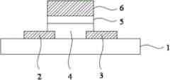
附图说明Description of drawings
图1为实例中所制备的氮磷氧锌薄膜晶体管的结构图。FIG. 1 is a structure diagram of a nitrogen, phosphorus, and oxygen zinc thin film transistor prepared in an example.
具体实施方式Detailed ways
下面对照附图并结合优选的实施方式对本发明作进一步说明。The present invention will be further described below with reference to the accompanying drawings and in combination with preferred embodiments.
本发明在氧化锌材料中同时掺磷和氮,其组成为ZnxPyO1-x-y-zNz,其中,55%≤x≤65%,1%≤y≤10%,10%≤z≤22%。并通过离子溅射沉积该氮磷氧锌薄膜,同时对于给定薄膜材料制作的薄膜晶体管获得高载流子迁移率和高稳定性。In the present invention, zinc oxide material is doped with phosphorus and nitrogen at the same time, and its composition is Znx Py O1-xyz Nz , wherein, 55%≤x≤65%, 1%≤y≤10%, 10%≤z≤ twenty two%. And the nitrogen, phosphorus, oxyzinc thin film is deposited by ion sputtering, and at the same time, high carrier mobility and high stability are obtained for a thin film transistor made of a given thin film material.
实施例1Example 1
将ZnO靶、P2O5靶和Zn3N2分别安装在三个不同靶位同时溅射,通过调节不同靶位的溅射功率控制镀膜速度,使ZnO、P2O5和ZnN的溅射镀膜速度比为1:1:12,相应的原子比约为Zn:P:N=13:2:12。The ZnO target, P2 O5 target and Zn3 N2 were respectively installed in three different target positions for simultaneous sputtering, and the coating speed was controlled by adjusting the sputtering power of different target positions, so that the sputtering of ZnO, P2 O5 and ZnN The spray coating speed ratio is 1:1:12, and the corresponding atomic ratio is about Zn:P:N=13:2:12.
ZnOPN采用射频磁控溅射,靶与衬底的距离为60mm,所用的射频频率13.56MHz,以高纯氮气和氧气的混合气体为溅射气体(反应性气氛),气体的比例通过气体流量计控制。溅射室的背景真空小于1×10⁻⁷托,为了防止污染,首先进行预溅射10min,样品生长时衬底温度保持在室温25℃,氧流量为5sccm,氮流量为20sccm。在0.8Pa压力和2W/cm2的功率密度下完成溅射镀膜。ZnOPN adopts radio frequency magnetron sputtering, the distance between the target and the substrate is 60mm, the radio frequency used is 13.56MHz, and the mixed gas of high-purity nitrogen and oxygen is used as the sputtering gas (reactive atmosphere), and the gas ratio is passed through the gas flow meter control. The background vacuum of the sputtering chamber was less than 1×10⁻⁷ Torr. In order to prevent contamination, pre-sputtering was carried out for 10 minutes. The substrate temperature was kept at room temperature 25°C during sample growth, and the flow rate of oxygen was 5 sccm, and the flow rate of nitrogen was 20 sccm. The sputter coating was done under the pressure of 0.8Pa and the power density of 2W/cm2 .
所制备的氮磷氧锌薄膜的元素含量由X射线电子能谱(XPS)测定,其中锌含量为59%,磷含量为6%,氮含量为14%,氧含量为21%。The element content of the prepared nitrogen, phosphorus, and oxyzinc films was determined by X-ray electron spectroscopy (XPS), and the zinc content was 59%, the phosphorus content was 6%, the nitrogen content was 14%, and the oxygen content was 21%.
采用Accent HL 5500PC型Hall效应测试系统测试薄膜载流子浓度和Hall迁移率,载流子浓度较低~1017cm-3,Hall迁移率为30cm2/Vs。薄膜呈非晶态。开关比达到107。Accent HL 5500PC Hall Effect Test System was used to measure the carrier concentration and Hall mobility of the thin film. The carrier concentration was as low as ~1017 cm-3 , and the Hall mobility was 30cm2 /Vs. The film is amorphous. The on-off ratio reaches 107 .
如图1所示,一种顶栅结构薄膜晶体管,包括基板1、形成在基板1上的源极2和漏极3、形成在源极2、漏极3和基板1上的氮磷氧锌半导体有源层4、在氮磷氧锌半导体有源层4上的栅极绝缘层5、以及在栅极绝缘层5上的栅极6,沟道区域位于源极2和漏极3之间,其中,栅极6与绝缘层5以及沟道区域可以形成自对准。该结构中,氮磷氧锌半导体有源层受绝缘层保护,TFT的场效应迁移率达到37cm2/VsAs shown in FIG. 1 , a top-gate structure thin film transistor includes a
本实施例的顶栅氮磷氧锌薄膜晶体管的制造方法包括下列步骤:The manufacturing method of the top-gate nitrogen-phosphorus-oxygen thin film transistor of this embodiment includes the following steps:
(1)基板1可以是玻璃、石英、硅片或其它柔性基板如塑料等,在基板1上沉积导电层,沉积方式可以采用热蒸发、电子束蒸发、磁控溅射等,导电层可以是钛、银、金、铬、铝、铜、钼、钽、钨等或透明导电膜,也可以是这些导电材料的合金,既可以是单层结构,也可以是以这些导电层构成的多层结构。优选的采用磁控溅射金属钛Mo,导电层厚度在10nm-1000nm之间,较佳厚度为200nm,溅射的背景真空度小于1×10⁻⁶托。(1) The
(2)采用湿法或干法刻蚀导电层形成源极2和漏极3。(2) Etching the conductive layer by wet method or dry method to form
(3)之后在源极2、漏极3和基板1上按照上述的工艺条件沉积氮磷氧锌半导体薄膜,所形成的ZnOPN薄膜厚度为5-2000nm,较优的厚度为50nm。(3) Deposit nitrogen, phosphorus, oxygen and zinc semiconductor thin films on the
(4)在氮磷氧锌半导体薄膜上形成栅极绝缘薄膜,栅极绝缘薄膜的沉积方式可以采用PECVD、PLD、电子束蒸发、磁控溅射及ALD,可由氮化硅(SiNx)、氧化硅(SiO2)、氮氧化硅、氧化铝、氧化钇或HfO2等制成,优化地,采用ALD技术,在室温下沉积厚度100nm的a-SiOx栅极绝缘薄膜,沉积的背景真空小于1×10⁻⁶托。(4) Form a gate insulating film on the nitrogen, phosphorus, and zinc oxide semiconductor film. The deposition method of the gate insulating film can be PECVD, PLD, electron beam evaporation, magnetron sputtering and ALD. It can be made of silicon nitride (SiNx), oxide Silicon (SiO2 ), silicon oxynitride, aluminum oxide, yttrium oxide orHf O2 , etc., optimally, ALD technology is used to deposit a-SiOx gate insulating film with a thickness of 100nm at room temperature, and the background vacuum for deposition Less than 1×10⁻⁶ Torr.
(5)在栅极绝缘薄膜上形成栅极金属层,栅极金属层的沉积方式可以采用热蒸发、电子束蒸发、磁控溅射等技术。(5) A gate metal layer is formed on the gate insulating film, and the deposition method of the gate metal layer can adopt technologies such as thermal evaporation, electron beam evaporation, and magnetron sputtering.
(6)采用湿法或干法刻蚀栅极金属层形成栅极6,再以栅极6为掩膜,干法刻蚀栅极绝缘薄膜形成与栅极6图案一致的栅极绝缘层5。(6) Etch the gate metal layer by wet or dry method to form the
(7)采用湿法刻蚀氮磷氧锌半导体薄膜形成氮磷氧锌半导体有源层4。(7) The nitrogen, phosphorus, and oxyzinc semiconductor thin film is wet-etched to form the nitrogen, phosphorus, and oxyzinc semiconductor
实施例2Example 2
利用溅射领域常规粘合剂将两种粉末ZnO、P2O5按照摩尔比12:1混合均匀,获得的靶材原子比Zn:P=12:2,其余为氧。The two powders ZnO and P2 O5 are mixed evenly at a molar ratio of 12:1 by using a conventional binder in the field of sputtering, and the obtained target atomic ratio is Zn:P=12:2, and the rest is oxygen.
ZnOPN采用射频磁控溅射,靶与衬底的距离为60mm,所用的射频频率13.56MHz,以高纯氮气和氧气的混合气体为溅射气体,气体的比例通过气体流量计控制。溅射室的背景真空小于1×10⁻⁷托,预溅射10min。样品生长时衬底温度保持在室温25℃,氧流量为2sccm,氮流量为100sccm。在1Pa压力和2.0W/cm2的功率密度下完成溅射镀膜。ZnOPN adopts radio frequency magnetron sputtering, the distance between the target and the substrate is 60mm, the radio frequency used is 13.56MHz, and the mixed gas of high purity nitrogen and oxygen is used as the sputtering gas, and the gas ratio is controlled by a gas flow meter. The background vacuum of the sputtering chamber is less than 1×10⁻⁷ Torr, and the pre-sputtering is 10 minutes. During the sample growth, the substrate temperature was kept at room temperature 25° C., the oxygen flow rate was 2 sccm, and the nitrogen flow rate was 100 sccm. Sputtering coating was done under 1Pa pressure and 2.0W/cm2 power density.
所制备的氮磷氧锌薄膜的元素含量由X射线电子能谱(XPS)测定,其中锌含量为61%,磷含量为6.3%,氮含量为14.8%,氧含量为17.9%。The element content of the prepared nitrogen, phosphorus, and oxyzinc films was determined by X-ray electron spectroscopy (XPS), and the zinc content was 61%, the phosphorus content was 6.3%, the nitrogen content was 14.8%, and the oxygen content was 17.9%.
采用Accent HL 5500PC型Hall效应测试系统测试载流子浓度和Hall迁移率,载流子浓度较高,约为2.1×1019cm-3,Hall迁移率为55cm2/Vs。薄膜呈非晶态,非晶ZnOPN薄膜的表面平整。按照实施例1中的TFT结构,场效应迁移率达到51cm2/Vs。Accent HL 5500PC Hall effect test system was used to test the carrier concentration and Hall mobility. The carrier concentration was relatively high, about 2.1×1019 cm-3 , and the Hall mobility was 55cm2 /Vs. The film is amorphous, and the surface of the amorphous ZnOPN film is smooth. According to the TFT structure in Example 1, the field effect mobility reaches 51 cm2 /Vs.
实施例3Example 3
将ZnO靶、Zn3P2靶和Zn3N2靶分别安装在三个不同靶位同时溅射,通过调节不同靶位的溅射功率控制镀膜速度,使ZnO、Zn3P2靶和Zn3N2靶的溅射镀膜速度比为10:1:2,相应的原子比约为Zn:P:N=15:2:2。The ZnO target, Zn3 P2 target and Zn3 N2 target were respectively installed in three different target positions for simultaneous sputtering, and the coating speed was controlled by adjusting the sputtering power of different target positions, so that the ZnO, Zn3 P2 target and Zn The sputter coating speed ratio of the3 N2 target is 10:1:2, and the corresponding atomic ratio is about Zn:P:N=15:2:2.
ZnOPN采用射频磁控溅射,各个靶与衬底的距离仍然为60mm,所用的射频频率13.56MHz,以高纯氮气和氧气的混合气体为溅射气体,气体的比例通过气体流量计控制。溅射室的背景真空小于1×10⁻⁷托,预溅射10min。样品生长时衬底温度保持在室温25℃,氧流量为10sccm,氮气的流量为50sccm,氩气流量为30sccm。在1Pa压力和1.5W/cm2的功率密度下完成共溅射镀膜。ZnOPN uses radio frequency magnetron sputtering, the distance between each target and the substrate is still 60mm, the radio frequency used is 13.56MHz, and the mixed gas of high purity nitrogen and oxygen is used as the sputtering gas, and the gas ratio is controlled by a gas flow meter. The background vacuum of the sputtering chamber is less than 1×10⁻⁷ Torr, and the pre-sputtering is 10 minutes. During the sample growth, the substrate temperature was kept at room temperature 25° C., the flow rate of oxygen was 10 sccm, the flow rate of nitrogen gas was 50 sccm, and the flow rate of argon gas was 30 sccm. The co-sputter coating was done under 1Pa pressure and 1.5W/cm2 power density.
所制备的氮磷氧锌薄膜的元素含量由X射线电子能谱(XPS)测定,其中锌含量为59%,磷含量为5.1%,氮含量为15%,氧含量为21%。The element content of the prepared nitrogen, phosphorus, and oxyzinc films was determined by X-ray electron spectroscopy (XPS), and the zinc content was 59%, the phosphorus content was 5.1%, the nitrogen content was 15%, and the oxygen content was 21%.
采用Accent HL 5500PC型Hall效应测试系统测试载流子浓度和Hall迁移率,载流子浓度约为~1018cm-3,Hall迁移率为60cm2/Vs。薄膜呈非晶态,非晶ZnOPN薄膜的表面平整。按照实施例1中的TFT结构,场效应迁移率达到58cm2/Vs,开关比达到106。Accent HL 5500PC Hall Effect Test System was used to test the carrier concentration and Hall mobility. The carrier concentration was about 1018 cm-3 , and the Hall mobility was 60cm2 /Vs. The film is amorphous, and the surface of the amorphous ZnOPN film is smooth. According to the TFT structure in Example 1, the field effect mobility reaches 58 cm2 /Vs, and the on/off ratio reaches 106 .
以上内容是结合具体的优选实施方式对本发明所作的进一步详细说明,不能认定本发明的具体实施只局限于这些说明。对于本发明所属技术领域的技术人员来说,在不脱离本发明构思的前提下,还可以做出若干等同替代或明显变型,而且性能或用途相同,都应当视为属于本发明的保护范围。The above content is a further detailed description of the present invention in conjunction with specific preferred embodiments, and it cannot be assumed that the specific implementation of the present invention is limited to these descriptions. For those skilled in the art to which the present invention belongs, several equivalent substitutions or obvious modifications can be made without departing from the concept of the present invention, and those with the same performance or use should be deemed to belong to the protection scope of the present invention.
Claims (7)
Priority Applications (1)
| Application Number | Priority Date | Filing Date | Title |
|---|---|---|---|
| CN201310554881.7ACN103560147B (en) | 2013-11-07 | 2013-11-07 | A kind of nitrogen phosphorus oxygen zinc thin film and preparation method thereof and thin film transistor (TFT) |
Applications Claiming Priority (1)
| Application Number | Priority Date | Filing Date | Title |
|---|---|---|---|
| CN201310554881.7ACN103560147B (en) | 2013-11-07 | 2013-11-07 | A kind of nitrogen phosphorus oxygen zinc thin film and preparation method thereof and thin film transistor (TFT) |
Publications (2)
| Publication Number | Publication Date |
|---|---|
| CN103560147Atrue CN103560147A (en) | 2014-02-05 |
| CN103560147B CN103560147B (en) | 2016-06-08 |
Family
ID=50014355
Family Applications (1)
| Application Number | Title | Priority Date | Filing Date |
|---|---|---|---|
| CN201310554881.7AExpired - Fee RelatedCN103560147B (en) | 2013-11-07 | 2013-11-07 | A kind of nitrogen phosphorus oxygen zinc thin film and preparation method thereof and thin film transistor (TFT) |
Country Status (1)
| Country | Link |
|---|---|
| CN (1) | CN103560147B (en) |
Cited By (2)
| Publication number | Priority date | Publication date | Assignee | Title |
|---|---|---|---|---|
| CN104538457A (en)* | 2015-01-15 | 2015-04-22 | 京东方科技集团股份有限公司 | Thin film transistor, manufacturing method of thin film transistor, array substrate and display device |
| CN108461520A (en)* | 2018-01-09 | 2018-08-28 | 深圳市华星光电半导体显示技术有限公司 | A kind of OLED backboards and preparation method thereof |
Citations (2)
| Publication number | Priority date | Publication date | Assignee | Title |
|---|---|---|---|---|
| JP2009054849A (en)* | 2007-08-28 | 2009-03-12 | Rohm Co Ltd | ZnO-based thin film and ZnO-based semiconductor element |
| CN103000530A (en)* | 2012-11-13 | 2013-03-27 | 深圳丹邦投资集团有限公司 | Manufacturing method of top-gate oxide thin-film transistor |
- 2013
- 2013-11-07CNCN201310554881.7Apatent/CN103560147B/ennot_activeExpired - Fee Related
Patent Citations (2)
| Publication number | Priority date | Publication date | Assignee | Title |
|---|---|---|---|---|
| JP2009054849A (en)* | 2007-08-28 | 2009-03-12 | Rohm Co Ltd | ZnO-based thin film and ZnO-based semiconductor element |
| CN103000530A (en)* | 2012-11-13 | 2013-03-27 | 深圳丹邦投资集团有限公司 | Manufacturing method of top-gate oxide thin-film transistor |
Non-Patent Citations (1)
| Title |
|---|
| 隋瑛锐: "共掺杂p型ZnO和富氮Zr-N薄膜的制备、性能及表征", 《中国博士学位论文全文数据库基础科学辑》, no. 8, 15 August 2010 (2010-08-15), pages 005 - 20* |
Cited By (3)
| Publication number | Priority date | Publication date | Assignee | Title |
|---|---|---|---|---|
| CN104538457A (en)* | 2015-01-15 | 2015-04-22 | 京东方科技集团股份有限公司 | Thin film transistor, manufacturing method of thin film transistor, array substrate and display device |
| WO2016112611A1 (en)* | 2015-01-15 | 2016-07-21 | 京东方科技集团股份有限公司 | Thin film transistor and manufacturing method thereof, array substrate, and display apparatus |
| CN108461520A (en)* | 2018-01-09 | 2018-08-28 | 深圳市华星光电半导体显示技术有限公司 | A kind of OLED backboards and preparation method thereof |
Also Published As
| Publication number | Publication date |
|---|---|
| CN103560147B (en) | 2016-06-08 |
Similar Documents
| Publication | Publication Date | Title |
|---|---|---|
| JP7329581B2 (en) | semiconductor equipment | |
| CN102859701B (en) | Oxide for semiconductor layer of thin-film transistor, sputtering target, and thin-film transistor | |
| US8779419B2 (en) | Semiconductor device, polycrystalline semiconductor thin film, process for producing polycrystalline semiconductor thin film, field effect transistor, and process for producing field effect transistor | |
| TWI434420B (en) | Thin film transistor using thin film semiconductor material | |
| TWI453915B (en) | Thin film transistor | |
| JP5955504B2 (en) | Thin film semiconductor material formed by reactive sputtering of zinc target using nitrogen gas | |
| KR101972758B1 (en) | Oxide semiconductor film and semiconductor device | |
| CN102157564B (en) | Preparation method of top gate metal oxide thin film transistor (TFT) | |
| CN103779425B (en) | A kind of indium gallium zinc oxide semiconductive thin film and indium gallium zinc oxide TFT preparation method | |
| KR20080076747A (en) | Oxide semiconductor layer formation method and semiconductor device manufacturing method using the same | |
| TW201902857A (en) | Sintered oxide and semiconductor device | |
| CN105118854B (en) | Metal oxide semiconductor films, thin film transistor (TFT), preparation method and device | |
| CN102522429A (en) | Thin film transistor on basis of metal oxide and preparation method and application thereof | |
| Lin et al. | Room temperature fabricated transparent amorphous indium zinc oxide based thin film transistor using high-κ HfO2 as gate insulator | |
| TWI515793B (en) | Method for depositing thin film electrode and film stack | |
| CN104218096A (en) | Inorganic metal oxide semiconductor film of perovskite structure and metallic oxide thin film transistor | |
| TW201816180A (en) | Method for producing metal oxynitride semiconductor film and metal oxynitride semiconductor film | |
| WO2020228180A1 (en) | Array substrate and preparation method for array substrate | |
| CN108376712A (en) | A kind of transparent film transistor and preparation method based on cuprous iodide | |
| Parthiban et al. | Amorphous boron–indium–zinc-oxide active channel layers for thin-film transistor fabrication | |
| CN103560147B (en) | A kind of nitrogen phosphorus oxygen zinc thin film and preparation method thereof and thin film transistor (TFT) | |
| CN103474356B (en) | A kind of preparation method of nitrogen oxygen zinc thin film | |
| CN103545377A (en) | A kind of oxide thin film transistor and its manufacturing method | |
| Cho et al. | Electrical and chemical stability engineering of solution-processed indium zinc oxide thin film transistors via a synergistic approach of annealing duration and self-combustion process | |
| Jhang et al. | Performance improvement of a sol–gel ZTO-based TFT due to an interfacial SnO x dopant layer |
Legal Events
| Date | Code | Title | Description |
|---|---|---|---|
| C06 | Publication | ||
| PB01 | Publication | ||
| SE01 | Entry into force of request for substantive examination | ||
| SE01 | Entry into force of request for substantive examination | ||
| C14 | Grant of patent or utility model | ||
| GR01 | Patent grant | ||
| CF01 | Termination of patent right due to non-payment of annual fee | ||
| CF01 | Termination of patent right due to non-payment of annual fee | Granted publication date:20160608 |