CN103546026A - A single-phase high-gain bridgeless power factor correction converter - Google Patents
A single-phase high-gain bridgeless power factor correction converterDownload PDFInfo
- Publication number
- CN103546026A CN103546026ACN201310526728.3ACN201310526728ACN103546026ACN 103546026 ACN103546026 ACN 103546026ACN 201310526728 ACN201310526728 ACN 201310526728ACN 103546026 ACN103546026 ACN 103546026A
- Authority
- CN
- China
- Prior art keywords
- diode
- switching tube
- capacitor
- factor correction
- power factor
- Prior art date
- Legal status (The legal status is an assumption and is not a legal conclusion. Google has not performed a legal analysis and makes no representation as to the accuracy of the status listed.)
- Granted
Links
- 230000003071parasitic effectEffects0.000claimsdescription14
- 239000003990capacitorSubstances0.000abstractdescription46
- 238000010586diagramMethods0.000description15
- 238000004088simulationMethods0.000description6
- 230000009286beneficial effectEffects0.000description1
- 230000007812deficiencyEffects0.000description1
- 238000000034methodMethods0.000description1
- 238000012795verificationMethods0.000description1
Images


Classifications
- Y—GENERAL TAGGING OF NEW TECHNOLOGICAL DEVELOPMENTS; GENERAL TAGGING OF CROSS-SECTIONAL TECHNOLOGIES SPANNING OVER SEVERAL SECTIONS OF THE IPC; TECHNICAL SUBJECTS COVERED BY FORMER USPC CROSS-REFERENCE ART COLLECTIONS [XRACs] AND DIGESTS
- Y02—TECHNOLOGIES OR APPLICATIONS FOR MITIGATION OR ADAPTATION AGAINST CLIMATE CHANGE
- Y02B—CLIMATE CHANGE MITIGATION TECHNOLOGIES RELATED TO BUILDINGS, e.g. HOUSING, HOUSE APPLIANCES OR RELATED END-USER APPLICATIONS
- Y02B70/00—Technologies for an efficient end-user side electric power management and consumption
- Y02B70/10—Technologies improving the efficiency by using switched-mode power supplies [SMPS], i.e. efficient power electronics conversion e.g. power factor correction or reduction of losses in power supplies or efficient standby modes
- Y—GENERAL TAGGING OF NEW TECHNOLOGICAL DEVELOPMENTS; GENERAL TAGGING OF CROSS-SECTIONAL TECHNOLOGIES SPANNING OVER SEVERAL SECTIONS OF THE IPC; TECHNICAL SUBJECTS COVERED BY FORMER USPC CROSS-REFERENCE ART COLLECTIONS [XRACs] AND DIGESTS
- Y02—TECHNOLOGIES OR APPLICATIONS FOR MITIGATION OR ADAPTATION AGAINST CLIMATE CHANGE
- Y02P—CLIMATE CHANGE MITIGATION TECHNOLOGIES IN THE PRODUCTION OR PROCESSING OF GOODS
- Y02P80/00—Climate change mitigation technologies for sector-wide applications
- Y02P80/10—Efficient use of energy, e.g. using compressed air or pressurized fluid as energy carrier
Landscapes
- Rectifiers (AREA)
Abstract
Description
Translated fromChinese技术领域technical field
本发明涉及单相功率因数校正的技术领域,尤其是指一种单相高增益无桥功率因数校正变换器。The invention relates to the technical field of single-phase power factor correction, in particular to a single-phase high-gain bridgeless power factor correction converter.
背景技术Background technique
业内习知,开关电源变换器功率大于75W要求在接入电网前级加入功率因数校正变换器,从而减少谐波对电网的污染。应用广泛的传统单相BOOST功率因数校正变换器是单相二极管整流桥与传统BOOST电路组合,而二极管整流桥的导通压降和开关管的硬开关降低了整机的效率,同时传统单相BOOST功率因数校正变换器的稳态增益为1/(1-D)(D为占空比),输入电压不变的前提下,输出电压范围较小。It is known in the industry that switching power converters with power greater than 75W require power factor correction converters to be added before they are connected to the power grid, so as to reduce harmonic pollution to the power grid. The widely used traditional single-phase BOOST power factor correction converter is a combination of a single-phase diode rectifier bridge and a traditional BOOST circuit, and the conduction voltage drop of the diode rectifier bridge and the hard switching of the switching tube reduce the efficiency of the whole machine, while the traditional single-phase The steady-state gain of the BOOST power factor correction converter is 1/(1-D) (D is the duty cycle), and the output voltage range is small under the premise that the input voltage remains unchanged.
发明内容Contents of the invention
本发明的目的在于克服现有技术的不足,提供一种结构合理可靠、性能优越的单相高增益无桥功率因数校正变换器。The purpose of the present invention is to overcome the deficiencies of the prior art, and provide a single-phase high-gain bridgeless power factor correction converter with reasonable and reliable structure and superior performance.
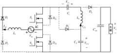
为实现上述目的,本发明所提供的技术方案为:一种单相高增益无桥功率因数校正变换器,包括有交流输入电源,第一电感,第一二极管,第二二极管,第一开关管及其寄生二极管,第二开关管及其寄生二极管,第三二极管,第二电感,第一电容,第二电容,第四二极管,输出电容;其中,所述交流输入电源的一端接第一电感的一端,其另一端分别与第一开关管的源极和第二开关管的漏极连接;所述第一电感的另一端分别接第一二极管的阳极和第二二极管的阴极;所述第一二极管的阴极分别与第一开关管的漏极、第一电容的一端和第三二极管的阳极连接;所述第一电容的另一端分别与第四二极管的阳极和第二电感的一端连接;所述第二电感的另一端分别与第三二极管的阴极和第二电容的一端连接;所述第四二极管的阴极分别与输出电容的一端和负载一端连接,负载的另一端分别与第二二极管的阳极、第二开关管的源极、第二电容的另一端、输出电容的另一端连接。In order to achieve the above object, the technical solution provided by the present invention is: a single-phase high-gain bridgeless power factor correction converter, including an AC input power supply, a first inductor, a first diode, a second diode, The first switch tube and its parasitic diode, the second switch tube and its parasitic diode, the third diode, the second inductor, the first capacitor, the second capacitor, the fourth diode, and the output capacitor; wherein, the AC One end of the input power supply is connected to one end of the first inductor, and the other end is respectively connected to the source of the first switching tube and the drain of the second switching tube; the other end of the first inductor is respectively connected to the anode of the first diode and the cathode of the second diode; the cathode of the first diode is respectively connected to the drain of the first switching tube, one end of the first capacitor and the anode of the third diode; the other of the first capacitor One end is respectively connected to the anode of the fourth diode and one end of the second inductance; the other end of the second inductance is respectively connected to the cathode of the third diode and one end of the second capacitor; the fourth diode The cathode of the cathode is respectively connected to one end of the output capacitor and one end of the load, and the other end of the load is respectively connected to the anode of the second diode, the source of the second switching tube, the other end of the second capacitor, and the other end of the output capacitor.
所述第一开关管和第二开关管的驱动信号一致。The driving signals of the first switching tube and the second switching tube are consistent.
所述第一开关管和第二开关管为具有逆导特性的功率开关管。The first switch tube and the second switch tube are power switch tubes with reverse conduction characteristics.
所述第一开关管和第二开关管为带反并联二极管的功率开关管。The first switch tube and the second switch tube are power switch tubes with anti-parallel diodes.
本发明与现有技术相比,具有如下优点与有益效果:Compared with the prior art, the present invention has the following advantages and beneficial effects:
1、利用开关管代替原有的整流桥中的两个二极管,在每半个工频周波中,只有一个二极管一直处于通态,提高了变换器的工作效率;1. Use the switch tube to replace the two diodes in the original rectifier bridge. In every half power frequency cycle, only one diode is always in the on state, which improves the working efficiency of the converter;
2、在每个工频半周波中,有一个开关管实现零电压开通和关断,另外一个开关管在关断时承受的电压小于输出电压,这也提高了变换器的工作效率;2. In each power frequency half-cycle, one switch tube realizes zero-voltage turn-on and turn-off, and the other switch tube bears a voltage lower than the output voltage when it is turned off, which also improves the working efficiency of the converter;
3、相比于传统单相BOOST功率因数校正变换器,稳态增益高,变换器需要较小的占空比即可输出同样的电压,在同样的输入电压下,本发明的输出电压范围更大。3. Compared with the traditional single-phase BOOST power factor correction converter, the steady-state gain is high, and the converter needs a smaller duty cycle to output the same voltage. Under the same input voltage, the output voltage range of the present invention is wider big.
附图说明Description of drawings
图1为本发明的电路原理图。Fig. 1 is the circuit schematic diagram of the present invention.
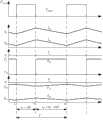
图2为交流输入电压正半周一个开关周期主要元件的电压电流波形图。Figure 2 is the voltage and current waveform diagram of the main components of a switching cycle in the positive half cycle of the AC input voltage.
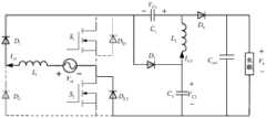
图3a为交流输入电压正半周一个开关周期内电路模态图之一。Fig. 3a is one of the circuit modal diagrams in a switching cycle in the positive half cycle of the AC input voltage.
图3b为交流输入电压正半周一个开关周期内电路模态图之二。Fig. 3b is the second modal diagram of the circuit in a switching cycle in the positive half cycle of the AC input voltage.
图4为交流输入电压负半周一个开关周期主要元件的电压电流波形图。Fig. 4 is a voltage and current waveform diagram of main components of a switching cycle in the negative half cycle of the AC input voltage.
图5a为交流输入电压负半周一个开关周期内电路模态图之一。Fig. 5a is one of the circuit modal diagrams in a switching cycle in the negative half cycle of the AC input voltage.
图5b为交流输入电压负半周一个开关周期内电路模态图之二。Fig. 5b is the second modal diagram of the circuit in a switching cycle in the negative half cycle of the AC input voltage.
图6为本发明的单相高增益无桥功率因数校正变换器与传统单相BOOST功率因数校正变换器的稳态增益对比图。FIG. 6 is a comparison chart of the steady-state gain between the single-phase high-gain bridgeless power factor correction converter of the present invention and the traditional single-phase BOOST power factor correction converter.
图7为第一电感的电流IL1仿真波形。FIG. 7 is a simulation waveform of the current IL1 of the first inductor.
图8为输出电压Vo和第一开关管的漏源极电压VS1仿真波形对比图。FIG. 8 is a comparison diagram of the simulated waveforms of the output voltage Vo and the drain-source voltage VS1 of the first switch tube.
图9为第一电感的电流IL1和输入电压Vin仿真波形图。FIG. 9 is a simulation waveform diagram of the current IL1 of the first inductor and the input voltage Vin .
具体实施方式Detailed ways
下面结合具体实施例对本发明作进一步说明。The present invention will be further described below in conjunction with specific examples.
如图1所示,本实施例所述的单相高增益无桥功率因数校正变换器,包括有交流输入电源AC,第一电感L1,第一二极管D1,第二二极管D2,第一开关管S1及其寄生二极管DS1,第二开关管S2及其寄生二极管DS2,第三二极管D3,第二电感L2,第一电容C1,第二电容C2,第四二极管D4,输出电容Cout;其中,所述交流输入电源AC的一端接第一电感L1的一端,其另一端分别与第一开关管S1的源极和第二开关管S2的漏极连接;所述第一电感L1的另一端分别接第一二极管D1的阳极和第二二极管D2的阴极;所述第一二极管D1的阴极分别与第一开关管S1的漏极、第一电容C1的一端和第三二极管D3的阳极连接;所述第一电容C1的另一端分别与第四二极管D4的阳极和第二电感L2的一端连接;所述第二电感L2的另一端分别与第三二极管D3的阴极和第二电容C2的一端连接;所述第四二极管D4的阴极分别与输出电容Cout的一端和负载一端连接,负载的另一端分别与第二二极管D2的阳极、第二开关管S2的源极、第二电容C2的另一端、输出电容Cout的另一端连接。所述第一开关管S1和第二开关管S2的驱动信号一致;该第一开关管S1和第二开关管S2可以是具有逆导特性的功率开关管,或带有反并联二极管的功率开关管。As shown in Figure 1, the single-phase high-gain bridgeless power factor correction converter described in this embodiment includes an AC input power supply AC, a first inductor L1 , a first diode D1 , and a second diode D2 , the first switching tube S1 and its parasitic diode DS1 , the second switching tube S2 and its parasitic diode DS2 , the third diode D3 , the second inductor L2 , the first capacitor C1 , the second Two capacitors C2 , fourth diode D4 , and output capacitor Cout ; wherein, one end of the AC input power source AC is connected to one end of the first inductor L1 , and the other end is connected to the source of the first switching tube S1 respectively. The pole is connected to the drain of the second switching tubeS2 ; the other end of the first inductorL1 is respectively connected to the anode of the first diodeD1 and the cathode of the second diodeD2 ; the first two The cathode of the pole tubeD1 is respectively connected to the drain of the first switching tubeS1 , one end of the first capacitorC1 and the anode of the third diodeD3 ; the other end of the first capacitorC1 is respectively connected to the first The anode of the four diodesD4 is connected to one end of the second inductanceL2 ; the other end of the second inductanceL2 is respectively connected to the cathode of the third diodeD3 and one end of the second capacitorC2 ; The cathode of the fourth diodeD4 is respectively connected to one end of the output capacitor Cout and one end of the load, and the other end of the load is respectively connected to the anode of the second diodeD2 , the source of the second switching tubeS2 , the first The other end of the second capacitor C2 is connected to the other end of the output capacitor Cout . The driving signals of the first switching tubeS1 and the second switching tubeS2 are consistent; the first switching tubeS1 and the second switching tubeS2 may be power switching tubes with reverse conduction characteristics, or have anti-parallel Diode power switch tube.
在本实施例中,本发明所述的单相高增益无桥功率因数校正变换器的具体情况如下:In this embodiment, the specific conditions of the single-phase high-gain bridgeless power factor correction converter described in the present invention are as follows:
1)、交流输入电源的正半周,即交流输入电压Vin左正右负1) The positive half cycle of the AC input power supply, that is, the AC input voltage Vin is positive on the left and negative on the right
在正半周内,第一二极管D1承受正向电压,一直处于导通状态,第二二极管D2承受反向电压,一直处于关断状态。在正半周中的一个开关周期中第一电感L1的电流IL1和第二电感L2的电流IL2、输出电压Vo、第一开关管S1的漏源极电压VS1、第一电容C1的电压VC1和第二电容C2的电压VC2波形图如图2所示。In the positive half cycle, the first diodeD1 bears the forward voltage and is always in the conduction state, and the second diodeD2 bears the reverse voltage and is always in the off state. In a switching cycle in the positive half cycle, the current IL1 of the first inductor L1 and the current IL2 of the second inductor L2 , the output voltage Vo , the drain-source voltage VS1 of the first switching tube S1 , the first The waveforms of the voltage VC1 of the capacitorC1 and the voltage VC2 of the second capacitorC2 are shown in FIG. 2 .
a、在阶段t0~t1,此阶段的模态图如图3a所示,在t0时刻,驱动信号从低电平变为高电平,第一开关管S1和第二开关管S2导通,第一开关管S1的寄生二极管DS1和第二开关管S2的寄生二极管DS2承受反向电压,处于关断状态。交流输入电压Vin通过第一开关管S1和第一二极管D1给第一电感L1充电。第二电容C2通过第一开关管S1和第二开关管S2给第二电感L2和第一电容C1充电。第四二极管D4承受反向电压,处于关断状态。输出电容Cout给负载供电,维持输出电压Vo恒定。a. In the stage t0 ~ t1 , the modal diagram of this stage is shown in Figure 3a. At the time t0 , the driving signal From low level to high level, the first switching tubeS1 and the second switching tubeS2 are turned on, and the parasitic diode DS1 of the first switching tubeS1 and the parasitic diode DS2 of the second switching tubeS2 bear Reverse voltage, in shutdown state. The AC input voltage Vin charges the first inductor L1 through the first switch tube S1 and the first diode D1 . The second capacitorC2 charges the second inductorL2 and the first capacitorC1 throughthe first switch S1 and the second switchS2 . The fourth diodeD4 bears the reverse voltage and is in an off state. The output capacitor Cout supplies power to the load and maintains the output voltage Vo constant.
b、在阶段t1~t2,此阶段的模态图如图3b所示,在t1时刻,驱动信号
2)、交流输入电源的负半周,即交流输入电压Vin左负右正2) The negative half cycle of the AC input power supply, that is, the AC input voltage Vin is negative on the left and positive on the right
在负半周内,第一二极管D1承受反向电压,一直处于关断状态,第二二极管D2承受正向电压,一直处于导通状态。此阶段的一个开关周期中第一电感L1的电流IL1和第二电感L2的电流IL2、输出电压Vo、第一开关管S1的漏源极电压VS1、第一电容C1的电压VC1和第二电容C2的电压VC2波形图如图4所示。In the negative half cycle, the first diode D1 is always in the off state under the reverse voltage, and the second diode D2 is under the forward voltage and is always in the on state. In one switching cycle of this stage, the current IL1 of the first inductor L1 and the current IL2 of the second inductor L2 , the output voltage Vo , the drain-source voltage VS1 of the first switching tube S1 , the first capacitor C The waveforms of the voltage VC1 of1 andthe voltage V C2of the second capacitor C2 are shown in FIG. 4 .
a、在阶段t0~t1,此阶段的模态图如图5a所示,在t0时刻,驱动信号
b、在阶段t1~t2,此阶段的模态图如图5b所示,在t1时刻,驱动信号
3)、稳态增益3) Steady-state gain
以交流输入电压的正半周为例分析一种高增益无桥变换器的稳态增益。第一电感L1的电压

第二电感L2的电压
而传统单相BOOST功率因数校正电路的稳态增益为1/(1-D)。本发明和传统单相BOOST功率因数校正电路VO/Vin随占空比D变化的波形图如图6所示,从图6可知,在相同的占空比和输入电压的条件下,本发明输出电压比传统单相BOOST功率因数校正电路输出电压还要高。However, the steady-state gain of the traditional single-phase BOOST power factor correction circuit is 1/(1-D). The present invention and the traditional single-phase BOOST power factor correction circuit VO /Vin change with the waveform diagram of the duty cycle D as shown in Figure 6, from Figure 6 we can see that under the same duty cycle and input voltage conditions, the present invention The output voltage of the invention is higher than the output voltage of the traditional single-phase BOOST power factor correction circuit.
下面对本发明实施进行仿真验证,设计参数如下:Carry out simulation verification to the implementation of the present invention below, design parameter is as follows:
输入电压:220V/50HzInput voltage: 220V/50Hz
功率因数:PF=0.99Power factor: PF=0.99
总谐波含量:THD≤5%Total harmonic content: THD≤5%
输出电压:500V/1.2AOutput voltage: 500V/1.2A
图7为输入电流,即第一电感L1的电流IL1的仿真波形,其谐波含量THD值为2.89%;输出电压Vo和第一开关管S1的漏源极电压VS1仿真波形对比如图8所示,可见第一开关管S1的漏源极电压VS1小于输出电压Vo;第一电感L1的电流IL1和输入电压Vin仿真波形图如图9所示,输入电流与输入电压的功率因数PF为0.9993,接近于1。Figure 7 is the simulation waveform of the input current, that is, the current IL1 of the first inductorL1 , whose harmonic content THD value is 2.89%; the simulation waveform of the output voltage Vo and the drain-source voltage VS1 of the first switching tubeS1 By comparison, as shown in Figure 8, it can be seen that the drain-source voltage VS1 of the first switch tubeS1 is smaller than the output voltage Vo ; the simulation waveform diagram of the current IL1 of the first inductorL1 and the input voltage Vin is shown in Figure 9, and the input The power factor PF of current and input voltage is 0.9993, which is close to 1.
以上所述之实施例子只为本发明之较佳实施例,并非以此限制本发明的实施范围,故凡依本发明之形状、原理所作的变化,均应涵盖在本发明的保护范围内。The implementation examples described above are only preferred embodiments of the present invention, and are not intended to limit the scope of the present invention. Therefore, all changes made according to the shape and principles of the present invention should be covered within the protection scope of the present invention.
Claims (4)
Priority Applications (1)
| Application Number | Priority Date | Filing Date | Title |
|---|---|---|---|
| CN201310526728.3ACN103546026B (en) | 2013-10-30 | 2013-10-30 | A kind of single-phase high-gain no-bridge power factor correction converter |
Applications Claiming Priority (1)
| Application Number | Priority Date | Filing Date | Title |
|---|---|---|---|
| CN201310526728.3ACN103546026B (en) | 2013-10-30 | 2013-10-30 | A kind of single-phase high-gain no-bridge power factor correction converter |
Publications (2)
| Publication Number | Publication Date |
|---|---|
| CN103546026Atrue CN103546026A (en) | 2014-01-29 |
| CN103546026B CN103546026B (en) | 2015-12-02 |
Family
ID=49969181
Family Applications (1)
| Application Number | Title | Priority Date | Filing Date |
|---|---|---|---|
| CN201310526728.3AActiveCN103546026B (en) | 2013-10-30 | 2013-10-30 | A kind of single-phase high-gain no-bridge power factor correction converter |
Country Status (1)
| Country | Link |
|---|---|
| CN (1) | CN103546026B (en) |
Cited By (3)
| Publication number | Priority date | Publication date | Assignee | Title |
|---|---|---|---|---|
| CN107332437A (en)* | 2017-08-21 | 2017-11-07 | 国网上海市电力公司 | A kind of single inductance is without bridge APFC circuits |
| CN110429837A (en)* | 2019-08-02 | 2019-11-08 | 矽力杰半导体技术(杭州)有限公司 | Wide scope input and output AC-DC converter |
| CN112953263A (en)* | 2021-03-18 | 2021-06-11 | 上海大学 | Negative output high-gain bridgeless switched capacitor SEPIC PFC converter |
Citations (3)
| Publication number | Priority date | Publication date | Assignee | Title |
|---|---|---|---|---|
| CN101728964A (en)* | 2010-01-12 | 2010-06-09 | 浙江大学 | Bridgeless power factor correction converter with single inductance and three levels |
| US20110149622A1 (en)* | 2009-12-22 | 2011-06-23 | Logah Technology Corp. | Interleaved Bridgeless Power Factor Corrector and Controlling Method thereof |
| CN203590015U (en)* | 2013-10-30 | 2014-05-07 | 华南理工大学 | Single-phase high-gain no-bridge power factor correction converter |
- 2013
- 2013-10-30CNCN201310526728.3Apatent/CN103546026B/enactiveActive
Patent Citations (3)
| Publication number | Priority date | Publication date | Assignee | Title |
|---|---|---|---|---|
| US20110149622A1 (en)* | 2009-12-22 | 2011-06-23 | Logah Technology Corp. | Interleaved Bridgeless Power Factor Corrector and Controlling Method thereof |
| CN101728964A (en)* | 2010-01-12 | 2010-06-09 | 浙江大学 | Bridgeless power factor correction converter with single inductance and three levels |
| CN203590015U (en)* | 2013-10-30 | 2014-05-07 | 华南理工大学 | Single-phase high-gain no-bridge power factor correction converter |
Non-Patent Citations (1)
| Title |
|---|
| 陆治国等: "一种改进的单相无桥功率因数校正器", 《电力电子技术》* |
Cited By (4)
| Publication number | Priority date | Publication date | Assignee | Title |
|---|---|---|---|---|
| CN107332437A (en)* | 2017-08-21 | 2017-11-07 | 国网上海市电力公司 | A kind of single inductance is without bridge APFC circuits |
| CN107332437B (en)* | 2017-08-21 | 2023-09-15 | 国网上海市电力公司 | Single-inductor bridgeless APFC circuit |
| CN110429837A (en)* | 2019-08-02 | 2019-11-08 | 矽力杰半导体技术(杭州)有限公司 | Wide scope input and output AC-DC converter |
| CN112953263A (en)* | 2021-03-18 | 2021-06-11 | 上海大学 | Negative output high-gain bridgeless switched capacitor SEPIC PFC converter |
Also Published As
| Publication number | Publication date |
|---|---|
| CN103546026B (en) | 2015-12-02 |
Similar Documents
| Publication | Publication Date | Title |
|---|---|---|
| CN108900100B (en) | A kind of single-phase high efficiency high frequency isolated form rectifier | |
| CN103066873B (en) | Novel voltage reduction type bridgeless Cuk power factor correction (PFC) circuit | |
| CN107994789A (en) | A kind of isolated form integrated form AC-DC converter based on non-bridge PFC and LLC resonance | |
| CN108183603B (en) | A kind of single-stage is without bridge Sofe Switch resonance isolated form circuit of power factor correction | |
| CN101515762B (en) | Passive clamping single-phase single-grade bridge type power factor correcting convertor and control method thereof | |
| CN104202862B (en) | Single-stage type LED drive power supply without electrolytic capacitor | |
| CN101917131A (en) | Cascaded Buck-boost high power factor AC-DC converter and its conversion method | |
| CN106533152A (en) | Device and method for improving PF of Boost three-level converter | |
| CN112332652B (en) | Bridgeless power factor correction circuit based on resonant switch capacitor converter | |
| CN103683952B (en) | A kind of integration in parallel connection formula Buck-Flyback power factor correction pfc converter topology | |
| CN207868995U (en) | A kind of high-power factor half bridge series resonance DC/DC converters | |
| CN103762839B (en) | A kind of magnetic coupling type single-phase high-gain Bridgeless power factor circuit correcting circuit | |
| CN103546026B (en) | A kind of single-phase high-gain no-bridge power factor correction converter | |
| CN204442168U (en) | A kind of based on without bridge CUK isolated form Three Phase Power Factor Correction Converter | |
| CN103546041A (en) | Main circuit topology of three-level flyback converter | |
| CN105429452A (en) | A Common Mode Rejection Dual Boost Bridgeless PFC Converter | |
| CN205212694U (en) | Two boost of common mode rejection do not have bridge PFC converter | |
| CN203339946U (en) | LCD absorption circuit | |
| CN102710117B (en) | High-efficiency passive power factor correction circuit | |
| CN206743105U (en) | Positive activation type five-electrical level inverter | |
| CN206180891U (en) | High -efficient light stores up self -supporting formula energy storage converter of uniting | |
| CN205336138U (en) | Two boost voltage -multiplying PFC converters of high efficiency | |
| CN101257250B (en) | Transformer primary voltage nip bit three phase single-stage bridge type power factor correcting converter | |
| CN104967304A (en) | An isolated three-phase power factor correction converter based on bridgeless CUK | |
| CN115276431A (en) | A new type of power converter in electric vehicle power system |
Legal Events
| Date | Code | Title | Description |
|---|---|---|---|
| C06 | Publication | ||
| PB01 | Publication | ||
| SE01 | Entry into force of request for substantive examination | ||
| SE01 | Entry into force of request for substantive examination | ||
| C14 | Grant of patent or utility model | ||
| GR01 | Patent grant |