CN103514834A - pixels for a display - Google Patents
pixels for a displayDownload PDFInfo
- Publication number
- CN103514834A CN103514834ACN201310116389.1ACN201310116389ACN103514834ACN 103514834 ACN103514834 ACN 103514834ACN 201310116389 ACN201310116389 ACN 201310116389ACN 103514834 ACN103514834 ACN 103514834A
- Authority
- CN
- China
- Prior art keywords
- transistor
- pixel
- terminal
- switch
- current
- Prior art date
- Legal status (The legal status is an assumption and is not a legal conclusion. Google has not performed a legal analysis and makes no representation as to the accuracy of the status listed.)
- Granted
Links
Images


Classifications
- G—PHYSICS
- G09—EDUCATION; CRYPTOGRAPHY; DISPLAY; ADVERTISING; SEALS
- G09G—ARRANGEMENTS OR CIRCUITS FOR CONTROL OF INDICATING DEVICES USING STATIC MEANS TO PRESENT VARIABLE INFORMATION
- G09G3/00—Control arrangements or circuits, of interest only in connection with visual indicators other than cathode-ray tubes
- G09G3/20—Control arrangements or circuits, of interest only in connection with visual indicators other than cathode-ray tubes for presentation of an assembly of a number of characters, e.g. a page, by composing the assembly by combination of individual elements arranged in a matrix no fixed position being assigned to or needed to be assigned to the individual characters or partial characters
- G09G3/22—Control arrangements or circuits, of interest only in connection with visual indicators other than cathode-ray tubes for presentation of an assembly of a number of characters, e.g. a page, by composing the assembly by combination of individual elements arranged in a matrix no fixed position being assigned to or needed to be assigned to the individual characters or partial characters using controlled light sources
- G09G3/30—Control arrangements or circuits, of interest only in connection with visual indicators other than cathode-ray tubes for presentation of an assembly of a number of characters, e.g. a page, by composing the assembly by combination of individual elements arranged in a matrix no fixed position being assigned to or needed to be assigned to the individual characters or partial characters using controlled light sources using electroluminescent panels
- G09G3/32—Control arrangements or circuits, of interest only in connection with visual indicators other than cathode-ray tubes for presentation of an assembly of a number of characters, e.g. a page, by composing the assembly by combination of individual elements arranged in a matrix no fixed position being assigned to or needed to be assigned to the individual characters or partial characters using controlled light sources using electroluminescent panels semiconductive, e.g. using light-emitting diodes [LED]
- G09G3/3208—Control arrangements or circuits, of interest only in connection with visual indicators other than cathode-ray tubes for presentation of an assembly of a number of characters, e.g. a page, by composing the assembly by combination of individual elements arranged in a matrix no fixed position being assigned to or needed to be assigned to the individual characters or partial characters using controlled light sources using electroluminescent panels semiconductive, e.g. using light-emitting diodes [LED] organic, e.g. using organic light-emitting diodes [OLED]
- G09G3/3225—Control arrangements or circuits, of interest only in connection with visual indicators other than cathode-ray tubes for presentation of an assembly of a number of characters, e.g. a page, by composing the assembly by combination of individual elements arranged in a matrix no fixed position being assigned to or needed to be assigned to the individual characters or partial characters using controlled light sources using electroluminescent panels semiconductive, e.g. using light-emitting diodes [LED] organic, e.g. using organic light-emitting diodes [OLED] using an active matrix
- G09G3/3233—Control arrangements or circuits, of interest only in connection with visual indicators other than cathode-ray tubes for presentation of an assembly of a number of characters, e.g. a page, by composing the assembly by combination of individual elements arranged in a matrix no fixed position being assigned to or needed to be assigned to the individual characters or partial characters using controlled light sources using electroluminescent panels semiconductive, e.g. using light-emitting diodes [LED] organic, e.g. using organic light-emitting diodes [OLED] using an active matrix with pixel circuitry controlling the current through the light-emitting element
- G—PHYSICS
- G09—EDUCATION; CRYPTOGRAPHY; DISPLAY; ADVERTISING; SEALS
- G09G—ARRANGEMENTS OR CIRCUITS FOR CONTROL OF INDICATING DEVICES USING STATIC MEANS TO PRESENT VARIABLE INFORMATION
- G09G3/00—Control arrangements or circuits, of interest only in connection with visual indicators other than cathode-ray tubes
- G09G3/20—Control arrangements or circuits, of interest only in connection with visual indicators other than cathode-ray tubes for presentation of an assembly of a number of characters, e.g. a page, by composing the assembly by combination of individual elements arranged in a matrix no fixed position being assigned to or needed to be assigned to the individual characters or partial characters
- G09G3/34—Control arrangements or circuits, of interest only in connection with visual indicators other than cathode-ray tubes for presentation of an assembly of a number of characters, e.g. a page, by composing the assembly by combination of individual elements arranged in a matrix no fixed position being assigned to or needed to be assigned to the individual characters or partial characters by control of light from an independent source
- G09G3/3406—Control of illumination source
- G—PHYSICS
- G09—EDUCATION; CRYPTOGRAPHY; DISPLAY; ADVERTISING; SEALS
- G09G—ARRANGEMENTS OR CIRCUITS FOR CONTROL OF INDICATING DEVICES USING STATIC MEANS TO PRESENT VARIABLE INFORMATION
- G09G2300/00—Aspects of the constitution of display devices
- G09G2300/08—Active matrix structure, i.e. with use of active elements, inclusive of non-linear two terminal elements, in the pixels together with light emitting or modulating elements
- G09G2300/0809—Several active elements per pixel in active matrix panels
- G09G2300/0819—Several active elements per pixel in active matrix panels used for counteracting undesired variations, e.g. feedback or autozeroing
- G—PHYSICS
- G09—EDUCATION; CRYPTOGRAPHY; DISPLAY; ADVERTISING; SEALS
- G09G—ARRANGEMENTS OR CIRCUITS FOR CONTROL OF INDICATING DEVICES USING STATIC MEANS TO PRESENT VARIABLE INFORMATION
- G09G2300/00—Aspects of the constitution of display devices
- G09G2300/08—Active matrix structure, i.e. with use of active elements, inclusive of non-linear two terminal elements, in the pixels together with light emitting or modulating elements
- G09G2300/0809—Several active elements per pixel in active matrix panels
- G09G2300/0842—Several active elements per pixel in active matrix panels forming a memory circuit, e.g. a dynamic memory with one capacitor
- G—PHYSICS
- G09—EDUCATION; CRYPTOGRAPHY; DISPLAY; ADVERTISING; SEALS
- G09G—ARRANGEMENTS OR CIRCUITS FOR CONTROL OF INDICATING DEVICES USING STATIC MEANS TO PRESENT VARIABLE INFORMATION
- G09G2320/00—Control of display operating conditions
- G09G2320/02—Improving the quality of display appearance
- G09G2320/0233—Improving the luminance or brightness uniformity across the screen
- G—PHYSICS
- G09—EDUCATION; CRYPTOGRAPHY; DISPLAY; ADVERTISING; SEALS
- G09G—ARRANGEMENTS OR CIRCUITS FOR CONTROL OF INDICATING DEVICES USING STATIC MEANS TO PRESENT VARIABLE INFORMATION
- G09G2320/00—Control of display operating conditions
- G09G2320/02—Improving the quality of display appearance
- G09G2320/029—Improving the quality of display appearance by monitoring one or more pixels in the display panel, e.g. by monitoring a fixed reference pixel
- G09G2320/0295—Improving the quality of display appearance by monitoring one or more pixels in the display panel, e.g. by monitoring a fixed reference pixel by monitoring each display pixel
- G—PHYSICS
- G09—EDUCATION; CRYPTOGRAPHY; DISPLAY; ADVERTISING; SEALS
- G09G—ARRANGEMENTS OR CIRCUITS FOR CONTROL OF INDICATING DEVICES USING STATIC MEANS TO PRESENT VARIABLE INFORMATION
- G09G2320/00—Control of display operating conditions
- G09G2320/04—Maintaining the quality of display appearance
- G09G2320/043—Preventing or counteracting the effects of ageing
- G09G2320/045—Compensation of drifts in the characteristics of light emitting or modulating elements
- G—PHYSICS
- G09—EDUCATION; CRYPTOGRAPHY; DISPLAY; ADVERTISING; SEALS
- G09G—ARRANGEMENTS OR CIRCUITS FOR CONTROL OF INDICATING DEVICES USING STATIC MEANS TO PRESENT VARIABLE INFORMATION
- G09G2330/00—Aspects of power supply; Aspects of display protection and defect management
- G09G2330/02—Details of power systems and of start or stop of display operation
- G09G2330/028—Generation of voltages supplied to electrode drivers in a matrix display other than LCD
Landscapes
- Engineering & Computer Science (AREA)
- Physics & Mathematics (AREA)
- Computer Hardware Design (AREA)
- General Physics & Mathematics (AREA)
- Theoretical Computer Science (AREA)
- Control Of Indicators Other Than Cathode Ray Tubes (AREA)
- Control Of El Displays (AREA)
- Electroluminescent Light Sources (AREA)
Abstract
Description
Translated fromChinese技术领域technical field
本公开涉及用于显示器的像素。This disclosure relates to pixels for displays.
背景技术Background technique
在包括柔性显示器的显示器中使用的有源矩阵有机发光二极管(AM-OLED)丰富了电视观众的数字内容的体验。通常,与诸如薄膜晶体管液晶(TFT-LCD)显示器的其他显示器相比,AM-OLED显示器更薄、更亮、具有更宽视角以及消耗更低功率。然而,AM-OLED更加昂贵,要求良好的像素均匀性,并且更难制造。Active-matrix organic light-emitting diodes (AM-OLEDs) used in displays, including flexible displays, enrich the television viewer's experience with digital content. In general, AM-OLED displays are thinner, brighter, have wider viewing angles, and consume less power than other displays such as Thin Film Transistor Liquid Crystal (TFT-LCD) displays. However, AM-OLED is more expensive, requires good pixel uniformity, and is more difficult to manufacture.
包括多晶硅TFT和金属氧化物TFT的薄膜晶体管(TFT)是用于AM-OLED TFT显示器的像素电路的良好候选者。然而,用于显示器的TFT基板通常由玻璃或塑料制成,其通常不耐高温(诸如用于结晶处理的600℃)。Thin film transistors (TFTs) including polysilicon TFTs and metal oxide TFTs are good candidates for pixel circuits in AM-OLED TFT displays. However, TFT substrates for displays are generally made of glass or plastic, which are generally not resistant to high temperatures (such as 600°C for crystallization processing).
显示器包括布置为行和列的多个像素。现有像素电路包括多个TFT,从而导致较大的像素尺寸、较低的分辨率以及较高的功耗。The display includes a plurality of pixels arranged in rows and columns. Existing pixel circuits include multiple TFTs, resulting in larger pixel size, lower resolution, and higher power consumption.
发明内容Contents of the invention
根据本发明的一个方面,提供了一种增加显示器中的第一像素和第二像素之间的亮度均匀性的方法,包括:确定第一像素的电流值;确定第二像素的电流值;以及调节第一像素的电流值或第二像素的电流值中的至少一个,直到第一像素的电流值和第二像素的电流值之间的电流差值在预定范围内,其中,第一像素的电流值对应于第一像素的发光二级管(LED)的亮度级并且由第一像素的晶体管提供;第二像素的电流值对应于第二像素的LED的亮度级并且由第二像素的晶体管提供;调节第一像素的电流值包括调节第一像素的晶体管的阈值电压值;以及调节第二像素的电流值包括调节第二像素的晶体管的阈值电压值。According to one aspect of the present invention, there is provided a method of increasing brightness uniformity between a first pixel and a second pixel in a display, comprising: determining a current value of the first pixel; determining a current value of the second pixel; and adjusting at least one of the current value of the first pixel or the current value of the second pixel until the current difference between the current value of the first pixel and the current value of the second pixel is within a predetermined range, wherein the current value of the first pixel The current value corresponds to the brightness level of the light-emitting diode (LED) of the first pixel and is provided by the transistor of the first pixel; the current value of the second pixel corresponds to the brightness level of the LED of the second pixel and is provided by the transistor of the second pixel. It is provided that adjusting the current value of the first pixel includes adjusting a threshold voltage value of a transistor of the first pixel; and adjusting the current value of the second pixel includes adjusting a threshold voltage value of a transistor of the second pixel.
优选地,该方法进一步包括以下条件中的至少一个:第一像素的晶体管具有影响第一像素的晶体管的阈值电压值的浮栅存储电荷;或者第二像素的晶体管具有影响第二像素的晶体管的阈值电压值的浮栅存储电荷。Preferably, the method further includes at least one of the following conditions: the transistor of the first pixel has a floating gate stored charge that affects the threshold voltage value of the transistor of the first pixel; The floating gate stores charge at the threshold voltage value.
优选地,该方法进一步包括以下条件中的至少一个:调节第一像素的晶体管的阈值电压值包括调节第一像素的晶体管的浮栅中的电荷;或者调节第二像素的晶体管的阈值电压值包括调节第二像素的晶体管的浮栅中的电荷。Preferably, the method further includes at least one of the following conditions: adjusting the threshold voltage value of the transistor of the first pixel includes adjusting the charge in the floating gate of the transistor of the first pixel; or adjusting the threshold voltage value of the transistor of the second pixel includes The charge in the floating gate of the transistor of the second pixel is adjusted.
优选地,该方法进一步包括以下条件中的至少一个:调节第一像素的电流值进一步包括:在第一时间段内将第一电压施加至第一晶体管的第一端子,同时将第二电压值施加至第一晶体管的第二端子并且将第三电压值施加至第一晶体管的第三端子;或者调节第二像素的电流值进一步包括:在第二时间段内将第四电压施加至第二晶体管的第一端子,同时将第五电压值施加至第二晶体管的第二端子并且将第六电压值施加至第二晶体管的第三端子。Preferably, the method further includes at least one of the following conditions: adjusting the current value of the first pixel further includes: applying the first voltage to the first terminal of the first transistor within the first time period, and simultaneously applying the second voltage value applied to the second terminal of the first transistor and applying the third voltage value to the third terminal of the first transistor; or adjusting the current value of the second pixel further includes: applying a fourth voltage to the second the first terminal of the transistor while applying the fifth voltage value to the second terminal of the second transistor and the sixth voltage value to the third terminal of the second transistor.
优选地,该方法进一步包括以下条件中的至少一个:通过与第一晶体管的第一端子耦合的第一开关,将第一电压施加至第一晶体管的第一端子;以及通过与第一晶体管的第二端子耦合的第二开关,将第二电压施加至第一晶体管的第二端子;或者通过与第二晶体管的第一端子耦合的第三开关,将第三电压施加至第二晶体管的第一端子;以及通过与第二晶体管的第二端子耦合的第四开关,将第四电压施加至第二晶体管的第二端子。Preferably, the method further comprises at least one of: applying a first voltage to the first terminal of the first transistor via a first switch coupled to the first terminal of the first transistor; A second switch coupled to the second terminal applies a second voltage to the second terminal of the first transistor; or a third switch coupled to the first terminal of the second transistor applies a third voltage to the second terminal of the second transistor. a terminal; and applying a fourth voltage to the second terminal of the second transistor through a fourth switch coupled to the second terminal of the second transistor.
优选地,该方法进一步包括以下条件中的至少一个:调节第一像素的电流值包括补偿第一像素的LED的劣化;或者调节第二像素的电流值包括补偿第二像素的LED的劣化。Preferably, the method further includes at least one of the following conditions: adjusting the current value of the first pixel includes compensating for degradation of an LED of the first pixel; or adjusting the current value of the second pixel includes compensating for degradation of an LED of the second pixel.
优选地,该方法进一步包括以下条件中的至少一个:基于通过第一开关施加到第一像素的第一晶体管的第一端子的第一电压,截止第一像素的第一晶体管;基于流过第二开关和第一像素的LED的电流,确定第二开关的端子处的第二电压;以及第二开关与所述第一像素的LED和第一像素的第一晶体管耦合;或者基于通过第三开关施加至第一像素的第一晶体管的第一端子的第一电压,截止第二像素的第一晶体管;基于流过第四开关和第二像素的LED的电流,确定第四开关的端子处的第二电压;以及第四开关与第二像素的LED和第二像素的第一晶体管耦合。Preferably, the method further includes at least one of the following conditions: based on a first voltage applied to the first terminal of the first transistor of the first pixel through the first switch, turning off the first transistor of the first pixel; The current of the second switch and the LED of the first pixel determines a second voltage at the terminals of the second switch; and the second switch is coupled with the LED of the first pixel and the first transistor of the first pixel; or based on the current through the third the switch applies a first voltage to the first terminal of the first transistor of the first pixel, turning off the first transistor of the second pixel; based on the current flowing through the fourth switch and the LED of the second pixel, determining the position at the terminal of the fourth switch and a fourth switch coupled to the LED of the second pixel and the first transistor of the second pixel.
根据本发明的另一方面,提供了一种显示器的像素电路,包括:第一晶体管,具有第一端子、第二端子和第三端子;第一开关;第二开关;以及发光二极管,其中,第一晶体管的阈值电压可调节;第一晶体管的第一端子与第一开关耦合;像素电路被配置成满足以下条件中的至少一个:LED的第一端与第二开关和第一晶体管的第三端子耦合;或者LED的第二端与第二开关和第一晶体管的第二端子耦合。According to another aspect of the present invention, there is provided a pixel circuit of a display, comprising: a first transistor having a first terminal, a second terminal and a third terminal; a first switch; a second switch; and a light emitting diode, wherein, The threshold voltage of the first transistor is adjustable; the first terminal of the first transistor is coupled to the first switch; the pixel circuit is configured to meet at least one of the following conditions: the first terminal of the LED is connected to the second switch and the first terminal of the first transistor three-terminal coupling; or the second terminal of the LED is coupled with the second switch and the second terminal of the first transistor.
优选地,像素电路被配置成满足第一组条件、第二组条件、第三组条件和第四组条件中的至少一个。第一组条件包括:第一晶体管是第一PMOS晶体管,第一开关包括第二PMOS晶体管,并且第二开关包括第三PMOS晶体管;第一PMOS晶体管的栅极与第二PMOS晶体管耦合;以及第一PMOS晶体管的漏极与LED的正端子和第三PMOS晶体管耦合。第二组条件包括:第一晶体管是第一PMOS晶体管,第一开关包括第二PMOS晶体管,并且第二开关包括第三PMOS晶体管;第一PMOS晶体管的栅极与第二PMOS晶体管耦合;以及第一PMOS晶体管的源极与LED的负端子和第三PMOS晶体管耦合。第三组条件包括:第一晶体管是第一NMOS晶体管,第一开关包括第二NMOS晶体管,并且第二开关包括第三NMOS晶体管;第一NMOS晶体管的栅极与第二NMOS晶体管耦合;以及第一NMOS晶体管的漏极与LED的负端子和第三NMOS晶体管耦合。第四组条件包括:第一晶体管是第一NMOS晶体管,第一开关包括第二NMOS晶体管,并且第二开关包括所述第三NMOS晶体管;第一NMOS晶体管的栅极与第二NMOS晶体管耦合;以及第一NMOS晶体管的源极与LED的正端子和第三NMOS晶体管耦合。Preferably, the pixel circuit is configured to satisfy at least one of the first set of conditions, the second set of conditions, the third set of conditions and the fourth set of conditions. The first set of conditions includes: the first transistor is a first PMOS transistor, the first switch includes a second PMOS transistor, and the second switch includes a third PMOS transistor; the gate of the first PMOS transistor is coupled to the second PMOS transistor; and A drain of a PMOS transistor is coupled to the positive terminal of the LED and a third PMOS transistor. The second set of conditions includes: the first transistor is a first PMOS transistor, the first switch includes a second PMOS transistor, and the second switch includes a third PMOS transistor; the gate of the first PMOS transistor is coupled to the second PMOS transistor; and A source of a PMOS transistor is coupled to the negative terminal of the LED and a third PMOS transistor. The third set of conditions includes: the first transistor is a first NMOS transistor, the first switch includes a second NMOS transistor, and the second switch includes a third NMOS transistor; the gate of the first NMOS transistor is coupled to the second NMOS transistor; and A drain of an NMOS transistor is coupled to the negative terminal of the LED and a third NMOS transistor. The fourth set of conditions includes: the first transistor is a first NMOS transistor, the first switch includes a second NMOS transistor, and the second switch includes the third NMOS transistor; the gate of the first NMOS transistor is coupled to the second NMOS transistor; And the source of the first NMOS transistor is coupled to the positive terminal of the LED and the third NMOS transistor.
优选地,第一晶体管选自由薄膜晶体管、低温多晶硅晶体管、金属氧化物晶体管、氢化非晶硅(a-Si:H)晶体管、微晶硅晶体管和有机晶体管所组成的组。Preferably, the first transistor is selected from the group consisting of thin film transistors, low temperature polysilicon transistors, metal oxide transistors, hydrogenated amorphous silicon (a-Si:H) transistors, microcrystalline silicon transistors and organic transistors.
优选地,第一晶体管包括:浮栅,被配置成存储影响第一晶体管的阈值电压的电压值的电荷。Preferably, the first transistor includes: a floating gate configured to store charges of a voltage value affecting a threshold voltage of the first transistor.
优选地,像素电路进一步包括:稳定电路,与第一晶体管的第一端子耦合并且被配置成稳定第一晶体管的第一端子处的电压。Preferably, the pixel circuit further comprises: a stabilization circuit coupled to the first terminal of the first transistor and configured to stabilize the voltage at the first terminal of the first transistor.
优选地,稳定电路包括电容器件;电容器件的第一端与第一晶体管的第一端子耦合;以及电容器件的第二端与第一器件的第二端子耦合或者被配置成接收电压。Preferably, the stabilization circuit includes a capacitive device; a first terminal of the capacitive device coupled to the first terminal of the first transistor; and a second terminal of the capacitive device coupled to the second terminal of the first device or configured to receive a voltage.
优选地,第一开关被配置成将信号传送到第一晶体管的第一端子;以及基于从第一开关传送的信号的电压,调节第一晶体管的阈值电压。Preferably, the first switch is configured to transmit a signal to the first terminal of the first transistor; and to adjust the threshold voltage of the first transistor based on the voltage of the signal transmitted from the first switch.
优选地,第二开关被配置为用于从第一晶体管生成并且流过第二开关的电流的电流路径;以及基于电流调节所述第一晶体管的阈值电压。Preferably, the second switch is configured as a current path for a current generated from the first transistor and flowing through the second switch; and a threshold voltage of the first transistor is adjusted based on the current.
优选地,第二开关被配置为用于流过第二开关和所述LED的电流的电流路径。Preferably, the second switch is configured as a current path for a current flowing through the second switch and said LED.
优选地,LED是有机LED或有源矩阵有机LED。Preferably, the LEDs are organic LEDs or active matrix organic LEDs.
根据本发明的又一方面,提供了一种显示器的像素电路,包括:第一晶体管;第一开关;第二开关;以及发光二极管,其中,第一晶体管被配置成提供用于LED的电流;LED的亮度级基于由第一晶体管提供的电流的电流值;第一开关被配置成将信号提供给第一晶体管的浮栅;由第一开关提供的信号用于调节第一晶体管的浮栅中的电荷;第二开关被配置为第一电流路径和/或第二电流路径;第一电流路径被配置用于由第一晶体管提供并且流过第二开关的电流使用;以及第二电流路径被配置用于由流过第二开关和LED的电流使用。According to still another aspect of the present invention, there is provided a pixel circuit of a display, comprising: a first transistor; a first switch; a second switch; and a light emitting diode, wherein the first transistor is configured to provide a current for the LED; The brightness level of the LED is based on the current value of the current provided by the first transistor; the first switch is configured to provide a signal to the floating gate of the first transistor; the signal provided by the first switch is used to adjust the current in the floating gate of the first transistor The second switch is configured as the first current path and/or the second current path; the first current path is configured for use by the current provided by the first transistor and flowing through the second switch; and the second current path is configured by configured for use by current flowing through the second switch and the LED.
优选地,像素电路被配置成满足第一组条件、第二组条件、第三组条件和第四组条件中的至少一个。第一组条件包括:第一晶体管是第一PMOS晶体管,第一开关包括第二PMOS晶体管,以及第二开关包括第三PMOS晶体管;第一PMOS晶体管的栅极与第二PMOS晶体管耦合;以及第一PMOS晶体管的漏极与LED的正端子和第三PMOS晶体管耦合。第二组条件包括:第一晶体管是第一PMOS晶体管,第一开关包括第二PMOS晶体管,以及第二开关包括第三PMOS晶体管;第一PMOS晶体管的栅极与第二PMOS晶体管耦合;以及第一PMOS晶体管的源极与LED的负端子和所述第三PMOS晶体管耦合。第三组条件包括:第一晶体管是第一NMOS晶体管,第一开关包括第二NMOS晶体管,以及第二开关包括第三NMOS晶体管;第一NMOS晶体管的栅极与第二NMOS晶体管耦合;以及第一NMOS晶体管的漏极与LED的负端子和第三NMOS晶体管耦合。第四组条件包括:第一晶体管是第一NMOS晶体管,第一开关包括第二NMOS晶体管,并且第二开关包括所述第三NMOS晶体管;第一NMOS晶体管的栅极与第二NMOS晶体管耦合;以及第一NMOS晶体管的源极与LED的正端子和第三NMOS晶体管耦合。Preferably, the pixel circuit is configured to satisfy at least one of the first set of conditions, the second set of conditions, the third set of conditions and the fourth set of conditions. The first set of conditions includes: the first transistor is a first PMOS transistor, the first switch includes a second PMOS transistor, and the second switch includes a third PMOS transistor; the gate of the first PMOS transistor is coupled to the second PMOS transistor; and A drain of a PMOS transistor is coupled to the positive terminal of the LED and a third PMOS transistor. The second set of conditions includes: the first transistor is a first PMOS transistor, the first switch includes a second PMOS transistor, and the second switch includes a third PMOS transistor; the gate of the first PMOS transistor is coupled to the second PMOS transistor; and A source of a PMOS transistor is coupled to the negative terminal of the LED and the third PMOS transistor. The third set of conditions includes: the first transistor is a first NMOS transistor, the first switch includes a second NMOS transistor, and the second switch includes a third NMOS transistor; the gate of the first NMOS transistor is coupled to the second NMOS transistor; and A drain of an NMOS transistor is coupled to the negative terminal of the LED and a third NMOS transistor. The fourth set of conditions includes: the first transistor is a first NMOS transistor, the first switch includes a second NMOS transistor, and the second switch includes the third NMOS transistor; the gate of the first NMOS transistor is coupled to the second NMOS transistor; And the source of the first NMOS transistor is coupled to the positive terminal of the LED and the third NMOS transistor.
优选地,该像素电路进一步包括:稳定电路,与第一晶体管的第一端子耦合并且被配置成稳定第一晶体管的第一端子处的电压。Preferably, the pixel circuit further comprises: a stabilization circuit coupled to the first terminal of the first transistor and configured to stabilize the voltage at the first terminal of the first transistor.
优选地,稳定电路包括电容器件;电容器件的第一端与第一晶体管的第一端子耦合;以及电容器件的第二端与第一器件的第二端子耦合或者被配置成接收电压。Preferably, the stabilization circuit includes a capacitive device; a first terminal of the capacitive device coupled to the first terminal of the first transistor; and a second terminal of the capacitive device coupled to the second terminal of the first device or configured to receive a voltage.
优选地,第一晶体管选自由薄膜晶体管、低温多晶硅晶体管、金属氧化物晶体管、氢化非晶硅(a-Si:H)晶体管、微晶硅晶体管和有机晶体管所组成的组。Preferably, the first transistor is selected from the group consisting of thin film transistors, low temperature polysilicon transistors, metal oxide transistors, hydrogenated amorphous silicon (a-Si:H) transistors, microcrystalline silicon transistors and organic transistors.
优选地,LED是有机LED或者有源矩阵有机LED。Preferably, the LEDs are organic LEDs or active matrix organic LEDs.
附图说明Description of drawings
本公开的一个或多个实施例的详情在附图和以下说明中阐明。其他特征和优点将从说明书、附图和权利要求变得明显。The details of one or more embodiments of the disclosure are set forth in the accompanying drawings and the description below. Other features and advantages will be apparent from the description, drawings, and claims.
图1是根据一些实施例的像素阵列电路的示意图。FIG. 1 is a schematic diagram of a pixel array circuit according to some embodiments.
图2是根据一些实施例的像素电路或像素的示意图。Figure 2 is a schematic diagram of a pixel circuit or pixel according to some embodiments.
图3至图5是根据不同实施例的不同像素的示意图。3 to 5 are schematic diagrams of different pixels according to different embodiments.
图6是示出根据一些实施例的基于两个像素的电流电压(I-V)关系的两个像素的亮度的曲线图。FIG. 6 is a graph illustrating the brightness of two pixels based on the current-voltage (I-V) relationship of the two pixels, according to some embodiments.
图7是根据一些实施例的增加两个像素的亮度均匀性的方法的流程图。7 is a flowchart of a method of increasing brightness uniformity of two pixels, according to some embodiments.
多个图中的类似参考符号指示类似元件。Similar reference symbols in several drawings indicate similar elements.
具体实施方式Detailed ways
以下使用特定语言公开图中示出的实施例或实例。然而,将理解,实施例和实例不用于限制。所公开的实施例中的任何更改和修改以及本文中公开的原理的任何进一步应用都认为是对本领域普通技术人员显而易见。The embodiments or examples shown in the drawings are disclosed below using specific language. However, it will be understood that the embodiments and examples are not intended to be limiting. Any alterations and modifications in the disclosed embodiments, as well as any further applications of the principles disclosed herein, are deemed to be apparent to those of ordinary skill in the art.
一些实施例具有以下特征和/或优点中的一个或结合。像素中的薄膜晶体管(TFT)的电流被用于控制相同像素中的相应LED的亮度。晶体管的阈值电压(VTH)可调节。从而,基于阈值电压VTH由晶体管生成的电流可调节。在一些实施例中,两个像素中的两个晶体管的阈值电压VTH的值被调节为相互更接近。有效地,两个像素中的两个晶体管的电流相互更接近。结果,两个像素的亮度相互更接近。换句话说,两个像素的亮度更加均匀,从而像素显示器的亮度更加均匀。与一些现有方法相比,在本公开的多种实施例中,在像素中使用较少数量的晶体管,从而得到用于像素的较小管芯面积和用于显示器的较高分辨率。例如,在一些实施例中,与另一种方法中使用四个晶体管和两个电容器相比,在像素中使用具有电容器的三个晶体管。不使用能量补偿方案,从而获得较低的功耗。Some embodiments have one or a combination of the following features and/or advantages. The current of a thin film transistor (TFT) in a pixel is used to control the brightness of a corresponding LED in the same pixel. The threshold voltage (VTH) of the transistor is adjustable. Thus, the current generated by the transistor is adjustable based on the threshold voltage VTH. In some embodiments, the values of the threshold voltages VTH of the two transistors in the two pixels are adjusted to be closer to each other. Effectively, the currents of the two transistors in the two pixels are closer to each other. As a result, the brightness of two pixels is closer to each other. In other words, the brightness of the two pixels is more uniform, and thus the brightness of the pixel display is more uniform. Compared to some existing approaches, in various embodiments of the present disclosure, a lower number of transistors are used in a pixel, resulting in a smaller die area for the pixel and higher resolution for the display. For example, in some embodiments, three transistors with capacitors are used in a pixel as compared to four transistors and two capacitors in another approach. No energy compensation scheme is used, resulting in lower power consumption.
像素阵列电路Pixel Array Circuit
图1是根据一些实施例的像素阵列电路100的示意图。像素阵列电路100表示显示器,并且包括布置为行和列的多个像素。为了说明,示出四个像素。两个像素在第i行和第i+1行中的每一行中,并且两个像素在第j列和第j+1列中的每一列中。因此,四个像素被识别为像素PIX[i,j]、PIX[i+1,j]、PIX[i,j+1]和PIX[i+1,j+1]。在一些实施例中,在行中存在约700-800个像素PIX并且在列中存在约768个像素PIX。行和/或列中的其他数量的像素PIX也在各个实施例的范围内。FIG. 1 is a schematic diagram of a pixel array circuit 100 according to some embodiments. The pixel array circuit 100 represents a display and includes a plurality of pixels arranged in rows and columns. For illustration, four pixels are shown. Two pixels are in each of the i-th row and the i+1-th row, and two pixels are in each of the j-th column and the j+1-th column. Accordingly, four pixels are identified as pixels PIX[i,j], PIX[i+1,j], PIX[i,j+1], and PIX[i+1,j+1]. In some embodiments, there are about 700-800 pixels PIX in a row and about 768 pixels PIX in a column. Other numbers of pixels PIX in rows and/or columns are also within the scope of various embodiments.
在一些实施例中,一行或一排的像素PIX被逐行接通。换句话说,由像素阵列电路100表示的显示器被逐行扫描。扫描驱动器110接通和断开每行像素。当行被扫描时,扫描驱动器110向相应信号SEL提供逻辑高,这接通接收相应信号SEL的行上的像素PIX。例如,当行i被扫描时,扫描驱动器110提供逻辑高值给信号SEL[i],这接通接收包括像素pix[i,j]和pix[i,j+1]的信号SEL[i]的第i行上的像素PIX。In some embodiments, a row or rows of pixels PIX are turned on row by row. In other words, the display represented by pixel array circuit 100 is scanned row by row. The scan driver 110 turns on and off each row of pixels. When a row is scanned, the scan driver 110 provides a logic high to the corresponding signal SEL, which turns on the pixels PIX on the row receiving the corresponding signal SEL. For example, when row i is being scanned, scan driver 110 provides a logic high value to signal SEL[i], which turns on the signal SEL[i] receiving signal SEL[i] including pixels pix[i,j] and pix[i,j+1]. Pixel PIX on row i.
扫描驱动器110包括监控控制器115,其确定一行像素以测量电流并且提供相应控制信号。例如,监控控制器115提供信号MONITOR以开启像素PIX的监控能力。对于另一个实例,当信号MONITOR[i]被激活时,接收信号MONITOR[i]的第i行中的晶体管TM(图2中示出)被导通,使得测量晶体管TM的端子处的电压。在一些实施例中,扫描频率是60赫兹(Hz),其中,行一秒钟被扫描60次。扫描驱动器100中所示的监控控制器115用于说明。本公开的多种实施例不受监控控制器115的位置限制。The scan driver 110 includes a monitor controller 115 that determines a row of pixels to measure current and provides corresponding control signals. For example, the monitor controller 115 provides a signal MONITOR to enable the monitor capability of the pixel PIX. For another example, when the signal MONITOR[i] is activated, the transistor TM (shown in FIG. 2 ) in the ith row receiving the signal MONITOR[i] is turned on, so that the voltage at the terminals of the transistor TM is measured. In some embodiments, the scanning frequency is 60 Hertz (Hz), where the rows are scanned 60 times a second. Supervisory controller 115 is shown in scan driver 100 for illustration. Various embodiments of the present disclosure are not limited by the location of supervisory controller 115 .
数据驱动器120提供视频信号VDATA给正被扫描的每个像素PIX。例如,如果第i行和第j列中的像素PIX[i,j]被扫描,则数据驱动器120提供信号VDATA[j]给像素PIX[i,j]。但是如果第i行和第j+1列中的像素PIX[i,j+1]被扫描,则数据驱动器120提供信号VDATA[j+1]给像素PIX[i,j+1]等。信号VDATA还被用于将电荷传送至相应像素PIX。数据驱动器120的像素监控器和编程器125监控来自像素PIX中的晶体管的电流,并且基于该电流,调节或编程相应晶体管的阈值电压。数据驱动器120中所示的像素监控器和编程器125用于说明。像素监控器和编程器125的其他位置也在多个实施例的范围内。The data driver 120 supplies a video signal VDATA to each pixel PIX being scanned. For example, if the pixel PIX[i,j] in the i-th row and j-th column is scanned, the data driver 120 provides the signal VDATA[j] to the pixel PIX[i,j]. But if the pixel PIX[i, j+1] in the i-th row and j+1-th column is scanned, the data driver 120 supplies the signal VDATA[j+1] to the pixel PIX[i, j+1] and so on. Signal VDATA is also used to transfer charge to the corresponding pixel PIX. The pixel monitor and programmer 125 of the data driver 120 monitors the current from the transistors in the pixel PIX, and based on the current, adjusts or programs the threshold voltage of the corresponding transistor. The pixel monitor and programmer 125 shown in the data driver 120 are for illustration. Other locations for pixel monitor and programmer 125 are also within the scope of various embodiments.
信号VMON被用于确定相应像素PIX中的各种有关电的值。例如,基于信号VMON[j]的电压值,确定第j列中的晶体管TD的电流ITD(图2中示出)。Signal VMON is used to determine various related electrical values in the corresponding pixel PIX. For example, based on the voltage value of the signal VMON[j], the current ITD (shown in FIG. 2 ) of the transistor TD in the jth column is determined.
定时控制器130同步由扫描驱动器110和数据驱动器120提供的信号。The timing controller 130 synchronizes signals provided by the scan driver 110 and the data driver 120 .
像素电路pixel circuit
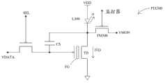
图2是根据一些实施例的像素电路或像素PIX200的示意图。像素PIX200是图1中的像素PIX的实现。在一些实施例中,用于像素PIX200的晶体管TM、TD和TS中的每一个的操作电压值VDD约为20V。使用其他操作电压值的晶体管也在多个实施例的范围内。FIG. 2 is a schematic diagram of a pixel circuit or pixel PIX 200 according to some embodiments. Pixel PIX 200 is an implementation of pixel PIX in FIG. 1 . In some embodiments, the operating voltage value VDD for each of the transistors TM, TD and TS of the pixel PIX200 is about 20V. Transistors using other operating voltage values are also within the scope of various embodiments.
在一些实施例中,像素PIX200具有红(R)、绿(G)和蓝(B)分量,由此三个不同电路用于三种相应颜色。像素PIX200中的每个OLED L都基于OLED L的亮度提供不同颜色。像素PIX200中具有三种不同颜色的三个OLED L的亮度提供用于像素PIX200的唯一颜色。为了说明,示出具有用于一种颜色的电路和相应OLED L的像素PIX200。用于其他颜色的电路类似。除RGB之外的颜色也在多个实施例的范围内。In some embodiments, pixel PIX200 has red (R), green (G) and blue (B) components, whereby three different circuits are used for the three respective colors. Each OLED L in Pixel PIX200 provides a different color based on the brightness of the OLED L. The brightness of the three OLED Ls with three different colors in pixel PIX200 provides a unique color for pixel PIX200. For illustration, a pixel PIX 200 is shown with circuitry for one color and a corresponding OLED L. Circuits are similar for other colors. Colors other than RGB are also within the scope of various embodiments.
OLED L的正端子与PMOS晶体管TD的漏极耦合,而OLED L的负端子接收参考电压VSS,其在一些实施例中接地。有效地,OLED L用作用于电流ITD从PMOS晶体管TD流向地的电流路径。换句话说,晶体管TD用作用于OLED L的电流源,同时OLED L用作用于晶体管TD的电流宿(current sink)。例如,当晶体管TD和OLED被激活时,电流ITD从操作电压VDD通过晶体管TD和OLED L流到地。The positive terminal of OLED L is coupled to the drain of PMOS transistor TD, while the negative terminal of OLED L receives a reference voltage VSS, which in some embodiments is grounded. Effectively, OLED L acts as a current path for current ITD to flow from PMOS transistor TD to ground. In other words, transistor TD acts as a current source for OLED L, while OLED L acts as a current sink for transistor TD. For example, when transistor TD and OLED are activated, current ITD flows from operating voltage VDD through transistor TD and OLED L to ground.
PMOS晶体管TD驱动OLED L。例如,晶体管TD提供从晶体管TD的源极流到漏极的驱动电流ITD并且通过OLED L以点亮OLED L。OLEDL的亮度与电流ITD的绝对值成比例。例如,电流ITD的绝对值越高,OLEDL就越亮。相反,电流ITD的绝对值越低,OLED L越不亮。PMOS transistor TD drives OLED L. For example, the transistor TD supplies the driving current ITD flowing from the source to the drain of the transistor TD and passes through the OLED L to light the OLED L. The brightness of OLEDL is proportional to the absolute value of current ITD. For example, the higher the absolute value of the current ITD, the brighter the OLEDL. On the contrary, the lower the absolute value of the current ITD is, the less bright the OLED L is.
晶体管TD具有浮栅FG以存储电荷,并且在一些实施例中,浮栅FG由金(Au)制成。用于浮栅FG的其他材料也在多个实施例的范围内。晶体管TD的阈值电压VTHTD(未标记)基于存储在浮栅FG中的电荷量可调节。在一些实施例中,为了增加阈值电压VTHTD的绝对值|VTHTD|,附加电荷被注入浮栅FG。当阈值电压VTHTD增加时,电流ITD的绝对值|ITD|减小,其减小OLED L的亮度。在一些实施例中,晶体管TD是薄膜晶体管(TFT)。此外,因为晶体管TD具有浮栅FG,所以晶体管TD被称为浮栅TFT。在一些实施例中,诸如150℃的较低温度被用于在用于显示器的玻璃和/或塑料基板上制造TFT。晶体管TD被选择为薄膜晶体管,这是因为薄膜晶体管TD能够适于玻璃和/或塑料的低温规范。然而,其他类型的晶体管也在多个实施例的范围内。示例性晶体管包括低温多晶硅(LTPS)晶体管、金属氧化物晶体管、加氢非晶硅(a-Si:H)晶体管、微晶体硅晶体管、有机晶体管等。Transistor TD has a floating gate FG to store charges, and in some embodiments, floating gate FG is made of gold (Au). Other materials for the floating gate FG are also within the scope of various embodiments. The threshold voltage VTHTD (not labeled) of transistor TD is adjustable based on the amount of charge stored in floating gate FG. In some embodiments, to increase the absolute value |VTHTD| of the threshold voltage VTHTD, additional charges are injected into the floating gate FG. When the threshold voltage VTHTD increases, the absolute value |ITD| of the current ITD decreases, which reduces the brightness of the OLED L. In some embodiments, transistor TD is a thin film transistor (TFT). Also, since the transistor TD has a floating gate FG, the transistor TD is called a floating gate TFT. In some embodiments, lower temperatures, such as 150°C, are used to fabricate TFTs on glass and/or plastic substrates for displays. Transistor TD is chosen as a thin film transistor because thin film transistor TD can be adapted to low temperature specifications of glass and/or plastic. However, other types of transistors are within the scope of various embodiments. Exemplary transistors include low temperature polysilicon (LTPS) transistors, metal oxide transistors, hydrogenated amorphous silicon (a-Si:H) transistors, microcrystalline silicon transistors, organic transistors, and the like.
为了说明,电压VGSTD(未标记)是晶体管TD的栅极和源极两端的电压。在一些实施例中,晶体管TD的浮栅FG中的电荷被控制,使得电压VGSTD基本上是恒定值或者电压VGSTD在可接受范围内改变。因为电流ITD的值取决于电压VGSTD,所以当电压VGSTD恒定时,电流ITD恒定。结果,OLED L的亮度处于稳定等级。To illustrate, voltage VGSTD (not labeled) is the voltage across the gate and source of transistor TD. In some embodiments, the charge in the floating gate FG of transistor TD is controlled such that the voltage VGSTD is substantially constant or the voltage VGSTD varies within an acceptable range. Since the value of the current ITD depends on the voltage VGSTD, when the voltage VGSTD is constant, the current ITD is constant. As a result, the brightness of OLED L is at a stable level.
信号VDATA被用于改变电压VGSTD的电压值,以改变OLED L的亮度。例如,当信号VDATA被传送至晶体管TD的栅极时,电荷被添加至浮栅FG。结果,阈值电压VTHTD的绝对值|VTHTD|增加,其导致电流ITD的绝对值|ITD|减小并且OLED L的亮度减小。The signal VDATA is used to change the voltage value of the voltage VGSTD to change the brightness of the OLED L. For example, when the signal VDATA is transferred to the gate of the transistor TD, charges are added to the floating gate FG. As a result, the absolute value |VTHTD| of the threshold voltage VTHTD increases, which causes the absolute value |ITD| of the current ITD to decrease and the luminance of the OLED L to decrease.
PMOS晶体管TS用作将信号VDATA传输至晶体管TD的开关。晶体管TS的栅极处的信号SEL被用于导通和截止晶体管TS。晶体管TS的源极接收信号VDATA,而晶体管TS的漏极与晶体管TD的栅极和电容器CS的一端耦合。在一些情况下,当电荷被注入晶体管TD时,晶体管TS的栅极处的信号SEL施加低逻辑值以导通PMOS晶体管TS。结果,晶体管TS的源极处的信号VDATA被传输至晶体管TS的漏极(其与晶体管TD的栅极耦合)。有效地,信号VDATA被传输至晶体管TD的栅极,以将电荷提供给晶体管TD的浮栅FG。相反地,当信号SEL是逻辑高时,PMOS晶体管TS被截止并且与晶体管TD的栅极截止电连接。结果,电压VGSTD保持在由电容器CS支持的相同电平。The PMOS transistor TS acts as a switch that transmits the signal VDATA to the transistor TD. The signal SEL at the gate of transistor TS is used to switch transistor TS on and off. The source of transistor TS receives the signal VDATA, while the drain of transistor TS is coupled to the gate of transistor TD and to one end of capacitor CS. In some cases, when charge is injected into transistor TD, signal SEL at the gate of transistor TS applies a low logic value to turn on PMOS transistor TS. As a result, the signal VDATA at the source of transistor TS is transferred to the drain of transistor TS (which is coupled to the gate of transistor TD). Effectively, signal VDATA is transmitted to the gate of transistor TD to provide charge to the floating gate FG of transistor TD. Conversely, when the signal SEL is logic high, the PMOS transistor TS is turned off and is electrically connected to the gate of the transistor TD. As a result, voltage VGSTD remains at the same level supported by capacitor CS.
电容器CS被用于稳定晶体管TD的栅极处的电压VGTD(未标记)。电容器CS的第一端与晶体管TD的栅极耦合,并且第二端与晶体管TD的源极耦合。结果,电压VGTD并且从而晶体管TD的电压VSGTD和电流ITD稳定,将OLED L的亮度保持在稳定等级。图2中示出的电容器CS的连接用于说明。稳定晶体管TD的栅极处的电压VGTD的其他连接也在多个实施例的范围内。例如,电容器CS的第二端被配置成接收稳定电压或地。代替电容器CS以稳定晶体管TD的栅极处的电压VGTD的其他电路也在多个实施例的范围内。在一些实施例中,晶体管TD的栅极处的寄生电容足以稳定电压VGTD。从而不使用电容器CS。Capacitor CS is used to stabilize the voltage VGTD (not labeled) at the gate of transistor TD. A first end of capacitor CS is coupled to the gate of transistor TD, and a second end is coupled to the source of transistor TD. As a result, voltage VGTD and thus voltage VSGTD and current ITD of transistor TD are stabilized, maintaining the brightness of OLED L at a stable level. The connection of capacitor CS shown in FIG. 2 is for illustration. Other connections to stabilize the voltage VGTD at the gate of transistor TD are also within the scope of various embodiments. For example, the second end of the capacitor CS is configured to receive a stable voltage or ground. Other circuits in place of capacitor CS to stabilize the voltage VGTD at the gate of transistor TD are also within the scope of various embodiments. In some embodiments, the parasitic capacitance at the gate of transistor TD is sufficient to stabilize voltage VGTD. Capacitor CS is thus not used.
PMOS晶体管TM用作开关,使得测量晶体管TD和OLED L的电特性。根据应用,晶体管TM的源极或漏极与晶体管TD的漏极耦合。例如,当电流ITDTM(未标记)从晶体管TD流过晶体管TM时,与晶体管TD的漏极耦合的晶体管TM的端子被配置为晶体管TM的源极。但是当电流ITMLED(未标记)从晶体管TM流过OLED L时,与晶体管TD的漏极耦合的晶体管TM的端子被配置为晶体管TM的漏极。为了说明,术语源极/漏极和漏极/源极被用于指示晶体管TM的端子被配置为源极或漏极。The PMOS transistor TM is used as a switch so that the electrical characteristics of the transistor TD and the OLED L are measured. Depending on the application, the source or drain of transistor TM is coupled to the drain of transistor TD. For example, when a current ITDTM (not labeled) flows from transistor TD through transistor TM, the terminal of transistor TM coupled to the drain of transistor TD is configured as the source of transistor TM. But when a current ITMLED (not labeled) flows from transistor TM through OLED L, the terminal of transistor TM coupled to the drain of transistor TD is configured as the drain of transistor TM. For purposes of illustration, the terms source/drain and drain/source are used to indicate that the terminals of transistor TM are configured as source or drain.
PMOS晶体管TM的源极/漏极耦合至PMOS晶体管TD的漏极和OLEDL的正节点,同时PMOS晶体管TM的漏极/源极被配置成接收电压VMON。当晶体管TM的栅极处的电压MONITOR是逻辑低时,晶体管TM被导通,电流ITDTM从晶体管TD流过晶体管TM,并且基于晶体管TM的漏极/源极处的电压VMON被测量。根据电流ITDTM、电流ITM、电流ITMLED和电压VMON中的一个或结合计算电流ITD。对于另一个实例,当晶体管TD截止并且晶体管TM导通时,从晶体管TM流过OLED L的电流ITMLED被测量以确定OLED L的老化或劣化效果。有效地,基于电压VMON的电压值,确定OLED L的劣化效果。The source/drain of PMOS transistor TM is coupled to the drain of PMOS transistor TD and the positive node of OLEDL, while the drain/source of PMOS transistor TM is configured to receive voltage VMON. When voltage MONITOR at the gate of transistor TM is logic low, transistor TM is turned on, current ITDTM flows from transistor TD through transistor TM, and is measured based on voltage VMON at the drain/source of transistor TM. Current ITD is calculated from one or a combination of current ITDTM, current ITM, current ITMLED and voltage VMON. For another example, when transistor TD is off and transistor TM is on, the current ITMLED flowing from transistor TM through OLED L is measured to determine the aging or degradation effects of OLED L. Effectively, based on the voltage value of voltage VMON, the degradation effect of OLED L is determined.
在一些实施例中,当显示器的任何一对两个像素PIX200的亮度差在可接受范围内时,显示器的亮度就被认为是均匀的。相反,如果任何一对两个像素的亮度差在可接受范围之外,则显示器的亮度是不均匀的。在一些实施例中,两个像素PIX200之间的亮度差反映在两个像素PIX200中的两个相应两个晶体管TD的两个电压VGSTD之间的电压差和/或两个像素PIX200的两个电流ITD之间的电流差。在一些实施例中,当两个电流ITD之间的电流差的值小于两个电流ITD的电流值的5%时,两个像素之间的亮度被认为是均匀的。在一些实施例中,基于显示器中的所有像素的电流ITD的电流值的分配确定亮度均匀性。例如,如果显示器中的所有像素的电流值的统计分布小于5%,则显示器的亮度被认为是均匀的。决定两个像素和/或显示器的亮度均匀性的其他值和/或方法也在多个实施例的范围内。In some embodiments, the brightness of the display is considered uniform when the difference in brightness between any pair of two pixels PIX200 of the display is within an acceptable range. Conversely, if the brightness difference between any pair of two pixels is outside the acceptable range, the brightness of the display is non-uniform. In some embodiments, the brightness difference between the two pixels PIX200 is reflected in the voltage difference between the two voltages VGSTD of the two corresponding two transistors TD in the two pixels PIX200 and/or the two voltages VGSTD of the two pixels PIX200 The current difference between current ITD. In some embodiments, the brightness between two pixels is considered uniform when the value of the current difference between the two currents ITD is less than 5% of the current value of the two currents ITD. In some embodiments, brightness uniformity is determined based on the distribution of current values of current ITD for all pixels in the display. For example, the brightness of a display is considered uniform if the statistical distribution of current values for all pixels in the display is less than 5%. Other values and/or methods of determining brightness uniformity between two pixels and/or a display are also within the scope of various embodiments.
为了说明,基于诸如图1中的两个像素PIX[i,j]和PIX[i,j+1]的两个相邻像素确定显示器的亮度均匀性。为了说明,图1中的两个像素PIX[i,j]和PIX[i,j+1]被实现为标为像素PIX200[i,j]和PIX200[i,j+1]的两个像素PIX200。此外,当像素PIX200[i,j]的电压VGSTD[j]和PIX200[i,j+1]的电压VGSTD[j+1]之间的差在可接受范围内时,或者当像素PIX200[i,j]的电流ITD[i,j]和像素PIX200[i,j+1]的电流ITD[i,j+1]之间的差在可接受范围内时,亮度是均匀的。在一些实施例中,晶体管TD的电流ITD的绝对值|ITD|与晶体管TD的阈值电压VTHTD的绝对值|VTHTD|成比例。有效地,在多个实施例中,通过使像素PIX200[i,j]的阈值电压值VTHTD[i,j]和像素PIX200[i,j+1]的阈值电压值VTHTD[i,j+1]之间的差在预定且可接受的范围内,实现亮度均匀性。当差接近零时,像素PIX200[i,j]的阈值电压值VTHTD[i,j]基本接近像素PIX200[i,j+1]的阈值电压值VTHTD[i,j+1]。To illustrate, the luminance uniformity of the display is determined based on two adjacent pixels such as the two pixels PIX[i,j] and PIX[i,j+1] in FIG. 1 . To illustrate, the two pixels PIX[i,j] and PIX[i,j+1] in FIG. 1 are implemented as two pixels denoted as pixels PIX200[i,j] and PIX200[i,j+1] PIX200. In addition, when the difference between the voltage VGSTD[j] of the pixel PIX200[i,j] and the voltage VGSTD[j+1] of the PIX200[i,j+1] is within an acceptable range, or when the pixel PIX200[i When the difference between the current ITD[i,j] of the pixel PIX200[i,j+1] and the current ITD[i,j+1] of the pixel PIX200[i,j+1] is within an acceptable range, the brightness is uniform. In some embodiments, the absolute value |ITD| of the current ITD of the transistor TD is proportional to the absolute value |VTHTD| of the threshold voltage VTHTD of the transistor TD. Effectively, in various embodiments, by having the threshold voltage value VTHTD[i,j] of pixel PIX200[i,j] and the threshold voltage value VTHTD[i,j+1] of pixel PIX200[i,j+1] ] within a predetermined and acceptable range to achieve brightness uniformity. As the difference approaches zero, threshold voltage value VTHTD[i,j] of pixel PIX200[i,j] is substantially close to threshold voltage value VTHTD[i,j+1] of pixel PIX200[i,j+1].
多个进一步实施例中的像素电路Pixel circuit in various further embodiments
图3是根据一些实施例的像素PIX300的示意图。像素PIX300是图1中的像素PIX的另一个实施例。FIG. 3 is a schematic diagram of a pixel PIX 300 according to some embodiments. Pixel PIX300 is another embodiment of pixel PIX in FIG. 1 .
与图2中的像素PIX200相比,OLED L300对应于图2中的OLED L,并且PMOS晶体管TM300对应于图2中的PMOS晶体管TM。OLED L300的位置不同于像素PIX200中的OLED L的位置。例如,OLED L300的正节点接收操作电压VDD,同时OLED L300的负节点耦合至晶体管TD的源极。有效地,OLED用作晶体管TD的电流源,并且晶体管TD用作OLEDL300的电流宿。例如,当OLED L300和晶体管TD被激活时,电流ITD从操作电压VDD流过OLED L300和晶体管TD到地。相反地,在像素PIX200中,晶体管TD用作OLED L的电流源,同时OLED用作晶体管TD的电流宿。Compared with the pixel PIX200 in FIG. 2 , the OLED L300 corresponds to the OLED L in FIG. 2 , and the PMOS transistor TM300 corresponds to the PMOS transistor TM in FIG. 2 . The position of OLED L300 is different from that of OLED L in Pixel PIX200. For example, the positive node of OLED L300 receives the operating voltage VDD, while the negative node of OLED L300 is coupled to the source of transistor TD. Effectively, the OLED acts as a current source for transistor TD, and transistor TD acts as a current sink for OLED L300. For example, when OLED L300 and transistor TD are activated, current ITD flows from operating voltage VDD through OLED L300 and transistor TD to ground. In contrast, in pixel PIX200, transistor TD serves as a current source for OLED L, while OLED serves as a current sink for transistor TD.
PMOS晶体管TM300的位置也不同于图2中的PMOS晶体管TM的位置。例如,PMOS晶体管TM300的源极/漏极耦合至OLED L300的负节点和晶体管TD的源极,同时PMOS晶体管TM300的漏极/源极接收电压VMON。The location of the PMOS transistor TM300 is also different from that of the PMOS transistor TM in FIG. 2 . For example, the source/drain of PMOS transistor TM300 is coupled to the negative node of OLED L300 and the source of transistor TD while the drain/source of PMOS transistor TM300 receives voltage VMON.
考虑OLED300和晶体管TM300的不同位置,像素PIX300的操作类似于像素PIX200的操作。Considering the different positions of OLED300 and transistor TM300, the operation of pixel PIX300 is similar to that of pixel PIX200.
图4是根据一些实施例的像素PIX400的示意图。像素PIX400是图1中的像素PIX的另一个实施例。FIG. 4 is a schematic diagram of a pixel PIX 400 according to some embodiments. Pixel PIX400 is another embodiment of pixel PIX in FIG. 1 .
与图2中的像素PIX200相比,NMOS晶体管TSN、TDN和TMN分别对应于图2中的PMOS晶体管TS、TD和TM。电容器CSN对应于电容器CS,同时OLED L400对应于OLED L。Compared with the pixel PIX200 in FIG. 2, the NMOS transistors TSN, TDN, and TMN correspond to the PMOS transistors TS, TD, and TM in FIG. 2, respectively. Capacitor CSN corresponds to capacitor CS, while OLED L400 corresponds to OLED L.
NMOS晶体管TSN、TDN和TMN、电容器CSN、以及OLED L400的连接也不同。例如,晶体管TSN的漏极接收信号VDATA,晶体管TSN的源极与晶体管TDN的栅极耦合。晶体管TDN的漏极接收操作电压VDD。晶体管TDN的源极与OLED L400的正端并且与晶体管TMN的漏极/源极耦合。有效地,晶体管TDN用作OLED L400的电流源,同时OLED L400用作晶体管TDN的电流宿。晶体管TMN的源极/漏极接收电压VMON。电容器CSN的第一端与晶体管TDN的栅极耦合,并且电容器CSN的第二端与晶体管TDN的源极耦合。图4所示的电容器CSN的连接用于说明。其他连接也在多个实施例的范围内。例如,电容器CSN的第二端代替地与提供稳定电压(诸如操作电压VDD或参考电压VSS等)的另一个电压源耦合。代替电容器CSN的用于稳定晶体管TDN的栅极处的电压的其他电路也在多个实施例的范围内。The connection of NMOS transistors TSN, TDN and TMN, capacitor CSN, and OLED L400 is also different. For example, the drain of transistor TSN receives the signal VDATA, and the source of transistor TSN is coupled to the gate of transistor TDN. The drain of the transistor TDN receives the operating voltage VDD. The source of transistor TDN is coupled to the positive terminal of OLED L400 and to the drain/source of transistor TMN. Effectively, transistor TDN acts as a current source for OLED L400, while OLED L400 acts as a current sink for transistor TDN. The source/drain of transistor TMN receives voltage VMON. A first terminal of capacitor CSN is coupled to the gate of transistor TDN, and a second terminal of capacitor CSN is coupled to the source of transistor TDN. The connection of capacitor CSN shown in Figure 4 is for illustration. Other connections are also within the scope of various embodiments. For example, the second terminal of the capacitor CSN is instead coupled to another voltage source providing a stable voltage such as an operating voltage VDD or a reference voltage VSS or the like. Other circuits for stabilizing the voltage at the gate of transistor TDN instead of capacitor CSN are also within the scope of various embodiments.
图5是根据一些实施例的像素PIX500的示意图。像素PIX500是图1中的像素PIX的另一个实施例。FIG. 5 is a schematic diagram of a pixel PIX500 according to some embodiments. Pixel PIX500 is another embodiment of pixel PIX in FIG. 1 .
与图4中的像素PIX400相比,OLED L500对应于图4中的OLED L400,并且NMOS晶体管TMN500对应于图4中的NMOS晶体管TMN。OLED L50的位置不同于像素PIX400中的OLED L400的位置。例如,OLED L500的正节点接收操作电压VDD,同时OLED L500的负节点与晶体管TDN的漏极耦合。有效地,OLED L500用作晶体管TDN的电流源,同时晶体管TDN用作OLED 500的电流宿。相反地,在图4中,晶体管TDN用作OLED L400的电流源,同时OLED L400用作晶体管TDN的电流宿。Compared with the pixel PIX400 in FIG. 4 , the OLED L500 corresponds to the OLED L400 in FIG. 4 , and the NMOS transistor TMN500 corresponds to the NMOS transistor TMN in FIG. 4 . The position of OLED L50 is different from the position of OLED L400 in Pixel PIX400. For example, the positive node of OLED L500 receives the operating voltage VDD, while the negative node of OLED L500 is coupled to the drain of transistor TDN. Effectively, OLED L500 acts as a current source for transistor TDN, while transistor TDN acts as a current sink for OLED 500. Conversely, in Fig. 4, transistor TDN acts as a current source for OLED L400, while OLED L400 acts as a current sink for transistor TDN.
NMOS晶体管TMN500的位置也不同于图4中的NMOS晶体管TMN的位置。例如,NMOS晶体管TMN500的漏极/源极与OLED L500的负节点并且与晶体管TD的漏极耦合,同时NMOS晶体管TMN500的源极/漏极接收电压VMON。The location of the NMOS transistor TMN500 is also different from that of the NMOS transistor TMN in FIG. 4 . For example, the drain/source of NMOS transistor TMN500 is coupled to the negative node of OLED L500 and to the drain of transistor TD while the source/drain of NMOS transistor TMN500 receives voltage VMON.
考虑从像素PIX400到像素PIX500的改变,像素PIX500的操作类似于像素PIX400的操作。Considering the change from the pixel PIX400 to the pixel PIX500, the operation of the pixel PIX500 is similar to that of the pixel PIX400.
在包括NMOS晶体管TSN、TDN、TMN和TMN500的图4和图5的实施例中,与包括PMOS晶体管的图2和图3的实施例相比,导通和截止相应晶体管的逻辑值相应地改变。例如,在晶体管的栅极处,PMOS晶体管由低逻辑值导通,并且由高逻辑值截止。相反地,在晶体管的栅极处,NMOS晶体管由高逻辑值导通,并且由低逻辑值截止。In the embodiment of FIG. 4 and FIG. 5 including NMOS transistors TSN, TDN, TMN and TMN500, compared with the embodiment of FIG. 2 and FIG. 3 including PMOS transistors, the logic values for turning on and off the corresponding transistors are changed accordingly . For example, a PMOS transistor is turned on by a low logic value and turned off by a high logic value at the gate of the transistor. Conversely, an NMOS transistor is turned on by a high logic value and turned off by a low logic value at the gate of the transistor.
基于I-V曲线关系的亮度均匀性Brightness Uniformity Based on I-V Curve Relationship
图6是根据一些实施例的图2中的两个晶体管TD的电流-电压(I-V)关系的曲线图。x轴指示像素的晶体管TD的电压VSGTD。y轴指示相同像素的晶体管TD的电流ITD。曲线610表示像素PIX200[i,j]的晶体管TD的电压VSGTD[i,j]和电流ITD[i,j]之间的关系,而曲线620表示像素PIX200[i,j+1]的晶体管TD的电压VSGTD[i,j+1]和电流ITD[i,j+1]之间的关系。曲线610和620用于基于两个电流ITD[i,j]和ITD[i,j+1]示出两个像素PIX200[i,j]和PIX200[i,j+1]之间的亮度均匀性。FIG. 6 is a graph of the current-voltage (I-V) relationship of two transistors TD in FIG. 2 according to some embodiments. The x-axis indicates the voltage VSGTD of the transistor TD of the pixel. The y-axis indicates the current ITD of the transistor TD of the same pixel.
在x轴上的特定电压VSGTD0处,存在电流ITD[i,j]和电流ITD[i,j+1]之间的电流差ΔITD。在一些实施例中,基于诸如信号VDATA的电压值的一半的信号VDATA的电压值,确定电压VSGTD0。对于另一个实例,晶体管TD的源极处的电压VDD是20V。信号VDATA的电压值是15V。从而信号VDATA的电压值的一半是7.5V。结果,电压VSGTD0是7.5V-20V或者-12.5V。用于电压VSGTD0的其他值也在多个实施例的范围内。At a certain voltage VSGTD0 on the x-axis, there is a current difference ΔITD between the current ITD[i,j] and the current ITD[i,j+1]. In some embodiments, voltage VSGTD0 is determined based on a voltage value of signal VDATA, such as half the voltage value of signal VDATA. For another example, the voltage VDD at the source of transistor TD is 20V. The voltage value of the signal VDATA is 15V. Thus half the voltage value of the signal VDATA is 7.5V. As a result, voltage VSGTD0 is 7.5V-20V or -12.5V. Other values for voltage VSGTD0 are also within the scope of various embodiments.
在一些实施例中,像素PIX200[i,j]的阈值电压VTHTD[i,j+1]的值和/或像素PIX200[i,j+1]的阈值电压VTHTD[i,j+1]的值被调节,使得电流差ΔITD在预定范围内。结果,像素PIX200[i,j]和像素PIX200[i,j+1]的两个OLED L之间的亮度差在可接受等级内。换句话说,像素PIX200[i,j]和像素PIX200[i,j+1]的亮度是均匀的。在一些实施例中,行中的像素PIX200被选择作为具有基本电流的基本像素。例如,在行中的像素中具有最小值的电流ITD的像素PIX200被选择作为基本像素PIX200。相同行中的其他像素PIX200的阈值电压ITD被调节,使得基本像素PIX200的电流ITD和相同行中的每个其他像素PIX200的电流ITD之间的电流差ITD在可接受范围内。结果,基本像素PIX200和相同行中的其他像素PIX200中的每个之间的亮度是均匀的。In some embodiments, the value of threshold voltage VTHTD[i,j+1] of pixel PIX200[i,j] and/or the value of threshold voltage VTHTD[i,j+1] of pixel PIX200[i,j+1] The value is adjusted so that the current difference ΔITD is within a predetermined range. As a result, the luminance difference between the two OLEDs L of the pixel PIX200[i,j] and the pixel PIX200[i,j+1] is within an acceptable level. In other words, the brightness of the pixel PIX200[i,j] and the pixel PIX200[i,j+1] is uniform. In some embodiments, pixels PIX200 in a row are selected as elementary pixels with elementary currents. For example, the pixel PIX200 having the smallest value of the current ITD among the pixels in the row is selected as the basic pixel PIX200. The threshold voltage ITD of other pixels PIX200 in the same row is adjusted such that the current difference ITD between the current ITD of the basic pixel PIX200 and the current ITD of each other pixel PIX200 in the same row is within an acceptable range. As a result, luminance is uniform between the basic pixel PIX200 and each of the other pixels PIX200 in the same row.
以类似方式实现另一行中的像素的亮度均匀性。在一些实施例中,一旦行的亮度均匀性被确定,行中的电流ITD的值就被用作用于下一行的基本电流值。例如,电流ITD的平均值或行的电流ITD的最小值被用作基本电流值。在一些其他实施例中,从下一行中的电流值中选择的电流值被用作基本电流值。在一些实施例中,像素阵列或显示器中的所有电流值中的一个电流值被用作基本电流值。确定像素阵列电路100中的不同像素之间的电流差ITD的不同方式也在多个实施例的范围内。换句话说,基于两个不同像素的电流ITD确定像素阵列100的亮度均匀性的不同方式也在多个实施例的范围内。The brightness uniformity of the pixels in the other row is achieved in a similar manner. In some embodiments, once the brightness uniformity of a row is determined, the value of current ITD in a row is used as the base current value for the next row. For example, the average value of the current ITD or the minimum value of the current ITD of the row is used as the basic current value. In some other embodiments, a current value selected from the current values in the next row is used as the base current value. In some embodiments, one current value out of all current values in the pixel array or display is used as the base current value. Different ways of determining the current difference ITD between different pixels in the pixel array circuit 100 are also within the scope of various embodiments. In other words, different ways of determining the brightness uniformity of the pixel array 100 based on the current ITD of two different pixels are also within the scope of various embodiments.
调节阈值电压的电荷注入Charge Injection to Adjust Threshold Voltage
在一些实施例中,通过将相应电荷注入到相同晶体管TD的浮栅FG中,调节像素PIX200的晶体管TD的阈值电压VTHTD。在一些实施例中,晶体管TD(例如,如图2所示)的漏极和源极接收0V的电压值,并且晶体管TD的栅极被施加有电脉冲。在一些实施例中,脉冲的幅度约为由晶体管TD的栅极正常接收的电压的三倍。例如,晶体管TD的栅极正常接收约-20V的电压。从而,脉冲的幅度约为-60V。脉冲的时间周期约为50ms。为了说明,时间周期被称为应力(stress)时间,并且脉冲的幅度被称为应力电压。在一些实施例中,PMOS晶体管TS的栅极被施加有-40V的电压值以导通晶体管TS。晶体管TS的源极处的信号VDATA被提供有脉冲,其然后被传输至晶体管TS的漏极或晶体管TD的栅极。In some embodiments, the threshold voltage VTHTD of transistor TD of pixel PIX200 is adjusted by injecting a corresponding charge into the floating gate FG of the same transistor TD. In some embodiments, the drain and source of transistor TD (eg, as shown in FIG. 2 ) receive a voltage value of 0V, and the gate of transistor TD is applied with an electrical pulse. In some embodiments, the amplitude of the pulse is approximately three times the voltage normally received by the gate of transistor TD. For example, the gate of transistor TD normally receives a voltage of about -20V. Thus, the amplitude of the pulse is about -60V. The time period of the pulse is about 50ms. For illustration, the period of time is referred to as the stress time, and the amplitude of the pulse is referred to as the stress voltage. In some embodiments, the gate of the PMOS transistor TS is applied with a voltage value of -40V to turn on the transistor TS. The signal VDATA at the source of transistor TS is provided with pulses, which are then transferred to the drain of transistor TS or the gate of transistor TD.
应力电压和/或应力时间基于不同标准被选择,诸如调节像素阵列电路100中的每个特定像素和所有像素的阈值电压VTHTD的时间、可损害晶体管TD的应力电压和/或应力周期。例如,当使用约为电压VDD的两倍的-40V的应力电压时,晶体管TD存在被损害的较小风险,但是将电荷注入到浮栅FG中的时间更长,从而调节阈值电压VTHTD的时间更长。约为操作电压VDD的四倍的约-80V的应力电压导致对晶体管TD的不可逆损害,从而不被使用。在一些实施例中,-40V的应力电压和50mS的应力时间被使用并且通过仿真实现。The stress voltage and/or stress time are selected based on different criteria, such as the time to adjust the threshold voltage VTHTD of each specific pixel and all pixels in the pixel array circuit 100 , the stress voltage and/or stress period that can damage the transistor TD. For example, when using a stress voltage of -40V, which is about twice the voltage VDD, there is less risk of transistor TD being damaged, but the time to inject charge into the floating gate FG is longer, and thus the time to regulate the threshold voltage VTHTD longer. A stress voltage of about -80V, which is about four times the operating voltage VDD, causes irreversible damage to the transistor TD and is therefore not used. In some embodiments, a stress voltage of -40V and a stress time of 50mS were used and achieved by simulation.
为了说明,当晶体管TD被完全导通并且在饱和模式下操作时,传导电流ITDON表示电流ITD,并且当晶体管TD经受电荷注入时,ITDINJECT表示电流ITD。在一些实施例中,当电压VDSTD是0V时,晶体管TD经受电荷注入。此外,当电压VDSTD是0V时,电流ITDON减小六阶(order)。换句话说,电流ITDON减小六阶的幅度到电流ITDINJECT。数学上表达为,当电压VDSTD是0V时,ITDINJECT=ITDON*10-6或更少。在一些实施例中,电流ITDINJECT小于1nA。To illustrate, conduction current ITDON represents current ITD when transistor TD is fully turned on and is operating in saturation mode, and ITDINJECT represents current ITD when transistor TD is subject to charge injection. In some embodiments, transistor TD is subject to charge injection when voltage VDSTD is 0V. In addition, when the voltage VDSTD is 0V, the current ITDON decreases by six orders. In other words, current ITDON is reduced in magnitude by six steps to current ITDINJECT. Expressed mathematically, when the voltage VDSTD is 0V, ITDINJECT=ITDON*10−6 or less. In some embodiments, current ITDINJECT is less than 1 nA.
在一些实施例中,晶体管TD的阈值电压VTHTD与应力时间和应力电压的绝对值成比例。例如,当应力时间增加和/或应力电压的绝对值增加时,阈值电压VTHTD的绝对值|VTHTD|增加。In some embodiments, the threshold voltage VTHTD of transistor TD is proportional to the stress time and the absolute value of the stress voltage. For example, the absolute value |VTHTD| of the threshold voltage VTHTD increases when the stress time increases and/or the absolute value of the stress voltage increases.
为了说明,数学上表示为,ΔVTH是阈值电压VTHTD的电压变化,|VSTRESS|是应力电压的绝对值,TSTRESS是应力时间,α是VSTRESS的阶数,并且β是log函数的阶数。To illustrate, expressed mathematically, ΔVTH is the voltage change in threshold voltage VTHTD, |VSTRESS| is the absolute value of the stress voltage, TSTRESS is the stress time, α is the order of VSTRESS, and β is the order of the log function.
VTH=|VSTRESS|αlog β(TSTRESS)VTH=|VSTRESS|α log β(TSTRESS)
在一些实施例中,|VTH|还受特定应力脉冲被施加给晶体管TD的栅极的次数影响。例如,在选择应力脉冲之后,诸如以-60V和50mS,每当应力脉冲被再次施加给晶体管TD的栅极时绝对值|VTH|保持增加。在诸如约5-10次的次数之后,|VTH|不再改变而是保持在恒定值。换句话说,继续将应力脉冲施加至晶体管TD的栅极不导致晶体管TD的阈值电压VTHTD的任何附加改变。在一些实施例中,继续导致阈值电压VTHTD改变的应力脉冲被施加至晶体管TD的栅极的次数通过仿真实现。In some embodiments, |VTH| is also affected by the number of times a particular stress pulse is applied to the gate of transistor TD. For example, after a selected stress pulse, such as at -60V and 50mS, the absolute value |VTH| keeps increasing each time the stress pulse is applied again to the gate of transistor TD. After a number of times such as about 5-10 times, |VTH| does not change but remains at a constant value. In other words, continuing to apply the stress pulse to the gate of transistor TD does not result in any additional change in the threshold voltage VTHTD of transistor TD. In some embodiments, the number of times a stress pulse is applied to the gate of transistor TD that continues to cause a change in threshold voltage VTHTD is achieved by simulation.
测量电流ITDMeasurement current ITD
在一些实施例中,使用超速传动技术测量电流ITD,其中,所测量的电流受晶体管TD而不是晶体管TM控制,这是因为来自操作电压VDD的大多数压降都通过晶体管TD而不是晶体管TM。例如,当测量电流ITD时,晶体管TS的栅极被施加有-40V的电压值,以导通晶体管TS。信号VDATA的电压值被配置成接近晶体管TD的阈值电压VTHTD,以确保所测量的电流ITD不受晶体管TM的阈值电压VTHTM的改变影响。晶体管TD的源极处的电压VDD被设置为0V,并且OLED L的一端处的电压VSS被设置为0V。不同电压值在多个实施例的范围内。例如,晶体管TD的源极和OLED的一端被设置为相同电压值。结果。OLED L被截止。晶体管TM的栅极还被施加有-40V的电压值以导通晶体管TM。电压VMON被设置为约-13V,使得晶体管TD和TM被导通,而OLED L被截止。电流ITDTM被测量,在一些实施例中,其是电流ITD,这是因为大多数压降都通过晶体管TD。In some embodiments, current ITD is measured using an overdrive technique, where the measured current is controlled by transistor TD rather than transistor TM because most of the voltage drop from operating voltage VDD passes through transistor TD rather than transistor TM. For example, when measuring the current ITD, the gate of the transistor TS is applied with a voltage value of -40V to turn on the transistor TS. The voltage value of signal VDATA is configured to be close to the threshold voltage VTHTD of transistor TD to ensure that the measured current ITD is not affected by changes in the threshold voltage VTHTM of transistor TM. The voltage VDD at the source of the transistor TD is set to 0V, and the voltage VSS at one terminal of the OLED L is set to 0V. Different voltage values are within the scope of various embodiments. For example, the source of the transistor TD and one terminal of the OLED are set to the same voltage value. result. OLED L is turned off. The gate of transistor TM is also applied with a voltage value of -40V to turn on transistor TM. Voltage VMON is set to about -13V, so that transistors TD and TM are turned on and OLED L is turned off. Current ITDTM is measured, which in some embodiments is current ITD because most of the voltage drop is through transistor TD.
在一些实施例中,电流ITD的精度受到晶体管TS的栅极电压影响。例如,当信号SEL被设置为-20V时,电流IDT的误差比信号SEL在-40V时更高。执行仿真以确定导致测量电流ITD的可接受误差的信号SEL的电压值。In some embodiments, the accuracy of current ITD is affected by the gate voltage of transistor TS. For example, when the signal SEL is set to -20V, the error of the current IDT is higher than when the signal SEL is at -40V. Simulations are performed to determine the voltage value of signal SEL that results in an acceptable error in measuring current ITD.
OLED劣化OLED degradation
在一些实施例中,OLED L在使用一段时间之后劣化。时间周期和劣化等级根据特定OLED和技术而改变。由于劣化效果,OLED L采用更大量电流以具有与劣化前相同的亮度等级。在一些实施例中,考虑OLED L的劣化以确定阵列像素电路100中的像素的亮度的均匀性。例如,确定使OLED L达到劣化之前的亮度等级的附加电流量。电流ITD增加相同量以补偿劣化效果。为了说明,附加电流被称为劣化补偿电流。In some embodiments, the OLED L degrades after a period of use. Time periods and degradation levels vary according to the specific OLED and technology. Due to the degradation effect, OLED L uses a larger amount of current to have the same brightness level as before degradation. In some embodiments, the degradation of OLED L is considered to determine the uniformity of brightness of the pixels in array pixel circuit 100. For example, the amount of additional current to bring the OLED L up to the brightness level before degradation is determined. Current ITD is increased by the same amount to compensate for the degradation effect. For illustration, the additional current is referred to as degradation compensation current.
在一些实施例中,为了测量劣化补偿电流,晶体管TD被截止。例如,晶体管TS的栅极(例如,如图2所示)被施加有约-40V的电压值,以导通晶体管TS。信号VDATA被设置为10V,其被传送至晶体管TD的栅极。栅极处接收约10V的电压值的PMOS晶体管TD由此被截止。PMOS晶体管TM的栅极施加有约-40V的电压值以导通晶体管TM。晶体管TM的漏极和源极两端的电压被设置为更接近OLED L的阈值电压以导通OLED L。电流ITMLED的预定值被提供给晶体管TM的源极/漏极并且流过晶体管TM和OLED L。电流ITMLED的值基于OLED特性和技术改变。然后,测量电压MON。在一些实施例中,提供表格,以将所测量的电压VMON的值映射至表格中的电流的相应值。用于表格中的电压和电流的值被预先确定用于特定OLED技术,并由此基于不同技术而不同。如果所测量的电压VMON和预定电流ITMLED的值与表格中的相应电压和电流匹配,则OLED的劣化未发生。但是如果电压VMON和预定电流ITMLED的值与表格中的电压和电流不匹配,则劣化发生。例如,对应于所测量电压VMON的表格中的电压对应于表格中的较低电流值,OLED L的劣化发生。电流ITMLED的预定值与表格中的电流的差是劣化补偿电流。在一些实施例中,OLED L的一端处的电压VSS约为-20V,电流ITMLED约为500uA,并且电压VMON约为-13V。In some embodiments, to measure the degradation compensation current, transistor TD is turned off. For example, the gate of transistor TS (eg, as shown in FIG. 2 ) is applied with a voltage value of about -40V to turn on transistor TS. Signal VDATA is set to 10V, which is delivered to the gate of transistor TD. The PMOS transistor TD, which receives a voltage value of approximately 10V at its gate, is thus turned off. The gate of the PMOS transistor TM is applied with a voltage value of about -40V to turn on the transistor TM. The voltage across the drain and source of transistor TM is set closer to the threshold voltage of OLED L to turn on OLED L. A predetermined value of current ITMLED is supplied to the source/drain of transistor TM and flows through transistor TM and OLED L. The value of current ITMLED varies based on OLED characteristics and technology. Then, the voltage MON is measured. In some embodiments, a table is provided to map measured values of voltage VMON to corresponding values of current in the table. The values for the voltages and currents in the tables are predetermined for a particular OLED technology and thus vary from technology to technology. If the measured values of voltage VMON and predetermined current ITMLED match the corresponding voltages and currents in the table, no degradation of the OLED has occurred. But if the values of voltage VMON and predetermined current ITMLED do not match the voltage and current in the table, degradation occurs. For example, a voltage in the table corresponding to the measured voltage VMON corresponds to a lower current value in the table, and degradation of the OLED L occurs. The difference between the predetermined value of the current ITMLED and the current in the table is the degradation compensation current. In some embodiments, the voltage VSS at one terminal of OLED L is about -20V, the current ITMLED is about 500uA, and the voltage VMON is about -13V.
示例性方法exemplary method
图7是根据一些实施例的增加像素PIX[i,j]和像素PIX[i,j+1]之间的亮度均匀性的方法700的流程图。FIG. 7 is a flowchart of a
在操作705中,像素PIX被选择作为将电流ITD作为基本电流的基本像素。在一些实施例中,具有一行像素中的电流ITD的最小值的像素PIX被选择作为基本像素。为了说明,与相同第i行中的其他像素的电流相比,像素PIX[i,j]的电流ITD[i,j]具有最小电流值。像素PIX[i,j]从而被选择作为基本像素。In operation 705, the pixel PIX is selected as a basic pixel having the current ITD as a basic current. In some embodiments, the pixel PIX having the smallest value of current ITD in a row of pixels is selected as the base pixel. To illustrate, current ITD[i,j] of pixel PIX[i,j] has a minimum current value compared to the currents of other pixels in the same i-th row. Pixel PIX[i,j] is thus selected as a basic pixel.
在操作710中,确定电流ITD[i,j]和电流ITD[i,j+1]之间的电流差ΔITD。例如,基于图6中的曲线610和620确定电流差ΔITD。In
在操作715中,调节电流差ΔITD以包括像素PIX[i,j]和像素PIX[i,j+1]中的OLED L的劣化效果。例如,用于像素PIX[i,j]和像素PIX[i,j+1]中的每个OLED L的劣化补偿电流被确定,并且被添加至电流差ΔITD,以得到电流差ΔITD1。In
在操作720中,确定电流差ΔITD1是否在预定可接受范围内。如果电流差ΔITD1在预定可接受范围内,则方法在操作750结束。因为像素PIX[i,j]和像素PIX[i,j+1]的晶体管TD的电流差ΔITD1在预定范围内,像素PIX[i,j]和像素PIX[i,j+1]之间的亮度被认为是均匀的。In
然而,如果电流差ΔITD1不在预定可接受范围内,则在操作725中,基于电流差ΔITD1确定调节像素PIX[i,j+1]的晶体管TD的阈值电压VTHTD的电压量。在一些实施例中,阈值电压VTHTD和电流ITD与以下等式相关:However, if the current difference ΔITD1 is not within the predetermined acceptable range, a voltage amount to adjust the threshold voltage VTHTD of the transistor TD of the pixel PIX[i,j+1] is determined based on the current difference ΔITD1 in
ITD=1/2*(W/L)*μCOX*(VGSTD-VTHTD)2ITD=1/2*(W/L)*μCOX *(VGSTD-VTHTD)2
其中,W是晶体管TD的宽度,L是晶体管TD的长度,μ是载流子迁移率,COX是晶体管TD的栅极电容。Where, W is the width of the transistor TD, L is the length of the transistor TD, μ is the carrier mobility, and COX is the gate capacitance of the transistor TD.
在操作730中,确定应力脉冲以提供相应电荷,从而调节像素PIX[i,j+1]的晶体管TD的阈值电压VTHTD。确定应力脉冲包括确定应力电压和应力时间。一旦确定了应力脉冲,应力脉冲就被施加至像素PIX[i,j+1]的晶体管TD的栅极。In
在操作735中,重新计算电流差ΔITD1。In operation 735, the current difference ΔITD1 is recalculated.
在操作740中,确定电流差ΔITD1是否在预定可接受范围内。如果不在,则应力脉冲被确定并在操作730中被再次施加。然而,如果电流差ΔITD1在预定可接受范围内,则方法在操作750结束。在一些实施例中,当在操作740中电流差ΔITD1不在预定可接受范围内时,方法返回到操作725并且继续。例如,在操作725中,基于在操作735中重新计算的电流差ΔITD1确定调节像素PIX[i,j+1]的晶体管TD的阈值电压VTHTD的电压量。In
在一些实施例中,行中的每对两个像素的亮度均匀性使用方法700确定。然后,针对整个显示器确定行的每对像素之间的亮度均匀性。在一些其他实施例中,确定整个显示器中的每对两个像素的亮度均匀性。结果,实现显示器中的像素的亮度均匀性。本公开的实施例不限于特定方法。In some embodiments, brightness uniformity for each pair of two pixels in a row is determined using
被用作基本像素的像素PIX[i,j]用于说明。类似地,像素PIX[i,j]的电流ITD[i,j]和像素PIX[i,j+1]的电流[i,j+1]之间的电流差ΔITD和/或电流差ΔITD1也用于说明。另一个像素被用作基本像素,并且基本像素和另一个像素之间的电流差也在多个实施例的范围内。A pixel PIX[i,j] used as a basic pixel is used for illustration. Similarly, the current difference ΔITD and/or the current difference ΔITD1 between the current ITD[i,j] of the pixel PIX[i,j] and the current [i,j+1] of the pixel PIX[i,j+1] is also for illustration. Another pixel is used as the base pixel, and the current difference between the base pixel and the other pixel is also within the scope of various embodiments.
以上说明中使用的像素PIX和PIX200也用于说明。发明思想可应用至其他像素,诸如像素PIX300、像素PIX400和像素PIX500。The pixels PIX and PIX200 used in the above description are also used for illustration. The inventive concept may be applied to other pixels, such as the pixel PIX300, the pixel PIX400, and the pixel PIX500.
已经描述了多个实施例。将理解,可以在不脱离本公开的精神和范围的情况下做出多种修改。例如,被示出为特定掺杂类型(例如,N型或P型金属氧化物半导体(NMOS或PMOS))的多种晶体管用于说明目的。本公开的实施例不限于特定类型。选择用于特定晶体管的不同掺杂类型在多种实施例的范围内。在以上说明中使用的多种信号的低或高逻辑值也用于说明。当信号被激活和/或去激活时,多种实施例不限于特定电平。选择不同电平在多个实施例的范围内。在多种实施例中,晶体管用作开关。代替晶体管使用的开关电流也在多个实施例的范围内。A number of embodiments have been described. It will be understood that various modifications may be made without departing from the spirit and scope of the present disclosure. For example, various transistors are shown as being of a particular doping type (eg, N-type or P-type metal-oxide-semiconductor (NMOS or PMOS)) for illustration purposes. Embodiments of the present disclosure are not limited to a specific type. Selecting different doping types for a particular transistor is within the scope of various embodiments. Low or high logic values for various signals used in the above description are also used for illustration. Various embodiments are not limited to specific levels when signals are activated and/or deactivated. Selecting different levels is within the scope of various embodiments. In various embodiments, transistors are used as switches. Switching currents used instead of transistors is also within the scope of various embodiments.
在一些实施例中,实现增加显示器中的第一像素和第二像素之间的亮度均匀性的方法。确定第一像素的电流值。确定第二像素的电流值。调节第一像素的电流值或第二像素的电流值中的至少一个,直到第一像素的电流值和第二像素的电流值之间的电流差的值可接受为止。第一像素的电流值对应于第一像素的亮度等级。第二像素的电流值对应于第二像素的亮度等级。调节第一像素的电流值包括调节第一像素的晶体管的阈值电压值。调节第二像素的电流值包括调节第二像素的晶体管的阈值电压值。In some embodiments, a method of increasing brightness uniformity between a first pixel and a second pixel in a display is implemented. A current value for the first pixel is determined. A current value for the second pixel is determined. At least one of the current value of the first pixel or the current value of the second pixel is adjusted until the value of the current difference between the current value of the first pixel and the current value of the second pixel is acceptable. The current value of the first pixel corresponds to the brightness level of the first pixel. The current value of the second pixel corresponds to the brightness level of the second pixel. Adjusting the current value of the first pixel includes adjusting a threshold voltage value of a transistor of the first pixel. Adjusting the current value of the second pixel includes adjusting a threshold voltage value of a transistor of the second pixel.
在一些实施例中,显示器的像素电路包括第一晶体管、第一开关、第二开关和发光二极管。第一晶体管具有第一端子、第二端子和第三端子。第一晶体管的阈值电压可调节。第一晶体管的第一端子与第一开关耦合。像素电路被配置成满足以下条件中的至少一个:1)LED的第一端(PMOS/负NMOS)与第二开关并且与第一晶体管的第三端子耦合;或者2)LED的第二端(PMOS/正NMOS)与第二开关并且与第一晶体管的第二端子耦合。In some embodiments, a pixel circuit of a display includes a first transistor, a first switch, a second switch, and a light emitting diode. The first transistor has a first terminal, a second terminal and a third terminal. The threshold voltage of the first transistor is adjustable. A first terminal of the first transistor is coupled to the first switch. The pixel circuit is configured to satisfy at least one of the following conditions: 1) the first terminal (PMOS/negative NMOS) of the LED is coupled to the second switch and to the third terminal of the first transistor; or 2) the second terminal of the LED ( PMOS/positive NMOS) is coupled to the second switch and to the second terminal of the first transistor.
在一些实施例中,显示器的像素电路包括第一晶体管、第一开关、第二开关和发光二极管。第一晶体管被配置成提供用于LED的电流。LED的亮度等级基于由第一晶体管提供的电流的电流值。第一开关被配置成将信号提供给第一晶体管的浮栅。由第一开关提供的信号用于在调节第一晶体管的浮栅中的电荷时使用。第二开关被配置为第一电流路径和/或第二电流路径。第一电流路径被配置成由第一晶体管提供并且流过第二开关的电流使用。第二电流路径被配置成由流过第二开关和LED的电流使用。In some embodiments, a pixel circuit of a display includes a first transistor, a first switch, a second switch, and a light emitting diode. The first transistor is configured to provide current for the LED. The brightness level of the LED is based on the current value of the current provided by the first transistor. The first switch is configured to provide a signal to the floating gate of the first transistor. The signal provided by the first switch is used in regulating the charge in the floating gate of the first transistor. The second switch is configured as the first current path and/or the second current path. The first current path is configured to be used by the current provided by the first transistor and flowing through the second switch. The second current path is configured to be used by current flowing through the second switch and the LED.
示出电容器的多个图用于说明。等效电路在多种实施例的范围内。例如,诸如电容器、电容器件、电路等的结合的电容器件、电路或网络可以代替电容器被使用。Several figures showing capacitors are used for illustration. Equivalent circuits are within the scope of various embodiments. For example, a combined capacitive device, circuit or network such as a capacitor, capacitive device, circuit, etc. may be used instead of a capacitor.
以上说明包括典型步骤,但是步骤不必须按照所示的顺序执行。根据所公开的实施例的精神和范围,当合适时,步骤可以被添加、代替、改变顺序和/或删除。The above description includes typical steps, but the steps do not have to be performed in the order shown. Steps may be added, substituted, changed order, and/or deleted where appropriate, in accordance with the spirit and scope of the disclosed embodiments.
Claims (15)
Translated fromChinesePriority Applications (1)
| Application Number | Priority Date | Filing Date | Title |
|---|---|---|---|
| CN201510616544.5ACN105161056B (en) | 2012-06-29 | 2013-04-03 | Pixel for display |
Applications Claiming Priority (2)
| Application Number | Priority Date | Filing Date | Title |
|---|---|---|---|
| US13/539,181 | 2012-06-29 | ||
| US13/539,181US20140002332A1 (en) | 2012-06-29 | 2012-06-29 | Pixels for display |
Related Child Applications (1)
| Application Number | Title | Priority Date | Filing Date |
|---|---|---|---|
| CN201510616544.5ADivisionCN105161056B (en) | 2012-06-29 | 2013-04-03 | Pixel for display |
Publications (2)
| Publication Number | Publication Date |
|---|---|
| CN103514834Atrue CN103514834A (en) | 2014-01-15 |
| CN103514834B CN103514834B (en) | 2016-06-08 |
Family
ID=49777578
Family Applications (2)
| Application Number | Title | Priority Date | Filing Date |
|---|---|---|---|
| CN201510616544.5AActiveCN105161056B (en) | 2012-06-29 | 2013-04-03 | Pixel for display |
| CN201310116389.1AActiveCN103514834B (en) | 2012-06-29 | 2013-04-03 | Pixel for display |
Family Applications Before (1)
| Application Number | Title | Priority Date | Filing Date |
|---|---|---|---|
| CN201510616544.5AActiveCN105161056B (en) | 2012-06-29 | 2013-04-03 | Pixel for display |
Country Status (2)
| Country | Link |
|---|---|
| US (2) | US20140002332A1 (en) |
| CN (2) | CN105161056B (en) |
Cited By (5)
| Publication number | Priority date | Publication date | Assignee | Title |
|---|---|---|---|---|
| CN108269530A (en)* | 2016-09-27 | 2018-07-10 | 广东欧珀移动通信有限公司 | Brightness adjusting method of AMO L ED display screen and related product |
| WO2019218713A1 (en)* | 2018-05-14 | 2019-11-21 | 京东方科技集团股份有限公司 | Display panel and display device |
| CN111415619A (en)* | 2020-03-10 | 2020-07-14 | 华南理工大学 | A method and system for eliminating residual image and improving service life of OLED screen |
| CN114822381A (en)* | 2022-04-29 | 2022-07-29 | 湖北长江新型显示产业创新中心有限公司 | Pixel circuit, driving method thereof, display panel and display device |
| CN115568288A (en)* | 2021-04-30 | 2023-01-03 | 戴洛格半导体(英国)有限公司 | current driver |
Families Citing this family (9)
| Publication number | Priority date | Publication date | Assignee | Title |
|---|---|---|---|---|
| CN103681772B (en)* | 2013-12-27 | 2018-09-11 | 京东方科技集团股份有限公司 | A kind of array substrate and display device |
| US10410584B2 (en)* | 2017-05-08 | 2019-09-10 | Shenzhen China Star Optoelectronics Semiconductor Display Technology Co., Ltd. | Aging compensation system and method for OLED device |
| CN107068066A (en)* | 2017-06-22 | 2017-08-18 | 京东方科技集团股份有限公司 | Pixel compensation circuit and display device, driving method |
| US10234630B2 (en)* | 2017-07-12 | 2019-03-19 | Applied Materials, Inc. | Method for creating a high refractive index wave guide |
| US20200202783A1 (en)* | 2018-12-21 | 2020-06-25 | Int Tech Co., Ltd. | Pixel compensation circuit |
| CN112992043B (en)* | 2019-11-29 | 2022-04-12 | 深圳市大族元亨光电股份有限公司 | Display screen brightness adjusting method and display screen brightness adjusting system |
| CN112037730B (en)* | 2020-10-12 | 2025-01-10 | 北京集创北方科技股份有限公司 | Drive and electronic equipment |
| KR20240139646A (en)* | 2023-03-14 | 2024-09-24 | 삼성디스플레이 주식회사 | Pixel and method for aging the same |
| KR20240153484A (en)* | 2023-04-14 | 2024-10-23 | 삼성디스플레이 주식회사 | Light emitting display device and manufacturing method thereof |
Citations (3)
| Publication number | Priority date | Publication date | Assignee | Title |
|---|---|---|---|---|
| CN101329837A (en)* | 2007-06-22 | 2008-12-24 | 三星Sdi株式会社 | Pixel, organic light emitting display and related methods |
| US20090225014A1 (en)* | 2008-03-06 | 2009-09-10 | Seiko Epson Corporation | Control of semiconductor light emitting element |
| CN101903936A (en)* | 2007-11-02 | 2010-12-01 | 剑桥显示技术有限公司 | Pixel driver circuits |
Family Cites Families (7)
| Publication number | Priority date | Publication date | Assignee | Title |
|---|---|---|---|---|
| US7038392B2 (en)* | 2003-09-26 | 2006-05-02 | International Business Machines Corporation | Active-matrix light emitting display and method for obtaining threshold voltage compensation for same |
| TWI267060B (en)* | 2005-05-11 | 2006-11-21 | Benq Corp | Display apparatuses, methods and machine-readable storage medium for adjusting display parameter based on display content |
| TWI330726B (en)* | 2005-09-05 | 2010-09-21 | Au Optronics Corp | Display apparatus, thin-film-transistor discharge method and electrical driving method therefor |
| EP2277163B1 (en)* | 2008-04-18 | 2018-11-21 | Ignis Innovation Inc. | System and driving method for light emitting device display |
| JP5560206B2 (en)* | 2010-04-05 | 2014-07-23 | パナソニック株式会社 | Organic EL display device and control method thereof |
| TWI407406B (en)* | 2010-12-30 | 2013-09-01 | Au Optronics Corp | Pixel driving circuit of an organic light emitting diode |
| KR102091485B1 (en)* | 2013-12-30 | 2020-03-20 | 엘지디스플레이 주식회사 | Organic light emitting display device and method for driving thereof |
- 2012
- 2012-06-29USUS13/539,181patent/US20140002332A1/ennot_activeAbandoned
- 2013
- 2013-04-03CNCN201510616544.5Apatent/CN105161056B/enactiveActive
- 2013-04-03CNCN201310116389.1Apatent/CN103514834B/enactiveActive
- 2015
- 2015-08-14USUS14/827,115patent/US10546528B2/enactiveActive
Patent Citations (3)
| Publication number | Priority date | Publication date | Assignee | Title |
|---|---|---|---|---|
| CN101329837A (en)* | 2007-06-22 | 2008-12-24 | 三星Sdi株式会社 | Pixel, organic light emitting display and related methods |
| CN101903936A (en)* | 2007-11-02 | 2010-12-01 | 剑桥显示技术有限公司 | Pixel driver circuits |
| US20090225014A1 (en)* | 2008-03-06 | 2009-09-10 | Seiko Epson Corporation | Control of semiconductor light emitting element |
Non-Patent Citations (1)
| Title |
|---|
| TSUNG-CHING HUANG,ET AL: "A Floating-Gate OTFT-Driven AMOLED Pxiel Circuit for Variation and Degradation Compensation in Large-Sized Flexible Displays", <SID SYMPOSIUM DIGEST OF TECHNICAL PAPERS>, vol. 42, no. 1, 30 June 2011 (2011-06-30), pages 149 - 152* |
Cited By (10)
| Publication number | Priority date | Publication date | Assignee | Title |
|---|---|---|---|---|
| CN108269530A (en)* | 2016-09-27 | 2018-07-10 | 广东欧珀移动通信有限公司 | Brightness adjusting method of AMO L ED display screen and related product |
| WO2019218713A1 (en)* | 2018-05-14 | 2019-11-21 | 京东方科技集团股份有限公司 | Display panel and display device |
| JP2021521471A (en)* | 2018-05-14 | 2021-08-26 | 京東方科技集團股▲ふん▼有限公司Boe Technology Group Co.,Ltd. | Display panel and display device |
| US11380257B2 (en) | 2018-05-14 | 2022-07-05 | Beijing Boe Technology Development Co., Ltd. | Display panel and display device |
| JP7402053B2 (en) | 2018-05-14 | 2023-12-20 | 京東方科技集團股▲ふん▼有限公司 | Display panel and display device |
| CN111415619A (en)* | 2020-03-10 | 2020-07-14 | 华南理工大学 | A method and system for eliminating residual image and improving service life of OLED screen |
| CN115568288A (en)* | 2021-04-30 | 2023-01-03 | 戴洛格半导体(英国)有限公司 | current driver |
| CN115568288B (en)* | 2021-04-30 | 2023-10-31 | 瑞萨设计(英国)有限公司 | Current driver |
| CN114822381A (en)* | 2022-04-29 | 2022-07-29 | 湖北长江新型显示产业创新中心有限公司 | Pixel circuit, driving method thereof, display panel and display device |
| CN114822381B (en)* | 2022-04-29 | 2023-08-04 | 湖北长江新型显示产业创新中心有限公司 | Pixel circuit, driving method thereof, display panel and display device |
Also Published As
| Publication number | Publication date |
|---|---|
| US20140002332A1 (en) | 2014-01-02 |
| US20150356917A1 (en) | 2015-12-10 |
| CN103514834B (en) | 2016-06-08 |
| US10546528B2 (en) | 2020-01-28 |
| CN105161056B (en) | 2018-02-16 |
| CN105161056A (en) | 2015-12-16 |
Similar Documents
| Publication | Publication Date | Title |
|---|---|---|
| CN103514834B (en) | Pixel for display | |
| KR101443224B1 (en) | Pixel structure of organic light emitting diode and driving method thereof | |
| US10242625B2 (en) | Pixel driving circuit, pixel driving method and display apparatus | |
| US9269304B2 (en) | Pixel circuit for organic light emitting display and driving method thereof, organic light emitting display | |
| CN106165007B (en) | Display device and driving method thereof | |
| CN102057418B (en) | System and driving method for light emitting device display | |
| US11004383B2 (en) | Light emitting display apparatus including a plurality of pixels and method for driving thereof | |
| KR101282996B1 (en) | Organic electro-luminescent display device and driving method thereof | |
| CN110036435A (en) | Pixel circuit, active-matrix organic LED display panel, display equipment and the method for compensating drive transistor threshold voltage | |
| EP2525348A2 (en) | Pixel unit circuit and oled display apparatus | |
| US20230360570A1 (en) | Pixel circuit, display, and method | |
| WO2016070570A1 (en) | Pixel circuit, display substrate and display panel | |
| US20130175941A1 (en) | Voltage-driven pixel circuit, driving method thereof and display panel | |
| US20090167644A1 (en) | Resetting drive transistors in electronic displays | |
| KR102125785B1 (en) | Organic Light Emitting Diode Display Device | |
| CA2490858A1 (en) | Driving method for compensated voltage-programming of amoled displays | |
| KR20100045578A (en) | Organic electroluminescent display device | |
| US20150243218A1 (en) | Oled display | |
| CN111048044A (en) | Voltage programming type AMOLED pixel driving circuit and driving method thereof | |
| US9501976B2 (en) | Pixel circuit for organic light emitting display and driving method thereof, organic light emitting display | |
| US20230377494A1 (en) | Display, pixel circuit, and method | |
| KR101986657B1 (en) | Organic light emitting diode display device and method of driving the same | |
| CN105390094B (en) | A system for driving a display | |
| Huo et al. | A new pixel circuit for active matrix miniµ light emitting diodes | |
| US20240404466A1 (en) | Pixel and display device including the same |
Legal Events
| Date | Code | Title | Description |
|---|---|---|---|
| C06 | Publication | ||
| PB01 | Publication | ||
| C10 | Entry into substantive examination | ||
| SE01 | Entry into force of request for substantive examination | ||
| C14 | Grant of patent or utility model | ||
| GR01 | Patent grant |